ICGOO在线商城 > 隔离器 > 光隔离器 - 晶体管,光电输出 > PC354N1TJ00F
 Datasheet下载
- 型号: PC354N1TJ00F
- 制造商: Sharp Microelectronics
- 库位|库存: xxxx|xxxx
- 要求:
| 数量阶梯 | 香港交货 | 国内含税 |
| +xxxx | $xxxx | ¥xxxx |
查看当月历史价格
查看今年历史价格
PC354N1TJ00F产品简介:
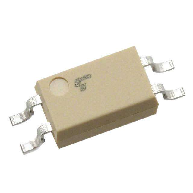
ICGOO电子元器件商城为您提供PC354N1TJ00F由Sharp Microelectronics设计生产,在icgoo商城现货销售,并且可以通过原厂、代理商等渠道进行代购。 PC354N1TJ00F价格参考。Sharp MicroelectronicsPC354N1TJ00F封装/规格:光隔离器 - 晶体管,光电输出, 光隔离器 晶体管 输出 3750Vrms 1 通道 4-Mini-Flat。您可以下载PC354N1TJ00F参考资料、Datasheet数据手册功能说明书,资料中有PC354N1TJ00F 详细功能的应用电路图电压和使用方法及教程。
Sharp Microelectronics(夏普微电子)型号为PC354N1TJ00F的器件属于光隔离器(光电耦合器)类别,具体为晶体管输出型光电耦合器。该器件主要用于实现电气隔离,同时传递电信号,常见应用场景包括:

1. 工业自动化控制:用于PLC(可编程逻辑控制器)、继电器驱动电路、传感器信号隔离等场合,防止高压干扰影响控制系统。

2. 电源管理设备:在开关电源、DC-DC转换器中用于反馈回路的信号隔离,提高系统安全性与稳定性。

3. 电机驱动电路:用于隔离控制侧与电机侧的高压电路,保护主控芯片不受损坏。

4. 通信设备:在RS-485、CAN等工业通信接口中实现信号隔离,增强抗干扰能力。

5. 家电控制板:如变频空调、洗衣机等家电中,用于隔离高低压电路,提升安全性和可靠性。

该器件具备良好的绝缘性能和抗干扰能力,适用于对电气安全要求较高的低压电子系统中。
| 参数 | 数值 |
| 产品目录 | |
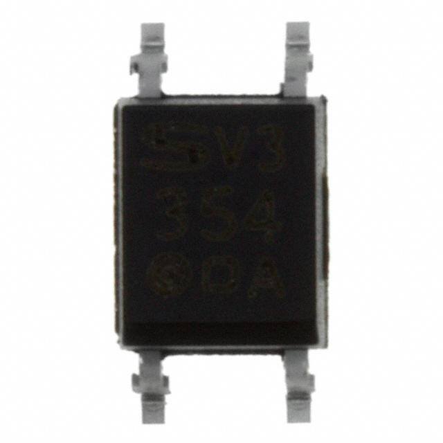
| 描述 | OPTOISOLATOR 3.75KV TRANS 4-SMD晶体管输出光电耦合器 50-150% CTR rank of PC354NTJ000F |
| 产品分类 | |
| 品牌 | Sharp Microelectronics |
| 产品手册 | |
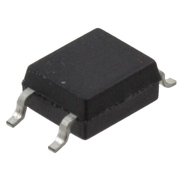
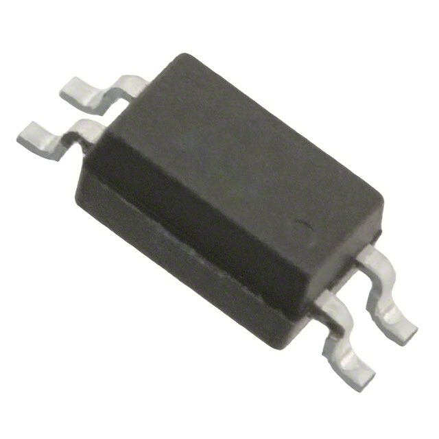
| 产品图片 |
|
| rohs | 符合RoHS无铅 / 符合限制有害物质指令(RoHS)规范要求 |
| 产品系列 | 光耦合器/光电耦合器,晶体管输出光电耦合器,Sharp Microelectronics PC354N1TJ00F- |
| 数据手册 | http://www.sharpsma.com/webfm_send/1109 |
| 产品型号 | PC354N1TJ00F |
| PCN设计/规格 | http://www.sharpsma.com/download/PCN-2013-0905-01pdf |
| Vce饱和值(最大值) | 200mV |
| 上升/下降时间(典型值) | 4µs, 3µs |
| 产品目录页面 | |
| 产品种类 | 晶体管输出光电耦合器 |
| 供应商器件封装 | 4-Mini-Flat |
| 其它名称 | 425-2574-1 |
| 包装 | 剪切带 (CT) |
| 商标 | Sharp Microelectronics |
| 安装类型 | 表面贴装 |
| 封装 | Reel |
| 封装/外壳 | 4-SMD,鸥翼型 |
| 封装/箱体 | SMD-4 |
| 工作温度 | -30°C ~ 100°C |
| 工厂包装数量 | 750 |
| 打开/关闭时间(典型值) | - |
| 最大上升时间 | 18 us |
| 最大下降时间 | 18 us |
| 最大功率耗散 | 170 mW |
| 最大工作温度 | + 100 C |
| 最大正向二极管电压 | 1.4 V |
| 最大输入二极管电流 | 50 mA |
| 最大集电极/发射极电压 | 80 V |
| 最大集电极/发射极饱和电压 | 0.2 V |
| 最大集电极电流 | 50 mA |
| 最小工作温度 | - 30 C |
| 标准包装 | 1 |
| 每芯片的通道数量 | 1 Channel |
| 电压-正向(Vf)(典型值) | 1.2V |
| 电压-输出(最大值) | 80V |
| 电压-隔离 | 3750Vrms |
| 电流-DC正向(If) | 50mA |
| 电流-输出/通道 | 50mA |
| 电流传输比(最大值) | 150% @ 1mA |
| 电流传输比(最小值) | 50% @ 1mA |
| 电流传递比 | 400 % |
| 绝缘电压 | 3750 Vrms |
| 输入类型 | AC,DC |
| 输出类型 | 晶体管 |
| 输出设备 | NPN Phototransistor |
| 通道数 | 1 |
| 配置 | 1 Channel |


- 商务部:美国ITC正式对集成电路等产品启动337调查
- 曝三星4nm工艺存在良率问题 高通将骁龙8 Gen1或转产台积电
- 太阳诱电将投资9.5亿元在常州建新厂生产MLCC 预计2023年完工
- 英特尔发布欧洲新工厂建设计划 深化IDM 2.0 战略
- 台积电先进制程称霸业界 有大客户加持明年业绩稳了
- 达到5530亿美元!SIA预计今年全球半导体销售额将创下新高
- 英特尔拟将自动驾驶子公司Mobileye上市 估值或超500亿美元
- 三星加码芯片和SET,合并消费电子和移动部门,撤换高东真等 CEO
- 三星电子宣布重大人事变动 还合并消费电子和移动部门
- 海关总署:前11个月进口集成电路产品价值2.52万亿元 增长14.8%

.jpg)
(B)(TU)-VG.jpg)
.jpg)
PDF Datasheet 数据手册内容提取
PC354NJ0000F Series PC354NJ0000F Mini-flat Package, AC Input Photocoupler Series ■ Description ■ Agency approvals/Compliance PC354NJ0000F Series contains an IRED optically 1.Recognized by UL1577 (Double protection isolation), coupled to a phototransistor. file No. E64380 (as model No. PC354) It is packaged in a 4-pin Mini-flat package. 2. Package resin : UL flammability grade (94V-0) Input-output isolation voltage(rms) is 3.75kV. Collector-emitter voltage is 80V and CTR is 20% to ■ Applications 400% at input current of ±1mA. 1. Hybrid substrates that require high density mounting. 2. Programmable controllers ■ Features 1. 4-pin Mini-flat package 2. Double transfer mold package (Ideal for Flow Soldering) 3. AC input type 4. High collector-emitter voltage (V : 80V) CEO 5. High isolation voltage between input and output (Viso(rms) : 3.75kV) 6. Lead-free and RoHS directive compliant NoticeThe content of data sheet is subject to change without prior notice. In the absence of confirmation by device specification sheets, SHARP takes no responsibility for any defects that may occur in equipment using any SHARP devices shown in catalogs, data books, etc. Contact SHARP in order to obtain the latest device specification sheets before using any SHARP device. Sheet No.: D2-A00602EN 1 Date Jun. 30. 2005 © SHARP Corporation
PC354NJ0000F Series ■ Internal Connection Diagram 1 4 1 AAnnooddee/Cathode 2 Cathode/Anode 3 Emitter 2 3 4 Collector ■ Outline Dimensions (Unit : mm) 3.6±0.3 2.54±0.25 4 3 Date code SHARP mark "S" Primary 354 0.2± side mark 4.4 Rank mark Factory identification mark 1 2 0.4±0.1 5.3±0.3 Epoxy resin 45˚ 5 0.2±6 0.0±2 2. 0. 0.1± 6˚ 0.5+−00..42 1 0. 7.0+−00..27 Product mass : approx. 0.1g Plating material : SnCu (Cu : TYP. 2%) Sheet No.: D2-A00602EN 2
PC354NJ0000F Series Date code (2 digit) 1st digit 2nd digit Year of production Month of production A.D. Mark A.D Mark Month Mark 1990 A 2002 P January 1 1991 B 2003 R February 2 1992 C 2004 S March 3 1993 D 2005 T April 4 1994 E 2006 U May 5 1995 F 2007 V June 6 1996 H 2008 W July 7 1997 J 2009 X August 8 1998 K 2010 A September 9 1999 L 2011 B October O 2000 M 2012 C November N · · 2001 N ·· ·· December D repeats in a 20 year cycle Factory identification mark Factory identification Mark Country of origin no mark Japan Indonesia China * This factory marking is for identification purpose only. Please contact the local SHARP sales representative to see the actual status of the production. Rank mark Refer to the Model Line-up table Sheet No.: D2-A00602EN 3
PC354NJ0000F Series ■ Absolute Maximum Ratings (T=25˚C) a Parameter Symbol Rating Unit Forward current I ±50 mA F nput *1Peak forward current IFM ±1 A I Power dissipation P 70 mW Collector-emitter voltage V 80 V CEO ut Emitter-collector voltage V 6 V p ECO ut Collector current I 50 mA O C Collector power dissipation P 150 mW C Total power dissipation P 170 mW tot Operating temperature T −30 to +100 ˚C opr Storage temperature T −40 to +125 ˚C stg *2Isolation voltage V 3.75 kV iso (rms) *3Soldering temperature T 260 ˚C sol *1 Pulse width≤100µs, Duty ratio : 0.001 *2 40 to 60%RH, AC for 1 minute, f=60Hz *3 For 10s ■ Electro-optical Characteristics (T=25˚C) a Parameter Symbol Conditions MIN. TYP. MAX. Unit Forward voltage V I =±20mA − 1.2 1.4 V Input F F Terminal capacitance C V=0, f=1kHz − 30 250 pF t Collector dark current I V =50V, I =0 − − 100 nA CEO CE F Output Collector-emitter breakdown voltage BV I =0.1mA, I =0 80 − − V CEO C F Emitter-collector breakdown voltage BV I =10µA, I =0 6 − − V ECO E F Collector current I I =±1mA, V =5V 0.2 − 4.0 mA C F CE Collector-emitter saturation voltage V I =±20mA, I =1mA − 0.1 0.2 V CE (sat) F C Transfer Isolation resistance R DC500V, 40 to 60%RH 5×10¹⁰ 1×10¹¹ − Ω ISO charac- Floating capacitance C V=0, f=1MHz − 0.6 1.0 pF teristics f Rise time t − 4 18 µs Response time r V =2V, I =2mA, R =100Ω Fall time t CE C L − 3 18 µs f Sheet No.: D2-A00602EN 4
PC354NJ0000F Series ■ Model Line-up Taping I [mA] Package Rank mark C 3 000 pcs/reel 750 pcs/reel (I =±1mA, V =5V, T =25˚C) F CE a PC354NJ0000F PC354NTJ000F with or without 0.2 to 4.0 Model No. PC354N1J000F PC354N1TJ00F A 0.5 to 1.5 Please contact a local SHARP sales representative to inquire about production status. Sheet No.: D2-A00602EN 5
PC354NJ0000F Series Fig.1 Forward Current vs. Ambient Fig.2 Diode Power Dissipation vs. Ambient Temperature Temperature 120 70 60 100 W) m nt I(mA)F 5400 pation P ( 8700 ard curre 30 wer dissi 60 w o 40 For 20 de p o Di 20 10 0 0 −30 0 25 50 75 100 125 −30 0 5055 100 Ambient temperature Ta(˚C) Ambient temperature Ta (˚C) Fig.3 Collector Power Dissipation vs. Fig.4 Total Power Dissipation vs. Ambient Ambient Temperature Temperature 200 300 W) 250 m W) n P (C 150 P (mtot 200 ctor power dissipatio 10500 al power dissipation 111507000 olle Tot 50 C 0 0 −30 0 25 50 75 100 125 −30 0 25 50 100 Ambient temperature T (˚C) Ambient temperature T (˚C) a a Fig.5 Peak Forward Current vs. Duty Ratio Fig.6 Forward Current vs. Forward Voltage 10 000 Pulse width≤100µs Ta=75˚C Ta=25˚C 50˚C A) 25˚C m A) 100 0˚C d current I (FM 1 000 current I (mF −25˚C ar d ak forw 100 Forwar 10 e P 10 1 10−3 10−2 10−1 1 0 0.5 1 1.5 2 2.5 3 3.5 Duty ratio Forward voltage V (V) F Sheet No.: D2-A00602EN 6
PC354NJ0000F Series Fig.7 Current Transfer Ratio vs. Forward Fig.8 Collector Current vs. Collector-emitter Current Voltage 500 50 VCE=5V Ta=25˚C Ta=25˚C %) 400 40 R ( mA) IF=30mA er ratio CT 300 urrent I (C 30 2100mmAA PC (MAX.) ent transf 200 ollector c 20 urr C 5mA C 100 10 1mA 0 0 0.1 1 10 100 0 1 2 3 4 5 6 7 8 9 10 Forward current I (mA) Collector-emitter voltage V (V) F CE Fig.9 Relative Current Transfer Ratio vs. Fig.10 Collector - emitter Saturation Voltage Ambient Temperature vs. Ambient Temperature 150 0.16 IF=5mA VCE=5V 0.14 IF=20mA %) age IC=1mA urrent transfer ratio ( 100 mitter saturation voltV (V)CE (sat) 000..0.100.2816 ative c 50 ector-e 0.04 Rel Coll 0.02 0 0 −30 0 20 40 60 80 100 −30 0 20 40 60 80 100 Ambient temperature T (˚C) Ambient temperature T (˚C) a a Fig.11 Collector Dark Current vs. Ambient Fig.12 Response Time vs. Load Resistance Temperature 10−5 VCE=50V VICC=E2=m2AV 10−6 100 Ta=25˚C A) t (O r k current ICE 1100−−78 e time (s)µ 10 tf ar ns d o ector 10−9 Resp 1 td ts oll C 10−10 10−11 0.1 −30 0 20 40 60 80 100 0.01 0.1 1 10 Ambient temperature Ta (˚C) Load resistance RL (kΩ) Sheet No.: D2-A00602EN 7
PC354NJ0000F Series Fig.13 Test Circuit for Response Time Fig.14 Collector-emitter Saturation Voltage vs. Forward Current 5.6 V CC Ta=25˚C Input Input RD RL Output Output 10% on voltage 4.2 IC=0.513mmmAAA VCE td t ts t 90% mitter saturati (V)VCE (sat) 2.8 57mmAA r f e or- ect 1.4 Please refer to the conditions in Fig.12 oll C 0 0 1 2 3 4 5 6 7 8 9 10 Forward current I (mA) F Remarks : Please be aware that all data in the graph are just for reference and not for guarantee. Sheet No.: D2-A00602EN 8
PC354NJ0000F Series ■ Design Considerations ● Design guide While operating at I <1.0mA, CTR variation may increase. F Please make design considering this fact. This product is not designed against irradiation and incorporates non-coherent IRED. ● Degradation In general, the emission of the IRED used in photocouplers will degrade over time. In the case of long term operation, please take the general IRED degradation (50% degradation over 5 years) into the design consideration. ● Recommended Foot Print (reference) 6.3 4 5 2. 8 0. 1.5 (Unit : mm) ✩ For additional design assistance, please review our corresponding Optoelectronic Application Notes. Sheet No.: D2-A00602EN 9
PC354NJ0000F Series ■ Manufacturing Guidelines ● Soldering Method Reflow Soldering: Reflow soldering should follow the temperature profile shown below. Soldering should not exceed the curve of temperature profile and time. Please don't solder more than twice. (˚C) 300 Terminal : 260˚C peak ( package surface : 250˚C peak) 200 Reflow 220˚C or more, 60s or less Preheat 100 150 to 180˚C, 120s or less 0 0 1 2 3 4 (min) Flow Soldering : Due to SHARP's double transfer mold construction submersion in flow solder bath is allowed under the below listed guidelines. Flow soldering should be completed below 260˚C and within 10s. Preheating is within the bounds of 100 to 150˚C and 30 to 80s. Please don't solder more than twice. Hand soldering Hand soldering should be completed within 3s when the point of solder iron is below 400˚C. Please don't solder more than twice. Other notices Please test the soldering method in actual condition and make sure the soldering works fine, since the impact on the junction between the device and PCB varies depending on the tooling and soldering conditions. Sheet No.: D2-A00602EN 10
PC354NJ0000F Series ● Cleaning instructions Solvent cleaning: Solvent temperature should be 45˚C or below Immersion time should be 3 minutes or less Ultrasonic cleaning: The impact on the device varies depending on the size of the cleaning bath, ultrasonic output, cleaning time, size of PCB and mounting method of the device. Therefore, please make sure the device withstands the ultrasonic cleaning in actual conditions in advance of mass production. Recommended solvent materials: Ethyl alcohol, Methyl alcohol and Isopropyl alcohol In case the other type of solvent materials are intended to be used, please make sure they work fine in actual using conditions since some materials may erode the packaging resin. ● Presence of ODC This product shall not contain the following materials. And they are not used in the production process for this product. Regulation substances : CFCs, Halon, Carbon tetrachloride, 1.1.1-Trichloroethane (Methylchloroform) Specific brominated flame retardants such as the PBBOs and PBBs are not used in this product at all. This product shall not contain the following materials banned in the RoHS Directive (2002/95/EC). •Lead, Mercury, Cadmium, Hexavalent chromium, Polybrominated biphenyls (PBB), Polybrominated diphenyl ethers (PBDE). Sheet No.: D2-A00602EN 11
PC354NJ0000F Series ■ Package specification ● Tape and Reel package 1. 3 000pcs/reel Package materials Carrier tape : A-PET (with anti-static material) Cover tape : PET (three layer system) Reel : PS Carrier tape structure and Dimensions F E D G J I C B A H H K .XAM˚5 Dimensions List (Unit : mm) A B C D E F G 12.0±0.3 5.5±0.1 1.75±0.1 8.0±0.1 2.0±0.1 4.0±0.1 φ1.5+0.1 −0 H I J K 7.4±0.1 0.3±0.05 3.1±0.1 4.0±0.1 Reel structure and Dimensions e d g c Dimensions List (Unit : mm) a b c d 370 13.5±1.5 80±1.0 13±0.5 e f g f a b 21±1.0 2.0±0.5 2.0±0.5 Direction of product insertion Pull-out direction [Packing : 3 000pcs/reel] Sheet No.: D2-A00602EN 12
PC354NJ0000F Series 2. 750pcs/reel Package materials Carrier tape : A-PET (with anti-static material) Cover tape : PET (three layer system) Reel : PS Carrier tape structure and Dimensions F E D G J I C B A H H K .XAM˚5 Dimensions List (Unit : mm) A B C D E F G 12.0±0.3 5.5±0.1 1.75±0.1 8.0±0.1 2.0±0.1 4.0±0.1 φ1.5+0.1 −0 H I J K 7.4±0.1 0.3±0.05 3.1±0.1 4.0±0.1 Reel structure and Dimensions e d g c Dimensions List (Unit : mm) a b c d 180 13.5±1.5 80±1.0 13±0.5 e f g f a b 21±1.0 2.0±0.5 2.0±0.5 Direction of product insertion Pull-out direction [Packing : 750pcs/reel] Sheet No.: D2-A00602EN 13
PC354NJ0000F Series ■ Important Notices · The circuit application examples in this publication are with equipment that requires higher reliability such as: provided to explain representative applications of --- Transportation control and safety equipment (i.e., SHARP devices and are not intended to guarantee any aircraft, trains, automobiles, etc.) circuit design or license any intellectual property rights. --- Traffic signals SHARP takes no responsibility for any problems --- Gas leakage sensor breakers related to any intellectual property right of a third party --- Alarm equipment resulting from the use of SHARP's devices. --- Various safety devices, etc. (iii) SHARP devices shall not be used for or in · Contact SHARP in order to obtain the latest device connection with equipment that requires an extremely specification sheets before using any SHARP device. high level of reliability and safety such as: SHARP reserves the right to make changes in the --- Space applications specifications, characteristics, data, materials, --- Telecommunication equipment [trunk lines] structure, and other contents described herein at any --- Nuclear power control equipment time without notice in order to improve design or --- Medical and other life support equipment (e.g., reliability. Manufacturing locations are also subject to scuba). change without notice. · If the SHARP devices listed in this publication fall · Observe the following points when using any devices within the scope of strategic products described in the in this publication. SHARP takes no responsibility for Foreign Exchange and Foreign Trade Law of Japan, it damage caused by improper use of the devices which is necessary to obtain approval to export such SHARP does not meet the conditions and absolute maximum devices. ratings to be used specified in the relevant specification sheet nor meet the following conditions: · This publication is the proprietary product of SHARP (i) The devices in this publication are designed for use and is copyrighted, with all rights reserved. Under the in general electronic equipment designs such as: copyright laws, no part of this publication may be --- Personal computers reproduced or transmitted in any form or by any --- Office automation equipment means, electronic or mechanical, for any purpose, in --- Telecommunication equipment [terminal] whole or in part, without the express written permission --- Test and measurement equipment of SHARP. Express written permission is also required --- Industrial control before any use of this publication may be made by a --- Audio visual equipment third party. --- Consumer electronics (ii) Measures such as fail-safe function and redundant · Contact and consult with a SHARP representative if design should be taken to ensure reliability and safety there are any questions about the contents of this when SHARP devices are used for or in connection publication. [E181] Sheet No.: D2-A00602EN 14