ICGOO在线商城 > 集成电路(IC) > 线性 - 放大器 - 仪表,运算放大器,缓冲器放大器 > PA340CC
 Datasheet下载
- 型号: PA340CC
- 制造商: Apex Microtechnology Corporation
- 库位|库存: xxxx|xxxx
- 要求:
| 数量阶梯 | 香港交货 | 国内含税 |
| +xxxx | $xxxx | ¥xxxx |
查看当月历史价格
查看今年历史价格
PA340CC产品简介:
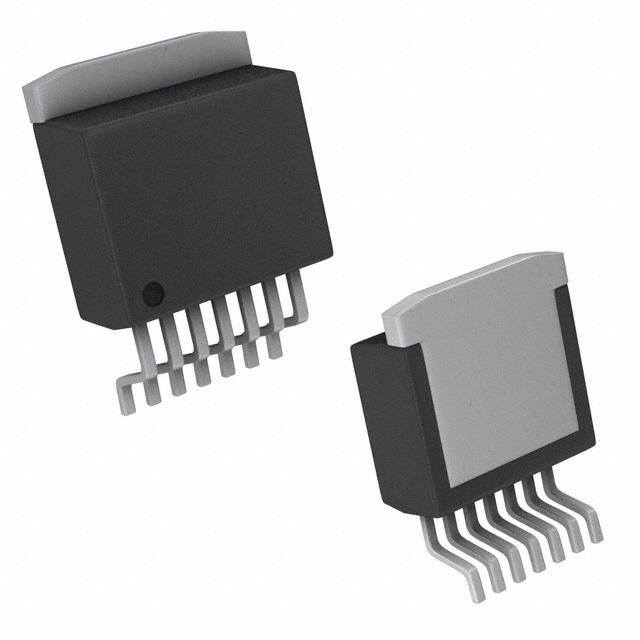
ICGOO电子元器件商城为您提供PA340CC由Apex Microtechnology Corporation设计生产,在icgoo商城现货销售,并且可以通过原厂、代理商等渠道进行代购。 PA340CC价格参考。Apex Microtechnology CorporationPA340CC封装/规格:线性 - 放大器 - 仪表,运算放大器,缓冲器放大器, 功率 放大器 1 电路 DDPAK-7。您可以下载PA340CC参考资料、Datasheet数据手册功能说明书,资料中有PA340CC 详细功能的应用电路图电压和使用方法及教程。
Apex Microtechnology的PA340CC是一款高性能运算放大器,属于线性放大器中的精密放大器类别。该器件主要应用于对精度、稳定性和带宽要求较高的场合。

典型应用场景包括:

1. 工业自动化与控制系统:用于传感器信号的高精度放大和处理,如温度、压力、流量等模拟信号的调理电路中。

2. 测试与测量设备:在示波器、信号发生器、万用表等仪器中作为前置放大器或中间级放大器,提供高增益和低噪声性能。

3. 医疗电子设备:如心电图机、监护仪等,用于生物电信号的放大处理,因其具备良好的共模抑制比和低偏置电流特性。

4. 音频处理系统:用于高保真音频放大器中,提供低失真和高动态范围的信号放大。

5. 电源管理系统:在高精度电压调节和电流检测电路中作为误差放大器使用。

PA340CC具备高带宽、低输入偏置电流和优良的温度稳定性,适合需要高性能模拟信号处理的应用环境。
| 参数 | 数值 |
| -3db带宽 | - |
| 产品目录 | 集成电路 (IC) |
| 描述 | IC OPAMP POWER 10MHZ DDPAK-7 |
| 产品分类 | Linear - Amplifiers - Instrumentation, OP Amps, Buffer Amps |
| 品牌 | Apex Microtechnology |
| 数据手册 | |
| 产品图片 |
|
| 产品型号 | PA340CC |
| rohs | 无铅 / 符合限制有害物质指令(RoHS)规范要求 |
| 产品系列 | Apex Precision Power® |
| 产品培训模块 | http://www.digikey.cn/PTM/IndividualPTM.page?site=cn&lang=zhs&ptm=30464 |
| 供应商器件封装 | DDPAK-7 |
| 其它名称 | 598-1917 |
| 包装 | 管件 |
| 压摆率 | 32 V/µs |
| 增益带宽积 | 10MHz |
| 安装类型 | 表面贴装 |
| 封装/外壳 | TO-263-8,D²Pak(7 引线+接片),TO-263CA |
| 工作温度 | -25°C ~ 85°C |
| 放大器类型 | 功率 |
| 标准包装 | 50 |
| 特色产品 | http://www.digikey.com/product-highlights/cn/zh/cirrus-logic-hv-power-op-amp/994 |
| 电压-电源,单/双 (±) | 20 V ~ 350 V, ±10 V ~ 175 V |
| 电压-输入失调 | 12mV |
| 电流-电源 | 2.2mA |
| 电流-输入偏置 | 50pA |
| 电流-输出/通道 | 120mA |
| 电路数 | 1 |
| 输出类型 | - |


- 商务部:美国ITC正式对集成电路等产品启动337调查
- 曝三星4nm工艺存在良率问题 高通将骁龙8 Gen1或转产台积电
- 太阳诱电将投资9.5亿元在常州建新厂生产MLCC 预计2023年完工
- 英特尔发布欧洲新工厂建设计划 深化IDM 2.0 战略
- 台积电先进制程称霸业界 有大客户加持明年业绩稳了
- 达到5530亿美元!SIA预计今年全球半导体销售额将创下新高
- 英特尔拟将自动驾驶子公司Mobileye上市 估值或超500亿美元
- 三星加码芯片和SET,合并消费电子和移动部门,撤换高东真等 CEO
- 三星电子宣布重大人事变动 还合并消费电子和移动部门
- 海关总署:前11个月进口集成电路产品价值2.52万亿元 增长14.8%


PDF Datasheet 数据手册内容提取
PAP3A43400 PA340 High Voltage Power Operational Amplifier FEATURES DESCRIPTION ♦ RoHS COMPLIANT The PA340 is a high voltage monolithic MOSFET oper- ♦ MONOLITHIC MOS TECHNOLOGY ational amplifier achieving performance features previ- ously found only in hybrid designs while increasing re- ♦ LOW COST liability. Inputs are protected from excessive common ♦ HIGH VOLTAGE OPERATION – 350V mode and differential mode voltages. The safe operat- ♦ LOW QUIESCENT CURRENT TYP. – 2.2mA ing area (SOA) has no second breakdown limitations. ♦ NO SECOND BREAKDOWN External compensation provides the user flexibility in ♦ HIGH OUTPUT CURRENT – 120 mA PEAK choosing optimum gain and bandwidth for the applica- tion. APPLICATIONS The surface mount package of the PA340CC is an in- ♦ TELEPHONE RING GENERATOR dustry standard non-hermetic plastic 7-pin DDPAK. ♦ PIEZO ELECTRIC POSITIONING ♦ ELECTROSTATIC TRANSDUCER & DEFLECTION ♦ DEFORMABLE MIRROR FOCUSING ♦ PACKAGING OPTIONS 7-pin DDPAK Surface Mount Package (PA340CC) FIGURE 1: Equivalent Schematic 3 +V D1 S Q1 Q2 Q3 I OUT 5 Q4 Q5 1 6 Q6 –IN COMP D2 D3 D4 D5 COMP Q8 2 7 +IN Q11 Q10 Q12 Q13 Q14 –V S 4 SUB Copyright © Apex Microtechnology, Inc. 2012 OCT 2013 www.apexanalog.com PA340U (All Rights Reserved) PA340U REVC1
PA340 High voltage considerations should be taken when designing board layouts for the PA340. The PA340 may require a derate in supply voltage depending on the spacing used for board layout. The 14-mil minimum spacing of the 7-pin DDPAK is adequate to standoff the 350V rating of the PA340. However, a supply voltage derate to 250V is required if the spacing of circuit board artwork is less than 11 mils. The metal tab of the PA340CC package is directly tied to -Vs. PA340CX TYPICAL APPLICATION PA340CC A A 1 1 DDPAK PKG. STYLE CC -IN +IN +Vs -Vs OUT P (Cc) P (Cc) MM OO CC FNoort eC: CC va mluuesst, bsee er agtreadp fho ro nfu pll asguep p4l.y volta-IN g+IN e.+Vs -Vs OUT P (Cc) P (Cc) C MM OO FIGURE 2. External Connections. CC Ref: APPLICATION NOTE 20: "Bridge Mode Operation of Power Amplifiers" Two PA340 amplifiers operated as a bridge driver for a piezo transducer provides a low cost 660 volt total drive capability. The R C network serves to raise the apparent gain of A2 at high frequencies. If R is set equal to R the N N N amplifiers can be compensated identically and will have matching bandwidths. R 20R 20R 20R V IN +175 +175 CC CC 10pF 10pF A1 A2 PA340 PA340 R N PIEZO TRANSDUCER C N LOW COST 660V p-p PIEZO DRIVER –175 –175 FIGURE 3. Low Cost 660V Piezo Driver P-P 2 PA340U
PA340 1. CHARACTERISTICS AND SPECIFICATIONS ABSOLUTE MAXIMUM RATINGS Parameter Symbol Min Max Units SUPPLY VOLTAGE, +V to -V 350 V S S OUTPUT CURRENT, continuous within SOA 60 mA OUTPUT CURRENT, peak (Note 3) 120 mA POWER DISSIPATION, continuous @ T = 25°C 14 W C INPUT VOLTAGE, differential -16 +16 V INPUT VOLTAGE, common mode -V +V V S S TEMPERATURE, pin solder - 10 sec 220 °C TEMPERATURE, junction (Note 2) 150 °C TEMPERATURE, storage -65 150 °C TEMPERATURE RANGE, powered (case) -40 125 °C SPECIFICATIONS (PER AMPLIFIER) Parameter Test Conditions (Note 1) Min Typ Max Units INPUT OFFSET VOLTAGE, initial 12 40 mV OFFSET VOLTAGE, vs. temperature 25°C to 85°C 17 250 µV/°C (Note 3) OFFSET VOLTAGE, vs. temperature -25°C to 25°C 18 500 µV/°C (Note 3) OFFSET VOLTAGE, vs. supply 4.5 µV/V OFFSET VOLTAGE, vs. time 80 µV/kh BIAS CURRENT, initial 50 200 pA BIAS CURRENT, vs. supply 2 pA/V OFFSET CURRENT, initial 50 200 pA INPUT IMPEDANCE, DC 1011 Ω INPUT CAPACITANCE 3 pF COMMON MODE, voltage range +V - 12 V S COMMON MODE, voltage range -V + 12 V S COMMON MODE REJECTION, DC V = ±90VDC 84 115 dB CM NOISE, broad band 10kHz BW, R = 1KΩ 337 µV RMS S GAIN OPEN LOOP at 15Hz R = 5KΩ 90 103 dB L GAIN BANDWIDTH PRODUCT @1MHz 10 MHz POWER BANDWIDTH 280V p-p 35 kHz PA340U 3
PA340 Parameter Test Conditions (Note 1) Min Typ Max Units OUTPUT VOLTAGE SWING I = 40mA ±V 12 ±V 10 V O S S CURRENT, peak (Note 3) 120 mA CURRENT, continuous 60 mA SETTLING TIME to 0.1% 10V step, A = -10 2 µs V SLEW RATE C = 4.7pF 32 V/µS C RESISTANCE, 10mA (Note 4) R = 0Ω 91 Ω CL RESISTANCE, 40mA (Note 4) R = 0Ω 65 Ω CL POWER SUPPLY VOLTAGE ±10 ±150 ±175 V CURRENT, quiescent 2.2 2.5 mA THERMAL RESISTANCE, AC junction to case F > 60Hz 5.9 6.85 °C/W RESISTANCE, DC junction to case F < 60Hz 7.7 8.9 °C/W RESISTANCE, junction to air Full temperature range 27 °C/W (Note 5) TEMPERATURE RANGE, case Meets full range specifications -25 25 +85 °C NOTES: 1. Unless otherwise noted T = 25°C, C = 6.8pF. DC input specifications are ± value given. Power sup- C C ply voltage is typical rating. 2. Long term operation at the maximum junction temperature will result in reduced product life. Derate internal power dissipation to achieve high MTTF. For guidance, refer to heatsink data sheet. 3. Guaranteed but not tested. 4. Since the PA340 has no current limit, load impedance must be large enough to limit output current to 120mA. 5. Heat tab attached to 3/32" FR-4 board with 2oz. copper. Topside copper area (heat tab directly at- tached) = 1000 sq. mm, backside copper area = 2500 sq. mm, board area = 2500 sq. mm. CAUTION The PA340 is constructed from MOSFET transistors. ESD handling procedures must be observed. 4 PA340U
PA340 2. TYPICAL PERFORMANCE GRAPHS W) POWER DERATING OUTPUT VOLTAGE SWING GAIN AND COMPENSATION P( 16 30 100 R DISSIPATION, 1110824 ROM V, (V)S 122505 VDROP-@8V5D°CROP+@85°C NSATION, pF 10 25°C55°C12855°C°C OWE 6 FROP 10 VDROP-@27°C MPE 1 AL P 4 VD 5 CO N 2 R VDROP+@27°C TE 0 0 0.1 N 0 25 50 75 100 125 0 20 40 60 80 100 120 0.1 1 10 I TEMPERATURE, T (°C) OUTPUT CURRENT, I (mA) GAIN O SMALL SIGNAL RESPONSE PHASE RESPONSE POWER RESPONSE -80 1000 AIN, A (dB)1680000 0.75pF2.2pF Φ (°)---111-90210000 0.75p2F.2pF 68pF E, (V) (p-p)OUT 2.26p.F8p1F5pF OOP G 40 6.8p1F5pF HASE, --113400 6.8pF OLTAG 100 33p6F8pF N L 20 68pF P-150 15pF T V E U P -160 P O 0 T -170 U O -20 -180 10 10 100 1K 10K 100K 1M 10M 10K 100K 1M 10M 10K 100K 1M FREQUENCY, F (Hz) FREQUENCY, F (Hz) FREQUENCY, F (Hz) HARMONIC DISTORTION SLEW RATE %) QUIESCENT CURRENT 10 (Q T, I 30 N102 E %) 1 RR ORTION, ( 0.1 180V6P-0PVP-3P0VP-P TE, (V/µs) 20 FALL SCENT CU100 1 2 5°2C5°C DIST0.01 A V = 20 LEW RA 10 RISE ED QUIE 98 -40°C C = 15pF S Z C LI R = 2K A L M 0.001 0 R 96 100 1K 10K 100K 5 15 25 35 45 55 65 75 85 O 20 60100140180220260300340 N FREQUENCY, F (Hz) COMPENSATION CAPACITANCE, C (pF) TOTAL SUPPLY VOLTAGE, (V) C COMMON MODE REJECTION POWER SUPPLY REJECTION CMR (dB)110200 PSR (dB) 19000 POSITIVE N, N, O O TI 80 TI 80 C C E E EJ 60 EJ 70 NEGATIVE R R E Y MOD 40 UPPL 60 N S O 20 R 50 M E M W O O C 0 P 40 10 100 1K 10K 100K 10 100 1K 10K 100K FREQUENCY, F (Hz) FREQUENCY, F (Hz) PA340U 5
PA340 3. APPLICATION INFORMATION Please read Application Note 1 "General Operating Considerations" which covers stability, power supplies, heat sinking, mounting, current limit, SOA interpretation, and specification interpretation. Visit www.apexanalog.com for design tools that help automate tasks such as calculations for stability, internal power dissipation, current limit, heat sink selection, Apex Microtechnology's complete Application Notes library, Technical Seminar Workbook and Evaluation Kits. 3.1 PHASE COMPENSATION Open loop gain and phase shift both increase with increasing temperature. The PHASE COMPENSATION typical graph shows closed loop gain and phase compensation capacitor value relationships for four case temperatures. The curves are based on achieving a phase margin of 50°. Calculate the highest case temperature for the applica- tion (maximum ambient temperature and highest internal power dissipation) before choosing the compensation. Keep in mind that when working with small values of compensation, parasitics may play a large role in performance of the finished circuit. The compensation capacitor must be rated for at least the total voltage applied to the amplifier and should be a temperature stable type such as NPO or COG. 3.2 OTHER STABILITY CONCERNS There are two important concepts about closed loop gain when choosing compensation. They stem from the fact that while "gain" is the most commonly used term, β (the feedback factor) is really what counts when designing for stability. 1. Gain must be calculated as a non-inverting circuit (equal input and feedback resistors can provide a signal gain of -1, but for calculating offset errors, noise, and stability, this is a gain of 2). 2. Including a feedback capacitor changes the feedback factor or gain of the circuit. Consider R = 4.7k, R = 47k IN f for a gain of 11. Compensation of 4.7 to 6.8pF would be reasonable. Adding 33pF parallel to the 47K rolls off the circuit at 103kHz, and at 2MHz has reduced gain from 11 to roughly 1.5 and the circuit is likely to oscillate. As a general rule the DC summing junction impedance (parallel combination of the feedback resistor and all input resistors) should be limited to 5K ohms or less. The amplifier input capacitance of about 6pF, plus capacitance of connecting traces or wires and (if used) a socket will cause undesirable circuit performance and even oscillation if these resistances are too high. In circuits requiring high resistances, measure or estimate the total sum point ca- pacitance, multiply by R /R, and parallel R with this value. Capacitors included for this purpose are usually in the IN f f single digit pF range. This technique results in equal feedback factor calculations for AC and DC cases. It does not produce a roll off, but merely keeps β constant over a wide frequency range. Paragraph 6 of Application Note 19 details suitable stability tests for the finished circuit. 3.3 SAFE OPERATING AREA SOA The MOSFET output stage of the PA340 is not limited by second 1.0 breakdown considerations as in bipolar output stages. However A) there are still three distinct limitations: –V, (S 00..35 200mS R 0.2 1. Voltage withstand capability of the transistors. O 2. Current handling capability of the die metallization. V S 0.1 300mS + 3. Temperature of the output MOSFETS. M O 0.05 R DC, T = 25°C These limitations can be seen in the SOA (see Safe Operating Area T F 00..0023 C N graphs). Note that each pulse capability line shows a constant power E DC, T = 85°C R 0.01 C level (unlike second breakdown limitations where power varies with R U voltage stress). These lines are shown for a case temperature of C0.005 T 25°C. Pulse stress levels for other case temperatures can be calcu- U0.003 P T0.002 lated in the same manner as DC power levels at different tempera- U O tures. The output stage is protected against transient flyback by the 0.001 10 20 30 50 100 200300 500 1K parasitic diodes of the output stage MOSFET structure. However, SUPPLY TO OUTPUT DIFFERENTIAL, V - V , (V) for protection against sustained high energy flyback external fast- S O recovery diodes must be used. FIGURE 4. Safe Operating Area 6 PA340U
PA340 3.4 HEATSINKING The PA340CC 7-pin DDPAK surface mountable package has a large exposed integrated copper heatslug to which the monolithic amplifier is directly attached. The PA340CC requires surface mount techniques of heatsinking. A sol- der connection to a copper foil area as defined in Note 5 of Page 3 is recommended for circuit board layouts. This may be adequate heatsinking but the large number of variables suggests temperature measurements to be made on the top of the package. Do not allow the temperature to exceed 85°C. 3.5 OVERVOLTAGE PROTECTION Although the PA340 can withstand differential input voltages up to 16V, in +Vs Z1 some applications additional external protection may be needed. Differen- tial inputs exceeding 16V will be clipped by the protection circuitry. How- ever, if more than a few milliamps of current is available from the overload -IN +Vs source, the protection circuitry could be destroyed. For differential sources above 16V, adding series resistance limiting input current to 1mA will pre- Q1 Q2 OUT vent damage. Alternatively, 1N4148 signal diodes connected anti-parallel across the input pins is usually sufficient. In more demanding applications +IN where bias current is important, diode connected JFETs such as 2N4416 -Vs will be required. See Q1 and Q2 in Figure 5. In either case the differential input voltage will be clamped to 0.7V. This is sufficient overdrive to produce the maximum power bandwidth. Z2 -Vs In the case of inverting circuits where the +IN pin is grounded, the diodes FIGURE 5. Overvoltage Protection mentioned above will also afford protection from excessive common mode voltage. In the case of non-inverting circuits, clamp diodes from each input to each supply will provide protection. Note that these diodes will have substantial reverse bias voltage under normal operation and diode leakage will produce errors. Some applications will also need over-voltage protection devices connected to the power supply rails. Unidirectional zener diode transient suppressors are recommended. The zeners clamp transients to voltages within the power supply rating and also clamp power supply reversals to ground. Whether the zeners are used or not the system power supply should be evaluated for transient performance including power-on overshoot and power-off polarity reversals as well as line regulation. See Z1 and Z2 in Figure 5. NEED TECHNICAL HELP? CONTACT APEX SUPPORT! For all Apex Microtechnology product questions and inquiries, call toll free 800-546-2739 in North America. For inquiries via email, please contact apex.support@apexanalog.com. International customers can also request support by contacting their local Apex Microtechnology Sales Representative. To find the one nearest to you, go to www.apexanalog.com IMPORTANT NOTICE Apex Microtechnology, Inc. has made every effort to insure the accuracy of the content contained in this document. However, the information is subject to change without notice and is provided "AS IS" without warranty of any kind (expressed or implied). Apex Microtechnology reserves the right to make changes without further notice to any specifications or products mentioned herein to improve reliability. This document is the property of Apex Microtechnology and by furnishing this informa- tion, Apex Microtechnology grants no license, expressed or implied under any patents, mask work rights, copyrights, trademarks, trade secrets or other intellectual property rights. Apex Microtechnology owns the copyrights associated with the information contained herein and gives consent for copies to be made of the informa- tion only for use within your organization with respect to Apex Microtechnology integrated circuits or other products of Apex Microtechnology. This consent does not extend to other copying such as copying for general distribution, advertising or promotional purposes, or for creating any work for resale. APEX MICROTECHNOLOGY PRODUCTS ARE NOT DESIGNED, AUTHORIZED OR WARRANTED TO BE SUITABLE FOR USE IN PRODUCTS USED FOR LIFE SUPPORT, AUTOMOTIVE SAFETY, SECURITY DEVICES, OR OTHER CRITICAL APPLICATIONS. PRODUCTS IN SUCH APPLICATIONS ARE UNDER- STOOD TO BE FULLY AT THE CUSTOMER OR THE CUSTOMER’S RISK. Apex Microtechnology, Apex and Apex Precision Power are trademarks of Apex Microtechnolgy, Inc. All other corporate names noted herein may be trademarks of their respective holders. Copyright © Apex Microtechnology, Inc. 2012 OCT 2013 PwAw3w4.0aUp e xanalog .com (All Rights Reserved) PA340U REVC7