ICGOO在线商城 > 集成电路(IC) > 线性 - 放大器 - 仪表,运算放大器,缓冲器放大器 > AD624SD
 Datasheet下载
- 型号: AD624SD
- 制造商: Analog
- 库位|库存: xxxx|xxxx
- 要求:
| 数量阶梯 | 香港交货 | 国内含税 |
| +xxxx | $xxxx | ¥xxxx |
查看当月历史价格
查看今年历史价格
AD624SD产品简介:
ICGOO电子元器件商城为您提供AD624SD由Analog设计生产,在icgoo商城现货销售,并且可以通过原厂、代理商等渠道进行代购。 AD624SD价格参考¥670.78-¥670.78。AnalogAD624SD封装/规格:线性 - 放大器 - 仪表,运算放大器,缓冲器放大器, 仪表 放大器 1 电路 16-CDIP。您可以下载AD624SD参考资料、Datasheet数据手册功能说明书,资料中有AD624SD 详细功能的应用电路图电压和使用方法及教程。
AD624SD是由Analog Devices Inc.(亚德诺半导体公司)生产的一款高性能仪表放大器,广泛应用于需要高精度、低噪声和高共模抑制比(CMRR)的场景。以下是AD624SD的主要应用场景:

1. 医疗设备:在心电图(ECG)、脑电图(EEG)等生物医学信号采集系统中,AD624SD能够精确放大微弱的生物电信号,同时有效抑制环境噪声和干扰信号,确保数据的准确性和可靠性。

2. 工业自动化:用于传感器信号调理电路中,如温度、压力、位移等传感器输出信号的放大。AD624SD具有高输入阻抗和低偏置电流特性,适合处理各种类型的传感器信号,确保信号不失真。

3. 测试与测量仪器:在精密测量仪器中,如数字万用表、示波器等,AD624SD可以提供稳定的增益和良好的线性度,确保测量结果的准确性。其宽工作温度范围也使其适用于各种恶劣环境下的测试需求。

4. 音频处理:在专业音频设备中,AD624SD可用于麦克风前置放大器或线路电平信号的放大。它能够保持信号的纯净度,减少失真,提供高质量的音频输出。

5. 通信系统:在射频(RF)和模拟信号处理领域,AD624SD可以作为前端放大器,提高接收机的灵敏度,同时降低噪声对信号的影响,确保通信质量。

6. 汽车电子:在车载传感器和控制系统中,AD624SD能够处理来自各种传感器的信号,如车速传感器、加速度传感器等,确保车辆运行状态的实时监控和控制。

总之,AD624SD凭借其卓越的性能和稳定性,在多个领域中发挥着重要作用,特别是在需要高精度和可靠性的应用场合。
| 参数 | 数值 |
| -3db带宽 | 1MHz |
| 产品目录 | 集成电路 (IC)半导体 |
| 描述 | IC OPAMP INSTR 25MHZ 16CDIP仪表放大器 LOW NOISE HI PREC |
| 产品分类 | Linear - Amplifiers - Instrumentation, OP Amps, Buffer Amps集成电路 - IC |
| 品牌 | Analog Devices Inc |
| 产品手册 | |
| 产品图片 |
|
| rohs | 否不符合限制有害物质指令(RoHS)规范要求 |
| 产品系列 | 放大器 IC,仪表放大器,Analog Devices AD624SD- |
| 数据手册 | |
| 产品型号 | AD624SD |
| 产品培训模块 | http://www.digikey.cn/PTM/IndividualPTM.page?site=cn&lang=zhs&ptm=30008http://www.digikey.cn/PTM/IndividualPTM.page?site=cn&lang=zhs&ptm=26202 |
| 产品种类 | 仪表放大器 |
| 供应商器件封装 | 16-CDIP 侧面铜焊 |
| 共模抑制比—最小值 | 110 dB |
| 包装 | 管件 |
| 压摆率 | 5 V/µs |
| 双重电源电压 | +/- 18 V |
| 商标 | Analog Devices |
| 增益带宽生成 | 25 MHz |
| 增益带宽积 | 25MHz |
| 安装类型 | 通孔 |
| 安装风格 | Through Hole |
| 封装 | Tube |
| 封装/外壳 | 16-CDIP(0.300",7.62mm) |
| 封装/箱体 | CDIP-16 SB |
| 工作温度 | -55°C ~ 125°C |
| 工作温度范围 | - 55 C to + 125 C |
| 工作电源电压 | 12 V to 36 V |
| 工厂包装数量 | 23 |
| 带宽 | 150 kHz |
| 放大器类型 | 仪表 |
| 最大功率耗散 | 420 mW |
| 最大工作温度 | + 125 C |
| 最大输入电阻 | 1000 MOhms at +/- 15 V |
| 最小工作温度 | - 55 C |
| 标准包装 | 1 |
| 电压-电源,单/双 (±) | ±6 V ~ 18 V |
| 电压-输入失调 | 75µV |
| 电流-电源 | 3.5mA |
| 电流-输入偏置 | 50nA |
| 电流-输出/通道 | - |
| 电源电流 | 5 mA |
| 电路数 | 1 |
| 系列 | AD624 |
| 视频文件 | http://www.digikey.cn/classic/video.aspx?PlayerID=1364138032001&width=640&height=505&videoID=2245193153001http://www.digikey.cn/classic/video.aspx?PlayerID=1364138032001&width=640&height=505&videoID=2245193159001 |
| 转换速度 | 5 V/us |
| 输入偏压电流—最大 | 15 nA |
| 输入补偿电压 | 200 uV |
| 输出类型 | - |
| 通道数量 | 1 Channel |


- 商务部:美国ITC正式对集成电路等产品启动337调查
- 曝三星4nm工艺存在良率问题 高通将骁龙8 Gen1或转产台积电
- 太阳诱电将投资9.5亿元在常州建新厂生产MLCC 预计2023年完工
- 英特尔发布欧洲新工厂建设计划 深化IDM 2.0 战略
- 台积电先进制程称霸业界 有大客户加持明年业绩稳了
- 达到5530亿美元!SIA预计今年全球半导体销售额将创下新高
- 英特尔拟将自动驾驶子公司Mobileye上市 估值或超500亿美元
- 三星加码芯片和SET,合并消费电子和移动部门,撤换高东真等 CEO
- 三星电子宣布重大人事变动 还合并消费电子和移动部门
- 海关总署:前11个月进口集成电路产品价值2.52万亿元 增长14.8%


PDF Datasheet 数据手册内容提取
a Precision Instrumentation Amplifier AD624 FEATURES FUNCTIONAL BLOCK DIAGRAM Low Noise: 0.2(cid:1)V p-p 0.1 Hz to 10 Hz Low Gain TC:5 ppm max (G = 1) 50(cid:3) Low Nonlinearity: 0.001% max (G = 1 to 200) –INPUT High CMRR: 130 dB min (G = 500 to 1000) G = 100 AD624 Low Input Offset Voltage: 25(cid:1)V, max 225.3(cid:3) Low Input Offset Voltage Drift: 0.25(cid:1)V/(cid:2)C max G = 200 4445.7(cid:3) Gain Bandwidth Product: 25 MHz 124(cid:3) VB 10k(cid:3) Pin Programmable Gains of 1, 100, 200, 500, 1000 G = 500 SENSE No External Components Required 80.2(cid:3) 20k(cid:3) 10k(cid:3) Internally Compensated RG1 20k(cid:3) 10k(cid:3) OUTPUT RG2 10k(cid:3) REF 50(cid:3) +INPUT PRODUCT DESCRIPTION PRODUCT HIGHLIGHTS The AD624 is a high precision, low noise, instrumentation 1. The AD624 offers outstanding noise performance. Input amplifier designed primarily for use with low level transducers, noise is typically less than 4nV/√Hz at 1 kHz. including load cells, strain gauges and pressure transducers. An 2. The AD624 is a functionally complete instrumentation am- outstanding combination of low noise, high gain accuracy, low plifier. Pin programmable gains of 1, 100, 200, 500 and 1000 gain temperature coefficient and high linearity make the AD624 are provided on the chip. Other gains are achieved through ideal for use in high resolution data acquisition systems. the use of a single external resistor. The AD624C has an input offset voltage drift of less than 3. The offset voltage, offset voltage drift, gain accuracy and gain 0.25µV/°C, output offset voltage drift of less than 10µV/°C, temperature coefficients are guaranteed for all pretrimmed CMRR above 80dB at unity gain (130dB at G = 500) and a gains. maximum nonlinearity of 0.001% at G = 1. In addition to these 4. The AD624 provides totally independent input and output outstanding dc specifications, the AD624 exhibits superior ac performance as well. A 25MHz gain bandwidth product, 5V/µs offset nulling terminals for high precision applications. slew rate and 15µs settling time permit the use of the AD624 in This minimizes the effect of offset voltage in gain ranging applications. high speed data acquisition applications. 5. A sense terminal is provided to enable the user to minimize The AD624 does not need any external components for pre- the errors induced through long leads. A reference terminal is trimmed gains of 1, 100, 200, 500 and 1000. Additional gains also provided to permit level shifting at the output. such as 250 and 333 can be programmed within one percent accuracy with external jumpers. A single external resistor can also be used to set the 624’s gain to any value in the range of 1 to 10,000. REV. C Information furnished by Analog Devices is believed to be accurate and reliable. However, no responsibility is assumed by Analog Devices for its use, nor for any infringements of patents or other rights of third parties One Technology Way, P.O. Box 9106, Norwood, MA 02062-9106, U.S.A. which may result from its use. No license is granted by implication or Tel: 781/329-4700 www.analog.com otherwise under any patent or patent rights of Analog Devices. Fax: 781/326-8703 © Analog Devices, Inc., 1999
AD624–SPECIFICATIONS (@ V = (cid:4)15V, R = 2k(cid:3) and T = +25(cid:2)C, unless otherwise noted) S L A Model AD624A AD624B AD624C AD624S Min Typ Max Min Typ Max Min Typ Max Min Typ Max Units GAIN Gain Equation (External Resistor Gain Programming) 40,000 40,000 40,000 40,000 +1±20% +1±20% +1±20% +1±20% R R R R G G G G Gain Range (Pin Programmable) 1 to 1000 1 to 1000 1 to 1000 1 to 1000 Gain Error G = 1 ±0.05 ±0.03 ±0.02 ±0.05 % G = 100 ±0.25 ±0.15 ±0.1 ±0.25 % G = 200, 500 ±0.5 ±0.35 ±0.25 ±0.5 % Nonlinearity G = 1 ±0.005 ±0.003 ±0.001 ±0.005 % G = 100, 200 ±0.005 ±0.003 ±0.001 ±0.005 % G = 500 ±0.005 ±0.005 ±0.005 ±0.005 % Gain vs. Temperature G = 1 5 5 5 5 ppm/°C G = 100, 200 10 10 10 10 ppm/°C G = 500 25 15 15 15 ppm/°C VOLTAGE OFFSET (May be Nulled) Input Offset Voltage 200 75 25 75 µV vs. Temperature 2 0.5 0.25 2.0 µV/°C Output Offset Voltage 5 3 2 3 mV vs. Temperature 50 25 10 50 µV/°C OOffUsTet Referred to the Input vs. Supply G = 1 70 75 80 75 dB G = 100, 200 95 105 110 105 dB G = 500 100 110 115 110 dB INPUT CURRENT Input Bias Current ±50 ±25 ±15 ±50 nA vs. Temperature ±50 ±50 ±50 ±50 pA/°C Input Offset Current ±35 ±15 ±10 ±35 nA vs. Temperature ±20 ±20 ±20 ±20 pA/°C INPUT Input Impedance Differential Resistance 109 109 109 109 Ω Differential Capacitance 10 10 10 10 pF Common-Mode Resistance 109 109 109 109 Ω Common-Mode Capacitance 10 10 10 10 pF Input Voltage Range1 Max Differ. Input Linear (VDL) ±10 G ±10 G ±10 G ±10 G V Max Common-Mode Linear (VCM) 12 V− 2 ×VD 12 V− 2 ×VD 12 V− 2 ×VD 12 V− 2 ×VD V Common-Mode Rejection dc to 60 Hz with 1 kΩ Source Imbalance G = 1 70 75 80 70 dB G = 100, 200 100 105 110 100 dB G = 500 110 120 130 110 dB OUTPUT RATING V , R = 2 kΩ ±10 ±10 ±10 ±10 V L DYNAMIC RESPONSE Small Signal –3 dB G = 1 1 1 1 1 MHz G = 100 150 150 150 150 kHz G = 200 100 100 100 100 kHz G = 500 50 50 50 50 kHz G = 1000 25 25 25 25 kHz Slew Rate 5.0 5.0 5.0 5.0 V/µs Settling Time to 0.01%, 20 V Step G = 1 to 200 15 15 15 15 µs G = 500 35 35 35 35 µs G = 1000 75 75 75 75 µs NOISE Voltage Noise, 1 kHz R.T.I. 4 4 4 4 nV/√Hz R.T.O. 75 75 75 75 nV/√Hz R.T.I., 0.1 Hz to 10 Hz G = 1 10 10 10 10 µV p-p G = 100 0.3 0.3 0.3 0.3 µV p-p G = 200, 500, 1000 0.2 0.2 0.2 0.2 µV p-p Current Noise 0.1 Hz to 10 Hz 60 60 60 60 pA p-p SENSE INPUT R 8 10 12 8 10 12 8 10 12 8 10 12 kΩ IN I 30 30 30 30 µA IN Voltage Range ±10 ±10 ±10 ±10 V Gain to Output 1 1 1 1 % –2– REV. C
AD624 Model AD624A AD624B AD624C AD624S Min Typ Max Min Typ Max Min Typ Max Min Typ Max Units REFERENCE INPUT R 16 20 24 16 20 24 16 20 24 16 20 24 kΩ IN I 30 30 30 30 µA IN Voltage Range ±10 ±10 ±10 ±10 V Gain to Output 1 1 1 1 % TEMPERATURE RANGE Specified Performance –25 +85 –25 +85 –25 +85 –55 +125 °C Storage –65 +150 –65 +150 –65 +150 –65 +150 °C POWER SUPPLY (cid:4) (cid:4) (cid:4) (cid:4) (cid:4) (cid:4) (cid:4) (cid:4) (cid:4) (cid:4) (cid:4) (cid:4) Power Supply Range 6 15 18 6 15 18 6 15 18 6 15 18 V Quiescent Current 3.5 5 3.5 5 3.5 5 3.5 5 mA NOTES 1V is the maximum differential input voltage at G = 1 for specified nonlinearity, V at other gains = 10 V/G. V = actual differential input voltage. DL DL D 1Example: G = 10, V = 0.50. V = 12 V – (10/2 × 0.50 V) = 9.5 V. D CM Specifications subject to change without notice. Specifications shown in boldface are tested on all production unit at final electrical test. Results from those tests are used to calculate outgoing quality levels. All min and max specifications are guaranteed, although only those shown in boldface are tested on all production units. ABSOLUTE MAXIMUM RATINGS* CONNECTION DIAGRAM Supply Voltage . . . . . . . . . . . . . . . . . . . . . . . . . . . . . . . . ±18 V Internal Power Dissipation . . . . . . . . . . . . . . . . . . . . . 420 mW Input Voltage . . . . . . . . . . . . . . . . . . . . . . . . . . . . . . . . . . . ±VS –INPUT 1 16 RG1 Differential Input Voltage . . . . . . . . . . . . . . . . . . . . . . . . . ±V +INPUT 2 15 OUTPUT NULL S Output Short Circuit Duration . . . . . . . . . . . . . . . . Indefinite RG2 3 14 OUTPUT NULL Storage Temperature Range . . . . . . . . . . . . . –65°C to +150°C INPUT NULL 4 AD624 13 G = 100 SHORT TO Operating Temperature Range INPUT NULL 5 (NToOt Pto V SIEcaWle) 12 G = 200 RG2 FOR AD624A/B/C . . . . . . . . . . . . . . . . . . . . . . . –25°C to +85°C DESIRED REF 6 11 G = 500 GAIN AD624S . . . . . . . . . . . . . . . . . . . . . . . . . . . –55°C to +125°C Lead Temperature (Soldering, 60 secs) . . . . . . . . . . . . +300°C –VS 7 10 SENSE +VS 8 9 OUTPUT *Stresses above those listed under Absolute Maximum Ratings may cause perma- nent damage to the device. This is a stress rating only; functional operation of the FOR GAINS OF 1000 SHORT RG1 TO PIN 12 device at these or any other conditions above those indicated in the operational AND PINS 11 AND 13 TO RG2 sections of this specification is not implied. Exposure to absolute maximum rating conditions for extended periods may affect device reliability. METALIZATION PHOTOGRAPH Contact factory for latest dimensions ORDERING GUIDE Dimensions shown in inches and (mm). Temperature Package Package Model Range Description Option AD624AD –25°C to +85°C 16-Lead Ceramic DIP D-16 AD624BD –25°C to +85°C 16-Lead Ceramic DIP D-16 AD624CD –25°C to +85°C 16-Lead Ceramic DIP D-16 AD624SD –55°C to +125°C 16-Lead Ceramic DIP D-16 AD624SD/883B* –55°C to +125°C 16-Lead Ceramic DIP D-16 AD624AChips –25°C to +85°C Die AD624SChips –25°C to +85°C Die *See Analog Devices’ military data sheet for 883B specifications. REV. C –3–
AD624–Typical Characteristics 20 20 30 (cid:4)E – V15 (cid:4)NG – V15 G – V p-p INPUT VOLTAGE RANG150 +25(cid:2)C OUTPUT VOLTAGE SWI150 OUTPUT VOLTAGE SWIN2100 0 0 0 0 5 10 15 20 0 5 10 15 20 10 100 1k 10k SUPPLY VOLTAGE – (cid:4)V SUPPLY VOLTAGE – (cid:4)V LOAD RESISTANCE – (cid:3) Figure 1.Input Voltage Range vs. Figure 2.Output Voltage Swing vs. Figure 3.Output Voltage Swing vs. Supply Voltage, G = 1 Supply Voltage Load Resistance 8.0 16 40 A m – 14 30 PLIFIER QUIESCENT CURRENT 624...000 (cid:4)INPUT BIAS CURRENT – nA11428602 INPUT BIAS CURRENT – nA –––23112000000 M A 0 0 –40 0 5 10 15 20 0 5 10 15 20 –125 –75 –25 25 75 125 SUPPLY VOLTAGE – (cid:4)V SUPPLY VOLTAGE – (cid:4)V TEMPERATURE – (cid:2)C Figure 4.Quiescent Current vs. Figure 5.Input Bias Current vs. Figure 6.Input Bias Current vs. Supply Voltage Supply Voltage Temperature 16 –1 14 A V 0 n (cid:1) (cid:4)T – 12 UE – 1 500 S CURREN 180 FINAL VAL 32 AIN – V/V10100 BIA 6 OM 4 G T R 1 PU 4 S F 5 N O I V 2 (cid:5) 6 0 0 0 5 10 15 20 7 1 10 100 1k 10k 100k 1M 10M INPUT VOLTAGE – (cid:4)V 0 1.0 2.0 3.0 4.0 5.0 6.0 7.0 8.0 FREQUENCY – Hz WARM-UP TIME – Minutes Figure 7.Input Bias Current vs. CMV Figure 8.Offset Voltage, RTI, Turn Figure 9.Gain vs. Frequency On Drift –4– REV. C
AD624 –140 30 160 G = 500 CMRR – dB––1–––10286400000 GG = = 1 010 LL-POWER RESPONSE – V p-p2100 G G= 1=0 50000 G =G 1 ,= 1 10000 - WER SUPPLY REJECTION – dB111486024000000 G = 500 G G–1=VV 1= Sp0 1=0-p – S1I5NVE dWcA+VE –20 FU BANDWIDTH LIMITED PO 20 0 0 0 1 10 100 1k 10k 100k 1M 10M 1k 10k 100k 1M 10 100 1k 10k 100k FREQUENCY – Hz FREQUENCY – Hz FREQUENCY – Hz Figure 10.CMRR vs. Frequency RTI, Figure 11.Large Signal Frequency Figure 12.Positive PSRR vs. Zero to 1k Source Imbalance Response Frequency 1000 160 Hz100k ON – dB112400 G = 500 –1VVS p =-p – S1I5NVE dWcA+VE Hz 100 G = 1 SITY – fA/ 10k WER SUPPLY REJECTI148600000 GG = = 1 100 VOLT NSD – nV/ 110 G = G10 =0 ,1 10000 G = 1000 NOISE SPECTRAL DEN1010000 PO 20 NT E 0 0.1 RR 10 10 100 1k 10k 100k 1 10 100 1k 10k 100k CU 0.1 1 10 100 10k 100k FREQUENCY – Hz FREQUENCY – Hz FREQUENCY – Hz Figure 13.Negative PSRR vs. Figure 14.RTI Noise Spectral Figure 15.Input Current Noise Frequency Density vs. Gain –12 TO 12 1% 0.1% 0.01% –8 TO 8 –4 TO 4 OUTPUT STEP –V 4 TO –4 8 TO –8 1% 0.1% 0.01% 12 TO –12 0 5 10 15 20 SETTLING TIME – (cid:1)s Figure 16.Low Frequency Voltage Figure 17.Low Frequency Voltage Figure 18.Settling Time, Gain = 1 NoiseG = 1 (System Gain = 1000) Noise, G = 1000 (System Gain = , 100,000) REV. C –5–
AD624 –12 TO 12 0.1% 1% 0.01% –8 TO 8 –4 TO 4 OUTPUT STEP –V 4 TO –4 8 TO –8 1% 0.1% 0.01% 12 TO –12 0 5 10 15 20 SETTLING TIME – (cid:1)s Figure 19.Large Signal Pulse Figure 20.Settling Time Gain = 100 Figure 21.Large Signal Pulse Response and Settling Time, G = 1 Response and Settling Time, G = 100 –12 TO 12 1% 0.1% 0.01% –8 TO 8 –4 TO 4 OUTPUT STEP –V 4 TO –4 8 TO –8 0.01% 12 TO –12 1% 0.1% 0 5 10 15 20 SETTLING TIME – (cid:1)s Figure 22.Range Signal Pulse Figure 23.Settling Time Gain = 1000 Figure 24.Large Signal Pulse Response and Settling Time, Response and Settling Time, G = 500 G = 1000 –6– REV. C
AD624 10k(cid:3) 1k(cid:3) 10k(cid:3) 1% 10T 1% 2I0NVP Up-Tp 100k(cid:3) +VS VOUT 1% RG1 G = 100 G = 200 AD624 G = 500 1k(cid:3) 500(cid:3) 200(cid:3) 0.1% 0.1% 0.1% RG2 –VS Figure 25. Settling Time Test Circuit THEORY OF OPERATION The AD524 should be considered in applications that require The AD624 is a monolithic instrumentation amplifier based on protection from severe input overload. If this is not possible, a modification of the classic three-op-amp instrumentation external protection resistors can be put in series with the inputs amplifier. Monolithic construction and laser-wafer-trimming of the AD624 to augment the internal (50Ω) protection resis- allow the tight matching and tracking of circuit components and tors. This will most seriously degrade the noise performance. the high level of performance that this circuit architecture is ca- For this reason the value of these resistors should be chosen to pable of. be as low as possible and still provide 10mA of current limiting under maximum continuous overload conditions. In selecting A preamp section (Q1–Q4) develops the programmed gain by the value of these resistors, the internal gain setting resistor and the use of feedback concepts. Feedback from the outputs of A1 the 1.2 volt drop need to be considered. For example, to pro- and A2 forces the collector currents of Q1–Q4 to be constant tect the device from a continuous differential overload of 20V thereby impressing the input voltage across R . G at a gain of 100, 1.9kΩ of resistance is required. The internal The gain is set by choosing the value of RG from the equation, gain resistor is 404Ω; the internal protect resistor is 100Ω. 40k There is a 1.2V drop across D1 or D2 and the base-emitter Gain = + 1. The value of R also sets the transconduct- R G junction of either Q1 and Q3 or Q2 and Q4 as shown in Figure G ance of the input preamp stage increasing it asymptotically to 27, 1400Ω of external resistance would be required (700Ω in the transconductance of the input transistors as R is reduced series with each input). The RTI noise in this case would be G for larger gains. This has three important advantages. First, this approach allows the circuit to achieve a very high open loop gain 4KTRext+(4nV/ Hz)2 =6.2nV/ Hz of 3 × 10⁸ at a programmed gain of 1000 thus reducing gain related errors to a negligible 3 ppm. Second, the gain bandwidth +VS pcorondduucctt awnhciec,h r eisa cdheetse r2m5inMedH bz.y T Ch3ir odr, Cth4e ainnpdu tth veo ilntapguet ntroainses- I510(cid:1)A VB I520(cid:1)A 1R05k2(cid:3) SENSE reduces to a value determined by the collector current of the A1 A2 input transistors for an RTI noise of 4 nV/√Hz at G ≥ 500. C3 C4 R53 10k(cid:3) +VS R57 A3 VO 50(cid:3) 20k(cid:3) Q1, Q3 R56 Q2, R54 100 +VS –IN RG1 RG2 20k(cid:3) Q4 10k(cid:3) R55 R25G00002 AD624 116(cid:1).2Fk(cid:3) AD1/72192.09k(cid:3)1(cid:1)F AD1/7212 50(cid:1)1A3 4445(cid:3) 8102.24(cid:3)(cid:3) 250000 50(cid:1)IA4 50(cid:3)10k(cid:3) REF 16.2k(cid:3) 225.3(cid:3) +IN G500 G1, 100, 200 1(cid:1)F 100 –VS 1k(cid:3) –VS 100(cid:3) –VS 1.62M(cid:3) 1.82k(cid:3) Figure 27.Simplified Circuit of Amplifier; Gain Is Defined as (R56 + R57)/(R) + 1. For a Gain of 1, R Is an Open G G Figure 26.Noise Test Circuit Circuit. INPUT CONSIDERATIONS INPUT OFFSET AND OUTPUT OFFSET Under input overload conditions the user will see R + 100Ω Voltage offset specifications are often considered a figure of G and two diode drops (~1.2V) between the plus and minus merit for instrumentation amplifiers. While initial offset may inputs, in either direction. If safe overload current under all be adjusted to zero, shifts in offset voltage due to temperature conditions is assumed to be 10mA, the maximum overload variations will cause errors. Intelligent systems can often correct voltage is ~ ±2.5V. While the AD624 can withstand this con- for this factor with an autozero cycle, but there are many small- tinuously, momentary overloads of ±10V will not harm the signal high-gain applications that don’t have this capability. device. On the other hand the inputs should never exceed the Voltage offset and offset drift each have two components; input supply voltage. and output. Input offset is that component of offset that is REV. C –7–
AD624 directly proportional to gain i.e., input offset as measured at Table I. theoutput at G = 100 is 100 times greater than at G = 1. Temperature Outputoffset is independent of gain. At low gains, output offset Gain Coefficient Pin 3 drift isdominant, while at high gains input offset drift domi- (Nominal) (Nominal) to Pin Connect Pins nates.Therefore, the output offset voltage drift is normally specifiedas drift at G = 1 (where input effects are insignificant), 1 –0 ppm/°C – – whileinput offset voltage drift is given by drift specification at a 100 –1.5 ppm/°C 13 – highgain (where output offset effects are negligible). All input- 125 –5 ppm/°C 13 11 to 16 relatednumbers are referred to the input (RTI) which is to say 137 –5.5 ppm/°C 13 11 to 12 that theeffect on the output is “G” times larger. Voltage offset 186.5 –6.5 ppm/°C 13 11 to 12 to 16 vs. powersupply is also specified at one or more gain settings 200 –3.5 ppm/°C 12 – and is alsoRTI. 250 –5.5 ppm/°C 12 11 to 13 333 –15 ppm/°C 12 11 to 16 By separating these errors, one can evaluate the total error inde- 375 –0.5 ppm/°C 12 13 to 16 pendent of the gain setting used. In a given gain configura- 500 –10 ppm/°C 11 – tionboth errors can be combined to give a total error referred to 624 –5 ppm/°C 11 13 to 16 theinput (R.T.I.) or output (R.T.O.) by the following formula: 688 –1.5 ppm/°C 11 11 to 12; 13 to 16 Total Error R.T.I. = input error + (output error/gain) 831 +4 ppm/°C 11 16 to 12 Total Error R.T.O. = (Gain × input error) + output error 1000 0 ppm/°C 11 16 to 12; 13 to 11 As an illustration, a typical AD624 might have a +250µV out- Pins 3 and 16 programs the gain according to the formula putoffset and a –50µV input offset. In a unity gain configura- 40k tion,the total output offset would be 200µV or the sum of the R = two.At a gain of 100, the output offset would be –4.75mV G G−1 or:+250µV + 100 (–50µV) = –4.75mV. (see Figure 29). For best results RG should be a precision resis- tor with a low temperature coefficient. An external R affects both G The AD624 provides for both input and output offset adjust- gain accuracy and gain drift due to the mismatch between it and ment.This optimizes nulling in very high precision applications the internal thin-film resistors R56 and R57. Gain accuracy is andminimizes offset voltage effects in switched gain applica- determined by the tolerance of the external R and the absolute G tions. Insuch applications the input offset is adjusted first at the accuracy of the internal resistors (±20%). Gain drift is determined highestprogrammed gain, then the output offset is adjusted at by the mismatch of the temperature coefficient of R and the tem- G G = 1. perature coefficient of the internal resistors (–15ppm/°C typ), and the temperature coefficient of the internal interconnections. GAIN The AD624 includes high accuracy pretrimmed internal +VS gainresistors. These allow for single connection program- –INPUT ming ofgains of 1, 100, 200 and 500. Additionally, a variety RG1 1.5k(cid:3) of gainsincluding a pretrimmed gain of 1000 can be achieved throughseries and parallel combinations of the internal resis- 1k(cid:3) OR 2.105k(cid:3) AD624 VOUT tors. Table Ishows the available gains and the appropriate RG2 REFERENCE pin connectionsand gain temperature coefficients. +INPUT The gain values achieved via the combination of internal –VS G = 4 2 0 . .1 0 0 0 5 0 + 1 = 20 (cid:4)20% resistorsare extremely useful. The temperature coefficient of the Figure 29.Operating Connections for G = 20 gain isdependent primarily on the mismatch of the temperature The AD624 may also be configured to provide gain in the out- coefficients of the various internal resistors. Tracking of these put stage. Figure 30 shows an H pad attenuator connected to resistorsis extremely tight resulting in the low gain TCs shown the reference and sense lines of the AD624. The values of R1, inTable I. R2 and R3 should be selected to be as low as possible to mini- If the desired value of gain is not attainable using the inter- mize the gain variation and reduction of CMRR. Varying R2 nalresistors, a single external resistor can be used to achieve will precisely set the gain without affecting CMRR. CMRR is anygain between 1 and 10,000. This resistor connected between determined by the match of R1 and R3. +VS IONFPFUSTET +VS R1 –INPUT 10k(cid:3) NULL –INPUT 6k(cid:3) RG1 RG1 R2 G = 100 G = 100 5k(cid:3) G = 200 AD624 VOUT G = 200 AD624 VOUT G = 500 G = 500 RL OUTPUT RG2 SIGNAL RG2 +INPUT COMMON +INPUT R3 –VS –VS 6k(cid:3) Figure 28.Operating Connections for G = 200 G = (R2||2(0Rk2(cid:3)||2) 0+k R(cid:3)1) + R3) (R1 + R2 + R3) || RL 2k(cid:3) Figure 30.Gain of 2500 –8– REV. C
AD624 NOISE +VS The AD624 is designed to provide noise performance near the theoretical noise floor. This is an extremely important design criteria as the front end noise of an instrumentation amplifier is the ultimate limitation on the resolution of the data acquisition AD624 system it is being used in. There are two sources of noise in an LOAD instrument amplifier, the input noise, predominantly generated by the differential input stage, and the output noise, generated by the output amplifier. Both of these components are present –VS TPOOWER SUPPLY at the input (and output) of the instrumentation amplifier. At GROUND the input, the input noise will appear unaltered; the output c.AC-Coupled noise will be attenuated by the closed loop gain (at the output, the output noise will be unaltered; the input noise will be ampli- Figure 31.Indirect Ground Returns for Bias Currents fied by the closed loop gain). Those two noise sources must be Although instrumentation amplifiers have differential inputs, root sum squared to determine the total noise level expected at there must be a return path for the bias currents. If this is not the input (or output). provided, those currents will charge stray capacitances, causing The low frequency (0.1Hz to 10Hz) voltage noise due to the the output to drift uncontrollably or to saturate. Therefore, output stage is 10µV p-p, the contribution of the input stage is when amplifying “floating” input sources such as transformers 0.2µV p-p. At a gain of 10, the RTI voltage noise would be and thermocouples, as well as ac-coupled sources, there must still be a dc path from each input to ground, (see Figure 31). 1µV p-p, 102+(0.2)2 . The RTO voltage noise would be G COMMON-MODE REJECTION Common-mode rejection is a measure of the change in output 10.2µV p-p, 102+(0.2(G))2. These calculations hold for voltage when both inputs are changed by equal amounts. These specifications are usually given for a full-range input voltage applications using either internal or external gain resistors. change and a specified source imbalance. “Common-Mode Rejection Ratio” (CMRR) is a ratio expression while “Common- INPUT BIAS CURRENTS Mode Rejection” (CMR) is the logarithm of that ratio. For Input bias currents are those currents necessary to bias the input example, a CMRR of 10,000 corresponds to a CMR of 80dB. transistors of a dc amplifier. Bias currents are an additional source of input error and must be considered in a total error In an instrumentation amplifier, ac common-mode rejection is budget. The bias currents when multiplied by the source resis- only as good as the differential phase shift. Degradation of ac tance imbalance appear as an additional offset voltage. (What is common-mode rejection is caused by unequal drops across of concern in calculating bias current errors is the change in bias differing track resistances and a differential phase shift due to current with respect to signal voltage and temperature.) Input varied stray capacitances or cable capacitances. In many appli- offset current is the difference between the two input bias cur- cations shielded cables are used to minimize noise. This tech- rents. The effect of offset current is an input offset voltage whose nique can create common-mode rejection errors unless the magnitude is the offset current times the source resistance. shield is properly driven. Figures 32 and 33 shows active data guards which are configured to improve ac common-mode +VS rejection by “bootstrapping” the capacitances of the input cabling, thus minimizing differential phase shift. +VS –INPUT AD624 LOAD G = 200 100(cid:3) RG2 AD624 VOUT –VS TPOOWER AD711 REFERENCE SUPPLY GROUND +INPUT a.Transformer Coupled –VS Figure 32.Shield Driver, G ≥ 100 +VS +VS –INPUT 100(cid:3) AD712 RG1 AD624 AD624 VOUT LOAD 100(cid:3) –VS RG2 REFERENCE +INPUT –VS TPSOOUPWPELRY –VS GROUND Figure 33.Differential Shield Driver b.Thermocouple REV. C –9–
AD624 GROUNDING “inside the loop” of an instrumentation amplifier to provide the Many data-acquisition components have two or more ground required current without significantly degrading overall perfor- pins which are not connected together within the device. These mance. The effects of nonlinearities, offset and gain inaccuracies grounds must be tied together at one point, usually at the sys- of the buffer are reduced by the loop gain of the IA output tem power supply ground. Ideally, a single solid ground would amplifier. Offset drift of the buffer is similarly reduced. be desirable. However, since current flows through the ground wires and etch stripes of the circuit cards, and since these paths REFERENCE TERMINAL have resistance and inductance, hundreds of millivolts can be The reference terminal may be used to offset the output by up generated between the system ground point and the data acqui- to ±10V. This is useful when the load is “floating” or does not sition components. Separate ground returns should be provided share a ground with the rest of the system. It also provides a to minimize the current flow in the path from the most sensitive direct means of injecting a precise offset. It must be remem- points to the system ground point. In this way supply currents bered that the total output swing is ±10 volts, from ground, to and logic-gate return currents are not summed into the same be shared between signal and reference offset. return path as analog signals where they would cause measure- ment errors (see Figure 34). +VS SENSE VIN+ ANALOG P.S. DIGITAL P.S. +15V C –15V C +5V AD624 REF LOAD VIN– 0.1 0.1 0.1 0.1 (cid:1)F (cid:1)F (cid:1)F (cid:1)F 1(cid:1)F1(cid:1)F 1(cid:1)F –VS DIG + AD711 VOFFSET COM AD624 AD583 DIGITAL Figure 36.Use of Reference Terminal to Provide Output SAMPLE AD574A DATA Offset AND HOLD OUTPUT ANALOG GROUND* SIGNAL When the IA is of the three-amplifier configuration it is neces- REFEORUETNPCUET GROUND sary that nearly zero impedance be presented to the reference *IF INDEPENDENT, OTHERWISE RETURN AMPLIFIER REFERENCE terminal. Any significant resistance, including those caused by TO MECCA AT ANALOG P.S. COMMON PC layouts or other connection techniques, which appears Figure 34.Basic Grounding Practice between the reference pin and ground will increase the gain of Since the output voltage is developed with respect to the poten- the noninverting signal path, thereby upsetting the common- tial on the reference terminal an instrumentation amplifier can mode rejection of the IA. Inadvertent thermocouple connections solve many grounding problems. created in the sense and reference lines should also be avoided as they will directly affect the output offset voltage and output SENSE TERMINAL offset voltage drift. The sense terminal is the feedback point for the instrument In the AD624 a reference source resistance will unbalance the amplifier’s output amplifier. Normally it is connected to the CMR trim by the ratio of 10kΩ/R . For example, if the refer- REF instrument amplifier output. If heavy load currents are to be ence source impedance is 1Ω, CMR will be reduced to 80dB drawn through long leads, voltage drops due to current flowing (10kΩ/1Ω = 80 dB). An operational amplifier may be used to through lead resistance can cause errors. The sense terminal can provide that low impedance reference point as shown in Figure be wired to the instrument amplifier at the load thus putting the 36. The input offset voltage characteristics of that amplifier will IxR drops “inside the loop” and virtually eliminating this error add directly to the output offset voltage performance of the source. instrumentation amplifier. An instrumentation amplifier can be turned into a voltage-to- V+ (SENSE) current converter by taking advantage of the sense and reference OUTPUT terminals as shown in Figure 37. VIN+ CBOURORSETNERT AD624 X1 SENSE +INPUT RL R1 VIN– (REF) AD624 +VX– IL V– AD711 –INPUT Figure 35.AD624 Instrumentation Amplifier with Output REF A2 Current Booster T±1y0pivcoalllty o, uICtp uint sstwruinmge innttaot io2nk Ωam. pInli fsieorms ea raep rpaltiecdat ifoonr sa, fhuolwl - IL = VR X 1 =VRI1N 1 +40R.0G00 LOAD ever, the need exists to drive more current into heavier loads. Figure 37.Voltage-to-Current Converter Figure 35 shows how a current booster may be connected –10– REV. C
AD624 50(cid:3) –IN 1 16 OUTPUT 50(cid:3) OFFSET G = 100 G = 200 G = 500 +IN 2 80.2(cid:3) 15 TRIM K1 K2 K3 NC 3 4445.7(cid:3) 14 R102k(cid:3) INPUT OFFSET TRIM 4 20k(cid:3) VB 20k(cid:3) 225.3(cid:3) 13 RELAY SHIELDS R1 5 12 10k(cid:3) 10k(cid:3) 10k(cid:3) 10k(cid:3) 124(cid:3) 6 11 +5V 10k(cid:3) –VS 7 10 K1 K2 K3 AD624 +VS 8 9 OUT D1 D2 D3 1(cid:1)F C1 C2 35V ANALOG K1 – K3 = COMMON THERMOSEN DM2C 4.5V COIL D1 – D3 = IN4148 INPUTS A GAIN Y0 RANGE B 74LS138 Y1 7407N DECODER BUFFER 10(cid:1)F GAIN TABLE Y2 DRIVER A B GAIN 0 0 100 0 1 500 1 0 200 +5V 1 1 1 LOGIC COMMON Figure 38.Gain Programmable Amplifier By establishing a reference at the “low” side of a current setting symmetrical bipolar transmission is ideal in this application. The resistor, an output current may be defined as a function of input multiplying DAC’s advantage is that it can handle inputs of voltage, gain and the value of that resistor. Since only a small either polarity or zero without affecting the programmed gain. current is demanded at the input of the buffer amplifier A2, the The circuit shown uses an AD7528 to set the gain (DAC A) and forced current I will largely flow through the load. Offset and to perform a fine adjustment (DAC B). L drift specifications of A2 must be added to the output offset and drift specifications of the IA. (+INPUT) 50(cid:3) –IN 1 16 OUTPUT PROGRAMMABLE GAIN (–INPUT) 50(cid:3) OFFSET Figure 38 shows the AD624 being used as a software program- +IN 2 80.2(cid:3) 15 NULL TO –V mable gain amplifier. Gain switching can be accomplished with 3 14 10k(cid:3) mechanical switches such as DIP switches or reed relays. It INPUT 4445.7(cid:3) OFFSET should be noted that the “on” resistance of the switch in series NULL 4 20k(cid:3) VB 20k(cid:3) 225.3(cid:3) 13 with the internal gain resistor becomes part of the gain equation 10k(cid:3) 5 12 and will have an effect on gain accuracy. 10k(cid:3) 10k(cid:3) 124(cid:3) A significant advantage in using the internal gain resistors in a 6 10k(cid:3) 11 10k(cid:3) programmable gain configuration is the minimization of thermo- –VS 7 10 AD624 couple signals which are often present in multiplexed data +VS 8 9 VOUT acquisition systems. 1(cid:1)F 35V If the full performance of the AD624 is to be achieved, the user must be extremely careful in designing and laying out his circuit 10pF VSS VDD GND to minimize the remaining thermocouple signals. +VS The AD624 can also be connected for gain in the output stage. 39.2k(cid:3) 1k(cid:3) Figure 39 shows an AD547 used as an active attenuator in the AD711 28.7k(cid:3) 1k(cid:3) output amplifier’s feedback loop. The active attenuation pre- –VS 316k(cid:3) 1k(cid:3) sents a very low impedance to the feedback resistors therefore AD7590 minimizing the common-mode rejection ratio degradation. Another method for developing the switching scheme is to use a A1A2 A3A4WR DAC. The AD7528 dual DAC which acts essentially as a pair of switched resistive attenuators having high analog linearity and Figure 39.Programmable Output Gain REV. C –11–
AD624 In many applications complex software algorithms for autozero +INPUT 50(cid:3) applications are not available. For these applications Figure 42 (–INPUT) provides a hardware solution. G = 100 AD624 225.3(cid:3) G = 200 4445.7(cid:3) VB +VS 124(cid:3) G = 500 10k(cid:3) 15 16 RG1 RRGG12 80.2(cid:3) 2200kk(cid:3)(cid:3) 1100kk(cid:3)(cid:3) VOUT 1143 AD624 0L.E1A(cid:1)KF ALGOEW 9 10 CHVOUT 10k(cid:3) RG2 1k(cid:3) 50(cid:3) (+–ININPPUUTT) –VS AD542 12 11 +VS 1/2 AD712 DAC A VDD DATA DB0 VSS AD7510DIKD INPUTS DB7 256:1 GND CS AD7528 A1 A2 A3 A4 WR 200(cid:1)s DAC A/DAC B 1/2 ZERO PULSE AD712 DAC B Figure 42.Autozero Circuit The microprocessor controlled data acquisition system shown in Figure 43 includes includes both autozero and autogain capabil- Figure 40.Programmable Output Gain Using a DAC ity. By dedicating two of the differential inputs, one to ground and one to the A/D reference, the proper program calibration AUTOZERO CIRCUITS cycles can eliminate both initial accuracy errors and accuracy In many applications it is necessary to provide very accurate errors over temperature. The autozero cycle, in this application, data in high gain configurations. At room temperature the offset converts a number that appears to be ground and then writes effects can be nulled by the use of offset trimpots. Over the that same number (8 bit) to the AD624 which eliminates the operating temperature range, however, offset nulling becomes a zero error since its output has an inverted scale. The autogain problem. The circuit of Figure 41 shows a CMOS DAC operat- cycle converts the A/D reference and compares it with full scale. ing in the bipolar mode and connected to the reference terminal A multiplicative correction factor is then computed and applied to provide software controllable offset adjustments. to subsequent readings. +VS –INPUT RG1 RG2 VREF G = 100 AD583 G = 200 AD624 VOUT AD7507 AD624 VIN AD574A G = 500 AGND RG2 +INPUT RG1 –VS 39k(cid:3) –VS VREF ENA0AA12 20k(cid:3) 20k(cid:3) –VREF AD589 +VS R3 20k(cid:3) R5 MSB RFB 20k(cid:3) AD7524 INDPAUTTAS LSB AD7524 OUT1 C1 +VS 10Rk4(cid:3) AD1/7212 LATCH AD1/7212 150kk(cid:3)(cid:3) AD1/7212 CS DECODE 1/2 WR OUT2 AD712 R6 5k(cid:3) CONTROL –VS GND MICRO- ADDRESS BUS PROCESSOR Figure 41.Software Controllable Offset Figure 43.Microprocessor Controlled Data Acquisition System –12– REV. C
AD624 WEIGH SCALE Figure 45 is an example of an ac bridge system with the AD630 Figure 44 shows an example of how an AD624 can be used to used as a synchronous demodulator. The oscilloscope photo- condition the differential output voltage from a load cell. The graph shows the results of a 0.05% bridge imbalance caused by 10% reference voltage adjustment range is required to accom- the 1 Meg resistor in parallel with one leg of the bridge. The top modate the 10% transducer sensitivity tolerance. The high trace represents the bridge excitation, the upper middle trace is linearity and low noise of the AD624 make it ideal for use in the amplified bridge output, the lower-middle trace is the out- applications of this type particularly where it is desirable to put of the synchronous demodulator and the bottom trace is the measure small changes in weight as opposed to the absolute filtered dc system output. value. The addition of an autogain/autotare cycle will enable the This system can easily resolve a 0.5 ppm change in bridge system to remove offsets, gain errors, and drifts making possible impedance. Such a change will produce a 6.3 mV change in the true 14-bit performance. low-pass filtered dc output, well above the RTO drifts and noise. The AC-CMRR of the AD624 decreases with the frequency of +15V +15V the input signal. This is due mainly to the package-pin capaci- NOTE 2 R3 +10V 10V (cid:4)10% 10(cid:3) tance associated with the AD624’s internal gain resistors. If 100(cid:3) AC-CMRR is not sufficient for a given application, it can be +5V R1 AD707 2N2219 30k(cid:3) trimmed by using a variable capacitor connected to the amplifier’s AD584 +2.5V R202k(cid:3) SERCRAOLER RG2 pin as shown in Figure 45. ADJUST VBG R3 1kHz +VS 10k(cid:3) BRIDGE EXCITATION 10k(cid:3) –INPUT SENSE +10V FULL 1k(cid:3) 1k(cid:3) RG1 G500 SCALE OUTPUT 1k(cid:3) AD624C G200 G = 1000 AD624 A/D 1k(cid:3) R5 GR1G002 OUT CONVERTER 1M(cid:3) RG2 3M(cid:3) REFERENCE 4–49pF R4 +INPUT CEBRAALMAICN CaEc –VS 10k(cid:3) GAIN = 500 CAPACITOR ZAEDRJOUST R1(cid:3)070k TSREAE NNSODTUEC 1ER (FINE) MODULATION R1060k(cid:3) 2.5k(cid:3) INPUT ZERO ADJUST (COARSE) PHASE SHIFTER BA NOTES 12.. LRO1,A RD2 C AENLDL RT3E DSEEALE MCOTDEEDL F 1O0R1 0A 1D05k8G4.. OOUUTTPPUUTT 120mVV (cid:4)/V1(cid:4)01%0.%. 2.5k(cid:3) B 5k(cid:3) Figure 44.AD624 Weigh Scale Application 10k(cid:3) MODULATED AC BRIDGE OUTPUT Bridge circuits which use dc excitation are often plagued by 10k(cid:3) SIGNAL errors caused by thermocouple effects, l/f noise, dc drifts in the –VS –V VOUT electronics, and line noise pickup. One way to get around these CARRIER problems is to excite the bridge with an ac waveform, amplify INPUT COMP AD630 +VS the bridge output with an ac amplifier, and synchronously demodulate the resulting signal. The ac phase and amplitude Figure 45.AC Bridge information from the bridge is recovered as a dc signal at the output of the synchronous demodulator. The low frequency system noise, dc drifts, and demodulator noise all get mixed to the carrier frequency and can be removed by means of a low- BRIDGE EXCITATION 0V (20V/div) (A) pass filter. Dynamic response of the bridge must be traded off against the amount of attenuation required to adequately sup- AMPLIFIED BRIDGE 0V OUTPUT (5V/div) (B) press these residual carrier components in the selection of the DEMODULATED BRIDGE filter. 0V OUTPUT (5V/div) (C) FILTER OUTPUT 2V 2V/div) (D) 0V Figure 46.AC Bridge Waveforms REV. C –13–
AD624 ERROR BUDGET ANALYSIS +VS To illustrate how instrumentation amplifier specifications are applied, we will now examine a typical case where an AD624 is +10V 10k(cid:3) required to amplify the output of an unbalanced transducer. RG1 Figure 47 shows a differential transducer, unbalanced by ≈5Ω, 350(cid:3) 350(cid:3) 14-BIT supplying a 0 to 20mV signal to an AD624C. The output of the G = 100 AD624C 0 ATOD C2V IA feeds a 14-bit A to D converter with a 0 to 2 volt input volt- 350(cid:3) 350(cid:3) F.S. age range. The operating temperature range is –25°C to +85°C. RG2 Therefore, the largest change in temperature ∆T within the operating range is from ambient to +85°C (85°C – 25°C = –VS 60°C.) In many applications, differential linearity and resolution are of Figure 47.Typical Bridge Application prime importance. This would be so in cases where the absolute value of a variable is less important than changes in value. In these applications, only the irreducible errors (20 ppm = 0.002%) are significant. Furthermore, if a system has an intelli- gent processor monitoring the A to D output, the addition of an autogain/autozero cycle will remove all reducible errors and may eliminate the requirement for initial calibration. This will also reduce errors to 0.002%. Table II. Error Budget Analysis of AD624CD in Bridge Application Effect on Effect on Absolute Absolute Effect AD624C Accuracy Accuracy on Error Source Specifications Calculation at T = +25(cid:2)C at T = +85(cid:2)C Resolution A A Gain Error ±0.1% ±0.1% = 1000 ppm 1000 ppm 1000 ppm – Gain Instability 10 ppm (10ppm/°C) (60°C) = 600 ppm _ 600 ppm – Gain Nonlinearity ±0.001% ±0.001% = 10 ppm – – 10 ppm Input Offset Voltage ±25µV, RTI ±25µV/20 mV = ±1250 ppm 1250 ppm 1250 ppm – Input Offset Voltage Drift ±0.25µV/°C (±0.25µV/°C) (60°C)= 15µV 15µV/20 mV = 750 ppm – 750 ppm – Output Offset Voltage1 ±2.0 mV ±2.0mV/20 mV = 1000 ppm 1000 ppm 1000 ppm – Output Offset Voltage Drift1 ±10µV/°C (±10µV/°C) (60°C) = 600µV 600µV/20 mV = 300 ppm – 300 ppm – Bias Current–Source ±15nA (±15 nA)(5 Ω) = 0.075µV Imbalance Error 0.075µV/20mV = 3.75 ppm 3.75 ppm 3.75 ppm – Offset Current–Source ±10nA (±10 nA)(5Ω) = 0.050µV Imbalance Error 0.050µV/20 mV = 2.5 ppm 2.5 ppm 2.5 ppm – Offset Current–Source ±10nA (10 nA) (175Ω) = 1.75µV Resistance Error 1.75µV/20 mV = 87.5 ppm 87.5 ppm 87.5 ppm – Offset Current–Source ±100pA/°C (100pA/°C) (175Ω) (60°C) = 1µV Resistance–Drift 1µV/20 mV = 50 ppm – 50 ppm – Common-Mode Rejection 115dB 115 dB = 1.8 ppm × 5V = 9µV 5V dc 9µV/20 mV = 444 ppm 450 ppm 450 ppm – Noise, RTI (0.1 Hz–10 Hz) 0.22µV p-p 0.22µV p-p/20 mV = 10 ppm _ – 10 ppm Total Error 3793.75 ppm 5493.75 ppm 20 ppm NOTE 1Output offset voltage and output offset voltage drift are given as RTI figures. For a comprehensive study of instrumentation amplifier design and applications, refer to the Instrumentation Amplifier Application Guide, available free from Analog Devices. –14– REV. C
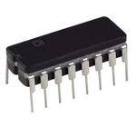
AD624 OUTLINE DIMENSIONS Dimensions shown in inches and (mm). Side-Brazed Solder Lid Ceramic DIP (D-16) 0.005 (0.13) MIN 0.080 (2.03) MAX 16 9 0.310 (7.87) 0.220 (5.59) 1 8 0.320 (8.13) PIN 1 0.290 (7.37) 0.840 (21.34) MAX 0.060 (1.52) 0.015 (0.38) 0.200 (5.08) MAX 0.150 0.200 (5.08) (3.81) 0.125 (3.18) MAX 0.023 (0.58) 0.100 0.070 (1.78)SEATING 0.015 (0.38) 0.014 (0.36) (2.54) 0.030 (0.76)PLANE 0.008 (0.20) BSC REV. C –15–
9 9 7/ – 0 – d 5 0 8 C A. S. U. N D I E T N RI P –16–