ICGOO在线商城 > 集成电路(IC) > 线性 - 放大器 - 仪表,运算放大器,缓冲器放大器 > OPA843IDBVT
 Datasheet下载
- 型号: OPA843IDBVT
- 制造商: Texas Instruments
- 库位|库存: xxxx|xxxx
- 要求:
| 数量阶梯 | 香港交货 | 国内含税 |
| +xxxx | $xxxx | ¥xxxx |
查看当月历史价格
查看今年历史价格
OPA843IDBVT产品简介:
ICGOO电子元器件商城为您提供OPA843IDBVT由Texas Instruments设计生产,在icgoo商城现货销售,并且可以通过原厂、代理商等渠道进行代购。 OPA843IDBVT价格参考¥15.60-¥31.83。Texas InstrumentsOPA843IDBVT封装/规格:线性 - 放大器 - 仪表,运算放大器,缓冲器放大器, 电压反馈 放大器 1 电路 SOT-23-5。您可以下载OPA843IDBVT参考资料、Datasheet数据手册功能说明书,资料中有OPA843IDBVT 详细功能的应用电路图电压和使用方法及教程。
OPA843IDBVT 是 Texas Instruments(德州仪器)推出的一款高性能、低噪声、宽带宽的运算放大器,属于线性放大器系列中的仪表、运算放大器和缓冲器放大器类别。以下是该型号的一些典型应用场景:

 1. 高速信号处理
   - OPA843IDBVT 具有高达 2.5 GHz 的增益带宽积和快速的压摆率(2500 V/µs),非常适合用于高速信号处理系统,例如高速数据采集、射频前端信号调理以及通信系统的信号放大。

 2. 精密测量与传感器信号放大
   - 由于其低噪声特性(电压噪声密度仅为 1.7 nV/√Hz),OPA843IDBVT 可以在高精度测量设备中使用,如医疗成像设备、工业自动化传感器信号放大以及音频信号处理等场景。

 3. 光通信模块
   - 在光通信领域,OPA843IDBVT 被广泛应用于光电探测器的信号放大。其高带宽和低失真性能使其成为驱动模数转换器(ADC)的理想选择,适用于光纤收发器和激光驱动电路。

 4. 视频信号处理
   - OPA843IDBVT 的宽带宽和低失真特性使其适合用于高清视频信号的放大和传输,例如视频监控系统、专业摄像机和显示器接口中的信号链路。

 5. 测试与测量设备
   - 在示波器、频谱分析仪和其他测试设备中,OPA843IDBVT 可作为前端放大器,用于捕捉和放大高频信号,同时保持信号的完整性。

 6. 雷达与国防应用
   - 高速、低噪声的特性使 OPA843IDBVT 成为雷达接收机和国防电子系统中信号放大的理想选择,能够有效处理复杂的高频信号。

 7. 医疗设备
   - 在超声成像、心电图(ECG)和脑电图(EEG)等医疗设备中,OPA843IDBVT 可用于放大微弱的生物电信号,确保信号的质量和精度。

 总结
OPA843IDBVT 凭借其卓越的性能参数(如高带宽、低噪声和快速压摆率),适用于需要高速、高精度信号处理的各种场景,包括通信、医疗、工业自动化和消费电子等领域。
| 参数 | 数值 |
| -3db带宽 | 500MHz |
| 产品目录 | 集成电路 (IC)半导体 |
| 描述 | IC OPAMP VFB 800MHZ SOT23-5高速运算放大器 Wideband Lo-Distort Med Gain Vltg Feedbk |
| 产品分类 | Linear - Amplifiers - Instrumentation, OP Amps, Buffer Amps集成电路 - IC |
| 品牌 | Texas Instruments |
| 产品手册 | http://www.ti.com/litv/sbos268c |
| 产品图片 |
|
| rohs | 符合RoHS无铅 / 符合限制有害物质指令(RoHS)规范要求 |
| 产品系列 | 放大器 IC,高速运算放大器,Texas Instruments OPA843IDBVT- |
| 数据手册 | |
| 产品型号 | OPA843IDBVT |
| 产品 | Voltage Feedback Amplifier |
| 产品种类 | |
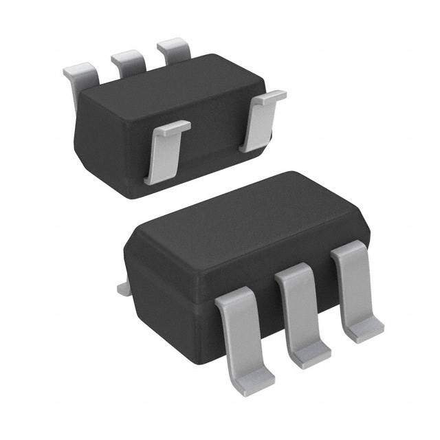
| 供应商器件封装 | SOT-23-5 |
| 共模抑制比—最小值 | 85 dB |
| 其它名称 | 296-14178-1 |
| 包装 | 剪切带 (CT) |
| 单位重量 | 17.500 mg |
| 压摆率 | 1000 V/µs |
| 商标 | Texas Instruments |
| 增益带宽生成 | 800 MHz |
| 增益带宽积 | 800MHz |
| 安装类型 | 表面贴装 |
| 安装风格 | SMD/SMT |
| 封装 | Reel |
| 封装/外壳 | SC-74A,SOT-753 |
| 封装/箱体 | SOT-23-5 |
| 工作温度 | -40°C ~ 85°C |
| 工作电源电压 | 12 V |
| 工厂包装数量 | 250 |
| 拓扑结构 | Voltage Feedback |
| 放大器类型 | 电压反馈 |
| 最大工作温度 | + 85 C |
| 最小工作温度 | - 40 C |
| 标准包装 | 1 |
| 电压-电源,单/双 (±) | 8 V ~ 12 V, ±4 V ~ 6 V |
| 电压-输入失调 | 300µV |
| 电压增益dB | 110 dB |
| 电流-电源 | 20.2mA |
| 电流-输入偏置 | 20µA |
| 电流-输出/通道 | 100mA |
| 电源电流 | 20.8 mA |
| 电路数 | 1 |
| 稳定时间 | 7.5 ns |
| 系列 | OPA843 |
| 设计资源 | http://www.digikey.com/product-highlights/cn/zh/texas-instruments-webench-design-center/3176 |
| 转换速度 | 1000 V/us |
| 输入补偿电压 | 1.2 mV |
| 输出电流 | 100 mA |
| 输出类型 | - |
| 通道数量 | 1 Channel |
| 配用 | /product-detail/zh/DEM-OPA-SOT-1A/296-20840-ND/1216445 |


- 商务部:美国ITC正式对集成电路等产品启动337调查
- 曝三星4nm工艺存在良率问题 高通将骁龙8 Gen1或转产台积电
- 太阳诱电将投资9.5亿元在常州建新厂生产MLCC 预计2023年完工
- 英特尔发布欧洲新工厂建设计划 深化IDM 2.0 战略
- 台积电先进制程称霸业界 有大客户加持明年业绩稳了
- 达到5530亿美元!SIA预计今年全球半导体销售额将创下新高
- 英特尔拟将自动驾驶子公司Mobileye上市 估值或超500亿美元
- 三星加码芯片和SET,合并消费电子和移动部门,撤换高东真等 CEO
- 三星电子宣布重大人事变动 还合并消费电子和移动部门
- 海关总署:前11个月进口集成电路产品价值2.52万亿元 增长14.8%


PDF Datasheet 数据手册内容提取
OPA843 OPA843 www.ti.com SBOS268C – DECEMBER 2002 – DECEMBER 2008 Wideband, Low Distortion, Medium Gain, Voltage-Feedback OPERATIONAL AMPLIFIER FEATURES DESCRIPTION (cid:1) HIGH BANDWIDTH: 260MHz (G = +5) The OPA843 provides a level of speed and dynamic range previously unattainable in a monolithic op amp. Using a high (cid:1) GAIN BANDWIDTH PRODUCT: 800MHz Gain Bandwidth (GBW), two gain-stage design, the OPA843 (cid:1) LOW INPUT VOLTAGE NOISE: 2.0nV/√Hz gives a medium gain range device with exceptional dynamic (cid:1) VERY LOW DISTORTION: –96dBc (5MHz) range. The “classic” differential input complements this high (cid:1) HIGH OPEN-LOOP GAIN: 110dB dynamic range with DC precision beyond most high-speed amplifier products. Very low input offset voltage and current, (cid:1) FAST 12-BIT SETTLING: 10.5ns (0.01%) high Common-Mode Rejection Ratio (CMRR) and Power- (cid:1) LOW INPUT OFFSET VOLTAGE: 300µV Supply Rejection Ratio (PSRR), and high open-loop gain (cid:1) OUTPUT CURRENT: ±100mA combine to give a high DC precision amplifier along with low noise and high 3rd-order intercept. APPLICATIONS 12- to 16-bit converter interfaces will benefit from this combi- nation of features. High-speed transimpedance applications (cid:1) ADC/DAC BUFFER AMPLIFIER can be implemented with exceptional DC precision as well. (cid:1) LOW DISTORTION “IF” AMPLIFIER Differential configurations using two OPA843s can deliver very low distortion to high output voltages, as shown below. (cid:1) ACTIVE FILTERS (cid:1) LOW-NOISE RECEIVER OPA843 RELATED PRODUCTS (cid:1) WIDEBAND TRANSIMPEDANCE INPUT NOISE GAIN-BANDWIDTH (cid:1) TEST INSTRUMENTATION SINGLES VOLTAGE (nV/√Hz) PRODUCT (MHz) (cid:1) PROFESSIONAL AUDIO OPA842 2.6 200 OPA846 1.2 1750 (cid:1) OPA643 UPGRADE OPA847 0.85 3900 +5V DIFFERENTIAL DISTORTION vs OUTPUT VOLTAGE OPA843 –85 G = 10 D R = 400Ω L –5V c) –90 F = 5MHz 40.2Ω 402Ω dB V 1:1 n ( 50IΩ 132Ω40.2Ω 402Ω R40L0Ω VO = 10VI stortio –95 2nd-Harmonic Di c –100 oni 3rd-Harmonic +5V m ar H –105 OPA843 –110 1 10 –5V Output Voltage Swing (Vp-p) Very Low Distortion Differential Driver Please be aware that an important notice concerning availability, standard warranty, and use in critical applications of Texas Instruments semiconductor products and disclaimers thereto appears at the end of this data sheet. All trademarks are the property of their respective owners. PRODUCTION DATA information is current as of publication date. Copyright © 2002-2008, Texas Instruments Incorporated Products conform to specifications per the terms of Texas Instruments standard warranty. Production processing does not necessarily include testing of all parameters. www.ti.com
ABSOLUTE MAXIMUM RATINGS(1) ELECTROSTATIC Power Supply...............................................................................±6.5VDC DISCHARGE SENSITIVITY Internal Power Dissipation......................................See Thermal Analysis Differential Input Voltage..................................................................±1.2V Input Voltage Range............................................................................±V This integrated circuit can be damaged by ESD. Texas Instru- S Storage Voltage Range: D, DBV...................................–65°C to +125°C ments recommends that all integrated circuits be handled with Lead Temperature (soldering, 10s)...............................................+300°C appropriate precautions. Failure to observe proper handling Junction Temperature (TJ)............................................................+150°C and installation procedures can cause damage. ESD Rating (Human Body Model)..................................................2000V (Charge Device Model)...............................................1500V ESD damage can range from subtle performance degrada- (Machine Model)...........................................................200V tion to complete device failure. Precision integrated circuits may be more susceptible to damage because very small NOTE: (1) Stresses above these ratings may cause permanent damage. Exposure to absolute maximum conditions for extended periods may degrade parametric changes could cause the device not to meet its device reliability. These are stress ratings only, and functional operation of the published specifications. device at these or any other conditions beyond those specified is not implied. PACKAGE/ORDERING INFORMATION(1) SPECIFIED PACKAGE TEMPERATURE PACKAGE ORDERING TRANSPORT PRODUCT PACKAGE-LEAD DESIGNATOR RANGE MARKING NUMBER MEDIA, QUANTITY OPA843 SO-8 D –40°C to +85°C OPA843 OPA843ID Rails, 100 " " " " " OPA843IDR Tape and Reel, 2500 OPA843 SOT23-5 DBV –40°C to +85°C OARI OPA843IDBVT Tape and Reel, 250 " " " " " OPA843IDBVR Tape and Reel, 3000 NOTE: (1) For the most current package and ordering information, see the Package Option Addendum at the end of this document, or see the TI website at www.ti.com. PIN CONFIGURATIONS Top View SO Top View SOT Output 1 5 +V S –VS 2 Noninverting Input 3 4 Inverting Input NC 1 8 NC Inverting Input 2 7 +V S Noninverting Input 3 6 Output –V 4 5 NC S 5 4 NC = No Connection OARI 1 2 3 Pin Orientation/Package Marking OPA843 2 www.ti.com SBOS268C
± ELECTRICAL CHARACTERISTICS: V = 5V S ° Boldface limits are tested at +25 C. At T = +25°C, V = ±5V, R = 402Ω, R = 100Ω, and G = +5, unless otherwise noted. See Figure 1 for AC performance. A S F L OPA843ID, OPA843IDBV TYP MIN/MAX OVER TEMPERATURE 0°C to –40°C to MIN/ TEST PARAMETER CONDITIONS +25°C +25°C(1) 70°C +85°C(2) UNITS MAX LEVEL(3 ) AC PERFORMANCE (see Figure 1) Small-Signal Bandwidth (V = 200mV ) G = +3 500 MHz typ C O PP G = +5 260 185 180 175 MHz min B G = +10 85 66 65 64 MHz min B G = +20 40 30 30 30 MHz min B Gain-Bandwidth Product 800 562 560 558 MHz min B Bandwidth for 0.1dB Gain Flatness G = +5, R = 100Ω, V = 200mV 65 34 33 32 MHz min B L O PP Peaking at a Gain of +3 3.5 dB typ C Harmonic Distortion G = +5, f = 5MHz, V = 2V O PP 2nd-Harmonic R = 100Ω –76 –74 –72 –70 dBc max B L R = 500Ω –96 –94 –92 –90 dBc max B L 3rd-Harmonic R = 100Ω –102 –100 –98 –95 dBc max B L R = 500Ω –110 –105 –102 –100 dBc max B L 2-Tone, 3rd-Order Intercept G = +5, f = 25MHz 40 dBm typ C Input Voltage Noise f > 1MHz 2.0 2.2 2.31 2.36 nV/√Hz max B Input Current Noise f > 1MHz 2.8 3.35 3.4 3.45 pA/√Hz max B Rise-and-Fall Time 0.2V Step 1.2 1.95 2.0 2.1 ns max B Slew Rate 2V Step 1000 650 600 525 V/µs min B Settling Time to 0.01% 2V Step 10.5 ns typ C 0.1% 2V Step 7.5 10 10.3 10.6 ns max B 1.0% 2V Step 3.2 5.4 5.8 6.4 ns max B Differential Gain G = +4, NTSC, R = 150Ω 0.001 % typ C L Differential Phase G = +4, NTSC, R = 150Ω 0.012 deg typ C L DC PERFORMANCE(4) Open-Loop Voltage Gain (A ) V = 0V 110 100 96 92 dB min A OL O Input Offset Voltage V = 0V ±0.30 ±1.20 ±1.4 ±1.5 mV max A CM Average Offset Voltage Drift V = 0V ±4 ±4 µV/°C max B CM Input Bias Current V = 0V –20 –35 –36 –37 µA max A CM Input Bias Current Drift V = 0V 25 25 nA/°C max B CM Input Offset Current V = 0V ±0.25 ±1.0 ±1.15 ±1.17 µA max A CM Input Offset Current Drift V = 0V ±2 ±2 nA/°C max B CM INPUT Common-Mode Input Range (CMIR)(5) ±3.2 ±3.0 ±2.9 ±2.8 V min A Common-Mode Rejection (CMRR) V = ±1V, Input Referred 95 85 84 82 dB min A CM Input Impedance Differential-Mode V = 0V 12 || 1 kΩ || pF typ C CM Common-Mode V = 0V 3.2 || 1.2 MΩ || pF typ C CM OUTPUT Output Voltage Swing R > 1kΩ, Positive Output 3.2 3.0 2.9 2.8 V min A L R > 1kΩ, Negative Output –3.7 –3.5 –3.4 –3.3 V min A L R = 100Ω, Positive Output 3.0 2.8 2.7 2.6 V min A L R = 100Ω, Negative Output –3.5 –3.3 –3.2 –3.1 V min A L Current Output V = 0V ±100 ±90 ±85 ±80 mA min A O Closed-Loop Output Impedance G = +5, f = 1kHz 0.0001 Ω typ C POWER SUPPLY Specified Operating Voltage ±5 V typ C Maximum Operating Voltage ±6 ±6 ±6 V max A Minimum Operating Voltage ±4 ±4 ±4 V min A Max Quiescent Current V = ±5V 20.2 20.8 22.2 22.5 mA max A S Min Quiescent Current V = ±5V 20.2 19.6 19.1 18.3 mA min A S Power-Supply Rejection Ratio (+PSRR, –PSRR) |V | = 4.5V to 5.5V, Input Referred 100 90 88 85 dB min A S THERMAL CHARACTERISTICS Specified Operating Range: D, DBV –40 to +85 °C typ C Thermal Resistance, θ Junction-to-Ambient JA D SO-8 125 °C typ C DBV SOT23-5 150 °C typ C NOTES: (1) Junction temperature = ambient temperature for 25°C min/max specifications. (2) Junction temperature = ambient at low temperature limit: junction temperature = ambient +23°C at high temperature limit for over temperature min/max specifications. (3)Test Levels: (A) 100% tested at 25°C over-temperature limits by characterization and simulation. (B) Limits set by characterization and simulation. (C) Typical value only for information. (4) Current is considered positive out- of-node. V is the input common-mode voltage. (5) Tested < 3dB below minimum specified CMRR at ±CMIR limits. CM OPA843 3 SBOS268C www.ti.com
± TYPICAL CHARACTERISTICS: V = 5V S T = +25°C, G = +5, R = 402Ω, R = 100Ω, and R = 100Ω, unless otherwise noted. A F G L NONINVERTING SMALL-SIGNAL INVERTING SMALL-SIGNAL FREQUENCY RESPONSE FREQUENCY RESPONSE 6 3 V = 0.2Vp-p G = +3 G = –8 G = –4 O 3 0 G = +5 n (dB) –03 n (dB) –3 RVGO = = R 0S.2 =V 5p0-pΩ Gai G = +10 Gai –6 d –6 d e e maliz –9 G = +20 maliz –9 G = –16 or or –12 N–12 N G = –32 –15 –15 See Figure 1 See Figure 2 –18 –18 106 107 108 109 106 107 108 109 Frequency (Hz) Frequency (Hz) NONINVERTING LARGE-SIGNAL INVERTING LARGE-SIGNAL FREQUENCY RESPONSE FREQUENCY RESPONSE 17 21 R = 100Ω 0.2Vp-p L G = +5V/V 18 1Vp-p 14 200mVp-p 15 RGL = = – 180V0/ΩV 2Vp-p to 1Vp-p 11 12 Gain (dB) 8 5Vp-p 2Vp-p Gain (dB) 96 5Vp-p 5 3 0 2 –3 See Figure 1 See Figure 2 –1 –6 107 108 109 107 108 109 Frequency (Hz) Frequency (Hz) NONINVERTING PULSE RESPONSE INVERTING PULSE RESPONSE G = +5 Large Signal ± 1V G = –8 Large Signal ± 1V 1.2 1.2 v) v) v) v) V/di 200 Right Scale 0.8 V/di V/di 200 Right Scale 0.8 V/di m m m m 0 100 0.4 0 0 100 0.4 0 0 0 0 0 1 4 1 4 e ( 0 0 e ( e ( 0 0 e ( ag Small Signal ± 100mV ag ag Small Signal ± 100mV ag ut Volt –100 Left Scale –0.4 ut Volt ut Volt –100 Left Scale –0.4 ut Volt p –200 –0.8 p p –200 –0.8 p ut ut ut ut O O O O –1.2 –1.2 See Figure 1 See Figure 2 Time (2ns/div) Time (2ns/div) OPA843 4 www.ti.com SBOS268C
± TYPICAL CHARACTERISTICS: V = 5V (Cont.) S T = +25°C, G = +5, R = 402Ω, R = 100Ω, and R = 100Ω, unless otherwise noted. A F G L 5MHz HARMONIC DISTORTION vs LOAD RESISTANCE 1MHz HARMONIC DISTORTION vs LOAD RESISTANCE –75 –75 VO = 2Vp-p VO = 5Vp-p –80 G = +5 –80 G = +5 c) c) B B d –85 d –85 n ( 2nd-Harmonic n ( o o storti –90 storti –90 2nd-Harmonic c Di –95 c Di –95 ni ni o o m –100 m –100 ar ar 3rd-Harmonic H 3rd-Harmonic H –105 –105 See Figure 1 See Figure 1 –110 –110 100 150 200 250 300 350 400 450 500 100 150 200 250 300 350 400 450 500 Resistance (Ω) Resistance (Ω) HARMONIC DISTORTION vs FREQUENCY HARMONIC DISTORTION vs OUTPUT VOLTAGE –60 –70 VO = 2Vp-p RL = 200Ω G = +5 –75 F = 5MHz Bc) –70 RL = 200Ω Bc) –80 G = +5 d d ortion ( –80 2nd-Harmonic ortion ( –85 2nd-Harmonic Dist Dist –90 nic –90 nic –95 o o 3rd-Harmonic m m ar ar –100 H –100 H 3rd-Harmonic –105 See Figure 1 See Figure 1 –110 –110 0.1 1 10 100 0.1 1 10 Frequency (MHz) Output Voltage Swing (Vp-p) HARMONIC DISTORTION vs NONINVERTING GAIN HARMONIC DISTORTION vs INVERTING GAIN –70 –75 2nd-Harmonic 2nd-Harmonic Bc) –80 Bc) –85 d d V = 2Vp-p Distortion ( –90 VROL == 220V0pΩ-p Distortion ( –95 RFR OLG= = =5 2M500H0ΩzΩ, RF Adjusted nic F = 5MHz nic armo –100 RF = 402Ω, RG Adjusted armo –105 H H 3rd-Harmonic 3rd-Harmonic See Figure 1 See Figure 2 –110 –115 5 10 15 20 5 10 15 20 25 30 35 40 Gain (V/V) Gain (–V/V) OPA843 5 SBOS268C www.ti.com
± TYPICAL CHARACTERISTICS: V = 5V (Cont.) S T = +25°C, G = +5, R = 402Ω, R = 100Ω, and R = 100Ω, unless otherwise noted. A F G L 2-TONE, 3RD-ORDER INPUT VOLTAGE AND CURRENT NOISE DENSITY INTERMODULATION INTERCEPT 10 55 G = +5 PI 50Ω PO 50 50Ω OPA843 √V/Hz√A/Hz +dBm) 45 402Ω 50Ω Voltage Noise nCurrent Noise p CurrVeonltt aNgoei sNeoise2.8p2A./0√nHVz/√Hz ntercept Point ( 4305 100Ω I 30 1 25 102 103 104 105 106 107 10 15 20 25 30 35 40 45 50 55 60 65 70 Frequency (Hz) Frequency (MHz) NONINVERTING GAIN FLATNESS TUNE LOW GAIN INVERTING BANDWIDTH 0.40 3 v) VO = 200mVp-p VO = 200mVp-p di 0.30 A = +4 2 dB Gain (0.1dB/ 00..21000 ESxeVtee rFniaglu Creo 1m0pensation NNGG == 4 4.5 Gain (1dB/div) –110 G = –1 m 12 –0.10 zed –2 G = –2 on fro –0.20 NG = 5 ormali ––34 eviati –0.30 NG = 5.5 N –5 External Compensation G = –3 D See Figure 11 –0.40 –6 1 10 100 1k 1 10 100 1k Frequency (MHz) Frequency (MHz) RECOMMENDED R vs CAPACITIVE LOAD FREQUENCY RESPONSE vs CAPACITIVE LOAD S 100 G = +5 dB) 17 RS adjusted to cap load. d ( a o 14 e L C = 100pF C = 10pF v citi a 11 Ω) ap C = 22pF R (S 10 d Gain to C 8 5V0IΩ OP4A0824Ω3 RS CL 1VkΩO C = 47pF e z 5 ali 100Ω m 1kΩ is optional. or 1 N 2 1 10 100 1k 106 107 108 109 Capacitive Load (pF) Frequency (Hz) OPA843 6 www.ti.com SBOS268C
± TYPICAL CHARACTERISTICS: V = 5V (Cont.) S T = +25°C, G = +5, R = 402Ω, R = 100Ω, and R = 100Ω, unless otherwise noted. A F G L CMRR AND PSRR vs FREQUENCY OPEN-LOOP GAIN AND PHASE 120 120 0 +PSRR Mode Rejection Ratio (dB)pply Rejection Ratio (dB) 108640000 CMRR –PSRR en-Loop Gain (dB) 108640000 20log (AOL) ∠AOL ––––369100020°en-Loop Phase () n-Su Op 20 –150 Op mmower- 20 0 –180 CoPo 0 –20 –210 101 102 103 104 105 106 107 108 101 102 103 104 105 106 107 108 109 Frequency (Hz) Frequency (Hz) CLOSED-LOOP OUTPUT IMPEDANCE OUTPUT VOLTAGE AND CURRENT LIMITATIONS vs FREQUENCY 4 10 3 1 R = 100 OPA843 2 L Ω) ZO 1W Internal e ( 0.1 1 Power Limit nc 402Ω V (V)O –01 RL = 2R5L = 50 put Impeda 00.0.0011 100Ω –2 1W Internal Out Power Limit 0.0001 –3 –4 0.00001 –0.15 –0.1 –0.05 0 0.05 0.1 0.15 102 103 104 105 106 107 108 I (mA) Frequency (Hz) O NONINVERTING OVERDRIVE RECOVERY INVERTING OVERDRIVE RECOVERY 5 1 5 1 4 RigIhntp Suctale RL = G10 =0 Ω5 0.8 4 RLG = = 1 –080Ω 0.8 V/div) 32 LeOftu Stpcuatle See Figure 1 00..64 mV/div) V/div) 32 RigIhntp Suctale See Figure 2 00..64 mV/div) utput Voltage (1 ––1012 00––.002..24 ut Voltage (200 utput Voltage (1 ––1012 LeOftu Stpcuatle 00––.002..24 ut Voltage (200 O p O p –3 –0.6 n –3 –0.6 n I I –4 –0.8 –4 –0.8 –5 –1 –5 –1 Time (40ns/div) Time (40ns/div) OPA843 7 SBOS268C www.ti.com
± TYPICAL CHARACTERISTICS: V = 5V (Cont.) S T = +25°C, G = +5, R = 402Ω, R = 100Ω, and R = 100Ω, unless otherwise noted. A F G L SETTLING TIME VIDEO DIFFERENTIAL GAIN/DIFFERENTIAL PHASE 0.25 R = 100Ω 0.02 0.1 0.20 V =L 2V step G = +4 dG, Negative Video O %) 0.15 G = +5 of Final Value ( –000...1000505 ential Gain (%) 0.00.1051 dP, Negative Video dP, Positive Video 00..00755 °ential Phase () Percent ––00..1105 Differ 0.005 0.025 Differ dG, Positive Video –0.20 See Figure 1 –0.25 0 0 0 5 10 15 20 25 1 2 3 4 5 Time (ns) Video Loads (150Ω each) TYPICAL DC DRIFT OVER TEMPERATURE SUPPLY AND OUTPUT CURRENT vs TEMPERATURE 1 25 110 22 A) µ ge (mV) 0.5 VIO 12.5 Current ( mA/div) 106 Supply Current 21 mA/div) Input Offset Volta –0.50 100 x IOSI 0–12.5 ut Bias and Offset Output Current (2 1099842 SSoinukrciningg O Ouutptpuut tC Cuurrrerenntt 211098 Supply Current (1 B p n I –1 –25 90 17 –50 –25 0 25 50 75 100 125 –50 –25 0 25 50 75 100 125 Ambient Temperature (°C) Ambient Temperature (°C) COMMON-MODE INPUT RANGE AND OUTPUT SWING COMMON-MODE AND DIFFERENTIAL vs SUPPLY VOLTAGE INPUT IMPEDANCE 6 107 Positive Input Ω)) Common-Mode 4 g ( 106 o ge (V) 2 de (20l 105 n Positive Output u Ra 0 nit e ag Differential g M 104 Volta –2 Negative Output nce a –4 ped 103 Negative Input m I –6 102 3 4 5 6 103 104 105 106 107 108 Supply Voltage (±V) Frequency (Hz) OPA843 8 www.ti.com SBOS268C
± TYPICAL CHARACTERISTICS: V = 5V (Cont.) S T = +25°C, G = 10, R = 1kΩ, R = 100Ω, and R = 100Ω, unless otherwise noted. A D F G L DIFFERENTIAL PERFORMANCE DIFFERENTIAL SMALL-SIGNAL TEST CIRCUIT FREQUENCY RESPONSE 3 +5V V = 400mVp-p O G = 5 D 0 1R00GΩ OP–AR584VF3 GD = 10R0FΩ d Gain (dB) ––36 GD = 32 GGDD == 1106 e z –9 VI 1R00GΩ RF RL VO ormali –12 N +5V –15 OPA843 –18 1 10 100 1k –5V Frequency (MHz) DIFFERENTIAL LARGE-SIGNAL FREQUENCY RESPONSE DIFFERENTIAL DISTORTION vs LOAD RESISTANCE 23 –70 V = 4Vp-p GD = 10V/V VO = 400mVp-p to 5Vp-p –75 GO = 10 D 20 c) F = 5MHz B –80 d on ( –85 dB) 17 orti 2nd-Harmonic Gain ( 14 VO = 8Vp-p nic Dist ––9905 o m ar –100 11 H 3rd-Harmonic –105 8 –110 10 100 200 10 100 1k Frequency (MHz) Load Resistance (Ω) DIFFERENTIAL DISTORTION vs FREQUENCY DIFFERENTIAL DISTORTION vs OUTPUT VOLTAGE –60 –80 VO = 4Vp-p GD = 10 GD = 10 –85 RL = 400Ω –70 RL = 400Ω Bc) F = 5MHz d –90 n ( dB) –80 ortio –95 Gain ( –90 2nd-Harmonic c Dist –100 2nd-Harmonic oni 3rd-Harmonic m –105 ar –100 H 3rd-Harmonic –110 –110 –115 1 10 20 1 10 Frequency (Hz) Output Voltage Swing (Vp-p) OPA843 9 SBOS268C www.ti.com
APPLICATIONS INFORMATION +5V WIDEBAND NONINVERTING OPERATION The OPA843’s combination of speed and dynamic range is useful in a wide variety of application circuits, as long as 0.1µF + 2.2µF simple guidelines common to all high-speed amplifiers are observed. For example, good power-supply decoupling, as R 50Ω Load S shown in Figure 1, is essential to achieve the lowest possible V 50Ω RT OPA843 O harmonic distortion and smooth frequency response. Careful PC board layout and component selection will maximize the performance of the OPA843 in all applications, as discussed 50Ω Source RG RF 50Ω 402Ω in the following sections of this data sheet. Figure 1 shows V I the gain of +5 configuration used as the basis for most of the Typical Characteristics. Most of the curves were character- R M ized using signal sources with 50Ω driving impedance and (optional) 0.1µF 2.2µF with measurement equipment presenting 50Ω load imped- + ance. In Figure 1, the 50Ω shunt resistor at the input terminal matches the source impedance of the test generator, while –5V the 50Ω series resistor at the V terminal provides a match- O ing resistor for the measurement equipment load. Generally, FIGURE 2. Inverting G = –8 Specification and Test Circuit. data sheet specifications refer to the voltage swing at the output pin (V in Figure 1) while those referring to load power both the input termination resistor and the gain setting O are at the 50Ω load. The total 100Ω load from the series and resistor for the circuit. Although the signal gain for the circuit shunt matching resistors, combined with the 502Ω total of Figure 2 is equal to –8V/V (versus the +5V/V for Figure 1), feedback network load, presents the OPA843 with an effec- their noise gains are equal when the 50Ω source resistor is tive output load of approximately 83Ω. included. This has the interesting effect of nearly doubling the equivalent Gain Bandwidth Product (GBP) for the ampli- fier. This can be seen in comparing the G = +5 and G = –8 +5V small-signal frequency response curves. Both show approxi- +V S mately 260MHz bandwidth, but the inverting configuration of Figure 2 is giving 4dB higher signal gain. If the signal source + is actually the low impedance output of another amplifier, R 0.1µF 2.2µF G 50Ω Source is increased to the minimum value allowed at the output of RS 50Ω Load that amplifier and RF is adjusted to get the desired gain. It is VIN 50Ω OPA843 VO 50Ω carmitipclaifli efro sr hsotawb ale v eorpye lroawtio onu topfu tt hime pOePdaAn8c4e3 ththroaut gthhi sfr edqriuveinng- cies exceeding the expected closed-loop bandwidth for the R OPA843. F 402Ω An optional input termination resistor is also shown in Figure 2. This R resistor may be used to adjust the input impedance to M R10G0Ω lower values when RG needs to be adjusted higher. This might 0.1µF +2.2µF be desirable at lower gains where increasing RF will reduce the output loading improving harmonic distortion performance. For instance, at a gain of –4 an R set to 50Ω will require a 200Ω –V G –5V S feedback resistor. In this case, adjusting RF to 400Ω, setting RG to 100Ω, and then adding a 100Ω R resistor will deliver a gain M FIGURE 1. Gain of +5, High-Frequency Application and of –4 with a 50Ω input match. Characterization Circuit. BUFFERING HIGH-PERFORMANCE ADCs WIDEBAND, INVERTING GAIN OPERATION A single-channel interface using the OPA843 can provide a low There can be significant benefits to operating the OPA843 as noise/distortion interface to emerging 14-bit Analog-to-Digital an inverting amplifier. This is particularly true when a matched Converters (ADCs) through approximately 5MHz for medium input impedance is required. Figure 2 shows the inverting gain applications. Since the dominant distortion mechanism is gain circuit used as a starting point for the typical character- 2nd-harmonic distortion, differential circuits using the OPA843 istics showing inverting mode performance. can extend this frequency range and/or power level to much Driving this circuit from a 50Ω source, and constraining the higher levels. The example on the front page of this data sheet, gain resistor, R , to equal 50Ω will give both a signal for instance, shows better than 93dB SFDR at 5MHz for up to G 8V signals. This is still being limited by the 2nd-harmonic with bandwidth and noise advantage. R in this case is acting as PP G OPA843 10 www.ti.com SBOS268C
the 3rd-harmonic much lower. 2-tone 3rd-order intermodulation 1dB through 50MHz. For narrowband IF’s in the 44MHz terms will be much lower than most other solutions using the region, this configuration of the OPA843 will show a 3rd-order circuit shown on the front page. The differential typical charac- intercept of 33dBm while dissipating only 200mW (23dBm) teristic curves also show that a 4V output will have power from ±5V supplies. PP > 80dBc SFDR through 20MHz using this differential approach. PHOTODIODE TRANSIMPEDANCE AMPLIFIER WIDE DYNAMIC RANGE “IF” AMPLIFIER High Gain Bandwidth Product (GBP) and low input voltage The OPA843 offers an attractive alternative to standard fixed- and current noise make the OPA843 an ideal wideband gain IF amplifier stages. Narrowband systems will benefit from transimpedance amplifier for low to moderate gains. Note the exceptionally high 2-tone 3rd-order intermodulation inter- that unity-gain stability is not required for transimpedance cept, as shown in the Typical Characteristics. Op amps with applications. Figure 4 shows an example photodiode ampli- high open-loop gain, like the OPA843, provide an intercept fier circuit. The key parameters of this design are the esti- that decreases with frequency along with the loop gain. The mated diode capacitance (C ) at the applied DC reverse bias D OPA843’s 3rd-order intercept shows a decreasing intercept voltage (–V ), the desired transimpedance gain (R ), and the B F with frequency. The OPA843’s intercept is > 30dBm up to GBP for the OPA843 (800MHz). With these three variables 50MHz but improves to > 50dBm as the operating frequency set (and adding the OPA843’s parasitic input capacitance to is reduced below 10MHz. Broadband systems will also benefit the value of C to get C ), the feedback capacitor value (C ) D S F from the very low even-order harmonics and intermodulation is selected to provide stability for the transimpedance fre- components produced by the OPA843. Compared to standard quency response. fixed-gain IF amplifiers, the OPA843 operating at IF’s below 50MHz provides much higher intercepts for its quiescent power dissipation (200mW), superior gain accuracy, higher +5V reverse isolation, and lower I/O return loss. The noise figure Power-supply decoupling for the OPA843 will be higher than alternative fixed-gain not shown. stages. If the application comes late in the amplifier chain with 0.01µF 10kΩ OPA843 V = I R O D F significant gain in prior stages, this higher noise figure may be acceptable. Figure 3 shows an example of a noninverting configuration for the OPA843 used as an IF amplifier. R –5V 10kFΩ λ +5V Power-supply ID C20DpF 0.7C5FpF decoupling not shown. 50Ω Source 0.01µF PI V 5R0SΩ 50Ω Load –VB O 52.3Ω 1kΩ OPA843 P0 FIGURE 3. High Dynamic Range IF Amplifier. R To achieve a maximally flat 2nd-order Butterworth frequency F +5V 1kΩ response, the feedback pole should be set to: C =C +C R14G4Ω 2πR1C = 4πGRBPC S D I (1) F F F S 0.01µF Adding the OPA843’s common-mode and differential mode input capacitances C = (1.0 + 1.2)pF to the 20pF diode I Gain=PPOI =20log 12 1+RRGF dB=12dBwithvaluesshown ssiomuprceed acnacpea cgitaainnc ues oinf gF tighuer e8 040, MaHndz tGarBgPe tifnogr tah e1 0OkPΩA t8ra4n3-, the required feedback pole frequency is 16.9MHz. This will require a total feedback capacitance of 0.94pF. Typical FIGURE 3. High Dynamic Range IF Amplifier. surface-mount resistors have a parasitic capacitance of 0.2pF, leaving the required 0.75pF value shown in Figure 4 The input signal and the gain resistor are AC-coupled through the 0.01µF blocking capacitors. This holds the DC input and to get the required feedback pole. output operating point at ground independent of source im- This will set the –3dB bandwidth according to: pedance and gain setting. The R value in Figure 3 (144Ω), G GBP stoeletsr athnec eg areins itsot othrse fmora Rtch aendd lo Rad watil l1 h2odlBd .t hUes ignagi ns ttaon ad ±a0rd.2 1d%B F−3dB ≅ 2πRFCSHz (2) F G tolerance. This example will give a –3dB bandwidth of ap- The example of Figure 4 will give approximately 24MHz proximately 100MHz while maintaining gain flatness within –3dB bandwidth using the 0.75pF feedback compensation. OPA843 11 SBOS268C www.ti.com
WIDEBAND INVERTING SUMMING AMPLIFIER 100pF One common application for a wideband op amp like the OPA843 is to sum a number of signal sources together. V 61Ω 150Ω 0Ω I Figure 5 shows the inverting summing configuration that is Source most often used. This circuit offers the benefit that each input VO 220pF OPA843 sees an input impedance set only by its individual input resistor, since the summing junction (inverting op amp node) is a virtual ground. Each input is non-interactive with every 402Ω other. However, the bandwidth from any input to the summed output is set by the op amp noise gain (NG), which is equal 100Ω to the noninverting voltage gain. Therefore, each inverting channel may have a low gain to the output (like the –1 shown in Figure 5); this noise gain will set the frequency response and the loop stability. The noninverting gain for Figure 5 is FIGURE 6. 10MHz Butterworth Low-Pass Filter. equal to +5, which will give a 260MHz bandwidth at a gain of –1 for each of the input signals. 10MHz Low-Pass Filter 15 12 +5V 9 Power-supply decoupling not shown. 6 0.1µF 81.8Ω OPA843 VO = –(V1 + V2 + V3 + V4) n (dB) 30 ai G –3 –5V –6 R –9 F 402Ω 402Ω –12 V 1 –15 402Ω 100k 1M 10M 100M V2 Frequency (MHz) 402Ω FIGURE 7. Frequency Response for Figure 6. V 3 402Ω V transition from a unity gain receiver at lower frequencies 4 (through the R path) to a gain of 20dB (10V/V) through the 5 FIGURE 5. Wideband Inverting Summing Amplifier. R1 path at higher frequencies. The component values have been selected to set the peak gain at approximately 30MHz. A unique feature for this circuit is an independent tune on the 2nd-Order Filter Topology width of the peaking (Q of the response) by adjusting R . G High-speed amplifiers like the OPA843 are good choices for See Figure 9 for the effect of adjusting R over the range of G 2nd-order filter building blocks as part of ADC driver chan- 20Ω to 100Ω. nels. These can provide noise bandlimiting to improve the SNR for the amplifier/converter combination. The circuit of DESIGN-IN TOOLS Figure 6 shows an example of a 10MHz Butterworth low- pass filter where the amplifier provides a low frequency gain DEMONSTRATION FIXTURES of 5 and a 2nd-order cutoff at 10MHz. The resistor values Two printed circuit boards (PCBs) are available to assist in have been adjusted slightly to account for the amplifier the initial evaluation of circuit performance using the OPA843 bandwidth. Figure 7 shows the small-signal frequency re- in its two package options. Both of these are offered free of sponse for this filter. charge as unpopulated PCBs, delivered with a user's guide. The summary information for these fixtures is shown in the EQUALIZING FILTER APPLICATION table below. In sensor receiver applications, where the pickup is a sensor or cable giving a bandlimited frequency response, an equal- ORDERING LITERATURE izing filter can sometimes be used to extend the useable PRODUCT PACKAGE NUMBER NUMBER frequency range for the sensor. This is done mathematically OPA843U SO-8 DEM-OPA-SO-1A SBOU009 by taking the inverse of the rolloff transfer function and OPA843N SOT23-5 DEM-OPA-SOT-1A SBOU010 implementing that as the amplifier frequency response. See Figure 8 for one example of a wideband equalizer where two The demonstration fixtures can be requested at the Texas stages of the OPA843 are used. This example is set to Instruments web site (www.ti.com) through the OPA843 product folder. OPA843 12 www.ti.com SBOS268C
+5V +5V V V CC CC OPA843 OPA843 VOUT Power-supply decoupling not shown. R V V LOAD –5V EE –5V EE 1kΩ R4 C2 RF R1 R2 600Ω 41.125pF 1.2kΩ 120Ω 1.2kΩ V IN C 1 5.2pF R G R 5 1.2kΩ FIGURE 8. Adjustable Equalizer. value should be between 200Ω and 1kΩ. Below 200Ω, the 40 feedback network will present additional output loading that can degrade the harmonic distortion performance of the OPA843. Above 1kΩ, the typical parasitic capacitance (ap- 20 proximately 0.2pF) across the feedback resistor may cause unintentional band limiting in the amplifier response. B) 0 (d A good rule of thumb is to target the parallel combination of R and R (see Figure 1) to be less than about 200Ω. The F G –20 combined impedance R || R interacts with the inverting F G input capacitance, placing an additional pole in the feedback network, and thus a zero in the forward response. Assuming –40 100kHz 1MHz 10MHz 100MHz 1GHz a 2pF total parasitic on the inverting node, holding R || R F G Frequency < 200Ω will keep this pole above 400MHz. By itself, this constraint implies that the feedback resistor R can increase FIGURE 9. Equalizer Plot, Multiple Settings. F to several kΩ at high gains. This is acceptable as long as the pole formed by R and any parasitic capacitance appearing F MACROMODELS AND APPLICATIONS SUPPORT in parallel is kept out of the frequency range of interest. Computer simulation of circuit performance using SPICE is In the inverting configuration, an additional design consider- often a quick way to analyze the performance of the OPA843 ation must be noted. R becomes the input resistor and, G and its circuit designs. This is particularly true for video and therefore, the load impedance to the driving source. If imped- RF amplifier circuits where parasitic capacitance and induc- ance matching is desired, R may be set equal to the G tance can play a major role on circuit performance. A SPICE required termination value. However, at low inverting gains model for the OPA843 is available through the TI web page the resultant feedback resistor value can present a signifi- (http://www.ti.com). The applications department is also avail- cant load to the amplifier output. For example, an inverting able for design assistance. These models predict typical gain of –4 with a 50Ω input matching resistor (= R ) would G small-signal AC, transient steps, DC performance, and noise require a 200Ω feedback resistor, which would contribute to under a wide variety of operating conditions. The models output loading in parallel with the external load. In such a include the noise terms found in the electrical specifications case, it would be preferable to increase both the R and R F G of this data sheet. These models do not attempt to distin- values, and then achieve the input matching impedance with guish between the package types in their small-signal AC a third resistor to ground; see Figure 2. The total input performance. impedance becomes the parallel combination of R and the G additional shunt resistor. OPERATING SUGGESTIONS BANDWIDTH vs GAIN OPTIMIZING RESISTOR VALUES Voltage-feedback op amps exhibit decreasing closed-loop Since the OPA843 is a voltage-feedback op amp, a wide bandwidth as the signal gain is increased. In theory, this range of resistor values may be used for the feedback and relationship is described by the GBP shown in the Electrical gain setting resistors. The primary limits on these values are Characteristics. Ideally, dividing GBP by the noninverting set by dynamic range (noise and distortion) and parasitic signal gain (also called the Noise Gain, or NG) will predict the capacitance considerations. Usually, the feedback resistor closed-loop bandwidth. In practice, this only holds true when OPA843 13 SBOS268C www.ti.com
the phase margin approaches 90°, as it does in high-gain tune the flatness by adjusting R. The Typical Characteristics I configurations. At low signal gains, most amplifiers will ex- show a signal gain of +4 with the noise gain adjusted for hibit a more complex response with lower phase margin. The flatness using different values for R . 1 OPA843 is optimized to give a maximally flat 2nd-order Where low gain is desired, and inverting operation is accept- Butterworth response in a gain of 5. In this configuration, the able, a new external compensation technique may be used to OPA843 has approximately 60° of phase margin and will retain the full slew rate and noise benefits of the OPA843 while show a typical –3dB bandwidth of 260MHz. When the phase maintaining the increased loop gain and the associated im- margin is 60°, the closed-loop bandwidth is approximately √2 provement in distortion offered by the decompensated archi- greater than the value predicted by dividing GBP by the noise tecture. This technique shapes the noise gain for good stability gain. Increasing the gain will cause the phase margin to while giving an easily controlled 2nd-order low-pass frequency approach 90° and the bandwidth to more closely approach response. Figure 11 shows this circuit. Considering only the the predicted value of (GBP/NG). At a gain of +20, the noise gain for the circuit of Figure 11, the low-frequency noise 40MHz bandwidth shown in the Electrical Characteristics gain (NG ) will be set by the resistor ratios while the high- 1 agrees with that predicted using the simple formula and the frequency noise gain (NG ) will be set by the capacitor ratios. 2 typical GBP of 800MHz. The capacitor values set both the transition frequencies and the high-frequency noise gain. If this noise gain, determined by LOW GAIN OPERATION NG = 1 + C /C , is set to a value greater than the recom- 2 S F mended minimum stable gain for the op amp and the noise Decreasing the operating gain for the OPA843 from the gain pole (set by 1/R C ) is placed correctly, a very well nominal design point of +5 will decrease the phase margin. F F controlled 2nd-order low-pass frequency response will result. This will increase the Q for the closed-loop poles, peak up the frequency response, and extend the bandwidth. A peaked frequency response will show overshoot and ringing in the pulse response as well as a higher integrated output noise. +5V Operating at a noise gain less than +3 runs the risk of Power-supply decoupling not shown. sustained oscillation (loop instability). However, operation at low gains would be desirable to take advantage of the much 0.1µF 280Ω OPA843 VO higher slew rate and lower input noise voltage available in the OPA843, as compared to the performance offered by unity-gain stable op amps. Numerous external compensation –5V techniques have been suggested for operating a high-gain R F op amp at low gains. Most of these give zero/pole pairs in the 402Ω 806Ω V closed-loop response that cause long term settling tails in the 1 pulse response and/or phase nonlinearity in the frequency RS = 0Ω CS 1.C9pFF response. Figure 10 shows an external compensation method 12.6pF for a noninverting configuration that does not suffer from these drawbacks. FIGURE 10. Noninverting Low Gain Circuit. +5V To choose the values for both C and C , two parameters 50Ω Source S F and only three equations need to be solved. The first param- VI R50TΩ R1313Ω OPA843 VO 5R0SΩ eshteoru lids bthee gtraeragteetr htihgahn-f rtehqeu emnicnyim nuomis es tgaabilne, gNaGin2 , fowr htihche 50Ω Load OPA843. Here, a target NG2 of 7.5 will be used. The second parameter is the desired low-frequency signal gain, which R F also sets the low-frequency noise gain, NG . To simplify this +5V 402Ω 1 discussion, we will target a maximally flat 2nd-order low-pass Butterworth frequency response (Q = 0.707). The signal gain R G 402Ω of –2 shown in Figure 11 will set the low-frequency noise gain to NG = 1 + R /R (= 3 in this example). Then, using only 1 F G these two gains and the GBP for the OPA843 (800MHz), the FIGURE 10. Noninverting Low Gain Circuit. key frequency in the compensation is determined by: GBP NG NG The R1 resistor across the two inputs will increase the noise Z0 = NG12 1−NG21 − 1−2NG21 (11) gain (i.e., decrease the loop gain) without changing the signal gain. This approach will retain the full slew rate to the Physically, this Z (13.6MHz for the values shown in Figure 11) 0 output but will give up some of the low-noise benefit of the is set by 1/(2π • R (C + C )) and is the frequency at which F F S OPA843. Assuming a low source impedance, set R so that the rising portion of the noise gain would intersect unity gain 1 1 + R /(R || R) is ≥ +3. This approach may also be used to if projected back to 0dB gain. The actual zero in the noise gain F G I OPA843 14 www.ti.com SBOS268C
occurs at NG • Z and the pole in the noise gain occurs at susceptible to decreased stability and closed-loop response 1 0 NG • Z . Since GBP is expressed in Hz, multiply Z by 2π and peaking when a capacitive load is placed directly on the 2 0 0 use this to get C by solving: output pin. In simple terms, the capacitive load reacts with F the open-loop output resistance of the amplifier to introduce 1 CF = 2πR Z NG (12) an additional pole into the loop and thereby decrease the F 0 2 phase margin. This issue has become a popular topic of Finally, since C and C set the high-frequency noise gain, application notes and articles, and several external solutions S F determine C by: to this problem have been suggested. When the primary S considerations are frequency-response flatness, pulse re- C = (NG – 1)C (13) S 2 F sponse fidelity, and/or distortion, the simplest and most The resulting closed-loop bandwidth will be approximately effective solution is to isolate the capacitive load from the equal to: feedback loop by inserting a series isolation resistor between f−3dB ≅ Z0GBP (14) the amplifier output and the capacitive load. This does not eliminate the pole from the loop response, but rather shifts it For the values shown in Figure 10, the f will be approxi- –3dB and adds a zero at a higher frequency. The additional zero mately 105MHz. This is less than that predicted by simply acts to cancel the phase lag from the capacitive load pole, dividing the GBP product by NG . The compensation network 1 thus increasing the phase margin and improving stability. controls the bandwidth to a lower value while providing full slew rate and exceptional distortion performance due to in- The Typical Characteristics show the recommended R vs S creased loop gain at frequencies below NG • Z . The capaci- Capacitive Load and the resulting frequency response at the 1 0 tor values shown in Figure 10 are calculated for NG = 3 and load. The criterion for setting the recommended resistor is 1 NG = 7.5 with no adjustment for parasitics. maximum bandwidth and flat frequency response at the load. 2 Since there is now a passive low-pass filter between the OUTPUT DRIVE CAPABILITY output pin and the load capacitance, the response at the output pin itself is typically somewhat peaked, and becomes The OPA843 has been optimized to drive the demanding load flat after the roll off action of the RC network. This is not a of a doubly-terminated transmission line. When a 50Ω line is concern in most applications, but can cause clipping if the driven, a series 50Ω into the cable and a terminating 50Ω load desired signal swing at the load is very close to the amplifier’s at the end of the cable are used. Under these conditions, the swing limit. impedance of the cable appears resistive over a wide fre- Parasitic capacitive loads greater than 2pF can begin to quency range and the total effective load on the OPA843 is 100Ω in parallel with the resistance of the feedback network. degrade the performance of the OPA843. Long PC board traces, unmatched cables, and connections to multiple de- The Electrical Characteristics show a 6.1V swing into a PP 100Ω load—which is then reduced to a 3V swing at the vices can easily cause this value to be exceeded. Always PP termination resistor. The ±85mA output drive over tempera- consider this effect carefully and add the recommended series resistor as close as possible to the OPA843 output pin ture provides adequate current drive margin for this load. (see Board Layout section). A common IF amplifier specification, which describes avail- able output power is the –1dB compression point. This is DISTORTION PERFORMANCE usually defined at a matched 50Ω load to be the sinusoidal power where the gain has compressed by –1dB vs the gain The OPA843 is capable of delivering an exceptionally low seen at very low power levels. This compression level is distortion signal at high frequencies and medium gains. The frequency dependent for an op amp, due to both bandwidth distortion plots in the Typical Characteristics show the typical and slew rate limitations. For frequencies well within the distortion under a wide variety of conditions. Most of these bandwidth and slew rate limit of the OPA843, the –1dB plots are limited to 100dB dynamic range. The OPA843’s compression at a matched 50Ω load will be > 13dBm based distortion does not rise above –100dBc until either the signal on the minimum available 3Vp-p swing at the load. One level exceeds 0.5Vp-p and/or the fundamental frequency common use for the –1dB compression is to predict exceeds 500kHz. intermodulation intercept. This is normally 10dB greater than Distortion in the audio band is < –120dBc. the –1dB compression power for a standard RF amplifier. This Generally, until the fundamental signal reaches very high simple rule of thumb does NOT apply to the OPA843. The high frequencies or powers, the 2nd-harmonic will dominate the open-loop gain and Class AB output stage of the OPA843 distortion with a negligible 3rd-harmonic component. Focus- produce a much higher intercept than the –1dB compression ing then on the 2nd-harmonic, increasing the load imped- would predict, as shown in the Typical Characteristics. ance improves distortion directly. Remember that the total load includes the feedback network—in the noninverting DRIVING CAPACITIVE LOADS configuration this is the sum of R + R , whereas in the F G One of the most demanding, and yet very common, load inverting configuration this is just RF (see Figure 1). Increas- conditions for an op amp is capacitive loading. A high-speed, ing output voltage swing increases harmonic distortion di- high open-loop gain amplifier like the OPA843 can be very rectly. A 6dB increase in output swing will generally increase OPA843 15 SBOS268C www.ti.com
the 2nd-harmonic 12dB and the 3rd-harmonic 18dB. Increas- shows the general form for this output noise voltage using the ing the signal gain will also increase the 2nd-harmonic terms presented in Figure 12. distortion. Again, a 6dB increase in gain will increase the ( ) 2nd- and 3rd-harmonic by 6dB even with a constant output E = E2 +(I R )2+4kTR NG2+(I R )2+4kTR NG (15) O NI BN S S BI F F power and frequency. Finally, the distortion increases as the fundamental frequency increases due to the roll off in the loop gain with frequency. Conversely, the distortion will ENI improve going to lower frequencies down to the dominant open-loop pole at approximately 3kHz. Starting from the RS IBN OPA843 EO –100dBc 2nd-harmonic for 2V into 200Ω, G = +5 distortion PP at 500kHz (from the Typical Characteristics), the 2nd-har- ERS monic distortion at 20kHz should be approximately: √4kTRS RF –100dB – 20log (500kHz/20kHz) = –128dBc. 4kT RG IBI √4kTRF 4kT = 1.6E – 20J The OPA843 has an extremely low 3rd-order harmonic distortion. RG at 290°K This also gives an exceptionally good 2-tone, 3rd-order intermodulation intercept, as shown in the Typical Characteristics. FIGURE 12. Op Amp Noise Analysis Model. This intercept curve is defined at the 50Ω load when driven through a 50Ω-matching resistor to allow direct comparisons to RF MMIC Dividing this expression by the noise gain (NG = 1 + RF/RG) devices. This network attenuates the voltage swing from the output will give the equivalent input referred spot noise voltage at pin to the load by 6dB. If the OPA843 drives directly into the input the noninverting input, as shown in Equation 16. of a high-impedance device, such as an ADC, this 6dB attenuation is not taken. Under these conditions, the intercept will increase by E = E2 +(I R )2 +4kTR +IBIRF2 + 4kTRF (16) a minimum of 6dBm. The intercept is used to predict the N NI BN S S NG NG intermodulation spurious for two closely spaced frequencies. If the Evaluating these two equations for the OPA843 circuit pre- two test frequencies, f and f, are specified in terms of average and 1 2 sented in Figure 1 will give a total output spot noise voltage delta frequency, f = (f + f)/2 and µf = |f – f|/2, the two, 3rd-order, O 1 2 2 1 of 12.4nV/√Hz and an equivalent input spot noise voltage of close-in spurious tones will appear at f ± (3 • ∆f). The difference O 2.48nV/√Hz. between two equal test-tone power levels and these intermodulation spurious power levels is given by 2 • (IM3 – P ) O DC OFFSET CONTROL where IM3 is the intercept taken from the typical characteristic curve and P is the power level in dBm at the 50Ω load for one of The OPA843 can provide excellent DC signal accuracy due to O the two closely spaced test frequencies. For instance, at 10MHz the its high open-loop gain, high common-mode rejection, high OPA843 at a gain of +5 has an intercept of 49dBm at a matched power supply rejection, and low input offset voltage and bias 50Ω load. If the full envelope of the two frequencies needs to be current offset errors. To take full advantage of this low input 2Vp-p, this requires each tone to be 4dBm. The 3rd-order offset voltage, careful attention to input bias current cancella- intermodulation spurious tones will then be 2 • (49 – 4) = 90dBc tion is also required. The high-speed input stage for the below the test-tone power level (–86dBm). If this same 2Vp-p 2- OPA843 has a relatively high input bias current (20µA typical tone envelope were delivered directly into the input of an ADC into the pins) but with a very close match between the two without the matching loss or loading of the 50Ω network, the input currents—typically 0.17µA input offset current. Figures intercept would increase to at least 55dBm. With the same signal 13 and 14 show typical distribution of input offset voltage and and gain conditions now driving directly into a light load, the current for the OPA843. spurious tones will then be at least 2 • (55 – 4) = 102dBc below the 1V test-tone signal levels. PP 1000 Mean = 0.38mV 900 NOISE PERFORMANCE Standard Deviation = 0.31mV 800 Total Count = 5572 The OPA843 complements its ultra low harmonic distortion 700 with low input noise terms. Both the input-referred voltage 600 noise, and the two input-referred current noise terms com- nt u 500 o bine to give a low output noise under a wide variety of C 400 operating conditions. Figure 12 shows the op amp noise 300 analysis model with all the noise terms included. In this 200 model, all the noise terms are taken to be noise voltage or current density terms in either nV/√Hz or pA/√Hz. 100 0 The total output spot noise voltage is computed as the square 0864208642024680246800 2098764321012346789022 root of the squared contributing terms to the output noise 1.1.0.0.0.0.0.0.0.0.0.0.0.0.0.0.0.0.0.1.1.1. –––––––––––<<<<<<<<<<> voltage. This computation is adding all the contributing noise < < < < < < < < < < < mV powers at the output by superposition, and then taking the square root to get back to a spot noise voltage. Equation 15 FIGURE 13. Input Offset Voltage Distributing in mV. OPA843 16 www.ti.com SBOS268C
+5V 1600 Mean = 0.04µA VCC 1400 Standard Deviation = 0.17µA Power-supply decoupling Total Count = 5572 not shown. 1200 OPA843 V 0.1µF 200Ω O 1000 nt Cou 800 VEE –5V 600 +5V R R G F 400 250Ω 1kΩ V 200 5kΩ IN 0 20kΩ ±125mV Output Adjustment 0000000000000000000000 1.00.90.80.70.60.50.40.30.20.10.00.10.20.30.40.50.60.70.81.91.01.0 10kΩ –––––––––––<<<<<<<<<<> < < < < < < < < < < < 0.1µF V R mV O = – F = –4 5kΩ V R IN G FIGURE 14. –5V The total output offset voltage may be considerably reduced FIGURE 15. DC-Coupled, Inverting Gain of –4 with Output by matching the source impedances looking out of the two Offset Adjustment. inputs. For example, one way to add bias current cancellation to the circuit of Figure 1 would be to insert a 55Ω series resistor resistor values for setting this offset adjustment are chosen into the noninverting input from the 50Ω terminating resistor. to be much larger than the signal path resistors. This will When the 50Ω source resistor is DC coupled, this will increase insure that this adjustment has minimal impact on the loop the source impedance for the noninverting input bias current gain and hence, the frequency response. to 80Ω. Since this is now equal to the impedance looking out of the inverting input (R || R ), the circuit will cancel the gains F G for the bias currents to the output leaving only the offset THERMAL ANALYSIS current times the feedback resistor as a residual DC error term The OPA843 will not require heat sinking or airflow in most at the output. Using a 402Ω feedback resistor, this output error applications. Maximum desired junction temperature would will now be less than 1µA • 402Ω = 0.4mV at 25°C. set the maximum allowed internal power dissipation as A fine-scale output offset null, or DC operating point adjust- described below. In no case should the maximum junction ment, is sometimes required. Numerous techniques are temperature be allowed to exceed +150°C. available for introducing a DC offset control into an op amp Operating junction temperature (T ) is given by T + P • θ . J A D JA circuit. Most of these techniques eventually reduce to setting The total internal power dissipation (P ) is the sum of quiescent D up a DC current through the feedback resistor. One key power (P ) and additional power dissipated in the output DQ consideration to selecting a technique is to insure that it has stage (P ) to deliver load power. Quiescent power is simply DL a minimal impact on the desired signal path frequency the specified no-load supply current times the total supply response. If the signal path is intended to be noninverting, voltage across the part. P will depend on the required output DL the offset control is best applied as an inverting summing signal and load but would, for a grounded resistive load, be at signal to avoid interaction with the signal source. If the signal a maximum when the output is fixed at a voltage equal to 1/2 path uses the inverting mode, applying an offset control to of either supply voltage (for equal bipolar supplies). Under this the noninverting input can be considered. For a DC-coupled worst-case condition, P = V 2/(4 • R ), where R includes DL S L L inverting input signal, this DC offset signal will set up a DC feedback network loading. current back into the source that must be considered. An Note that it is the power in the output stage and not in the offset adjustment placed on the inverting op amp input can load that determines internal power dissipation. also change the noise gain and frequency response flatness. As a worst-case example, compute the maximum T using an Figure 15 shows one example of an offset adjustment for a J OPA843IDBV (SOT23-5 package) in the circuit of Figure 1 DC-coupled signal path that will have minimum impact on the operating at the maximum specified ambient temperature of signal frequency response. In this case, the input is brought +85°C. P = 10V(22.5mA) + 52/(4 • (100Ω || 500Ω)) = 300mW. into an inverting gain resistor with the DC adjustment an D Maximum T = +85°C + (0.30W • 150°C/W) = 130°C. additional current summed into the inverting node. The J OPA843 17 SBOS268C www.ti.com
BOARD LAYOUT > 1.5kΩ, this parasitic capacitance can add a pole and/or a zero below 500MHz that can effect circuit operation. Keep Achieving optimum performance with a high-frequency am- resistor values as low as possible consistent with load driving plifier such as the OPA843 requires careful attention to board considerations. layout parasitics and external component types. Recommen- dations that will optimize performance include: d) Connections to other wideband devices on the board may be made with short, direct traces or through onboard a) Minimize parasitic capacitance to any AC ground for transmission lines. For short connections, consider the all of the signal I/O pins. Parasitic capacitance on the trace and the input to the next device as a lumped capacitive output and inverting input pins can cause instability: on the load. Relatively wide traces (50mils to 100mils) should be noninverting input, it can react with the source impedance to used, preferably with ground and power planes opened up cause unintentional bandlimiting. To reduce unwanted ca- around them. Estimate the total capacitive load and set R pacitance, a window around the signal I/O pins should be S from the plot of recommended R vs Capacitive Load. Low opened in all of the ground and power planes around those S parasitic capacitive loads (< 5pF) may not need an R since pins. Otherwise, ground and power planes should be unbro- S the OPA843 is nominally compensated to operate with a 2pF ken elsewhere on the board. parasitic load. Higher parasitic capacitive loads without an R b) Minimize the distance (< 0.25") from the power-supply S are allowed as the signal gain increases (increasing the pins to high-frequency 0.1µF decoupling capacitors. At unloaded phase margin). If a long trace is required, and the the device pins, the ground and power-plane layout should 6dB signal loss intrinsic to a doubly-terminated transmission not be in close proximity to the signal I/O pins. Avoid narrow line is acceptable, implement a matched-impedance trans- power and ground traces to minimize inductance between mission line using microstrip or stripline techniques (consult the pins and the decoupling capacitors. The power-supply an ECL design handbook for microstrip and stripline layout connections should always be decoupled with these capaci- techniques). A 50Ω environment is normally not necessary tors. Larger (2.2µF to 6.8µF) decoupling capacitors, effective on board, and in fact a higher impedance environment will at lower frequency, should also be used on the main supply improve distortion as shown in the distortion versus load pins. These may be placed somewhat farther from the device plots. With a characteristic board trace impedance defined and may be shared among several devices in the same area based on board material and trace dimensions, a matching of the PC board. series resistor into the trace from the output of the OPA843 c) Careful selection and placement of external compo- is used as well as a terminating shunt resistor at the input of nents will preserve the high-frequency performance of the destination device. Remember also that the terminating the OPA843. Resistors should be a very low reactance type. impedance will be the parallel combination of the shunt Surface-mount resistors work best and allow a tighter overall resistor and input impedance of the destination device; this layout. Metal-film and carbon composition, axially-leaded total effective impedance should be set to match the trace resistors can also provide good high-frequency performance. impedance. If the 6dB attenuation of a doubly-terminated Again, keep their leads and PC board trace length as short transmission line is unacceptable, a long trace can be series- as possible. Never use wire-wound type resistors in a high- terminated at the source end only. Treat the trace as a frequency application. Since the output pin and inverting capacitive load in this case and set the series resistor value input pin are the most sensitive to parasitic capacitance, as shown in the plot of R vs Capacitive Load. This will not S always position the feedback and series output resistor, if preserve signal integrity as well as a doubly-terminated line. any, as close as possible to the output pin. Other network If the input impedance of the destination device is low, there components, such as noninverting input termination resis- will be some signal attenuation due to the voltage divider tors, should also be placed close to the package. Where formed by the series output into the terminating impedance. double-feedback side component mounting is allowed, place e) Socketing a high-speed part like the OPA843 is not the feedback resistor directly under the package on the other recommended. The additional lead length and pin-to-pin side of the board between the output and inverting input pins. capacitance introduced by the socket can create an ex- Even with a low parasitic capacitance shunting the external tremely troublesome parasitic network, which can make it resistors, excessively high resistor values can create signifi- almost impossible to achieve a smooth, stable frequency cant time constants that can degrade performance. Good response. Best results are obtained by soldering the OPA843 axial metal-film or surface-mount resistors have approxi- onto the board. mately 0.2pF in shunt with the resistor. For resistor values OPA843 18 www.ti.com SBOS268C
INPUT AND ESD PROTECTION These diodes provide moderate protection to input overdrive voltages above the supplies as well. The protection diodes The OPA843 is built using a very high-speed complementary can typically support 30mA continuous current. Where higher bipolar process. The internal junction breakdown voltages are currents are possible (e.g., in systems with ±15V supply parts relatively low for these very small geometry devices. These driving into the OPA843), current-limiting series resistors breakdowns are reflected in the Absolute Maximum Ratings should be added into the two inputs. Keep these resistor table. All device pins are protected with internal ESD protec- values as low as possible since high values degrade both tion diodes to the power supplies, as shown in Figure 16. noise performance and frequency response. Figure 17 shows one example of an overdrive protection circuit added to a G = +5V/V design. 50Ω Source +5V Power-supply +VCC 125Ω decoupling not shown. 50Ω External Internal 50Ω D1 D2 OPA843 VO Pin Cicuitry –VCC 50Ω –5V 50R5FΩ R G 126Ω D1 = D2 IN5911 (or equivalent) FIGURE 16. Internal ESD Protection. FIGURE 17. Gain of +5 with Input Protection. OPA843 19 SBOS268C www.ti.com
Revision History DATE REVISION PAGE SECTION DESCRIPTION 12/08 C 2 Absolute Maximum Ratings Changed minimum Storage Temperature Range from −40°C to −65°C. 3/06 B 13 Design-In Tools Board part number changed. NOTE: Page numbers for previous revisions may differ from page numbers in the current version. OPA843 20 www.ti.com SBOS268C
PACKAGE OPTION ADDENDUM www.ti.com 6-Feb-2020 PACKAGING INFORMATION Orderable Device Status Package Type Package Pins Package Eco Plan Lead/Ball Finish MSL Peak Temp Op Temp (°C) Device Marking Samples (1) Drawing Qty (2) (6) (3) (4/5) OPA843ID ACTIVE SOIC D 8 75 Green (RoHS NIPDAU Level-2-260C-1 YEAR -40 to 85 OPA & no Sb/Br) 843 OPA843IDBVR ACTIVE SOT-23 DBV 5 3000 Green (RoHS NIPDAU Level-2-260C-1 YEAR -40 to 85 OARI & no Sb/Br) OPA843IDBVT ACTIVE SOT-23 DBV 5 250 Green (RoHS NIPDAU Level-2-260C-1 YEAR -40 to 85 OARI & no Sb/Br) OPA843IDG4 ACTIVE SOIC D 8 75 Green (RoHS NIPDAU Level-2-260C-1 YEAR -40 to 85 OPA & no Sb/Br) 843 OPA843IDR ACTIVE SOIC D 8 2500 Green (RoHS NIPDAU Level-2-260C-1 YEAR -40 to 85 OPA & no Sb/Br) 843 (1) The marketing status values are defined as follows: ACTIVE: Product device recommended for new designs. LIFEBUY: TI has announced that the device will be discontinued, and a lifetime-buy period is in effect. NRND: Not recommended for new designs. Device is in production to support existing customers, but TI does not recommend using this part in a new design. PREVIEW: Device has been announced but is not in production. Samples may or may not be available. OBSOLETE: TI has discontinued the production of the device. (2) RoHS: TI defines "RoHS" to mean semiconductor products that are compliant with the current EU RoHS requirements for all 10 RoHS substances, including the requirement that RoHS substance do not exceed 0.1% by weight in homogeneous materials. Where designed to be soldered at high temperatures, "RoHS" products are suitable for use in specified lead-free processes. TI may reference these types of products as "Pb-Free". RoHS Exempt: TI defines "RoHS Exempt" to mean products that contain lead but are compliant with EU RoHS pursuant to a specific EU RoHS exemption. Green: TI defines "Green" to mean the content of Chlorine (Cl) and Bromine (Br) based flame retardants meet JS709B low halogen requirements of <=1000ppm threshold. Antimony trioxide based flame retardants must also meet the <=1000ppm threshold requirement. (3) MSL, Peak Temp. - The Moisture Sensitivity Level rating according to the JEDEC industry standard classifications, and peak solder temperature. (4) There may be additional marking, which relates to the logo, the lot trace code information, or the environmental category on the device. (5) Multiple Device Markings will be inside parentheses. Only one Device Marking contained in parentheses and separated by a "~" will appear on a device. If a line is indented then it is a continuation of the previous line and the two combined represent the entire Device Marking for that device. (6) Lead/Ball Finish - Orderable Devices may have multiple material finish options. Finish options are separated by a vertical ruled line. Lead/Ball Finish values may wrap to two lines if the finish value exceeds the maximum column width. Addendum-Page 1
PACKAGE OPTION ADDENDUM www.ti.com 6-Feb-2020 Important Information and Disclaimer:The information provided on this page represents TI's knowledge and belief as of the date that it is provided. TI bases its knowledge and belief on information provided by third parties, and makes no representation or warranty as to the accuracy of such information. Efforts are underway to better integrate information from third parties. TI has taken and continues to take reasonable steps to provide representative and accurate information but may not have conducted destructive testing or chemical analysis on incoming materials and chemicals. TI and TI suppliers consider certain information to be proprietary, and thus CAS numbers and other limited information may not be available for release. In no event shall TI's liability arising out of such information exceed the total purchase price of the TI part(s) at issue in this document sold by TI to Customer on an annual basis. Addendum-Page 2
PACKAGE MATERIALS INFORMATION www.ti.com 13-Jan-2018 TAPE AND REEL INFORMATION *Alldimensionsarenominal Device Package Package Pins SPQ Reel Reel A0 B0 K0 P1 W Pin1 Type Drawing Diameter Width (mm) (mm) (mm) (mm) (mm) Quadrant (mm) W1(mm) OPA843IDR SOIC D 8 2500 330.0 12.4 6.4 5.2 2.1 8.0 12.0 Q1 PackMaterials-Page1
PACKAGE MATERIALS INFORMATION www.ti.com 13-Jan-2018 *Alldimensionsarenominal Device PackageType PackageDrawing Pins SPQ Length(mm) Width(mm) Height(mm) OPA843IDR SOIC D 8 2500 367.0 367.0 35.0 PackMaterials-Page2
PACKAGE OUTLINE D0008A SOIC - 1.75 mm max height SCALE 2.800 SMALL OUTLINE INTEGRATED CIRCUIT C SEATING PLANE .228-.244 TYP [5.80-6.19] .004 [0.1] C A PIN 1 ID AREA 6X .050 [1.27] 8 1 2X .189-.197 [4.81-5.00] .150 NOTE 3 [3.81] 4X (0 -15 ) 4 5 8X .012-.020 B .150-.157 [0.31-0.51] .069 MAX [3.81-3.98] .010 [0.25] C A B [1.75] NOTE 4 .005-.010 TYP [0.13-0.25] 4X (0 -15 ) SEE DETAIL A .010 [0.25] .004-.010 0 - 8 [0.11-0.25] .016-.050 [0.41-1.27] DETAIL A (.041) TYPICAL [1.04] 4214825/C 02/2019 NOTES: 1. Linear dimensions are in inches [millimeters]. Dimensions in parenthesis are for reference only. Controlling dimensions are in inches. Dimensioning and tolerancing per ASME Y14.5M. 2. This drawing is subject to change without notice. 3. This dimension does not include mold flash, protrusions, or gate burrs. Mold flash, protrusions, or gate burrs shall not exceed .006 [0.15] per side. 4. This dimension does not include interlead flash. 5. Reference JEDEC registration MS-012, variation AA. www.ti.com
EXAMPLE BOARD LAYOUT D0008A SOIC - 1.75 mm max height SMALL OUTLINE INTEGRATED CIRCUIT 8X (.061 ) [1.55] SYMM SEE DETAILS 1 8 8X (.024) [0.6] SYMM (R.002 ) TYP [0.05] 5 4 6X (.050 ) [1.27] (.213) [5.4] LAND PATTERN EXAMPLE EXPOSED METAL SHOWN SCALE:8X SOLDER MASK SOLDER MASK METAL OPENING OPENING METAL UNDER SOLDER MASK EXPOSED METAL EXPOSED METAL .0028 MAX .0028 MIN [0.07] [0.07] ALL AROUND ALL AROUND NON SOLDER MASK SOLDER MASK DEFINED DEFINED SOLDER MASK DETAILS 4214825/C 02/2019 NOTES: (continued) 6. Publication IPC-7351 may have alternate designs. 7. Solder mask tolerances between and around signal pads can vary based on board fabrication site. www.ti.com
EXAMPLE STENCIL DESIGN D0008A SOIC - 1.75 mm max height SMALL OUTLINE INTEGRATED CIRCUIT 8X (.061 ) [1.55] SYMM 1 8 8X (.024) [0.6] SYMM (R.002 ) TYP [0.05] 5 4 6X (.050 ) [1.27] (.213) [5.4] SOLDER PASTE EXAMPLE BASED ON .005 INCH [0.125 MM] THICK STENCIL SCALE:8X 4214825/C 02/2019 NOTES: (continued) 8. Laser cutting apertures with trapezoidal walls and rounded corners may offer better paste release. IPC-7525 may have alternate design recommendations. 9. Board assembly site may have different recommendations for stencil design. www.ti.com
PACKAGE OUTLINE DBV0005A SOT-23 - 1.45 mm max height SCALE 4.000 SMALL OUTLINE TRANSISTOR C 3.0 2.6 0.1 C 1.75 1.45 1.45 B A 0.90 PIN 1 INDEX AREA 1 5 2X 0.95 3.05 2.75 1.9 1.9 2 4 3 0.5 5X 0.3 0.15 0.2 C A B (1.1) TYP 0.00 0.25 GAGE PLANE 0.22 TYP 0.08 8 TYP 0.6 0 0.3 TYP SEATING PLANE 4214839/E 09/2019 NOTES: 1. All linear dimensions are in millimeters. Any dimensions in parenthesis are for reference only. Dimensioning and tolerancing per ASME Y14.5M. 2. This drawing is subject to change without notice. 3. Refernce JEDEC MO-178. 4. Body dimensions do not include mold flash, protrusions, or gate burrs. Mold flash, protrusions, or gate burrs shall not exceed 0.15 mm per side. www.ti.com
EXAMPLE BOARD LAYOUT DBV0005A SOT-23 - 1.45 mm max height SMALL OUTLINE TRANSISTOR PKG 5X (1.1) 1 5 5X (0.6) SYMM (1.9) 2 2X (0.95) 3 4 (R0.05) TYP (2.6) LAND PATTERN EXAMPLE EXPOSED METAL SHOWN SCALE:15X SOLDER MASK SOLDER MASK METAL UNDER METAL OPENING OPENING SOLDER MASK EXPOSED METAL EXPOSED METAL 0.07 MAX 0.07 MIN ARROUND ARROUND NON SOLDER MASK SOLDER MASK DEFINED DEFINED (PREFERRED) SOLDER MASK DETAILS 4214839/E 09/2019 NOTES: (continued) 5. Publication IPC-7351 may have alternate designs. 6. Solder mask tolerances between and around signal pads can vary based on board fabrication site. www.ti.com
EXAMPLE STENCIL DESIGN DBV0005A SOT-23 - 1.45 mm max height SMALL OUTLINE TRANSISTOR PKG 5X (1.1) 1 5 5X (0.6) SYMM 2 (1.9) 2X(0.95) 3 4 (R0.05) TYP (2.6) SOLDER PASTE EXAMPLE BASED ON 0.125 mm THICK STENCIL SCALE:15X 4214839/E 09/2019 NOTES: (continued) 7. Laser cutting apertures with trapezoidal walls and rounded corners may offer better paste release. IPC-7525 may have alternate design recommendations. 8. Board assembly site may have different recommendations for stencil design. www.ti.com
IMPORTANTNOTICEANDDISCLAIMER TI PROVIDES TECHNICAL AND RELIABILITY DATA (INCLUDING DATASHEETS), DESIGN RESOURCES (INCLUDING REFERENCE DESIGNS), APPLICATION OR OTHER DESIGN ADVICE, WEB TOOLS, SAFETY INFORMATION, AND OTHER RESOURCES “AS IS” AND WITH ALL FAULTS, AND DISCLAIMS ALL WARRANTIES, EXPRESS AND IMPLIED, INCLUDING WITHOUT LIMITATION ANY IMPLIED WARRANTIES OF MERCHANTABILITY, FITNESS FOR A PARTICULAR PURPOSE OR NON-INFRINGEMENT OF THIRD PARTY INTELLECTUAL PROPERTY RIGHTS. These resources are intended for skilled developers designing with TI products. You are solely responsible for (1) selecting the appropriate TI products for your application, (2) designing, validating and testing your application, and (3) ensuring your application meets applicable standards, and any other safety, security, or other requirements. These resources are subject to change without notice. TI grants you permission to use these resources only for development of an application that uses the TI products described in the resource. Other reproduction and display of these resources is prohibited. No license is granted to any other TI intellectual property right or to any third party intellectual property right. TI disclaims responsibility for, and you will fully indemnify TI and its representatives against, any claims, damages, costs, losses, and liabilities arising out of your use of these resources. TI’s products are provided subject to TI’s Terms of Sale (www.ti.com/legal/termsofsale.html) or other applicable terms available either on ti.com or provided in conjunction with such TI products. TI’s provision of these resources does not expand or otherwise alter TI’s applicable warranties or warranty disclaimers for TI products. Mailing Address: Texas Instruments, Post Office Box 655303, Dallas, Texas 75265 Copyright © 2020, Texas Instruments Incorporated