ICGOO在线商城 > 集成电路(IC) > 线性 - 放大器 - 仪表,运算放大器,缓冲器放大器 > OPA330AIDBVT
 Datasheet下载
- 型号: OPA330AIDBVT
- 制造商: Texas Instruments
- 库位|库存: xxxx|xxxx
- 要求:
| 数量阶梯 | 香港交货 | 国内含税 |
| +xxxx | $xxxx | ¥xxxx |
查看当月历史价格
查看今年历史价格
OPA330AIDBVT产品简介:
ICGOO电子元器件商城为您提供OPA330AIDBVT由Texas Instruments设计生产,在icgoo商城现货销售,并且可以通过原厂、代理商等渠道进行代购。 OPA330AIDBVT价格参考¥6.14-¥13.83。Texas InstrumentsOPA330AIDBVT封装/规格:线性 - 放大器 - 仪表,运算放大器,缓冲器放大器, 零漂移 放大器 1 电路 满摆幅 SOT-23-5。您可以下载OPA330AIDBVT参考资料、Datasheet数据手册功能说明书,资料中有OPA330AIDBVT 详细功能的应用电路图电压和使用方法及教程。
Texas Instruments(德州仪器)的OPA330AIDBVT是一款高性能、低噪声、宽带宽的运算放大器,适用于多种精密信号处理和高精度测量场景。以下是其主要应用场景:

 1. 工业自动化与控制
   - 传感器信号调理:OPA330AIDBVT可用于放大来自压力、温度、加速度等传感器的微弱信号,确保信号不失真并提高信噪比。
   - 数据采集系统:在工业数据采集系统中,该运放能够处理快速变化的输入信号,适合用于模数转换器(ADC)前端。

 2. 医疗设备
   - 心电图(ECG)和脑电图(EEG)放大:由于其低噪声和高增益带宽积特性,OPA330AIDBVT非常适合放大生物电信号。
   - 超声波成像:用于前置放大器,以增强从探头接收到的弱回波信号。

 3. 通信设备
   - 射频(RF)和中频(IF)信号处理:该器件支持高频应用,可作为缓冲器或驱动器,在通信系统中提供稳定的信号传输。
   - 音频信号处理:在专业音频设备中,用于放大高质量音频信号,减少失真。

 4. 测试与测量仪器
   - 示波器和频谱分析仪:其宽带宽和快速响应能力使其成为这些设备中信号放大部分的理想选择。
   - 精密电源监控:用于监测和调节电源电压或电流,确保系统稳定运行。

 5. 消费电子
   - 音频放大器:适用于高端耳机放大器或音响系统,提供清晰的声音输出。
   - 便携式设备:如数字万用表或其他需要低功耗、高精度放大功能的便携设备。

 6. 汽车电子
   - 车载雷达和摄像头信号处理:用于放大来自雷达或摄像头的信号,提高检测精度。
   - 电池管理系统(BMS):用于精确测量电池电压和电流,确保电动车或混合动力车的安全性和效率。

 特性总结
- 低噪声:适合处理微弱信号。
- 高带宽(9 MHz):支持高频信号应用。
- 轨到轨输出:提供更大的动态范围。
- 低失真:保证信号质量。

综上所述,OPA330AIDBVT凭借其优异的性能参数,广泛应用于需要高精度、低噪声和快速响应的各类电子系统中。
| 参数 | 数值 |
| -3db带宽 | - |
| 产品目录 | 集成电路 (IC)半导体 |
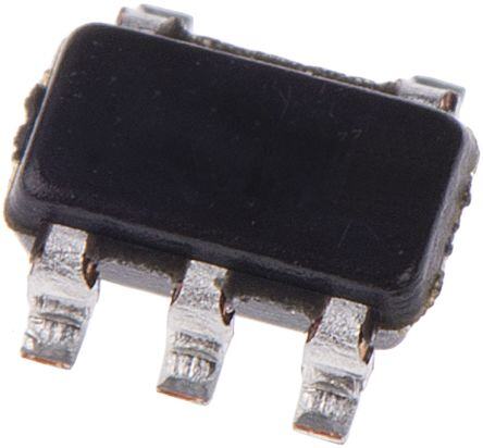
| 描述 | IC OPAMP CHOPPER 350KHZ SOT23-5运算放大器 - 运放 Lo Cost Prec CMOS Op Amp Zero Drift |
| 产品分类 | Linear - Amplifiers - Instrumentation, OP Amps, Buffer Amps集成电路 - IC |
| 品牌 | Texas Instruments |
| 产品手册 | http://www.ti.com/litv/sbos432e |
| 产品图片 |
|
| rohs | 符合RoHS无铅 / 符合限制有害物质指令(RoHS)规范要求 |
| 产品系列 | 放大器 IC,运算放大器 - 运放,Texas Instruments OPA330AIDBVT- |
| 数据手册 | |
| 产品型号 | OPA330AIDBVT |
| 产品目录页面 | |
| 产品种类 | 运算放大器 - 运放 |
| 供应商器件封装 | SOT-23-5 |
| 共模抑制比—最小值 | 100 dB |
| 关闭 | No Shutdown |
| 其它名称 | 296-25307-1 |
| 包装 | 剪切带 (CT) |
| 压摆率 | 0.16 V/µs |
| 商标 | Texas Instruments |
| 增益带宽生成 | 350 kHz |
| 增益带宽积 | 350kHz |
| 安装类型 | 表面贴装 |
| 安装风格 | SMD/SMT |
| 封装 | Reel |
| 封装/外壳 | SC-74A,SOT-753 |
| 封装/箱体 | SOT-23-5 |
| 工作温度 | -40°C ~ 125°C |
| 工作电源电压 | 1.8 V to 5.5 V |
| 工厂包装数量 | 250 |
| 放大器类型 | 零漂移 |
| 最大工作温度 | + 150 C |
| 最小工作温度 | - 40 C |
| 标准包装 | 1 |
| 电压-电源,单/双 (±) | 1.8 V ~ 5.5 V, ±0.9 V ~ 2.75 V |
| 电压-输入失调 | 8µV |
| 电流-电源 | 21µA |
| 电流-输入偏置 | 200pA |
| 电流-输出/通道 | 5mA |
| 电源电流 | 21 uA |
| 电路数 | 1 |
| 系列 | OPA330 |
| 设计资源 | http://www.digikey.com/product-highlights/cn/zh/texas-instruments-webench-design-center/3176 |
| 转换速度 | 0.16 V/us |
| 输入偏压电流—最大 | 500 pA |
| 输入参考电压噪声 | 0.3 uV |
| 输入补偿电压 | 50 uV |
| 输出电流 | 5 mA |
| 输出类型 | 满摆幅 |
| 通道数量 | 1 Channel |


- 商务部:美国ITC正式对集成电路等产品启动337调查
- 曝三星4nm工艺存在良率问题 高通将骁龙8 Gen1或转产台积电
- 太阳诱电将投资9.5亿元在常州建新厂生产MLCC 预计2023年完工
- 英特尔发布欧洲新工厂建设计划 深化IDM 2.0 战略
- 台积电先进制程称霸业界 有大客户加持明年业绩稳了
- 达到5530亿美元!SIA预计今年全球半导体销售额将创下新高
- 英特尔拟将自动驾驶子公司Mobileye上市 估值或超500亿美元
- 三星加码芯片和SET,合并消费电子和移动部门,撤换高东真等 CEO
- 三星电子宣布重大人事变动 还合并消费电子和移动部门
- 海关总署:前11个月进口集成电路产品价值2.52万亿元 增长14.8%


PDF Datasheet 数据手册内容提取
Product Sample & Technical Tools & Support & Reference Folder Buy Documents Software Community Design OPA330,OPA2330,OPA4330 SBOS432G–AUGUST2008–REVISEDAUGUST2016 OPAx330 50-μV V , 0.25-μV/°C, 35-μA CMOS Operational Amplifiers OS Zero-Drift Series 1 Features 3 Description • UnmatchedPricePerformance The OPA330 series of CMOS operational amplifiers 1 offer precision performance at a very competitive • LowOffsetVoltage:50 µV(Maximum) price. These devices are members of the Zero-Drift • ZeroDrift:0.25 µV/°C(Maximum) family of amplifiers which use a proprietary auto- • LowNoise:1.1µV ,0.1Hzto10Hz calibration technique to simultaneously provide low PP offset voltage (50-μV maximum) and near-zero drift • QuiescentCurrent:35µA(Maximum) over time and temperature at only 35 μA (maximum) • SupplyVoltage:1.8Vto5.5V ofquiescentcurrent.TheOPA330familyfeaturesrail- • Rail-to-RailInputandOutput to-rail input and output in addition to near-flat 1/f noise, making this amplifier ideal for many • InternalEMIFiltering applications and much easier to design into a system. • microSizePackages:DSBGA,SC70,VQFN These devices are optimized for low-voltage operation as low as 1.8 V (±0.9 V) and up to 5.5 V 2 Applications (±2.75V). • Battery-PoweredInstruments The OPA330 (single version) is available in the 5-pin • TemperatureMeasurements DSBGA, 5-pin SC70, 5-pin SOT-23, and 8-pin SOIC packages.TheOPA2330(dualversion)isofferedin3 • TransducerApplications mm × 3 mm, 8-pin SON, 8-pin VSSOP, and 8-pin • ElectronicScales SOIC packages. The OPA4330 is offered in the • MedicalInstrumentation standard 14-pin SOIC and 14-pin TSSOP packages, • HandheldTestEquipment as well as in the space-saving 14-pin VQFN package. All versions are specified for operation from –40°C to • CurrentSense 125°C. DeviceInformation(1) PARTNUMBER PACKAGE BODYSIZE(NOM) SOIC(8) 4.90mm×3.91mm SOT(5) 2.90mm×1.60mm OPA330 Bidirectional,Low-SideCurrentSense SC70(5) 2.00mm×1.25mm VCC DSBGA(5) 0.00mm×0.00mm VCC SOIC(8) 4.90mm×3.91mm – R5 OPA2330 VSSOP(8) 3.00mm×3.00mm + SON(8) 3.00mm×3.00mm SOIC(14) 8.65mm×3.91mm R6 ILOAD R2 OPA4330 TSSOP(14) 5.00mm×4.40mm VQFN(14) 3.50mm×3.50mm R1 + + (1) For all available packages, see the orderable addendum at VBUS ± RSHUNT – VOUT theendofthedatasheet. R3 VCC RL R4 Copyright © 2016,Texas Instruments Incorporated 1 An IMPORTANT NOTICE at the end of this data sheet addresses availability, warranty, changes, use in safety-critical applications, intellectualpropertymattersandotherimportantdisclaimers.PRODUCTIONDATA.
OPA330,OPA2330,OPA4330 SBOS432G–AUGUST2008–REVISEDAUGUST2016 www.ti.com Table of Contents 1 Features.................................................................. 1 8.4 DeviceFunctionalModes........................................14 2 Applications........................................................... 1 9 ApplicationandImplementation........................ 15 3 Description............................................................. 1 9.1 ApplicationInformation............................................15 4 RevisionHistory..................................................... 2 9.2 TypicalApplication..................................................17 9.3 SystemExamples...................................................19 5 DeviceComparisonTable..................................... 4 10 PowerSupplyRecommendations..................... 20 6 PinConfigurationsandFunctions....................... 4 11 Layout................................................................... 21 7 Specifications......................................................... 7 11.1 LayoutGuidelines.................................................21 7.1 AbsoluteMaximumRatings......................................7 11.2 LayoutExample....................................................22 7.2 ESDRatings..............................................................7 12 DeviceandDocumentationSupport................. 23 7.3 RecommendedOperatingConditions.......................7 7.4 ThermalInformation:OPA330..................................8 12.1 DeviceSupport ....................................................23 7.5 ThermalInformation:OPA2330................................8 12.2 DocumentationSupport .......................................24 7.6 ThermalInformation:OPA4330................................8 12.3 RelatedLinks........................................................24 7.7 ElectricalCharacteristics...........................................9 12.4 ReceivingNotificationofDocumentationUpdates24 7.8 TypicalCharacteristics............................................10 12.5 CommunityResources..........................................24 12.6 Trademarks...........................................................24 8 DetailedDescription............................................ 14 12.7 ElectrostaticDischargeCaution............................24 8.1 Overview.................................................................14 12.8 Glossary................................................................24 8.2 FunctionalBlockDiagram.......................................14 13 Mechanical,Packaging,andOrderable 8.3 FeatureDescription.................................................14 Information........................................................... 25 4 Revision History NOTE:Pagenumbersforpreviousrevisionsmaydifferfrompagenumbersinthecurrentversion. ChangesfromRevisionF(June2016)toRevisionG Page • ChangedPinFunctions:OPA330soeachpinhasaseparaterow....................................................................................... 4 • ChangedpositionofInputVoltageRange,CMRRparameterspecificationvaluesinElectricalCharacteristicstable..........9 • ChangedpositionofOpen-LoopGain,A parameterspecificationvaluesinElectricalCharacteristicstable.....................9 OL ChangesfromRevisionE(February2011)toRevisionF Page • AddedESDRatingstable,FeatureDescriptionsection,DeviceFunctionalModes,ApplicationandImplementation section,PowerSupplyRecommendationssection,Layoutsection,DeviceandDocumentationSupportsection,and Mechanical,Packaging,andOrderableInformationsection ................................................................................................. 1 • AddedcurrentpackagedesignatorstosecondparagraphofDescriptionsection ................................................................ 1 • RemovedPackageInformationtable,seePOAattheendofthedatasheet......................................................................... 1 • ChangedProductFamilyPackageComparisontabletoDeviceComparisontable;movedfrompage1ofdocument........4 ChangesfromRevisionD(June2010)toRevisionE Page • ChangeddocumentstatusfromMixedStatustoProductionData........................................................................................ 1 • Deletedfootnote2fromthePackageInformationtable......................................................................................................... 1 • Addedremainingthermalinformationdata............................................................................................................................. 8 2 SubmitDocumentationFeedback Copyright©2008–2016,TexasInstrumentsIncorporated ProductFolderLinks:OPA330 OPA2330 OPA4330
OPA330,OPA2330,OPA4330 www.ti.com SBOS432G–AUGUST2008–REVISEDAUGUST2016 ChangesfromRevisionC(October2009)toRevisionD Page • AddedlastApplicationsbullet................................................................................................................................................. 1 • Deletedfootnote2andshadingfromallpackagesexceptQFN-14;movedWCSP-5,SOIC-14,andTSSOP-14 packagestoProductionDatastatus;andaddedpackagemarkinginformationtoPackageInformationtable.....................1 • Deletedfootnote1fromProductFamilyPackageComparisontable.................................................................................... 4 • MovedTSSOP-14thermalresistancetoMSOP-8,SOIC-8thermalresistanceparameterinElectricalCharacteristics table........................................................................................................................................................................................ 9 • DeletedSOIC-14andQFN-14rowsfromTemperatureRangesectioninElectricalCharacteristicstable........................... 9 • AddedOPA330YFF,OPA4330InputBiasCurrentparametertoElectricalCharacteristicstable......................................... 9 • AddedInputVoltageRange,OPA330YFF,OPA4330Common-ModeRejectionRatioparametertoElectrical Characteristicstable............................................................................................................................................................... 9 Copyright©2008–2016,TexasInstrumentsIncorporated SubmitDocumentationFeedback 3 ProductFolderLinks:OPA330 OPA2330 OPA4330
OPA330,OPA2330,OPA4330 SBOS432G–AUGUST2008–REVISEDAUGUST2016 www.ti.com 5 Device Comparison Table NOOF PACKAGE-LEADS DEVICE CHANNELS DSBGA SOIC SOT SC70 VSSOP SON VQFN TSSOP OPA330 1 5 8 5 5 — — — — OPA2330 2 — 8 — — 8 8 — — OPA4330 4 — 14 — — — — 14 14 6 Pin Configurations and Functions OPA330:DPackage 8-PinSOIC OPA330:DCKPackage TopView 5-PinSC70 TopView NC(1) 1 8 NC(1) +IN 1 5 V+ -IN 2 7 V+ V- 2 +IN 3 6 OUT -IN 3 4 OUT V- 4 5 NC(1) (1) NCdenotesnointernalconnection. OPA330:YFFPackage 5-PinDSBGA TopView OPA330:DBVPackage 5-PinSOT-23 C3 C1 TopView OUT IN- B2 V - OUT 1 5 V+ S A3 A1 V- 2 VS+ IN+ +IN 3 4 -IN PinFunctions:OPA330 PIN I/O DESCRIPTION NAME SOIC SOT-23 SC70 DSBGA –IN 2 4 3 C1 I Negative(inverting)input +IN 3 3 1 A1 I Positive(noninverting)input NC 1,5,8 — — — — Nointernalconnection(canbeleftfloating) OUT 6 1 4 C3 O Output V– 4 2 2 — — Negative(lowest)powersupply V+ 7 5 5 — — Positive(highest)powersupply V — — — B2 — Negative(lowest)powersupply S– V — — — A3 — Positive(highest)powersupply S+ 4 SubmitDocumentationFeedback Copyright©2008–2016,TexasInstrumentsIncorporated ProductFolderLinks:OPA330 OPA2330 OPA4330
OPA330,OPA2330,OPA4330 www.ti.com SBOS432G–AUGUST2008–REVISEDAUGUST2016 OPA2330:DandDGKPackages 8-PinSOICand8-PinVSSOP OPA2330:DRBPackage TopView 8-PinSON TopView OUT A 1 8 V+ A -IN A 2 7 OUT B OUTA 1 8 V+ Exposed B +IN A 3 6 -IN B -INA 2 Thermal 7 OUTB Die Pad V- 4 5 +IN B +INA 3 on 6 -IN B Underside(1) V- 4 5 +IN B (1) ConnectthermaldiepadtoV–. PinFunctions:OPA2330 PIN SOIC, I/O DESCRIPTION NAME SON VSSOP –INA 2 2 I Negative(inverting)inputsignal,channelA +INA 3 3 I Positive(noninverting)inputsignal,channelA –INB 6 6 I Negative(inverting)inputsignal,channelB +INB 5 5 I Positive(noninverting)inputsignal,channelB OUTA 1 1 O OutputchannelA OUTB 7 7 O OutputchannelB V– 4 4 — Negative(lowest)powersupply V+ 8 8 — Positive(highest)powersupply Copyright©2008–2016,TexasInstrumentsIncorporated SubmitDocumentationFeedback 5 ProductFolderLinks:OPA330 OPA2330 OPA4330
OPA330,OPA2330,OPA4330 SBOS432G–AUGUST2008–REVISEDAUGUST2016 www.ti.com OPA4330:DPackage 14-PinSOIC OPA4330:PWPackage TopView 14-PinTSSOP TopView OUT A 1 14 OUT D OUT A 1 14 OUT D -IN A 2 13 -IN D A D -IN A 2 13 -IN D +IN A 3 12 +IN D +IN A 3 12 +IN D V+ 4 11 V- V+ 4 11 V- +IN B 5 10 +IN C B C +IN B 5 10 +IN C -IN B 6 9 -IN C -IN B 6 9 -IN C OUT B 7 8 OUT C OUT B 7 8 OUT C OPA4330:RGYPackage 14-PinVQFN TopView A D T T U U O O 1 14 -INA 2 13 -IN D +INA 3 Exposed 12 +IN D Thermal Die V+ 4 Pad on 11 V- (1) Underside +IN B 5 10 +IN C -IN B 6 9 -IN C 7 8 B C T T U U O O (1) ConnectthermaldiepadtoV–. PinFunctions:OPA4330 PIN I/O DESCRIPTION NAME SOIC TSSOP VQFN –INA 2 2 2 I Negative(inverting)inputsignal,channelA +INA 3 3 3 I Positive(noninverting)inputsignal,channelA –INB 6 6 6 I Negative(inverting)inputsignal,channelB +INB 5 5 5 I Positive(noninverting)inputsignal,channelB –INC 9 9 9 I Negative(inverting)inputsignal,channelC +INC 10 10 10 I Positive(noninverting)inputsignal,channelC –IND 13 13 13 I Negative(inverting)inputsignal,channelD +IND 12 12 12 I Positive(noninverting)inputsignal,channelD OUTA 1 1 1 O OutputchannelA OUTB 7 7 7 O OutputchannelB OUTC 8 8 8 O OutputchannelC OUTD 14 14 14 O OutputchannelD V– 11 11 11 — Negative(lowest)powersupply V+ 4 4 4 — Positive(highest)powersupply 6 SubmitDocumentationFeedback Copyright©2008–2016,TexasInstrumentsIncorporated ProductFolderLinks:OPA330 OPA2330 OPA4330
OPA330,OPA2330,OPA4330 www.ti.com SBOS432G–AUGUST2008–REVISEDAUGUST2016 7 Specifications 7.1 Absolute Maximum Ratings overoperatingfree-airtemperaturerange(unlessotherwisenoted)(1) MIN MAX UNIT Supply,V =(V+)–(V–) 7 V S Voltage Signalinputterminals(2)(TBDshouldterminalbepin?) (V–)–0.3 (V+)+0.3 V Signalinputterminals(2) –10 10 mA Current Outputshort-circuit(3) Continuous Operatingrange,T –40 150 °C A Temperature Junction,T 150 °C J Storage,T –65 150 °C stg (1) StressesbeyondthoselistedunderAbsoluteMaximumRatingsmaycausepermanentdamagetothedevice.Thesearestressratings only,whichdonotimplyfunctionaloperationofthedeviceattheseoranyotherconditionsbeyondthoseindicatedunderRecommended OperatingConditions.Exposuretoabsolute-maximum-ratedconditionsforextendedperiodsmayaffectdevicereliability. (2) Inputterminalsarediode-clampedtothepower-supplyrails.Inputsignalsthatcanswingmorethan0.3Vbeyondthesupplyrailsshould becurrentlimitedto10mAorless. (3) Short-circuittoground,oneamplifierperpackage. 7.2 ESD Ratings VALUE UNIT Human-bodymodel(HBM),perANSI/ESDA/JEDECJS-001(1) ±4000 V Electrostaticdischarge Charged-devicemodel(CDM),perJEDECspecificationJESD22-C101(2) ±1000 V (ESD) Machinemodel(MM) ±400 (1) JEDECdocumentJEP155statesthat500-VHBMallowssafemanufacturingwithastandardESDcontrolprocess. (2) JEDECdocumentJEP157statesthat250-VCDMallowssafemanufacturingwithastandardESDcontrolprocess. 7.3 Recommended Operating Conditions overoperatingfree-airtemperaturerange(unlessotherwisenoted) MIN NOM MAX UNIT (V+)–(V–) Supplyvoltage ±0.9(1.8) ±2.5(5) ±2.75(5.5) V T Specifiedtemperature –40 25 125 °C A Copyright©2008–2016,TexasInstrumentsIncorporated SubmitDocumentationFeedback 7 ProductFolderLinks:OPA330 OPA2330 OPA4330
OPA330,OPA2330,OPA4330 SBOS432G–AUGUST2008–REVISEDAUGUST2016 www.ti.com 7.4 Thermal Information: OPA330 OPA330 THERMALMETRIC(1) D(SOIC) DBV(SOT-23) DCK(SC70) YFF(DSBGA) UNIT 8PINS 5PINS 5PINS 5PINS RθJA Junction-to-ambientthermalresistance 140.1 220.8 298.4 130 °C/W RθJC(top) Junction-to-case(top)thermalresistance 89.8 97.5 65.4 54 °C/W RθJB Junction-to-boardthermalresistance 80.6 61.7 97.1 51 °C/W ψJT Junction-to-topcharacterizationparameter 28.7 7.6 0.8 1 °C/W ψJB Junction-to-boardcharacterizationparameter 80.1 61.1 95.5 50 °C/W (1) Formoreinformationabouttraditionalandnewthermalmetrics,seetheSemiconductorandICPackageThermalMetricsapplication report. 7.5 Thermal Information: OPA2330 OPA2330 THERMALMETRIC(1) D(SOIC) DGK(VSSOP) DRB(SON) UNIT 8PINS 8PINS 8PINS RθJA Junction-to-ambientthermalresistance 124 180.3 46.7 °C/W RθJC(top) Junction-to-case(top)thermalresistance 73.7 48.1 26.3 °C/W RθJB Junction-to-boardthermalresistance 64.4 100.9 22.2 °C/W ψJT Junction-to-topcharacterizationparameter 18 2.4 1.6 °C/W ψJB Junction-to-boardcharacterizationparameter 63.9 99.3 22.3 °C/W RθJC(bot) Junction-to-case(bottom)thermalresistance — — 10.1 °C/W (1) Formoreinformationabouttraditionalandnewthermalmetrics,seetheSemiconductorandICPackageThermalMetricsapplication report. 7.6 Thermal Information: OPA4330 OPA4330 THERMALMETRIC(1) D(SOIC) PW(TSSOP) RGY(VQFN) UNIT 14PINS 14PINS 14PINS RθJA Junction-to-ambientthermalresistance 83.8 120.8 49.2 °C/W RθJC(top) Junction-to-case(top)thermalresistance 70.7 34.3 75.3 °C/W RθJB Junction-to-boardthermalresistance 59.5 62.8 61.9 °C/W ψJT Junction-to-topcharacterizationparameter 11.6 1 1.2 °C/W ψJB Junction-to-boardcharacterizationparameter 37.7 56.5 19.3 °C/W RθJC(bot) Junction-to-case(bottom)thermalresistance — — 4.6 °C/W (1) Formoreinformationabouttraditionalandnewthermalmetrics,seetheSemiconductorandICPackageThermalMetricsapplication report. 8 SubmitDocumentationFeedback Copyright©2008–2016,TexasInstrumentsIncorporated ProductFolderLinks:OPA330 OPA2330 OPA4330
OPA330,OPA2330,OPA4330 www.ti.com SBOS432G–AUGUST2008–REVISEDAUGUST2016 7.7 Electrical Characteristics atT =25°C,R =10kΩconnectedtomidsupply,V =1.8Vto5.5V,andV =V =midsupply(unlessotherwisenoted) A L S CM OUT PARAMETER TESTCONDITIONS MIN TYP MAX UNIT OFFSETVOLTAGE VOS Inputoffsetvoltage VS=5V 8 50 µV Inputoffsetvoltage dVOS/dT versustemperature AtTA=–40°Cto+125°C 0.02 0.25 µV/°C Inputoffsetvoltage PSRR versuspowersupply AtTA=–40°Cto+125°C 1 10 µV/V Long-termstability(1) VS=1.8Vto5.5V See(1) Channelseparation,dc 0.1 µV/V INPUTBIASCURRENT ±200 ±500 pA At25°C OPA330YFF, IB Inputbiascurrent OPA4330 ±70 ±300 pA AtTA=–40°Cto+125°C ±300 pA ±400 ±1000 pA IOS Inputoffsetcurrent At25°C OPA330YFF, ±140 ±600 pA OPA4330 NOISE Inputvoltagenoise en density f=1kHz 55 nV/√Hz f=0.01Hzto1Hz 0.3 µVPP Inputvoltagenoise f=0.1Hzto10Hz 1.1 µVPP in Inputcurrentnoise f=10Hz 100 fA/√Hz INPUTVOLTAGERANGE Common-modevoltage VCM range (V–)–0.1 (V+)+0.1 V AtTA=–40°Cto+125°C, 100 115 dB (V–)–0.1V<VCM<(V+)+0.1V Common-moderejection CMRR ratio AtTA=–40°Cto+125°C, 100 115 dB (V–)–0.1V<VCM<(V+)+0.1V, OPA330YFF, VS=5.5V OPA4330 100 115 dB INPUTCAPACITANCE Differential 2 pF Common-mode 4 pF OPEN-LOOPGAIN AOL Open-loopvoltagegain A(Vt–T)A+=1–0400m°CVt<o+V1O2<5°(CV,+)–100mV,RL=10kΩ 100 115 dB FREQUENCYRESPONSE GBW Gain-bandwidthproduct CL=100pF 350 kHz SR Slewrate G=+1 0.16 V/µs OUTPUT Voltageoutputswing fromrail AtTA=–40°Cto+125°C 30 100 mV ISC Short-circuitcurrent ±5 mA CL Capacitiveloaddrive SeeTypicalCharacteristics Open-loopoutput impedance f=350kHz,IO=0mA 2 kΩ POWERSUPPLY VS Specifiedvoltagerange 1.8 5.5 V Quiescentcurrentper IQ amplifier AtTA=–40°Cto+125°C,IO=0mA 21 35 µA Turnontime VS=5V 100 µs (1) 300-hourlifetestat150°Cdemonstratedrandomlydistributedvariationofapproximately1µV. Copyright©2008–2016,TexasInstrumentsIncorporated SubmitDocumentationFeedback 9 ProductFolderLinks:OPA330 OPA2330 OPA4330
OPA330,OPA2330,OPA4330 SBOS432G–AUGUST2008–REVISEDAUGUST2016 www.ti.com 7.8 Typical Characteristics AtT =25°C,C =0pF,R =10kΩconnectedtomidsupply,andV =V =midsupply,unlessotherwisenoted. A L L CM OUT Table1.TableofGraphs DESCRIPTION FIGURENO. OffsetVoltageProductionDistribution Figure1 Open-LoopGainvsFrequency Figure2 Common-ModeRejectionRatiovsFrequency Figure3 Power-SupplyRejectionRatiovsFrequency Figure4 OutputVoltageSwingvsOutputCurrent Figure5 InputBiasCurrentvsCommon-ModeVoltage Figure6 InputBiasCurrentvsTemperature Figure7 QuiescentCurrentvsTemperature Figure8 Large-SignalStepResponse Figure9 Small-SignalStepResponse Figure10 PositiveOvervoltageRecovery Figure11 NegativeOvervoltageRecovery Figure12 SettlingTimevsClosed-LoopGain Figure13 Small-SignalOvershootvsLoadCapacitance Figure14 0.1-Hzto10-HzNoise Figure15 CurrentandVoltageNoiseSpectralDensityvsFrequency Figure16 InputBiasCurrentvsInputDifferentialVoltage Figure17 10 SubmitDocumentationFeedback Copyright©2008–2016,TexasInstrumentsIncorporated ProductFolderLinks:OPA330 OPA2330 OPA4330
OPA330,OPA2330,OPA4330 www.ti.com SBOS432G–AUGUST2008–REVISEDAUGUST2016 120 250 100 200 80 150 Phase Population A(dB)OL 6400 Gain 15000 Phase ()° 20 0 0 -50 -20 -100 0 0 0 0 0 0 0 0 0 0 0 0 0 0 0 0 0 10 100 1k 10k 100k 1M 0 0 0 0 0 0 0 0 0 0 0 0 0 0 0 0 24. 21. 18. 15. 12. -9. -6. -3. 3. 6. 9. 12. 15. 18. 21. 24. Frequency (Hz) - - - - - Offset Voltage (mV) Figure1.OffsetVoltageProductionDistribution Figure2.Open-LoopGainvsFrequency 140 120 +PSRR 120 100 100 -PSRR 80 B) B) R (d 80 R (d 60 R R M 60 S C P 40 40 20 20 0 0 1 10 100 1k 10k 100k 1M 1 10 100 1k 10k 100k 1M Frequency (Hz) Frequency (Hz) Figure3.Common-ModeRejectionRatiovsFrequency Figure4.Power-SupplyRejectionRatiovsFrequency 3 210 V =±2.75V S V =±0.9V 205 S 2 200 -40°C -IB V) 1 195 wing ( +125°C +25°C A) 190 put S 0 +25°C -40°C I(pB -190 Out -1 +125°C -195 +I -2 +25°C -200 B -205 -40°C -3 -210 0 1 2 3 4 5 6 7 8 9 10 0 1 2 3 4 5 Output Current (mA) Common-Mode Voltage (V) Figure5.OutputVoltageSwingvsOutputCurrent Figure6.InputBiasCurrentvsCommon-ModeVoltage Copyright©2008–2016,TexasInstrumentsIncorporated SubmitDocumentationFeedback 11 ProductFolderLinks:OPA330 OPA2330 OPA4330
OPA330,OPA2330,OPA4330 SBOS432G–AUGUST2008–REVISEDAUGUST2016 www.ti.com 250 25 -I B 200 V = 5.5V S -I 150 B 20 100 V = 1.8V S 50 15 A) V = 5.5V A) p 0 S m ( V = 1.8V ( B S Q I -50 I 10 -100 -150 +IB 5 -200 +I -250 B 0 -50 -25 0 25 50 75 100 125 -50 -25 0 25 50 75 100 125 Temperature (°C) Temperature (°C) Figure7.InputBiasCurrentvsTemperature Figure8.QuiescentCurrentvsTemperature G = 1 G = +1 R = 10kW R = 10kW L L v) div) V/di mV/ Voltage (1 oltage (50 Output utput V O Time (50ms/div) Time (5ms/div) Figure9.Large-SignalStepResponse Figure10.Small-SignalStepResponse v di 2V/ 0 Input Input v di Output 2V/ 0 v 0 10kW V/di 10kW 1 +2.5V +2.5V 1kW 1kW v 0 Output V/di OPA330 OPA330 1 -2.5V -2.5V Time (50ms/div) Time (50ms/div) Figure11.PositiveOvervoltageRecovery Figure12.NegativeOvervoltageRecovery 12 SubmitDocumentationFeedback Copyright©2008–2016,TexasInstrumentsIncorporated ProductFolderLinks:OPA330 OPA2330 OPA4330
OPA330,OPA2330,OPA4330 www.ti.com SBOS432G–AUGUST2008–REVISEDAUGUST2016 600 40 4V Step 35 500 30 mme (s) 400 ot (%) 25 g Ti 300 sho 20 ettlin 200 Over 15 S 0.001% 10 100 5 0.01% 0 0 1 10 100 10 100 1000 Gain (dB) Load Capacitance (pF) Figure13.SettlingTimevsClosed-LoopGain Figure14.Small-SignalOvershootvsLoadCapacitance 1000 1000 )z C 500nV/div ÖVoltage Noise (nV/H 100 Continues withCV nuoorltr ae1gn/fet ( NfNliocoikisseeer) noise. 100 urrent Noise (fA/)HzÖ 10 10 1s/div 1 10 100 1k 10k Frequency (Hz) Figure15.0.1-Hzto10-HzNoise Figure16.CurrentandVoltageNoiseSpectralDensityvs Frequency 50 Normal Operating Range 40 (see theInput Differential 30 Voltagesection in the A) Applications Information) m 20 ent ( 10 Curr 0 s a -10 Bi ut -20 p n I -30 Over-Driven Condition Over-Driven Condition -40 -50 -1V -800 -600 -400 -200 0 200 400 600 800 Input Differential Voltage (mV) Figure17.InputBiasCurrentvsInputDifferentialVoltage Copyright©2008–2016,TexasInstrumentsIncorporated SubmitDocumentationFeedback 13 ProductFolderLinks:OPA330 OPA2330 OPA4330
OPA330,OPA2330,OPA4330 SBOS432G–AUGUST2008–REVISEDAUGUST2016 www.ti.com 8 Detailed Description 8.1 Overview The OPA330 family of Zerø-Drift amplifiers feature a proprietary auto-calibration technique to simultaneously achieve near-zero drift over time and temperature at only 35 µA (maximum) of quiescent current while also providing low offset voltage (50 µV maximum). These devices are unity-gain stable, precision operational amplifiers free from unexpected output and phase reversal. The OPA330 series are also optimized for low- voltage,single-supplyoperation:aslowas1.8V(±0.9V)andupto5.5V(±2.75V). The proprietary Zerø-Drift circuitry lowers the 1/f noise component as well as offers the advantage of low input offsetvoltageovertimeandtemperature.TheOPA330seriesofoperationalamplifiersareidealforcost-sensitive applicationsandapplicationsthatoperatewithoutregulationdirectlyfrombatterypower. 8.2 Functional Block Diagram C2 Notch CHOP1 GM1 CHOP2 Filter GM2 GM3 +IN OUT -IN C1 GM_FF Copyright © 2016, Texas Instruments Incorporated 8.3 Feature Description The OPA33x family is unity-gain stable and free from unexpected output phase reversal. These devices use a proprietary auto-calibration technique to provide low offset voltage and very low drift over time and temperature. For lowest offset voltage and precision performance, optimize circuit layout, and mechanical conditions. Avoid temperature gradients that create thermoelectric (Seebeck) effects in the thermocouple junctions formed from connecting dissimilar conductors. Cancel these thermally-generated potentials by assuringtheyareequalonbothinputterminals.Otherlayoutanddesignconsiderationsinclude: • Uselowthermoelectric-coefficientconditions(avoiddissimilarmetals). • Thermallyisolatecomponentsfrompowersuppliesorotherheatsources. • Shieldoperationalamplifierandinputcircuitryfromaircurrents,suchascoolingfans. Following these guidelines reduces the likelihood of junctions being at different temperatures, which can causethermoelectricvoltagedriftof0.1 µV/°Corhigher,dependingonmaterialsused. 8.4 Device Functional Modes The OPAx330 has a single functional mode and is operational when the power-supply voltage is greater than 1.8V(±0.9V).Themaximumpower-supplyvoltagefortheOPAx330is5.5V(±2.75V). 14 SubmitDocumentationFeedback Copyright©2008–2016,TexasInstrumentsIncorporated ProductFolderLinks:OPA330 OPA2330 OPA4330
OPA330,OPA2330,OPA4330 www.ti.com SBOS432G–AUGUST2008–REVISEDAUGUST2016 9 Application and Implementation NOTE Information in the following applications sections is not part of the TI component specification, and TI does not warrant its accuracy or completeness. TI’s customers are responsible for determining suitability of components for their purposes. Customers should validateandtesttheirdesignimplementationtoconfirmsystemfunctionality. 9.1 Application Information The OPA330, OPA2330, and OPA4330 are unity-gain stable, precision operational amplifiers free from unexpected output and phase reversal. The use of proprietary Zerø-Drift circuitry gives the benefit of low input offset voltage over time and temperature, as well as lowering the 1/f noise component. As a result of the high PSRR, these devices work well in applications that run directly from battery power without regulation. The OPA330 family is optimized for low-voltage, single-supply operation. These miniature, high-precision, low quiescent current amplifiers offer high-impedance inputs that have a common-mode range 100 mV beyond the supplies and a rail-to-rail output that swings within 100 mV of the supplies under normal test conditions. The OPA330seriesareprecisionamplifiersforcost-sensitiveapplications. 9.1.1 OperatingVoltage The OPA330 series operational amplifiers can be used with single or dual supplies from an operating range of V = 1.8 V (±0.9 V) up to 5.5 V (±2.75 V). Supply voltages greater than 7 V can permanently damage the device S (see Absolute Maximum Ratings). Key parameters that vary over the supply voltage or temperature range are showninTypicalCharacteristics. 9.1.2 InputVoltage The OPA330, OPA2330, and OPA4330 input common-mode voltage range extends 0.1 V beyond the supply rails. The OPA330 is designed to cover the full range without the troublesome transition region found in some otherrail-to-railamplifiers. Typically, input bias current is approximately 200 pA. Input voltages exceeding the power supplies however, can cause excessive current to flow into or out of the input pins. Momentary voltages greater than the power supply can be tolerated if the input current is limited to 10 mA. This limitation is easily accomplished with an input resistor,asshowninFigure18. Current-limiting resistor required if input voltage exceeds supply rails by ³0.3V. +5V I OVERLOAD 10mAmax OPA330 V OUT V IN 5kW Copyright © 2016,Texas Instruments Incorporated Figure18. InputCurrentProtection 9.1.3 InputDifferentialVoltage The typical input bias current of the OPA330 during normal operation is approximately 200 pA. In over-driven conditions,thebiascurrentcanincreasesignificantly(seeFigure17).Themostcommoncauseofanover-driven conditionoccurswhentheoperationalamplifierisoutsideofthelinearrangeofoperation.Whentheoutputofthe operational amplifier is driven to one of the supply rails the feedback loop requirements cannot be satisfied and a differential input voltage develops across the input pins. This differential input voltage results in activation of parasitic diodes inside the front end input chopping switches that combine with 10-kΩ electromagnetic interference (EMI) filter resistors to create the equivalent circuit illustrated in Figure 19. Notice that the input bias currentremainswithinspecificationwithinthelinearregion. Copyright©2008–2016,TexasInstrumentsIncorporated SubmitDocumentationFeedback 15 ProductFolderLinks:OPA330 OPA2330 OPA4330
OPA330,OPA2330,OPA4330 SBOS432G–AUGUST2008–REVISEDAUGUST2016 www.ti.com Application Information (continued) 10kW Clamp +In CORE -In 10kW Copyright © 2016,Texas Instruments Incorporated Figure19. EquivalentInputCircuit 9.1.4 InternalOffsetCorrection The OPA330, OPA2330, and OPA4330 operational amplifiers use an auto-calibration technique with a time- continuous, 125-kHz operational amplifier in the signal path. This amplifier is zero-corrected every 8 µs using a proprietary technique. Upon power up, the amplifier requires approximately 100 µs to achieve specified V OS accuracy.Thisdesignhasnoaliasingorflickernoise. 9.1.5 EMISusceptibilityandInputFiltering OperationalamplifiersvaryintheirsusceptibilitytoEMI.IfconductedEMIenterstheoperationalamplifier,theDC offset observed at the amplifier output may shift from its nominal value while the EMI is present. This shift is a result of signal rectification associated with the internal semiconductor junctions. While all operational amplifier pin functions can be affected by EMI, the input pins are likely to be the most susceptible. The OPA330 operational amplifier family incorporates an internal input low-pass filter that reduces the amplifier response to EMI.Bothcommon-modeanddifferentialmodefilteringareprovidedbytheinputfilter.Thefilterisdesignedfora cutofffrequencyofapproximately8MHz(–3dB),witharolloffof20dBperdecade. 9.1.6 AchievingOutputSwingtotheOperationalAmplifierNegativeRail Some applications require output voltage swings from 0 V to a positive full-scale voltage (such as 2.5 V) with excellent accuracy. With most single-supply operational amplifiers, problems arise when the output signal approaches 0 V, near the lower output swing limit of a single-supply operational amplifier. A good single-supply operational amplifier may swing close to single-supply ground, but does not reach ground. The output of the OPA330, OPA2330, and OPA4330 can be made to swing to ground, or slightly below, on a single-supply power source. To do so requires the use of another resistor and an additional, more negative, power supply than the operational amplifier negative supply. A pulldown resistor may be connected between the output and the additional negative supply to pull the output down below the value that the output would otherwise achieve, as showninFigure20. V+ = +5V OPA330 V OUT V IN R = 20kW P OpAmp V-= GND -5V Additional Negative Supply Copyright © 2016,Texas Instruments Incorporated Figure20. ForV RangetoGround OUT 16 SubmitDocumentationFeedback Copyright©2008–2016,TexasInstrumentsIncorporated ProductFolderLinks:OPA330 OPA2330 OPA4330
OPA330,OPA2330,OPA4330 www.ti.com SBOS432G–AUGUST2008–REVISEDAUGUST2016 Application Information (continued) The OPA330, OPA2330, and OPA4330 have an output stage that allows the output voltage to be pulled to its negative supply rail, or slightly below, using the technique previously described. This technique only works with some types of output stages. The OPA330, OPA2330, and OPA4330 have been characterized to perform with this technique; the recommended resistor value is approximately 20 kΩ. This configuration increases the current consumption by several hundreds of microamps. Accuracy is excellent down to 0 V and as low as –2 mV. Limiting and nonlinearity occur below –2 mV, but excellent accuracy returns as the output is again driven above –2 mV. Lowering the resistance of the pulldown resistor allows the operational amplifier to swing even further below the negative rail. Resistances as low as 10 kΩ can be used to achieve excellent accuracy down to –10mV. 9.1.7 Photosensitivity Although the OPA330 YFF package has a protective backside coating that reduces the amount of light exposure on the die, unless fully shielded, ambient light can reach the active region of the device. Input bias current for the packageisspecifiedintheabsenceoflight.Dependingontheamountoflightexposureinagivenapplication,an increase in bias current, and possible increases in offset voltage should be expected. Fluorescent lighting may introduce noise or hum because of the time-varying light output. Best layout practices include end-product packagingthatprovidesshieldingfrompossiblelightsourcesduringoperation. 9.2 Typical Application 9.2.1 BidirectionalCurrent-Sensing This single-supply, low-side, bidirectional current-sensing solution detects load currents from –1 A to 1 A. The single-ended output spans from 110 mV to 3.19 V. This design uses the OPA2330 because of its low offset voltageandrail-to-railinputandoutput.Oneoftheamplifiersisconfiguredasadifferenceamplifierandtheother providesthereferencevoltage. Figure21showsthesolution. VCC VREF VCC R5 + U1B R6 ILOAD R2 + VBUS – + R1 + VSHUNT RSHUNT VOUT – U1A R3 VCC RL R4 Copyright © 2016, Texas Instruments Incorporated Figure21. BidirectionalCurrent-SensingSchematic Copyright©2008–2016,TexasInstrumentsIncorporated SubmitDocumentationFeedback 17 ProductFolderLinks:OPA330 OPA2330 OPA4330
OPA330,OPA2330,OPA4330 SBOS432G–AUGUST2008–REVISEDAUGUST2016 www.ti.com Typical Application (continued) 9.2.1.1 DesignRequirements Thissolutionhasthefollowingrequirements: • Supplyvoltage:3.3V • Input: –1Ato1A • Output:1.65V ±1.54V(110mVto3.19V) 9.2.1.2 DetailedDesignProcedure Theloadcurrent,I ,flowsthroughtheshuntresistor(R )todeveloptheshuntvoltage,V .Theshunt LOAD SHUNT SHUNT voltage is then amplified by the difference amplifier, which consists of U1A and R through R . The gain of the 1 4 difference amplifier is set by the ratio of R to R . To minimize errors, set R = R and R = R . The reference 4 3 2 4 1 3 voltage,V ,issuppliedbybufferingaresistordividerusingU1B.ThetransferfunctionisgivenbyEquation1. REF V = V ´Gain + V OUT SHUNT Diff_Amp REF where V = I ´R • SHUNT LOAD SHUNT R Gain = 4 Diff_Amp R • 3 R V = V ´ 6 REF CC R +R • 5 6 (1) There are two types of errors in this design: offset and gain. Gain errors are introduced by the tolerance of the shunt resistor and the ratios of R to R and, similarly, R to R . Offset errors are introduced by the voltage 4 3 2 1 divider (R and R ) and how closely the ratio of R /R matches R /R . The latter value impacts the CMRR of the 5 6 4 3 2 1 differenceamplifier,whichultimatelytranslatestoanoffseterror. Because this is a low-side measurement, the value of V is the ground potential for the system load. SHUNT Therefore, it is important to place a maximum value on V . In this design, the maximum value for V is SHUNT SHUNT set to 100 mV. Equation 2 calculates the maximum value of the shunt resistor given a maximum shunt voltage of 100mVandmaximumloadcurrentof1A. R = VSHUNT(Max) = 100 mV = 100 mW SHUNT(Max) I 1A LOAD(Max) (2) The tolerance of R is directly proportional to cost. For this design, a shunt resistor with a tolerance of 0.5% SHUNT wasselected.Ifgreateraccuracyisrequired,selecta0.1%resistororbetter. Theloadcurrentisbidirectional;therefore,theshuntvoltagerangeis –100mVto100mV.Thisvoltageisdivided down by R and R before reaching the operational amplifier, U1A. Take care to ensure that the voltage present 1 2 at the noninverting node of U1A is within the common-mode range of the device. Therefore, it is important to use an operational amplifier, such as the OPA330, that has a common-mode range that extends below the negative supply voltage. Finally, to minimize offset error, note that the OPA330 has a typical offset voltage of merely ±8µV(±50µVmaximum). Given a symmetric load current of –1 A to 1 A, the voltage divider resistors (R and R ) must be equal. To be 5 6 consistent with the shunt resistor, a tolerance of 0.5% was selected. To minimize power consumption, 10-kΩresistorswereused. To set the gain of the difference amplifier, the common-mode range and output swing of the OPA330 must be considered. Equation 3 and Equation 4 depict the typical common-mode range and maximum output swing, respectively,oftheOPA330givena3.3-Vsupply. –100mV<V <3.4V (3) CM 100mV<V <3.2V (4) OUT ThegainofthedifferenceamplifiercannowbecalculatedasshowninEquation5. V -V 3.2 V-100 mV V GainDiff_Amp= R OUT_M´ax(I OU-T_IMin) = 100 mW´[1A-(-1A)] = 15.5 V SHUNT MAX MIN (5) 18 SubmitDocumentationFeedback Copyright©2008–2016,TexasInstrumentsIncorporated ProductFolderLinks:OPA330 OPA2330 OPA4330
OPA330,OPA2330,OPA4330 www.ti.com SBOS432G–AUGUST2008–REVISEDAUGUST2016 Typical Application (continued) The resistor value selected for R and R was 1 kΩ. 15.4 kΩ was selected for R and R because it is the 1 3 2 4 neareststandardvalue.Therefore,theidealgainofthedifferenceamplifieris15.4V/V. The gain error of the circuit primarily depends on R through R . As a result of this dependence, 0.1% resistors 1 4 were selected. This configuration reduces the likelihood that the design requires a two-point calibration. A simple one-pointcalibration,ifdesired,removestheoffseterrorsintroducedbythe0.5%resistors. 9.2.1.3 ApplicationCurve 3.30 V) e ( g a olt1.65 V ut p ut O 0 -1.0 -0.5 0 0.5 1.0 Input Current (A) Figure22.BidirectionalCurrent-SensingCircuitPerformance: OutputVoltagevsInputCurrent 9.3 System Examples 9.3.1 SingleOperationalAmplifierBridgeAmplifier Figure23showsthebasicconfigurationforabridgeamplifier. V EX R 1 +5V R R R R OPA330 V OUT R 1 V REF Copyright © 2016,Texas Instruments Incorporated Figure23. SingleOperationalAmplifierBridgeAmplifierSchematic Copyright©2008–2016,TexasInstrumentsIncorporated SubmitDocumentationFeedback 19 ProductFolderLinks:OPA330 OPA2330 OPA4330
OPA330,OPA2330,OPA4330 SBOS432G–AUGUST2008–REVISEDAUGUST2016 www.ti.com System Examples (continued) 9.3.2 Low-SideCurrentMonitor Alow-sidecurrentshuntmonitorisshowninFigure24. R are operational resistors used to isolate the ADS1100 from the noise of the digital I2C bus. Because the N ADS1100 is a 16-bit converter, a precise reference is essential for maximum accuracy. If absolute accuracy is notrequired,andthe5-Vpowersupplyissufficientlystable,theREF3130maybeomitted. 3V +5V REF3130 Load R R 1 2 4.99kW 49.9kW R V 716.5kW 5R6NW ILOAD R1WSHUNT OPA330 R3 R4 ADS1100 RN I2C 4.99kW 48.7kW 56W Stray Ground-Loop Resistance R7 (PGAGain = 4) 1.18kW FS = 3.0V Copyright © 2016,Texas Instruments Incorporated NOTE:1%resistorsprovideadequatecommon-moderejectionatsmallground-looperrors. Figure24. Low-SideCurrentMonitor 9.3.3 ThermistorMeasurement Figure25showstheOPA330inatypicalthermistorcircuit. 100kW 1MW 60kW 3V NTC 1MW Thermistor OPA330 Copyright © 2016,Texas Instruments Incorporated Figure25. ThermistorMeasurementSchematic 10 Power Supply Recommendations The OPAx330 family of devices is specified for operation from 1.8 V to 5.5 V (±0.9 V to ±2.75 V). Parameters thatcanexhibitsignificantvariancewithregardtooperatingvoltagearepresentedinTypicalCharacteristics. 20 SubmitDocumentationFeedback Copyright©2008–2016,TexasInstrumentsIncorporated ProductFolderLinks:OPA330 OPA2330 OPA4330
OPA330,OPA2330,OPA4330 www.ti.com SBOS432G–AUGUST2008–REVISEDAUGUST2016 11 Layout 11.1 Layout Guidelines TI always recommends paying attention to good layout practice. Keep traces short and, when possible, use a printed-circuit board (PCB) ground plane with surface-mount components placed as close to the device pins as possible. Place a 0.1-µF capacitor closely across the supply pins. These guidelines must be applied throughout theanalogcircuittoimproveperformanceandprovidebenefitssuchasreducingtheelectromagneticinterference (EMI)susceptibility. Forlowestoffsetvoltageandprecisionperformance,circuitlayout,andmechanicalconditionsmustbeoptimized. Avoid temperature gradients that create thermoelectric (Seebeck) effects in the thermocouple junctions formed from connecting dissimilar conductors. These thermally-generated potentials can be made to cancel by assuring theyareequalonbothinputterminals.Otherlayoutanddesignconsiderationsinclude: • Uselowthermoelectric-coefficientconditions(avoiddissimilarmetals). • Thermallyisolatecomponentsfrompowersuppliesorotherheatsources. • Shieldoperationalamplifierandinputcircuitryfromaircurrents,suchascoolingfans. Following these guidelines reduces the likelihood of junctions being at different temperatures, which can cause thermoelectricvoltagedriftof0.1 µV/°Corhigher,dependingonmaterialsused. 11.1.1 VQFNandSONPackages The OPA4330 is offered in a VQFN package. The OPA2330 is available in a 8-pin SON package, which is a VQFN package with lead contacts on only two sides of the bottom of the package. These leadless, near-chip- scale packages maximize board space and enhance thermal and electrical characteristics through an exposed pad.VQFNandSONpackagesarephysicallysmall,haveasmallerroutingarea,improvedthermalperformance, and improved electrical parasitics, with a pinout scheme that is consistent with other commonly-used packages, suchasSOICandVSSOP.Additionally,theabsenceofexternalleadseliminatesbent-leadissues. The VQFN and SON package can be easily mounted using standard PCB assembly techniques. See the application note, QFN/SON PCB Attachment (SLUA271), and the application report, Quad Flatpack No-Lead LogicPackages(SCBA017),bothavailablefordownloadatwww.ti.com. NOTE TheexposedleadframediepadonthebottomofthepackageshouldbeconnectedtoV–. 11.1.2 VQFNandSONLayoutGuidelines The leadframe die pad must be soldered to a thermal pad on the PCB. A mechanical data sheet showing an example layout is attached at the end of this data sheet. Refinements to this layout may be required based on assembly process requirements. Mechanical drawings located at the end of this data sheet list the physical dimensions for the package and pad. The five holes in the landing pattern are optional, and are intended for use withthermalviasthatconnecttheleadframediepadtotheheatsinkareaonthePCB. Soldering the exposed pad significantly improves board-level reliability during temperature cycling, key push, package shear, and similar board-level tests. Even with applications that have low-power dissipation, the exposedpadmustbesolderedtothePCBtoprovidestructuralintegrityandlong-termreliability. Copyright©2008–2016,TexasInstrumentsIncorporated SubmitDocumentationFeedback 21 ProductFolderLinks:OPA330 OPA2330 OPA4330
OPA330,OPA2330,OPA4330 SBOS432G–AUGUST2008–REVISEDAUGUST2016 www.ti.com Layout Guidelines (continued) 11.1.3 OPA330DSBGA The OPA330 YFF package is a lead- (Pb-) free, die-level, wafer chip-scale package. Unlike devices that are in plastic packages, these devices have no molding compound, lead frame, wire bonds, or leads. Using standard surface-mount assembly procedures, the OPA330 YFF can be mounted to a printed-circuit board (PCB) without additional underfill. Figure 26 and Figure 27 detail the pinout and package marking, respectively. See the application note, NanoStar™ and NanoFree™ 300μm Solder Bump WCSP (SBVA017) for more detailed informationonpackagecharacteristicsandPCBdesign. C3 C1 OUT IN- Actual Size: Y Package Marking Code: B2 M YMD = year/month/day VS- Exact Size (max): DTB TSB =D f o=r ienndgicinaeteesr iOngP Apu3r3p0oAsIeYsF oFnly A3 A1 0,862 mm x 1,156 mm DS V + IN+ S Figure26. DSBGAPinDescription (Bump side down) Figure27. YFFPackageMarking 11.2 Layout Example Place components Run the input traces close to device and to as far away from each other to reduce the supply lines parasitic errors VS+ as possible RF N/C N/C RG GND –IN V+ GND VIN +IN OUTPUT V– N/C Use low-ESR, ceramic bypass capacitor Use low-ESR, GND VS– VOUT ceramic bypass Ground (GND) plane on another layer capacitor Figure28. OPAx330LayoutExample 22 SubmitDocumentationFeedback Copyright©2008–2016,TexasInstrumentsIncorporated ProductFolderLinks:OPA330 OPA2330 OPA4330
OPA330,OPA2330,OPA4330 www.ti.com SBOS432G–AUGUST2008–REVISEDAUGUST2016 12 Device and Documentation Support 12.1 Device Support 12.1.1 DevelopmentSupport 12.1.1.1 TINA-TI™(FreeSoftwareDownload) TINA™ is a simple, powerful, and easy-to-use circuit simulation program based on a SPICE engine. TINA-TI™ is a free, fully-functional version of the TINA software, preloaded with a library of macro models in addition to a range of both passive and active models. TINA-TI provides all the conventional DC, transient, and frequency domainanalysisofSPICE,aswellasadditionaldesigncapabilities. Available as a free download from the Analog eLab Design Center, TINA-TI offers extensive post-processing capability that allows users to format results in a variety of ways. Virtual instruments offer the ability to select inputwaveformsandprobecircuitnodes,voltages,andwaveforms,creatingadynamicquick-starttool. NOTE These files require that either the TINA software (from DesignSoft™) or TINA-TI software beinstalled.DownloadthefreeTINA-TIsoftwarefromtheTINA-TIfolder. 12.1.1.2 DIPAdapterEVM The DIP Adapter EVM tool provides an easy, low-cost way to prototype small surface mount ICs. The evaluation tool these TI packages: D or U (SOIC-8), PW (TSSOP-8), DGK (VSSOP-8), DBV (SOT23-6, SOT23-5 and SOT23-3), DCK (SC70-6 and SC70-5), and DRL (SOT563-6). The DIP Adapter EVM may also be used with terminalstripsormaybewireddirectlytoexistingcircuits. 12.1.1.3 UniversalOperationalAmplifierEVM The Universal Op Amp EVM is a series of general-purpose, blank circuit boards that simplify prototyping circuits for a variety of IC package types. The evaluation module board design allows many different circuits to be constructed easily and quickly. Five models are offered, with each model intended for a specific package type. PDIP,SOIC,VSSOP,TSSOPandSOT-23packagesareallsupported. NOTE These boards are unpopulated, so users must provide their own ICs. TI recommends requestingseveralopampdevicesampleswhenorderingtheUniversalOpAmpEVM. 12.1.1.4 TIPrecisionDesigns TI Precision Designs are analog solutions created by TI’s precision analog applications experts and offer the theory of operation, component selection, simulation, complete PCB schematic and layout, bill of materials, and measured performance of many useful circuits. TI Precision Designs are available online at http://www.ti.com/ww/en/analog/precision-designs/. 12.1.1.5 WEBENCH®FilterDesigner WEBENCH® Filter Designer is a simple, powerful, and easy-to-use active filter design program. The WEBENCH Filter Designer lets you create optimized filter designs using a selection of TI operational amplifiers and passive componentsfromTI'svendorpartners. Available as a web-based tool from the WEBENCH® Design Center, WEBENCH® Filter Designer allows you to design,optimize,andsimulatecompletemultistageactivefiltersolutionswithinminutes. 12.1.1.6 RelatedParts ForpartsusedinSystemExamples,seethefollowing: • Self-Calibrating,16-BitAnalog-to-DigitalConverter,ADS1100 • 20ppm/DegreesCMax,100uA,SOT23-3SeriesVoltageReference,REF3130 Copyright©2008–2016,TexasInstrumentsIncorporated SubmitDocumentationFeedback 23 ProductFolderLinks:OPA330 OPA2330 OPA4330
OPA330,OPA2330,OPA4330 SBOS432G–AUGUST2008–REVISEDAUGUST2016 www.ti.com 12.2 Documentation Support 12.2.1 RelatedDocumentation Foradditionalinformation,seethefollowingdocuments(availablefordownloadatwww.ti.com): • QFN/SONPCBAttachment (SLUA271) • QuadFlatpackNo-LeadLogicPackages (SCBA017) • NanoStar™andNanoFree™300μmSolderBumpWCSP(SBVA017) 12.3 Related Links Table 2 lists quick access links. Categories include technical documents, support and community resources, toolsandsoftware,andquickaccesstosampleorbuy. Table2.RelatedLinks TECHNICAL TOOLS& SUPPORT& PARTS PRODUCTFOLDER SAMPLE&BUY DOCUMENTS SOFTWARE COMMUNITY OPA330 Clickhere Clickhere Clickhere Clickhere Clickhere OPA2330 Clickhere Clickhere Clickhere Clickhere Clickhere OPA4330 Clickhere Clickhere Clickhere Clickhere Clickhere 12.4 Receiving Notification of Documentation Updates To receive notification of documentation updates, navigate to the device product folder on ti.com. In the upper right corner, click on Alert me to register and receive a weekly digest of any product information that has changed.Forchangedetails,reviewtherevisionhistoryincludedinanyreviseddocument. 12.5 Community Resources The following links connect to TI community resources. Linked contents are provided "AS IS" by the respective contributors. They do not constitute TI specifications and do not necessarily reflect TI's views; see TI's Terms of Use. TIE2E™OnlineCommunity TI'sEngineer-to-Engineer(E2E)Community.Createdtofostercollaboration amongengineers.Ate2e.ti.com,youcanaskquestions,shareknowledge,exploreideasandhelp solveproblemswithfellowengineers. DesignSupport TI'sDesignSupport QuicklyfindhelpfulE2Eforumsalongwithdesignsupporttoolsand contactinformationfortechnicalsupport. 12.6 Trademarks NanoStar,NanoFree,TINA-TI,E2EaretrademarksofTexasInstruments. WEBENCHisaregisteredtrademarkofTexasInstruments. TINA,DesignSoftaretrademarksofDesignSoft,Inc. Allothertrademarksarethepropertyoftheirrespectiveowners. 12.7 Electrostatic Discharge Caution This integrated circuit can be damaged by ESD. Texas Instruments recommends that all integrated circuits be handled with appropriateprecautions.Failuretoobserveproperhandlingandinstallationprocedurescancausedamage. ESDdamagecanrangefromsubtleperformancedegradationtocompletedevicefailure.Precisionintegratedcircuitsmaybemore susceptibletodamagebecauseverysmallparametricchangescouldcausethedevicenottomeetitspublishedspecifications. 12.8 Glossary SLYZ022—TIGlossary. Thisglossarylistsandexplainsterms,acronyms,anddefinitions. 24 SubmitDocumentationFeedback Copyright©2008–2016,TexasInstrumentsIncorporated ProductFolderLinks:OPA330 OPA2330 OPA4330
OPA330,OPA2330,OPA4330 www.ti.com SBOS432G–AUGUST2008–REVISEDAUGUST2016 13 Mechanical, Packaging, and Orderable Information The following pages include mechanical, packaging, and orderable information. This information is the most current data available for the designated devices. This data is subject to change without notice and revision of thisdocument.Forbrowser-basedversionsofthisdatasheet,refertotheleft-handnavigation. Copyright©2008–2016,TexasInstrumentsIncorporated SubmitDocumentationFeedback 25 ProductFolderLinks:OPA330 OPA2330 OPA4330
PACKAGE OPTION ADDENDUM www.ti.com 6-Feb-2020 PACKAGING INFORMATION Orderable Device Status Package Type Package Pins Package Eco Plan Lead/Ball Finish MSL Peak Temp Op Temp (°C) Device Marking Samples (1) Drawing Qty (2) (6) (3) (4/5) OPA2330AID ACTIVE SOIC D 8 75 Green (RoHS NIPDAU Level-1-260C-UNLIM -40 to 125 O2330A & no Sb/Br) OPA2330AIDGKR ACTIVE VSSOP DGK 8 2500 Green (RoHS NIPDAUAG Level-1-260C-UNLIM -40 to 125 OCGQ & no Sb/Br) OPA2330AIDGKRG4 ACTIVE VSSOP DGK 8 2500 Green (RoHS NIPDAUAG Level-1-260C-UNLIM -40 to 125 OCGQ & no Sb/Br) OPA2330AIDGKT ACTIVE VSSOP DGK 8 250 Green (RoHS NIPDAUAG Level-1-260C-UNLIM -40 to 125 OCGQ & no Sb/Br) OPA2330AIDR ACTIVE SOIC D 8 2500 Green (RoHS NIPDAU Level-1-260C-UNLIM -40 to 125 O2330A & no Sb/Br) OPA2330AIDRBR ACTIVE SON DRB 8 3000 Green (RoHS NIPDAU Level-1-260C-UNLIM -40 to 125 OCGQ & no Sb/Br) OPA2330AIDRBT ACTIVE SON DRB 8 250 Green (RoHS NIPDAU Level-1-260C-UNLIM -40 to 125 OCGQ & no Sb/Br) OPA2330AIDRG4 ACTIVE SOIC D 8 2500 Green (RoHS NIPDAU Level-1-260C-UNLIM -40 to 125 O2330A & no Sb/Br) OPA330AID ACTIVE SOIC D 8 75 Green (RoHS NIPDAU Level-1-260C-UNLIM -40 to 125 O330A & no Sb/Br) OPA330AIDBVR ACTIVE SOT-23 DBV 5 3000 Green (RoHS NIPDAU Level-1-260C-UNLIM -40 to 125 OCFQ & no Sb/Br) OPA330AIDBVRG4 ACTIVE SOT-23 DBV 5 3000 Green (RoHS NIPDAU Level-1-260C-UNLIM -40 to 125 OCFQ & no Sb/Br) OPA330AIDBVT ACTIVE SOT-23 DBV 5 250 Green (RoHS NIPDAU Level-1-260C-UNLIM -40 to 125 OCFQ & no Sb/Br) OPA330AIDBVTG4 ACTIVE SOT-23 DBV 5 250 Green (RoHS NIPDAU Level-1-260C-UNLIM -40 to 125 OCFQ & no Sb/Br) OPA330AIDCKR ACTIVE SC70 DCK 5 3000 Green (RoHS NIPDAU Level-1-260C-UNLIM -40 to 125 CHL & no Sb/Br) OPA330AIDCKT ACTIVE SC70 DCK 5 250 Green (RoHS NIPDAU Level-1-260C-UNLIM -40 to 125 CHL & no Sb/Br) OPA330AIDR ACTIVE SOIC D 8 2500 Green (RoHS NIPDAU Level-1-260C-UNLIM -40 to 125 O330A & no Sb/Br) OPA330AIDRG4 ACTIVE SOIC D 8 2500 Green (RoHS NIPDAU Level-1-260C-UNLIM -40 to 125 O330A & no Sb/Br) Addendum-Page 1
PACKAGE OPTION ADDENDUM www.ti.com 6-Feb-2020 Orderable Device Status Package Type Package Pins Package Eco Plan Lead/Ball Finish MSL Peak Temp Op Temp (°C) Device Marking Samples (1) Drawing Qty (2) (6) (3) (4/5) OPA330AIYFFR ACTIVE DSBGA YFF 5 3000 Green (RoHS SNAGCU Level-1-260C-UNLIM -40 to 125 OEH & no Sb/Br) OPA330AIYFFT ACTIVE DSBGA YFF 5 250 Green (RoHS SNAGCU Level-1-260C-UNLIM -40 to 125 OEH & no Sb/Br) OPA4330AID ACTIVE SOIC D 14 50 Green (RoHS NIPDAU Level-2-260C-1 YEAR -40 to 125 O4330A & no Sb/Br) OPA4330AIDR ACTIVE SOIC D 14 2500 Green (RoHS NIPDAU Level-2-260C-1 YEAR -40 to 125 O4330A & no Sb/Br) OPA4330AIPW ACTIVE TSSOP PW 14 90 Green (RoHS NIPDAU Level-2-260C-1 YEAR -40 to 125 O4330A & no Sb/Br) OPA4330AIPWR ACTIVE TSSOP PW 14 2000 Green (RoHS NIPDAU Level-2-260C-1 YEAR -40 to 125 O4330A & no Sb/Br) OPA4330AIRGYR ACTIVE VQFN RGY 14 3000 Green (RoHS NIPDAU Level-2-260C-1 YEAR -40 to 125 4330A & no Sb/Br) OPA4330AIRGYT ACTIVE VQFN RGY 14 250 Green (RoHS NIPDAU Level-2-260C-1 YEAR -40 to 125 4330A & no Sb/Br) (1) The marketing status values are defined as follows: ACTIVE: Product device recommended for new designs. LIFEBUY: TI has announced that the device will be discontinued, and a lifetime-buy period is in effect. NRND: Not recommended for new designs. Device is in production to support existing customers, but TI does not recommend using this part in a new design. PREVIEW: Device has been announced but is not in production. Samples may or may not be available. OBSOLETE: TI has discontinued the production of the device. (2) RoHS: TI defines "RoHS" to mean semiconductor products that are compliant with the current EU RoHS requirements for all 10 RoHS substances, including the requirement that RoHS substance do not exceed 0.1% by weight in homogeneous materials. Where designed to be soldered at high temperatures, "RoHS" products are suitable for use in specified lead-free processes. TI may reference these types of products as "Pb-Free". RoHS Exempt: TI defines "RoHS Exempt" to mean products that contain lead but are compliant with EU RoHS pursuant to a specific EU RoHS exemption. Green: TI defines "Green" to mean the content of Chlorine (Cl) and Bromine (Br) based flame retardants meet JS709B low halogen requirements of <=1000ppm threshold. Antimony trioxide based flame retardants must also meet the <=1000ppm threshold requirement. (3) MSL, Peak Temp. - The Moisture Sensitivity Level rating according to the JEDEC industry standard classifications, and peak solder temperature. (4) There may be additional marking, which relates to the logo, the lot trace code information, or the environmental category on the device. (5) Multiple Device Markings will be inside parentheses. Only one Device Marking contained in parentheses and separated by a "~" will appear on a device. If a line is indented then it is a continuation of the previous line and the two combined represent the entire Device Marking for that device. Addendum-Page 2
PACKAGE OPTION ADDENDUM www.ti.com 6-Feb-2020 (6) Lead/Ball Finish - Orderable Devices may have multiple material finish options. Finish options are separated by a vertical ruled line. Lead/Ball Finish values may wrap to two lines if the finish value exceeds the maximum column width. Important Information and Disclaimer:The information provided on this page represents TI's knowledge and belief as of the date that it is provided. TI bases its knowledge and belief on information provided by third parties, and makes no representation or warranty as to the accuracy of such information. Efforts are underway to better integrate information from third parties. TI has taken and continues to take reasonable steps to provide representative and accurate information but may not have conducted destructive testing or chemical analysis on incoming materials and chemicals. TI and TI suppliers consider certain information to be proprietary, and thus CAS numbers and other limited information may not be available for release. In no event shall TI's liability arising out of such information exceed the total purchase price of the TI part(s) at issue in this document sold by TI to Customer on an annual basis. Addendum-Page 3
PACKAGE MATERIALS INFORMATION www.ti.com 16-Oct-2019 TAPE AND REEL INFORMATION *Alldimensionsarenominal Device Package Package Pins SPQ Reel Reel A0 B0 K0 P1 W Pin1 Type Drawing Diameter Width (mm) (mm) (mm) (mm) (mm) Quadrant (mm) W1(mm) OPA2330AIDGKR VSSOP DGK 8 2500 330.0 12.4 5.3 3.4 1.4 8.0 12.0 Q1 OPA2330AIDGKT VSSOP DGK 8 250 330.0 12.4 5.3 3.4 1.4 8.0 12.0 Q1 OPA2330AIDR SOIC D 8 2500 330.0 12.4 6.4 5.2 2.1 8.0 12.0 Q1 OPA2330AIDRBR SON DRB 8 3000 330.0 12.4 3.3 3.3 1.1 8.0 12.0 Q2 OPA2330AIDRBT SON DRB 8 250 180.0 12.4 3.3 3.3 1.1 8.0 12.0 Q2 OPA330AIDBVR SOT-23 DBV 5 3000 178.0 9.0 3.23 3.17 1.37 4.0 8.0 Q3 OPA330AIDBVR SOT-23 DBV 5 3000 179.0 8.4 3.2 3.2 1.4 4.0 8.0 Q3 OPA330AIDBVT SOT-23 DBV 5 250 178.0 9.0 3.3 3.2 1.4 4.0 8.0 Q3 OPA330AIDCKR SC70 DCK 5 3000 179.0 8.4 2.2 2.5 1.2 4.0 8.0 Q3 OPA330AIDCKT SC70 DCK 5 250 179.0 8.4 2.2 2.5 1.2 4.0 8.0 Q3 OPA330AIDR SOIC D 8 2500 330.0 12.4 6.4 5.2 2.1 8.0 12.0 Q1 OPA330AIYFFR DSBGA YFF 5 3000 180.0 8.4 0.91 1.21 0.68 2.0 8.0 Q1 OPA330AIYFFT DSBGA YFF 5 250 180.0 8.4 0.91 1.21 0.68 2.0 8.0 Q1 OPA4330AIDR SOIC D 14 2500 330.0 16.4 6.5 9.0 2.1 8.0 16.0 Q1 OPA4330AIPWR TSSOP PW 14 2000 330.0 12.4 6.9 5.6 1.6 8.0 12.0 Q1 OPA4330AIRGYR VQFN RGY 14 3000 330.0 12.4 3.75 3.75 1.15 8.0 12.0 Q1 OPA4330AIRGYT VQFN RGY 14 250 180.0 12.4 3.75 3.75 1.15 8.0 12.0 Q1 PackMaterials-Page1
PACKAGE MATERIALS INFORMATION www.ti.com 16-Oct-2019 *Alldimensionsarenominal Device PackageType PackageDrawing Pins SPQ Length(mm) Width(mm) Height(mm) OPA2330AIDGKR VSSOP DGK 8 2500 364.0 364.0 27.0 OPA2330AIDGKT VSSOP DGK 8 250 364.0 364.0 27.0 OPA2330AIDR SOIC D 8 2500 367.0 367.0 35.0 OPA2330AIDRBR SON DRB 8 3000 367.0 367.0 35.0 OPA2330AIDRBT SON DRB 8 250 210.0 185.0 35.0 OPA330AIDBVR SOT-23 DBV 5 3000 180.0 180.0 18.0 OPA330AIDBVR SOT-23 DBV 5 3000 203.0 203.0 35.0 OPA330AIDBVT SOT-23 DBV 5 250 180.0 180.0 18.0 OPA330AIDCKR SC70 DCK 5 3000 203.0 203.0 35.0 OPA330AIDCKT SC70 DCK 5 250 203.0 203.0 35.0 OPA330AIDR SOIC D 8 2500 367.0 367.0 35.0 OPA330AIYFFR DSBGA YFF 5 3000 182.0 182.0 20.0 OPA330AIYFFT DSBGA YFF 5 250 182.0 182.0 20.0 OPA4330AIDR SOIC D 14 2500 367.0 367.0 38.0 OPA4330AIPWR TSSOP PW 14 2000 367.0 367.0 35.0 OPA4330AIRGYR VQFN RGY 14 3000 367.0 367.0 35.0 OPA4330AIRGYT VQFN RGY 14 250 210.0 185.0 35.0 PackMaterials-Page2
PACKAGE OUTLINE DBV0005A SOT-23 - 1.45 mm max height SCALE 4.000 SMALL OUTLINE TRANSISTOR C 3.0 2.6 0.1 C 1.75 1.45 1.45 B A 0.90 PIN 1 INDEX AREA 1 5 2X 0.95 3.05 2.75 1.9 1.9 2 4 3 0.5 5X 0.3 0.15 0.2 C A B (1.1) TYP 0.00 0.25 GAGE PLANE 0.22 TYP 0.08 8 TYP 0.6 0 0.3 TYP SEATING PLANE 4214839/E 09/2019 NOTES: 1. All linear dimensions are in millimeters. Any dimensions in parenthesis are for reference only. Dimensioning and tolerancing per ASME Y14.5M. 2. This drawing is subject to change without notice. 3. Refernce JEDEC MO-178. 4. Body dimensions do not include mold flash, protrusions, or gate burrs. Mold flash, protrusions, or gate burrs shall not exceed 0.15 mm per side. www.ti.com
EXAMPLE BOARD LAYOUT DBV0005A SOT-23 - 1.45 mm max height SMALL OUTLINE TRANSISTOR PKG 5X (1.1) 1 5 5X (0.6) SYMM (1.9) 2 2X (0.95) 3 4 (R0.05) TYP (2.6) LAND PATTERN EXAMPLE EXPOSED METAL SHOWN SCALE:15X SOLDER MASK SOLDER MASK METAL UNDER METAL OPENING OPENING SOLDER MASK EXPOSED METAL EXPOSED METAL 0.07 MAX 0.07 MIN ARROUND ARROUND NON SOLDER MASK SOLDER MASK DEFINED DEFINED (PREFERRED) SOLDER MASK DETAILS 4214839/E 09/2019 NOTES: (continued) 5. Publication IPC-7351 may have alternate designs. 6. Solder mask tolerances between and around signal pads can vary based on board fabrication site. www.ti.com
EXAMPLE STENCIL DESIGN DBV0005A SOT-23 - 1.45 mm max height SMALL OUTLINE TRANSISTOR PKG 5X (1.1) 1 5 5X (0.6) SYMM 2 (1.9) 2X(0.95) 3 4 (R0.05) TYP (2.6) SOLDER PASTE EXAMPLE BASED ON 0.125 mm THICK STENCIL SCALE:15X 4214839/E 09/2019 NOTES: (continued) 7. Laser cutting apertures with trapezoidal walls and rounded corners may offer better paste release. IPC-7525 may have alternate design recommendations. 8. Board assembly site may have different recommendations for stencil design. www.ti.com
None
None
None
None
None
PACKAGE OUTLINE DRB0008B VSON - 1 mm max height SCALE 4.000 PLASTIC SMALL OUTLINE - NO LEAD 3.1 B A 2.9 PIN 1 INDEX AREA 3.1 2.9 C 1 MAX SEATING PLANE 0.05 0.08 C 0.00 EXPOSED 1.65 0.05 (0.2) TYP THERMAL PAD 4 5 2X 1.95 2.4 0.05 8 1 6X 0.65 0.35 8X 0.25 PIN 1 ID 0.5 0.1 C A B (OPTIONAL) 8X 0.3 0.05 C 4218876/A 12/2017 NOTES: 1. All linear dimensions are in millimeters. Any dimensions in parenthesis are for reference only. Dimensioning and tolerancing per ASME Y14.5M. 2. This drawing is subject to change without notice. 3. The package thermal pad must be soldered to the printed circuit board for thermal and mechanical performance. www.ti.com
EXAMPLE BOARD LAYOUT DRB0008B VSON - 1 mm max height PLASTIC SMALL OUTLINE - NO LEAD (1.65) 8X (0.6) SYMM 1 8 8X (0.3) (2.4) (0.95) 6X (0.65) 4 5 (R0.05) TYP (0.575) ( 0.2) VIA (2.8) TYP LAND PATTERN EXAMPLE SCALE:20X 0.07 MAX 0.07 MIN ALL AROUND ALL AROUND SOLDER MASK METAL METAL UNDER SOLDER MASK OPENING SOLDER MASK OPENING NON SOLDER MASK SOLDER MASK DEFINED DEFINED (PREFERRED) SOLDER MASK DETAILS 4218876/A 12/2017 NOTES: (continued) 4. This package is designed to be soldered to a thermal pad on the board. For more information, see Texas Instruments literature number SLUA271 (www.ti.com/lit/slua271). 5. Vias are optional depending on application, refer to device data sheet. If any vias are implemented, refer to their locations shown on this view. It is recommended that vias under paste be filled, plugged or tented. www.ti.com
EXAMPLE STENCIL DESIGN DRB0008B VSON - 1 mm max height PLASTIC SMALL OUTLINE - NO LEAD SYMM 8X (0.6) METAL TYP 1 8X (0.3) 8 (0.63) SYMM 6X (0.65) (1.06) 5 4 (R0.05) TYP (1.47) (2.8) SOLDER PASTE EXAMPLE BASED ON 0.125 mm THICK STENCIL EXPOSED PAD 81% PRINTED SOLDER COVERAGE BY AREA SCALE:25X 4218876/A 12/2017 NOTES: (continued) 6. Laser cutting apertures with trapezoidal walls and rounded corners may offer better paste release. IPC-7525 may have alternate design recommendations. www.ti.com
None
None
None
None
None
PACKAGE OUTLINE D0008A SOIC - 1.75 mm max height SCALE 2.800 SMALL OUTLINE INTEGRATED CIRCUIT C SEATING PLANE .228-.244 TYP [5.80-6.19] .004 [0.1] C A PIN 1 ID AREA 6X .050 [1.27] 8 1 2X .189-.197 [4.81-5.00] .150 NOTE 3 [3.81] 4X (0 -15 ) 4 5 8X .012-.020 B .150-.157 [0.31-0.51] .069 MAX [3.81-3.98] .010 [0.25] C A B [1.75] NOTE 4 .005-.010 TYP [0.13-0.25] 4X (0 -15 ) SEE DETAIL A .010 [0.25] .004-.010 0 - 8 [0.11-0.25] .016-.050 [0.41-1.27] DETAIL A (.041) TYPICAL [1.04] 4214825/C 02/2019 NOTES: 1. Linear dimensions are in inches [millimeters]. Dimensions in parenthesis are for reference only. Controlling dimensions are in inches. Dimensioning and tolerancing per ASME Y14.5M. 2. This drawing is subject to change without notice. 3. This dimension does not include mold flash, protrusions, or gate burrs. Mold flash, protrusions, or gate burrs shall not exceed .006 [0.15] per side. 4. This dimension does not include interlead flash. 5. Reference JEDEC registration MS-012, variation AA. www.ti.com
EXAMPLE BOARD LAYOUT D0008A SOIC - 1.75 mm max height SMALL OUTLINE INTEGRATED CIRCUIT 8X (.061 ) [1.55] SYMM SEE DETAILS 1 8 8X (.024) [0.6] SYMM (R.002 ) TYP [0.05] 5 4 6X (.050 ) [1.27] (.213) [5.4] LAND PATTERN EXAMPLE EXPOSED METAL SHOWN SCALE:8X SOLDER MASK SOLDER MASK METAL OPENING OPENING METAL UNDER SOLDER MASK EXPOSED METAL EXPOSED METAL .0028 MAX .0028 MIN [0.07] [0.07] ALL AROUND ALL AROUND NON SOLDER MASK SOLDER MASK DEFINED DEFINED SOLDER MASK DETAILS 4214825/C 02/2019 NOTES: (continued) 6. Publication IPC-7351 may have alternate designs. 7. Solder mask tolerances between and around signal pads can vary based on board fabrication site. www.ti.com
EXAMPLE STENCIL DESIGN D0008A SOIC - 1.75 mm max height SMALL OUTLINE INTEGRATED CIRCUIT 8X (.061 ) [1.55] SYMM 1 8 8X (.024) [0.6] SYMM (R.002 ) TYP [0.05] 5 4 6X (.050 ) [1.27] (.213) [5.4] SOLDER PASTE EXAMPLE BASED ON .005 INCH [0.125 MM] THICK STENCIL SCALE:8X 4214825/C 02/2019 NOTES: (continued) 8. Laser cutting apertures with trapezoidal walls and rounded corners may offer better paste release. IPC-7525 may have alternate design recommendations. 9. Board assembly site may have different recommendations for stencil design. www.ti.com
D: Max = 1.146 mm, Min =1 .086 mm E: Max = 0.852 mm, Min =0 .792 mm
IMPORTANTNOTICEANDDISCLAIMER TI PROVIDES TECHNICAL AND RELIABILITY DATA (INCLUDING DATASHEETS), DESIGN RESOURCES (INCLUDING REFERENCE DESIGNS), APPLICATION OR OTHER DESIGN ADVICE, WEB TOOLS, SAFETY INFORMATION, AND OTHER RESOURCES “AS IS” AND WITH ALL FAULTS, AND DISCLAIMS ALL WARRANTIES, EXPRESS AND IMPLIED, INCLUDING WITHOUT LIMITATION ANY IMPLIED WARRANTIES OF MERCHANTABILITY, FITNESS FOR A PARTICULAR PURPOSE OR NON-INFRINGEMENT OF THIRD PARTY INTELLECTUAL PROPERTY RIGHTS. These resources are intended for skilled developers designing with TI products. You are solely responsible for (1) selecting the appropriate TI products for your application, (2) designing, validating and testing your application, and (3) ensuring your application meets applicable standards, and any other safety, security, or other requirements. These resources are subject to change without notice. TI grants you permission to use these resources only for development of an application that uses the TI products described in the resource. Other reproduction and display of these resources is prohibited. No license is granted to any other TI intellectual property right or to any third party intellectual property right. TI disclaims responsibility for, and you will fully indemnify TI and its representatives against, any claims, damages, costs, losses, and liabilities arising out of your use of these resources. TI’s products are provided subject to TI’s Terms of Sale (www.ti.com/legal/termsofsale.html) or other applicable terms available either on ti.com or provided in conjunction with such TI products. TI’s provision of these resources does not expand or otherwise alter TI’s applicable warranties or warranty disclaimers for TI products. Mailing Address: Texas Instruments, Post Office Box 655303, Dallas, Texas 75265 Copyright © 2020, Texas Instruments Incorporated