ICGOO在线商城 > 集成电路(IC) > 线性 - 放大器 - 仪表,运算放大器,缓冲器放大器 > OPA1604AID
 Datasheet下载
- 型号: OPA1604AID
- 制造商: Texas Instruments
- 库位|库存: xxxx|xxxx
- 要求:
| 数量阶梯 | 香港交货 | 国内含税 |
| +xxxx | $xxxx | ¥xxxx |
查看当月历史价格
查看今年历史价格
OPA1604AID产品简介:
ICGOO电子元器件商城为您提供OPA1604AID由Texas Instruments设计生产,在icgoo商城现货销售,并且可以通过原厂、代理商等渠道进行代购。 OPA1604AID价格参考¥17.02-¥31.77。Texas InstrumentsOPA1604AID封装/规格:线性 - 放大器 - 仪表,运算放大器,缓冲器放大器, 音频 放大器 4 电路 满摆幅 14-SOIC。您可以下载OPA1604AID参考资料、Datasheet数据手册功能说明书,资料中有OPA1604AID 详细功能的应用电路图电压和使用方法及教程。
OPA1604AID 是 Texas Instruments(德州仪器)生产的一款高性能、低噪声、双通道运算放大器,属于线性 - 放大器 - 仪表、运算放大器、缓冲器放大器分类。它适用于多种精密音频和信号处理场景,以下为其主要应用场景:

1. 高保真音频设备
   OPA1604AID 的低失真和低噪声特性使其非常适合用于高端音频应用,如耳机放大器、音响前置放大器和音频混频器。其优异的动态性能确保了音频信号的高质量还原,适合对音质要求极高的场合。

2. 医疗设备
   在医疗领域,OPA1604AID 可用于心电图(ECG)、脑电图(EEG)和其他生物电信号的放大与处理。其低噪声和高精度特性能够准确捕捉微弱的生物电信号,同时减少干扰。

3. 测试与测量仪器
   该放大器可用于精密数据采集系统、示波器和信号发生器中。其宽增益带宽积(9 MHz)和快速建立时间(15 V/µs)使其能够处理高频信号,确保测试结果的准确性。

4. 工业自动化与控制
   OPA1604AID 能够在工业控制系统中用作传感器信号放大器,例如压力、温度或位移传感器的信号调理电路。其稳定性与可靠性保证了长期运行的精确性。

5. 通信系统
   在通信领域,OPA1604AID 可用于信号调理和滤波电路,支持高质量的信号传输和接收。其低噪声和高共模抑制比(CMRR)有助于减少干扰,提高通信质量。

6. 消费电子产品
   此放大器也可应用于便携式音频设备、麦克风前置放大器和家庭影院系统中,提供清晰且低失真的声音输出。

总结来说,OPA1604AID 凭借其卓越的电气性能和稳定性,广泛应用于需要高精度、低噪声和高动态范围的各类场景中,是许多精密电子设计的理想选择。
| 参数 | 数值 |
| -3db带宽 | - |
| 产品目录 | 集成电路 (IC)半导体 |
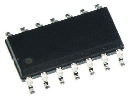
| 描述 | IC OPAMP AUDIO 35MHZ RRO 14SOIC音频放大器 Hi-Perf,Bipolar-Inp Audio Op Amp |
| 产品分类 | Linear - Amplifiers - Instrumentation, OP Amps, Buffer Amps集成电路 - IC |
| 品牌 | Texas Instruments |
| 产品手册 | http://www.ti.com/litv/sbos474b |
| 产品图片 |
|
| rohs | 符合RoHS无铅 / 符合限制有害物质指令(RoHS)规范要求 |
| 产品系列 | 音频 IC,音频放大器,Texas Instruments OPA1604AIDSoundPlus™ |
| 数据手册 | |
| 产品型号 | OPA1604AID |
| PCN设计/规格 | |
| THD+噪声 | 0.00003 % |
| 产品 | General Purpose Audio Amplifiers |
| 产品种类 | 音频放大器 |
| 供应商器件封装 | 14-SOIC |
| 共模抑制比—最小值 | 114 dB |
| 其它名称 | 296-33469-5 |
| 包装 | 管件 |
| 压摆率 | 20 V/µs |
| 商标 | Texas Instruments |
| 增益带宽生成 | 35 MHz |
| 增益带宽积 | 35MHz |
| 安装类型 | 表面贴装 |
| 安装风格 | SMD/SMT |
| 封装 | Tube |
| 封装/外壳 | 14-SOIC(0.154",3.90mm 宽) |
| 封装/箱体 | SOIC-14 |
| 工作温度 | -40°C ~ 85°C |
| 工作电源电压 | 4.5 V to 36 V |
| 工厂包装数量 | 50 |
| 放大器类型 | 音频 |
| 最大工作温度 | + 85 C |
| 最小工作温度 | - 40 C |
| 标准包装 | 50 |
| 电压-电源,单/双 (±) | 4.5 V ~ 36 V, ±2.25 V ~ 18 V |
| 电压-输入失调 | 100µV |
| 电流-电源 | 2.6mA |
| 电流-输入偏置 | 20nA |
| 电流-输出/通道 | 30mA |
| 电源电流 | 2.8 mA |
| 电路数 | 4 |
| 类型 | 4-Channel Rail-to-Rail |
| 系列 | OPA1604 |
| 设计资源 | http://www.digikey.com/product-highlights/cn/zh/texas-instruments-webench-design-center/3176 |
| 输入补偿电压 | 1 mV |
| 输出功率 | - |
| 输出类型 | 满摆幅 |


- 商务部:美国ITC正式对集成电路等产品启动337调查
- 曝三星4nm工艺存在良率问题 高通将骁龙8 Gen1或转产台积电
- 太阳诱电将投资9.5亿元在常州建新厂生产MLCC 预计2023年完工
- 英特尔发布欧洲新工厂建设计划 深化IDM 2.0 战略
- 台积电先进制程称霸业界 有大客户加持明年业绩稳了
- 达到5530亿美元!SIA预计今年全球半导体销售额将创下新高
- 英特尔拟将自动驾驶子公司Mobileye上市 估值或超500亿美元
- 三星加码芯片和SET,合并消费电子和移动部门,撤换高东真等 CEO
- 三星电子宣布重大人事变动 还合并消费电子和移动部门
- 海关总署:前11个月进口集成电路产品价值2.52万亿元 增长14.8%


PDF Datasheet 数据手册内容提取
OPA1602 OPA1604 Burr-Brown Audio www.ti.com SBOS474B–APRIL2011–REVISEDNOVEMBER2011 ™ High-Performance, Bipolar-Input AUDIO OPERATIONAL AMPLIFIERS CheckforSamples:OPA1602,OPA1604 FEATURES DESCRIPTION 1 • SUPERIORSOUNDQUALITY The OPA1602 and OPA1604 bipolar-input 234 operational amplifiers achieve very low 2.5nV/√Hz • ULTRALOWNOISE:2.5nV/√Hzat1kHz noise density with an ultralow distortion of 0.00003% • ULTRALOWDISTORTION:0.00003%at1kHz at 1kHz. The OPA1602 and OPA1604 series of op • HIGHSLEWRATE:20V/μs amps offer rail-to-rail output swing to within 600mV with 2kΩ load, which increases headroom and • WIDEBANDWIDTH:35MHz(G=+1) maximizes dynamic range. These devices also have • HIGHOPEN-LOOPGAIN:120dB ahighoutputdrivecapabilityof±30mA. • UNITYGAINSTABLE These devices operate over a very wide supply range • LOWQUIESCENTCURRENT: of ±2.25V to ±18V, on only 2.6mA of supply current 2.6mAPERCHANNEL per channel. The OPA1602 and OPA1604 are • RAIL-TO-RAILOUTPUT unity-gain stable and provide excellent dynamic behavioroverawiderangeofloadconditions. • WIDESUPPLYRANGE:±2.25Vto ±18V These devices also feature completely independent • DUALANDQUADVERSIONSAVAILABLE circuitry for lowest crosstalk and freedom from interactions between channels, even when overdriven APPLICATIONS oroverloaded. • PROFESSIONALAUDIOEQUIPMENT The OPA1602 and OPA1604 are specified • BROADCASTSTUDIOEQUIPMENT from–40°Cto+85°C.SoundPlus™ • ANALOGANDDIGITALMIXERS • HIGH-ENDA/VRECEIVERS • HIGH-ENDBLU-RAY™PLAYERS V+ Pre-Output Driver OUT IN- IN+ V- 1 Pleasebeawarethatanimportantnoticeconcerningavailability,standardwarranty,anduseincriticalapplicationsofTexas Instrumentssemiconductorproductsanddisclaimerstheretoappearsattheendofthisdatasheet. SoundPlusisatrademarkofTexasInstrumentsIncorporated. 2 BLU-RAYisatrademarkofBlu-rayDiscAssociation. 3 Allothertrademarksarethepropertyoftheirrespectiveowners. 4 PRODUCTIONDATAinformationiscurrentasofpublicationdate. Copyright©2011,TexasInstrumentsIncorporated Products conform to specifications per the terms of the Texas Instruments standard warranty. Production processing does not necessarilyincludetestingofallparameters.
OPA1602 OPA1604 SBOS474B–APRIL2011–REVISEDNOVEMBER2011 www.ti.com This integrated circuit can be damaged by ESD. Texas Instruments recommends that all integrated circuits be handled with appropriateprecautions.Failuretoobserveproperhandlingandinstallationprocedurescancausedamage. ESDdamagecanrangefromsubtleperformancedegradationtocompletedevicefailure.Precisionintegratedcircuitsmaybemore susceptibletodamagebecauseverysmallparametricchangescouldcausethedevicenottomeetitspublishedspecifications. ABSOLUTE MAXIMUM RATINGS(1) Overoperatingfree-airtemperaturerange(unlessotherwisenoted). VALUE UNIT SupplyVoltage V =(V+)–(V–) 40 V S InputVoltage (V–)–0.5to(V+)+0.5 V InputCurrent(Allpinsexceptpower-supplypins) ±10 mA OutputShort-Circuit(2) Continuous OperatingTemperature –55to+125 °C StorageTemperature –65to+150 °C JunctionTemperature 200 °C HumanBodyModel(HBM) 4 kV ESDRatings ChargedDeviceModel(CDM) 1 kV MachineModel(MM) 200 V (1) Stressesabovetheseratingsmaycausepermanentdamage.Exposuretoabsolutemaximumconditionsforextendedperiodsmay degradedevicereliability.Thesearestressratingsonly,andfunctionaloperationofthedeviceattheseoranyotherconditionsbeyond thosespecifiedisnotsupported. (2) Short-circuittoV /2(groundinsymmetricaldualsupplysetups),oneamplifierperpackage. S PACKAGEINFORMATION(1) PRODUCT PACKAGE-LEAD PACKAGEDESIGNATOR PACKAGEMARKING SO-8 D O1602A OPA1602 MSOP-8 DGK OCKQ SO-14 D O1604A OPA1604 TSSOP-14 PW O1604A (1) ForthemostcurrentpackageandorderinginformationseethePackageOptionAddendumattheendofthisdocument,orseetheTI websiteatwww.ti.com. PIN CONFIGURATIONS OPA1602 SO-8,MSOP-8 OPA1604 (TOPVIEW) SO-14,TSSOP-14 (TOPVIEW) OUT A 1 8 V+ Out A 1 14 Out D -IN A 2 A 7 OUT B -In A 2 13 -In D +IN A 3 B 6 -IN B A D +In A 3 12 +In D V- 4 5 +IN B V+ 4 11 V- + In B 5 10 + In C B C -In B 6 9 -In C Out B 7 8 Out C 2 Copyright©2011,TexasInstrumentsIncorporated ProductFolderLink(s):OPA1602OPA1604
OPA1602 OPA1604 www.ti.com SBOS474B–APRIL2011–REVISEDNOVEMBER2011 ELECTRICAL CHARACTERISTICS: V = ±2.25V to ±18V S AtT =+25°CandR =2kΩ,unlessotherwisenoted.V =V =midsupply,unlessotherwisenoted. A L CM OUT OPA1602,OPA1604 PARAMETER CONDITIONS MIN TYP MAX UNIT AUDIOPERFORMANCE TotalHarmonicDistortion+Noise THD+N 0.00003 % G=+1,f=1kHz,VO=3VRMS –130 dB IntermodulationDistortion IMD G=+1,VO=3VRMS 0.00003 % SMPTE/DINTwo-Tone,4:1(60Hzand7kHz) –130 dB DIM30 0.00003 % (3kHzsquarewaveand15kHzsinewave) –130 dB 0.00003 % CCIFTwin-Tone(19kHzand20kHz) –130 dB FREQUENCYRESPONSE Gain-BandwidthProduct GBW G=+1 35 MHz SlewRate SR G=–1 20 V/μs FullPowerBandwidth(1) VO=1VP 3 MHz OverloadRecoveryTime G=–10 1 μs NOISE InputVoltageNoise f=20Hzto20kHz 2.5 μVPP InputVoltageNoiseDensity en f=100Hz 2.5 nV/√Hz f=1kHz 2.5 nV/√Hz InputCurrentNoiseDensity In f=100Hz 2.2 pA/√Hz f=1kHz 1.8 pA/√Hz OFFSETVOLTAGE InputOffsetVoltage VOS VS=±15V ±0.1 ±1 mV vsPowerSupply PSRR VS=±2.25Vto±18V 0.5 2 μV/V ChannelSeparation(DualandQuad) f=1kHz -130 dB INPUTBIASCURRENT InputBiasCurrent IB VCM=0V ±20 ±200 nA InputOffsetCurrent IOS VCM=0V ±20 ±200 nA INPUTVOLTAGERANGE Common-ModeVoltageRange VCM (V–)+2 (V+)–2 V Common-ModeRejectionRatio CMRR (V–)+2V≤VCM≤(V+)–2V,VS≥±5V 114 120 dB (V–)+2V≤VCM≤(V+)–2V,VS<±5V 100 110 dB INPUTIMPEDANCE Differential 20k||2 Ω||pF Common-Mode 109||2.5 Ω||pF OPEN-LOOPGAIN Open-LoopVoltageGain AOL (V–)+0.6V≤VO≤(V+)–0.6V,RL=2kΩ,VS≥±5V 114 120 dB (V–)+0.6V≤VO≤(V+)–0.6V,RL=2kΩ,VS<±5V 106 114 dB OUTPUT VoltageOutput VOUT RL=2kΩ,AOL≥114dB,VS≥±5V (V–)+0.6 (V+)–0.6 V RL=2kΩ,AOL≥106dB,VS<±5V (V–)+0.6 (V+)–0.6 V OutputCurrent IOUT SeeTypicalCharacteristics mA Open-LoopOutputImpedance ZO f=1MHz 25 Ω Short-CircuitCurrent(2) ISC +70/–60 mA CapacitiveLoadDrive CLOAD SeeTypicalCharacteristics pF (1) Full-powerbandwidth=SR/(2π×V ),whereSR=slewrate. P (2) Onechannelatatime. Copyright©2011,TexasInstrumentsIncorporated 3 ProductFolderLink(s):OPA1602OPA1604
OPA1602 OPA1604 SBOS474B–APRIL2011–REVISEDNOVEMBER2011 www.ti.com ELECTRICAL CHARACTERISTICS: V = ±2.25V to ±18V (continued) S AtT =+25°CandR =2kΩ,unlessotherwisenoted.V =V =midsupply,unlessotherwisenoted. A L CM OUT OPA1602,OPA1604 PARAMETER CONDITIONS MIN TYP MAX UNIT POWERSUPPLY SpecifiedVoltage VS ±2.25 ±18 V QuiescentCurrent(3) xxDual,perchannel IQ IOUT=0A 2.6 3.2 mA Quad,perchannel IQ IOUT=0A 2.8 3.4 mA TEMPERATURERANGE SpecifiedRange –40 +85 °C OperatingRange –55 +125 °C (3) I valueisbasedonflashtest. Q THERMAL INFORMATION: OPA1602 OPA1602 OPA1602 THERMALMETRIC(1) D DGK UNITS 8PINS 8PINS θ Junction-to-ambientthermalresistance 105.4 154.7 JA θ Junction-to-case(top)thermalresistance 58.6 49.7 JCtop θ Junction-to-boardthermalresistance 64.2 107.9 JB °C/W ψ Junction-to-topcharacterizationparameter 14.1 2.5 JT ψ Junction-to-boardcharacterizationparameter 66.5 106.7 JB θ Junction-to-case(bottom)thermalresistance N/A N/A JCbot (1) Formoreinformationabouttraditionalandnewthermalmetrics,seetheICPackageThermalMetricsapplicationreport,SPRA953. THERMAL INFORMATION: OPA1604 OPA1604 OPA1604 THERMALMETRIC(1) D PW UNITS 14PINS 14PINS θ Junction-to-ambientthermalresistance 92.8 122.5 JA θ Junction-to-case(top)thermalresistance 44.4 36.5 JCtop θ Junction-to-boardthermalresistance 39.6 53.9 JB °C/W ψ Junction-to-topcharacterizationparameter 10.4 2.5 JT ψ Junction-to-boardcharacterizationparameter 39.3 53.2 JB θ Junction-to-case(bottom)thermalresistance N/A N/A JCbot (1) Formoreinformationabouttraditionalandnewthermalmetrics,seetheICPackageThermalMetricsapplicationreport,SPRA953. 4 Copyright©2011,TexasInstrumentsIncorporated ProductFolderLink(s):OPA1602OPA1604
OPA1602 OPA1604 www.ti.com SBOS474B–APRIL2011–REVISEDNOVEMBER2011 TYPICAL CHARACTERISTICS AtT =+25°C,V =±15V,andR =2kΩ,unlessotherwisenoted. A S L INPUTVOLTAGENOISEDENSITYAND INPUTCURRENTNOISEDENSITYvsFREQUENCY 0.1HzTO10HzNOISE 100 )zHz) H? ?V/pA/ y (nse ( oise DensitCurrent Noi 10 VoltDaegnes Nityoise 50nV/div e Nas Voltagnput Bi CurDreennts Nityoise I 1 0.1 1 10 100 1k 10k 100k Time (1s/div) Frequency (Hz) Figure1. Figure2. VOLTAGENOISEvsSOURCERESISTANCE MAXIMUMOUTPUTVOLTAGEvsFREQUENCY )Hz 10k 15 ÖV/ VS=±15V Maximum output n 12.5 voltage without slew- (O EO OPA160x rate induced distortion al Density, E 1010k RS Voltage (V)P 71.05 ctr ut e Spe OPA164x Outp 5 VS=±5V s 10 Noi 2.5 VS=±2.25V e Resistor oltag 1 Noise EO2= en2+ (inRS)2+ 4kTRS 0 V 10k 100k 1M 10M 100 1k 10k 100k 1M Source Resistance, R (W) Frequency (Hz) S Figure3. Figure4. GAINANDPHASEvsFREQUENCY CLOSED-LOOPGAINvsFREQUENCY 140 180 25 20 120 Gain G = +10 15 100 135 P 10 B) 80 has B) 5 G = +1 Gain (d 6400 90 e (degre Gain (d -05 e Phase s) -10 20 45 G =-1 -15 0 -20 -20 0 -25 10 100 1k 10k 100k 1M 10M 100M 100k 1M 10M 100M Frequency (Hz) Frequency (Hz) Figure5. Figure6. Copyright©2011,TexasInstrumentsIncorporated 5 ProductFolderLink(s):OPA1602OPA1604
OPA1602 OPA1604 SBOS474B–APRIL2011–REVISEDNOVEMBER2011 www.ti.com TYPICAL CHARACTERISTICS (continued) AtT =+25°C,V =±15V,andR =2kΩ,unlessotherwisenoted. A S L THD+NRATIOvsFREQUENCY THD+NRATIOvsFREQUENCY 0.001 -100 0.01 -80 onic Distortion + Noise (%) 0.0001 GGG ===R -++L111=,,, R6RR0LLL0===W 66200kW00WW GGG === -++111,00 R,, RRLLL= ==2 k62W0kW0W -120 Total Harmonic Distortion + onic Distortion + Noise (%) 0.00.000011 RSOURCEOP+-A111556VV02 RL RRRRSSSS==== 0361W00kW00WW --110200 Total Harmonic Distortion + m N m N Total Har 0.00001 VBWOU T== 8 03kVHRMzS RL= 2kW -140 oise (dB) Total Har 0.00001 VOUT= 3VRMS,BW = 80kHz -140 oise (dB) 10 100 1k 10k 20k 10 100 1k 10k 20k Frequency (Hz) Frequency (Hz) Figure7. Figure8. THD+NRATIOvsFREQUENCY THD+NRATIOvsFREQUENCY 0.01 -80 0.01 -80 onic Distortion + Noise (%) 0.00.000011 GGG === -++111,,, RRRLLL=== 66200kW00WW RL=GGG 6 ===0 0-++W111,00 R,, RRLLL= ==2 k62W0kW0W --110200 Total Harmonic Distortion + onic Distortion + Noise (%) 0.00.000011 RSOURCEOP+-A111556VV02 RL RRRRSSSS==== 036100kWW00WW --110200 Total Harmonic Distortion + m N m N Total Har 0.00001 VBWOU T>= 5 030VkRHMzS RL= 2kW -140 oise (dB) Total Har 0.00001 VBWOU T>= 5 030VkRHMzS -140 oise (dB) 10 100 1k 10k 100k 10 100 1k 10k 100k Frequency (Hz) Frequency (Hz) Figure9. Figure10. INTERMODULATIONDISTORTIONvs THD+NRATIOvsOUTPUTAMPLITUDE OUTPUTAMPLITUDE 0.01 -80 0.1 -60 Total Harmonic Distortion + Noise (%) 0.00.000.000000111 1BRkWSHO Uz=R S8Ci0Egkn=Ha 0zlW RLGGGGGG= ======2 k--++++W111111,,,,00 RRRR,, RRRLLLLLLL===== == 6262 60k0k62WW0000kW0W0WWW ---111024000 Total Harmonic Distortion (dB) Intermodulation Distortion (%) 0.00.000.0000.00000.0000011111 GC(1 C9=D(13Ik 5FI+HkMk 1HTzH3w zza0 i snnsqd-iTnu o2ean0 rweekH awvzae)v)e, ST(6wM0oHP-TTzo Ean/neDd,I N47:k1Hz) -----81111002460000 Total Harmonic Distortion + Noise (dB) 0.1 1 10 20 0.1 1 10 20 Output Amplitude (VRMS) Output Amplitude (VRMS) Figure11. Figure12. 6 Copyright©2011,TexasInstrumentsIncorporated ProductFolderLink(s):OPA1602OPA1604
OPA1602 OPA1604 www.ti.com SBOS474B–APRIL2011–REVISEDNOVEMBER2011 TYPICAL CHARACTERISTICS (continued) AtT =+25°C,V =±15V,andR =2kΩ,unlessotherwisenoted. A S L CHANNELSEPARATIONvsFREQUENCY CMRRANDPSRRvsFREQUENCY(ReferredtoInput) -100 140 -105 VO= 3VRMS B) CMRR n (dB) --111105 G = +1 n Ratio (d 112000 -PSRR paratio --112205 RL= 600W ejectio 80 e R Channel S ----111133440505 RRLL== 52kkWW ommon-Mode 642000 +PSRR C -150 0 10 100 1k 10k 100k 1 10 100 1k 10k 100k 1M 10M 100M Frequency (Hz) Frequency (Hz) Figure13. Figure14. SMALL-SIGNALSTEPRESPONSE SMALL-SIGNALSTEPRESPONSE (100mV) (100mV) G = +1 G =-1 C = 50pF C = 50pF L L V/div +15V V/div RF=2kW m m 20 OPA1602 20 RI=2kW +15V OPA1602 -15V RL CL CL -15V Time (0.1ms/div) Time (0.1ms/div) Figure15. Figure16. LARGE-SIGNALSTEPRESPONSE LARGE-SIGNALSTEPRESPONSE G = +1 G =-1 C = 50pF C = 50pF L L R = 0W F v v di di V/ V/ 2 2 R = 100W F SeeApplication Information, Input Protectionsection Time (1ms/div) Time (1ms/div) Figure17. Figure18. Copyright©2011,TexasInstrumentsIncorporated 7 ProductFolderLink(s):OPA1602OPA1604
OPA1602 OPA1604 SBOS474B–APRIL2011–REVISEDNOVEMBER2011 www.ti.com TYPICAL CHARACTERISTICS (continued) AtT =+25°C,V =±15V,andR =2kΩ,unlessotherwisenoted. A S L SMALL-SIGNALOVERSHOOT SMALL-SIGNALOVERSHOOT vsCAPACITIVELOAD(100mVOutputStep) vsCAPACITIVELOAD(100mVOutputStep) 50 50 G = +1 G =-1 R = 0W +15V RS= 0W RI=2kW RF= 2kW S 40 RS 40 +15V OPA1602 RS ot (%) 30 -15V RL CL ot (%) 30 RS= 25W OP-A1156V02 CL ersho 20 RS= 25W ersho 20 Ov Ov R = 50W S 10 10 R = 50W S 0 0 0 100 200 300 400 500 600 0 100 200 300 400 500 600 700 800 900 1000 Capacitive Load (pF) Capacitive Load (pF) Figure19. Figure20. SMALL-SIGNALOVERSHOOT vsFEEDBACKCAPACITOR(100mVOutputStep) OPEN-LOOPGAINvsTEMPERATURE 50 2 R = 2kW CF L 40 RI=2kW RF= 2kW 1.5 +15V ot (%) 30 OPA1602 RS CL V/V) versho 20 -15V A(mOL 1 O G =-1 10 RI= RF= 2kW 0.5 R = 0W S C = 100pF L 0 0 0 0.5 1 1.5 2 2.5 3 3.5 4 -40 -15 10 35 60 85 Feedback Capacitor,C (pF) Temperature (°C) F Figure21. Figure22. I ANDI vsTEMPERATURE I ANDI vsCOMMON-MODEVOLTAGE B OS B OS 10 40 Average of 60 Units VS=±18V 5 30 -I OS A) 0 20 Common-Mode Range n and ICurrent (BOS---112-0505 -IB Iand I(nA)BOS --1120000 IOS -IB I -25 -30 -30 +IB -40 +IB -50 -25 0 25 50 75 100 125 -18 -14 -10 -6 -2 2 6 10 14 18 Temperature (°C) Common-Mode Voltage (V) Figure23. Figure24. 8 Copyright©2011,TexasInstrumentsIncorporated ProductFolderLink(s):OPA1602OPA1604
OPA1602 OPA1604 www.ti.com SBOS474B–APRIL2011–REVISEDNOVEMBER2011 TYPICAL CHARACTERISTICS (continued) AtT =+25°C,V =±15V,andR =2kΩ,unlessotherwisenoted. A S L QUIESCENTCURRENTvsTEMPERATURE QUIESCENTCURRENTvsSUPPLYVOLTAGE 4 3 2.9 OPA1604 3.5 2.8 OPA1604 2.7 3 2.6 A) A) m m 2.5 (Q (Q I 2.5 I 2.4 OPA1602 OPA1602 2.3 2 2.2 2.1 <−−−−−− Specified Temperature Range −−−−−−> <−−−−−− Specified Supply−Voltage Range −−−−−> 1.5 2 −40 −15 10 35 60 85 110 0 4 8 12 16 20 24 28 32 36 Temperature (°C) Supply Voltage (V) G017 G018 Figure25. Figure26. I WARMUP Q (DifferencefromI atStartup,PerChannel) SHORT-CIRCUITCURRENTvsTEMPERATURE Q 0.3 75 +I V =±18V SC S 70 0.25 65 A) OPA1604 m Channel ( 0.01.52 OPA1602 (mA)C 655050 -ISC er IS , pQ 0.1 45 DI 40 0.05 35 0 30 0 60 120 180 240 300 360 -50 -25 0 25 50 75 100 125 Time (s) Temperature (°C) Figure27. Figure28. OPEN-LOOPOUTPUTIMPEDANCEvs OUTPUTVOLTAGEvsOUTPUTCURRENT FREQUENCY 18 10k 16 V =±18V g (V) 14 S 1k n 12 +125°C Swi +85°C e 10 +25°C W) g ( 100 Volta -10 0-2°C5°C ZO ut -12 -40°C p Out -14 10 -16 -18 1 20 30 40 50 60 70 80 10 100 1k 10k 100k 1M 10M 100M Output Current (mA) Frequency (Hz) Figure29. Figure30. Copyright©2011,TexasInstrumentsIncorporated 9 ProductFolderLink(s):OPA1602OPA1604
OPA1602 OPA1604 SBOS474B–APRIL2011–REVISEDNOVEMBER2011 www.ti.com APPLICATION INFORMATION applications do not require equal positive and The OPA1602 and OPA1604 are unity-gain stable, negative output voltage swing. With the OPA160x precision dual and quad op amps with very low noise. series, power-supply voltages do not need to be Applications with noisy or high-impedance power equal. For example, the positive supply could be set supplies require decoupling capacitors close to the to+25Vwiththenegativesupplyat–5V. device pins. In most cases, 0.1μF capacitors are adequate. Figure 31 shows a simplified schematic of In all cases, the common-mode voltage must be theOPA160x(onechannelshown). maintained within the specified range. In addition, key parameters are assured over the specified OPERATING VOLTAGE temperature range of T = –40°C to +85°C. A Parameters that vary significantly with operating The OPA160x series op amps operate from ±2.25V voltage or temperature are shown in the Typical to ±18V supplies while maintaining excellent Characteristics. performance. The OPA160x series can operate with as little as +4.5V between the supplies and with up to +36V between the supplies. However, some V+ Pre-Output Driver OUT IN- IN+ V- Figure31. OPA160xSimplifiedSchematic 10 Copyright©2011,TexasInstrumentsIncorporated ProductFolderLink(s):OPA1602OPA1604
OPA1602 OPA1604 www.ti.com SBOS474B–APRIL2011–REVISEDNOVEMBER2011 INPUT PROTECTION The equation in Figure 33 shows the calculation of thetotalcircuitnoise,withtheseparameters: The input terminals of the OPA1602 and OPA1604 • e =Voltagenoise are protected from excessive differential voltage with n back-to-back diodes, as Figure 32 illustrates. In most • i =Currentnoise n circuit applications, the input protection circuitry has • R =Sourceimpedance S no consequence. However, in low-gain or G = +1 • k=Boltzmann’sconstant=1.38×10⁻²³J/K circuits, fast ramping input signals can forward bias • T=TemperatureindegreesKelvin(K) these diodes because the output of the amplifier cannot respond rapidly enough to the input ramp. This effect is illustrated in Figure 17 of the Typical )Hz 10k Ö Characteristics. If the input signal is fast enough to V/ n create this forward bias condition, the input signal (O EO OPA160x E 1k csuigrnreanltcumrruesnttbisenliomtitinehdetroen1tl0ymliAmioterdl,eassn.inIfptuhteseinrpieust nsity, RS e resistor (RI) and/or a feedback resistor (RF) can be al D 100 used to limit the signal input current. This resistor ctr e degrades the low-noise performance of the OPA160x p S and is examined in the following Noise Performance se 10 OPA164x section. Figure 32 shows an example configuration Noi warheeunsbeodt.h current-limiting input and feeback resistors oltage 1 RNeosiissteor EO2= en2+ (inRS)2+ 4kTRS V 100 1k 10k 100k 1M Source Resistance, R (W) R S F Figure33. NoisePerformanceoftheOPA160xin Unity-GainBufferConfiguration - BASIC NOISE CALCULATIONS OPA160x Output R Design of low-noise op amp circuits requires careful I + Input consideration of a variety of possible noise contributors: noise from the signal source, noise generated in the op amp, and noise from the feedback network resistors. The total noise of the Figure32. PulsedOperation circuit is the root-sum-square combination of all noise components. The resistive portion of the source impedance NOISE PERFORMANCE produces thermal noise proportional to the square Figure 33 shows the total circuit noise for varying root of the resistance. Figure 33 plots this equation. source impedances with the op amp in a unity-gain The source impedance is usually fixed; consequently, configuration (no feedback resistor network, and select the op amp and the feedback resistors to thereforenoadditionalnoisecontributions). minimize the respective contributions to the total noise. TheOPA160x(GBW=35MHz,G=+1)isshownwith total circuit noise calculated. The op amp itself Figure 34 illustrates both inverting and noninverting contributes both a voltage noise component and a op amp circuit configurations with gain. In circuit current noise component. The voltage noise is configurations with gain, the feedback network commonly modeled as a time-varying component of resistors also contribute noise. The current noise of the offset voltage. The current noise is modeled as the op amp reacts with the feedback resistors to the time-varying component of the input bias current create additional noise components. The feedback and reacts with the source resistance to create a resistor values can generally be chosen to make voltage component of noise. Therefore, the lowest these noise sources negligible. The equations for noise op amp for a given application depends on the totalnoiseareshownforbothconfigurations. source impedance. For low source impedance, current noise is negligible, and voltage noise generally dominates. The low voltage noise of the OPA160x series op amps makes them a better choiceforlowsourceimpedancesoflessthan1kΩ. Copyright©2011,TexasInstrumentsIncorporated 11 ProductFolderLink(s):OPA1602OPA1604
OPA1602 OPA1604 SBOS474B–APRIL2011–REVISEDNOVEMBER2011 www.ti.com A) Noise in Noninverting Gain Configuration Noise at the output: R 2 2 2 2 R R R R E 2= 1 + 2 e 2+ 2 e 2+ e 2+ 1 + 2 e2 1 O R n R 1 2 R s 1 1 1 E O Where e = 4kTR = thermal noise of R R S S S S e = 4kTR = thermal noise of R 1 1 1 V S e = 4kTR = thermal noise of R 2 2 2 B) Noise in Inverting Gain Configuration Noise at the output: R 2 2 2 2 R R R E 2= 1 + 2 e 2+ 2 e 2+ e 2+ 2 e2 R1 O R1+ RS n R1+ RS 1 2 R1+ RS s E R O S Where e = 4kTR = thermal noise of R S S S V S e = 4kTR = thermal noise of R 1 1 1 e = 4kTR = thermal noise of R 2 2 2 Note: FortheOPA160xseriesofopampsat1kHz,e =2.5nV/√Hzandi =1.8pA√Hz. n n Figure34. NoiseCalculationinGainConfigurations 12 Copyright©2011,TexasInstrumentsIncorporated ProductFolderLink(s):OPA1602OPA1604
OPA1602 OPA1604 www.ti.com SBOS474B–APRIL2011–REVISEDNOVEMBER2011 TOTAL HARMONIC DISTORTION The validity of this technique can be verified by MEASUREMENTS duplicating measurements at high gain and/or high frequency where the distortion is within the The OPA160x series op amps have excellent measurement capability of the test equipment. distortion characteristics. THD + noise is below Measurements for this data sheet were made with an 0.00008% (G = +1, V = 3V , BW = 80kHz) O RMS Audio Precision System Two distortion/noise throughout the audio frequency range, 20Hz to analyzer, which greatly simplifies such repetitive 20kHz, with a 2kΩ load (see Figure 7 for measurements. The measurement technique can, characteristicperformance). however, be performed with manual distortion The distortion produced by the OPA160x series op measurementinstruments. amps is below the measurement limit of many commercially available distortion analyzers. However, CAPACITIVE LOADS a special test circuit (such as Figure 35 shows) can The dynamic characteristics of the OPA1602 and beusedtoextendthemeasurementcapabilities. OPA1604 have been optimized for commonly Op amp distortion can be considered an internal error encountered gains, loads, and operating conditions. source that can be referred to the input. Figure 35 The combination of low closed-loop gain and high shows a circuit that causes the op amp distortion to capacitive loads decreases the phase margin of the be gained up (refer to the table in Figure 35 for the amplifier and can lead to gain peaking or oscillations. distortion gain factor for various signal gains). The As a result, heavier capacitive loads must be isolated addition of R to the otherwise standard noninverting from the output. The simplest way to achieve this 3 amplifier configuration alters the feedback factor or isolation is to add a small resistor (R equal to 50Ω, S noise gain of the circuit. The closed-loop gain is forexample)inserieswiththeoutput. unchanged, but the feedback available for error This small series resistor also prevents excess power correction is reduced by the distortion gain factor, dissipation if the output of the device becomes thus extending the resolution by the same amount. shorted. Figure 19 illustrates a graph of Small-Signal Note that the input signal and load applied to the op Overshoot vs Capacitive Load for several values of amp are the same as with conventional feedback R . Also, refer to Applications Bulletin AB-028 without R . The value of R should be kept small to S 3 3 (literature number SBOA015, available for download minimizeitseffectonthedistortionmeasurements. from the TI web site) for details of analysis techniquesandapplicationcircuits. R R 1 2 SIGNAL DISTORTION GAIN GAIN R1 R2 R3 +1 101 ¥ 1kW 10W R R3 OPA160x VO= 3VRMS -1 101 4.99kW 4.99kW 49.9W Signal Gain = 1+ 2 R1 +10 110 549W 4.99kW 49.9W R Distortion Gain = 1+ 2 R II R 1 3 Generator Analyzer Output Input Audio Precision System Two(1) Load with PC Controller (1) Formeasurementbandwidth,seeFigure7throughFigure12. Figure35. DistortionTestCircuit Copyright©2011,TexasInstrumentsIncorporated 13 ProductFolderLink(s):OPA1602OPA1604
OPA1602 OPA1604 SBOS474B–APRIL2011–REVISEDNOVEMBER2011 www.ti.com POWER DISSIPATION When the operational amplifier connects into a circuit such as that illustrated in Figure 36, the ESD The OPA1602 and OPA1604 series op amps are protection components are intended to remain capable of driving 2kΩ loads with a power-supply inactive and not become involved in the application voltage up to ±18V and full operating temperature circuit operation. However, circumstances may arise range. Internal power dissipation increases when where an applied voltage exceeds the operating operating at high supply voltages. Copper leadframe voltage range of a given pin. Should this condition construction used in the OPA160x series op amps occur, there is a risk that some of the internal ESD improves heat dissipation compared to conventional protection circuits may be biased on, and conduct materials. Circuit board layout can also help minimize current. Any such current flow occurs through junction temperature rise. Wide copper traces help steering diode paths and rarely involves the dissipate the heat by acting as an additional heat absorptiondevice. sink. Temperature rise can be further minimized by soldering the devices to the circuit board rather than Figure 36 depicts a specific example where the input usingasocket. voltage, V , exceeds the positive supply voltage IN (+V ) by 500mV or more. Much of what happens in S ELECTRICAL OVERSTRESS the circuit depends on the supply characteristics. If +V can sink the current, one of the upper input Designers often ask questions about the capability of S steering diodes conducts and directs current to +V . an operational amplifier to withstand electrical S Excessively high current levels can flow with overstress. These questions tend to focus on the increasingly higher V . As a result, the datasheet deviceinputs,butmayinvolvethesupplyvoltagepins IN specifications recommend that applications limit the or even the output pin. Each of these different pin inputcurrentto10mA. functions have electrical stress limits determined by the voltage breakdown characteristics of the If the supply is not capable of sinking the current, V IN particular semiconductor fabrication process and may begin sourcing current to the operational specific circuits connected to the pin. Additionally, amplifier, and then take over as the source of positive internal electrostatic discharge (ESD) protection is supply voltage. The danger in this case is that the built into these circuits to protect them from voltage can rise to levels that exceed the operational accidental ESD events both before and during amplifier absolute maximum ratings. In extreme but productassembly. rare cases, the absorption device triggers on while +V and –V are applied. If this event happens, a It is helpful to have a good understanding of this S S direct current path is established between the +V basic ESD circuitry and its relevance to an electrical S and –V supplies. The power dissipation of the overstress event. Figure 36 illustrates the ESD S absorption device is quickly exceeded, and the circuits contained in the OPA160x (indicated by the extreme internal heating destroys the operational dashed line area). The ESD protection circuitry amplifier. involves several current-steering diodes connected from the input and output pins and routed back to the Another common question involves what happens to internal power-supply lines, where they meet at an the amplifier if an input signal is applied to the input absorption device internal to the operational amplifier. while the power supplies +V and/or –V are at 0V. S S This protection circuitry is intended to remain inactive Again,itdependsonthesupplycharacteristicwhileat duringnormalcircuitoperation. 0V, or at a level below the input signal amplitude. If the supplies appear as high impedance, then the An ESD event produces a short duration, operational amplifier supply current may be supplied high-voltage pulse that is transformed into a short by the input source via the current steering diodes. duration, high-current pulse as it discharges through This state is not a normal bias condition; the amplifier a semiconductor device. The ESD protection circuits most likely will not operate normally. If the supplies are designed to provide a current path around the are low impedance, then the current through the operational amplifier core to prevent it from being steering diodes can become quite high. The current damaged. The energy absorbed by the protection level depends on the ability of the input source to circuitryisthendissipatedasheat. delivercurrent,andanyresistanceintheinputpath. When an ESD voltage develops across two or more of the amplifier device pins, current flows through one or more of the steering diodes. Depending on the path that the current takes, the absorption device may activate. The absorption device internal to the OPA160x triggers when a fast ESD voltage pulse is impressed across the supply pins. Once triggered, it quickly activates, clamping the ESD pulse to a safe voltagelevel. 14 Copyright©2011,TexasInstrumentsIncorporated ProductFolderLink(s):OPA1602OPA1604
OPA1602 OPA1604 www.ti.com SBOS474B–APRIL2011–REVISEDNOVEMBER2011 If there is an uncertainty about the ability of the The zener voltage must be selected such that the supply to absorb this current, external zener diodes diode does not turn on during normal operation. may be added to the supply pins as shown in However, its zener voltage should be low enough so Figure36. that the zener diode conducts if the supply pin begins toriseabovethesafeoperatingsupplyvoltagelevel. TVS R F +V S +V OPA160x R I -In ESD Current- Steering Diodes Op-Amp Out R S +In Core Edge-Triggered ESD R I Absorption Circuit L D VIN(1) -V -V S TVS (1) V =+V +500mV. IN S Figure36. EquivalentInternalESDCircuitryandItsRelationtoaTypicalCircuitApplication(Single ChannelShown) Copyright©2011,TexasInstrumentsIncorporated 15 ProductFolderLink(s):OPA1602OPA1604
OPA1602 OPA1604 SBOS474B–APRIL2011–REVISEDNOVEMBER2011 www.ti.com APPLICATION CIRCUIT AnadditionalapplicationideaisshowninFigure37. 820W 2200pF +V 0.1mF A (+15V) 330W I L+ OUT OPA160x 2700pF -VA 680W 620W (-15V) 0.1mF +VA 0.1mF (+15V) Audio DAC with Differential Current 100W Outputs 820W OPA160x L Ch Output 8200pF 2200pF -V A (-15V) +V 0.1mF 0.1mF A (+15V) 680W 620W I L- OUT OPA160x 330W 2700pF -V A (-15V) 0.1mF Figure37. AudioDACI/VConverterandOutputFilter 16 Copyright©2011,TexasInstrumentsIncorporated ProductFolderLink(s):OPA1602OPA1604
OPA1602 OPA1604 www.ti.com SBOS474B–APRIL2011–REVISEDNOVEMBER2011 REVISION HISTORY NOTE:Pagenumbersforpreviousrevisionsmaydifferfrompagenumbersinthecurrentversion. ChangesfromRevisionA(April,2011)toRevisionB Page • RevisedminimumandtypicalCommon-moderejectionratiospecifications ........................................................................ 3 • Addedfootnote(2)toElectricalCharacteristicstable........................................................................................................... 3 • Addedseparatequiescentcurrentspecificationsfordualandquadversions ..................................................................... 4 • Addedfootnote(3)toElectricalCharacteristicstable........................................................................................................... 4 • CorrectedproductidentificationandvaluesinOPA1602ThermalInformationtable ........................................................... 4 • AddedvaluestoOPA1604ThermalInformationtable. ........................................................................................................ 4 • UpdateddevicenameinFigure3......................................................................................................................................... 5 • UpdatedFigure25toshowbothdevices ............................................................................................................................. 9 • UpdatedFigure26toshowbothdevices ............................................................................................................................. 9 • UpdateddevicenameinFigure33..................................................................................................................................... 11 • ChangedPowerDissipationsection ................................................................................................................................... 14 Copyright©2011,TexasInstrumentsIncorporated 17 ProductFolderLink(s):OPA1602OPA1604
PACKAGE OPTION ADDENDUM www.ti.com 11-Apr-2013 PACKAGING INFORMATION Orderable Device Status Package Type Package Pins Package Eco Plan Lead/Ball Finish MSL Peak Temp Op Temp (°C) Top-Side Markings Samples (1) Drawing Qty (2) (3) (4) OPA1602AID ACTIVE SOIC D 8 75 Green (RoHS CU NIPDAU Level-2-260C-1 YEAR -40 to 85 01602A & no Sb/Br) OPA1602AIDGK ACTIVE VSSOP DGK 8 80 Green (RoHS CU NIPDAU Level-2-260C-1 YEAR -40 to 85 OCKQ & no Sb/Br) OPA1602AIDGKR ACTIVE VSSOP DGK 8 2500 Green (RoHS CU NIPDAU Level-2-260C-1 YEAR -40 to 85 OCKQ & no Sb/Br) OPA1602AIDR ACTIVE SOIC D 8 2500 Green (RoHS CU NIPDAU Level-2-260C-1 YEAR -40 to 85 01602A & no Sb/Br) OPA1604AID ACTIVE SOIC D 14 50 Green (RoHS CU NIPDAU Level-2-260C-1 YEAR -40 to 85 01604A & no Sb/Br) OPA1604AIDR ACTIVE SOIC D 14 2500 Green (RoHS CU NIPDAU Level-2-260C-1 YEAR -40 to 85 01604A & no Sb/Br) OPA1604AIPW ACTIVE TSSOP PW 14 90 Green (RoHS CU NIPDAU Level-2-260C-1 YEAR -40 to 85 OPA1604 & no Sb/Br) OPA1604AIPWR ACTIVE TSSOP PW 14 2000 Green (RoHS CU NIPDAU Level-2-260C-1 YEAR -40 to 85 OPA1604 & no Sb/Br) (1) The marketing status values are defined as follows: ACTIVE: Product device recommended for new designs. LIFEBUY: TI has announced that the device will be discontinued, and a lifetime-buy period is in effect. NRND: Not recommended for new designs. Device is in production to support existing customers, but TI does not recommend using this part in a new design. PREVIEW: Device has been announced but is not in production. Samples may or may not be available. OBSOLETE: TI has discontinued the production of the device. (2) Eco Plan - The planned eco-friendly classification: Pb-Free (RoHS), Pb-Free (RoHS Exempt), or Green (RoHS & no Sb/Br) - please check http://www.ti.com/productcontent for the latest availability information and additional product content details. TBD: The Pb-Free/Green conversion plan has not been defined. Pb-Free (RoHS): TI's terms "Lead-Free" or "Pb-Free" mean semiconductor products that are compatible with the current RoHS requirements for all 6 substances, including the requirement that lead not exceed 0.1% by weight in homogeneous materials. Where designed to be soldered at high temperatures, TI Pb-Free products are suitable for use in specified lead-free processes. Pb-Free (RoHS Exempt): This component has a RoHS exemption for either 1) lead-based flip-chip solder bumps used between the die and package, or 2) lead-based die adhesive used between the die and leadframe. The component is otherwise considered Pb-Free (RoHS compatible) as defined above. Green (RoHS & no Sb/Br): TI defines "Green" to mean Pb-Free (RoHS compatible), and free of Bromine (Br) and Antimony (Sb) based flame retardants (Br or Sb do not exceed 0.1% by weight in homogeneous material) (3) MSL, Peak Temp. -- The Moisture Sensitivity Level rating according to the JEDEC industry standard classifications, and peak solder temperature. Addendum-Page 1
PACKAGE OPTION ADDENDUM www.ti.com 11-Apr-2013 (4) Multiple Top-Side Markings will be inside parentheses. Only one Top-Side Marking contained in parentheses and separated by a "~" will appear on a device. If a line is indented then it is a continuation of the previous line and the two combined represent the entire Top-Side Marking for that device. Important Information and Disclaimer:The information provided on this page represents TI's knowledge and belief as of the date that it is provided. TI bases its knowledge and belief on information provided by third parties, and makes no representation or warranty as to the accuracy of such information. Efforts are underway to better integrate information from third parties. TI has taken and continues to take reasonable steps to provide representative and accurate information but may not have conducted destructive testing or chemical analysis on incoming materials and chemicals. TI and TI suppliers consider certain information to be proprietary, and thus CAS numbers and other limited information may not be available for release. In no event shall TI's liability arising out of such information exceed the total purchase price of the TI part(s) at issue in this document sold by TI to Customer on an annual basis. Addendum-Page 2
PACKAGE MATERIALS INFORMATION www.ti.com 20-Aug-2017 TAPE AND REEL INFORMATION *Alldimensionsarenominal Device Package Package Pins SPQ Reel Reel A0 B0 K0 P1 W Pin1 Type Drawing Diameter Width (mm) (mm) (mm) (mm) (mm) Quadrant (mm) W1(mm) OPA1602AIDGKR VSSOP DGK 8 2500 330.0 12.4 5.3 3.4 1.4 8.0 12.0 Q1 OPA1602AIDR SOIC D 8 2500 330.0 12.4 6.4 5.2 2.1 8.0 12.0 Q1 OPA1604AIDR SOIC D 14 2500 330.0 16.4 6.5 9.0 2.1 8.0 16.0 Q1 OPA1604AIPWR TSSOP PW 14 2000 330.0 12.4 6.9 5.6 1.6 8.0 12.0 Q1 PackMaterials-Page1
PACKAGE MATERIALS INFORMATION www.ti.com 20-Aug-2017 *Alldimensionsarenominal Device PackageType PackageDrawing Pins SPQ Length(mm) Width(mm) Height(mm) OPA1602AIDGKR VSSOP DGK 8 2500 346.0 346.0 29.0 OPA1602AIDR SOIC D 8 2500 367.0 367.0 35.0 OPA1604AIDR SOIC D 14 2500 367.0 367.0 38.0 OPA1604AIPWR TSSOP PW 14 2000 367.0 367.0 35.0 PackMaterials-Page2
None
None
None
None
PACKAGE OUTLINE D0008A SOIC - 1.75 mm max height SCALE 2.800 SMALL OUTLINE INTEGRATED CIRCUIT C SEATING PLANE .228-.244 TYP [5.80-6.19] .004 [0.1] C A PIN 1 ID AREA 6X .050 [1.27] 8 1 2X .189-.197 [4.81-5.00] .150 NOTE 3 [3.81] 4X (0 -15 ) 4 5 8X .012-.020 B .150-.157 [0.31-0.51] .069 MAX [3.81-3.98] .010 [0.25] C A B [1.75] NOTE 4 .005-.010 TYP [0.13-0.25] 4X (0 -15 ) SEE DETAIL A .010 [0.25] .004-.010 0 - 8 [0.11-0.25] .016-.050 [0.41-1.27] DETAIL A (.041) TYPICAL [1.04] 4214825/C 02/2019 NOTES: 1. Linear dimensions are in inches [millimeters]. Dimensions in parenthesis are for reference only. Controlling dimensions are in inches. Dimensioning and tolerancing per ASME Y14.5M. 2. This drawing is subject to change without notice. 3. This dimension does not include mold flash, protrusions, or gate burrs. Mold flash, protrusions, or gate burrs shall not exceed .006 [0.15] per side. 4. This dimension does not include interlead flash. 5. Reference JEDEC registration MS-012, variation AA. www.ti.com
EXAMPLE BOARD LAYOUT D0008A SOIC - 1.75 mm max height SMALL OUTLINE INTEGRATED CIRCUIT 8X (.061 ) [1.55] SYMM SEE DETAILS 1 8 8X (.024) [0.6] SYMM (R.002 ) TYP [0.05] 5 4 6X (.050 ) [1.27] (.213) [5.4] LAND PATTERN EXAMPLE EXPOSED METAL SHOWN SCALE:8X SOLDER MASK SOLDER MASK METAL OPENING OPENING METAL UNDER SOLDER MASK EXPOSED METAL EXPOSED METAL .0028 MAX .0028 MIN [0.07] [0.07] ALL AROUND ALL AROUND NON SOLDER MASK SOLDER MASK DEFINED DEFINED SOLDER MASK DETAILS 4214825/C 02/2019 NOTES: (continued) 6. Publication IPC-7351 may have alternate designs. 7. Solder mask tolerances between and around signal pads can vary based on board fabrication site. www.ti.com
EXAMPLE STENCIL DESIGN D0008A SOIC - 1.75 mm max height SMALL OUTLINE INTEGRATED CIRCUIT 8X (.061 ) [1.55] SYMM 1 8 8X (.024) [0.6] SYMM (R.002 ) TYP [0.05] 5 4 6X (.050 ) [1.27] (.213) [5.4] SOLDER PASTE EXAMPLE BASED ON .005 INCH [0.125 MM] THICK STENCIL SCALE:8X 4214825/C 02/2019 NOTES: (continued) 8. Laser cutting apertures with trapezoidal walls and rounded corners may offer better paste release. IPC-7525 may have alternate design recommendations. 9. Board assembly site may have different recommendations for stencil design. www.ti.com
None
None
IMPORTANTNOTICEANDDISCLAIMER TIPROVIDESTECHNICALANDRELIABILITYDATA(INCLUDINGDATASHEETS),DESIGNRESOURCES(INCLUDINGREFERENCE DESIGNS),APPLICATIONOROTHERDESIGNADVICE,WEBTOOLS,SAFETYINFORMATION,ANDOTHERRESOURCES“ASIS” ANDWITHALLFAULTS,ANDDISCLAIMSALLWARRANTIES,EXPRESSANDIMPLIED,INCLUDINGWITHOUTLIMITATIONANY IMPLIEDWARRANTIESOFMERCHANTABILITY,FITNESSFORAPARTICULARPURPOSEORNON-INFRINGEMENTOFTHIRD PARTYINTELLECTUALPROPERTYRIGHTS. TheseresourcesareintendedforskilleddevelopersdesigningwithTIproducts.Youaresolelyresponsiblefor(1)selectingtheappropriate TIproductsforyourapplication,(2)designing,validatingandtestingyourapplication,and(3)ensuringyourapplicationmeetsapplicable standards,andanyothersafety,security,orotherrequirements.Theseresourcesaresubjecttochangewithoutnotice.TIgrantsyou permissiontousetheseresourcesonlyfordevelopmentofanapplicationthatusestheTIproductsdescribedintheresource.Other reproductionanddisplayoftheseresourcesisprohibited.NolicenseisgrantedtoanyotherTIintellectualpropertyrightortoanythird partyintellectualpropertyright.TIdisclaimsresponsibilityfor,andyouwillfullyindemnifyTIanditsrepresentativesagainst,anyclaims, damages,costs,losses,andliabilitiesarisingoutofyouruseoftheseresources. TI’sproductsareprovidedsubjecttoTI’sTermsofSale(www.ti.com/legal/termsofsale.html)orotherapplicabletermsavailableeitheron ti.comorprovidedinconjunctionwithsuchTIproducts.TI’sprovisionoftheseresourcesdoesnotexpandorotherwisealterTI’sapplicable warrantiesorwarrantydisclaimersforTIproducts. MailingAddress:TexasInstruments,PostOfficeBox655303,Dallas,Texas75265 Copyright©2019,TexasInstrumentsIncorporated