ICGOO在线商城 > 集成电路(IC) > 线性 - 放大器 - 仪表,运算放大器,缓冲器放大器 > OP462HRUZ-REEL
 Datasheet下载
- 型号: OP462HRUZ-REEL
- 制造商: Analog
- 库位|库存: xxxx|xxxx
- 要求:
| 数量阶梯 | 香港交货 | 国内含税 |
| +xxxx | $xxxx | ¥xxxx |
查看当月历史价格
查看今年历史价格
OP462HRUZ-REEL产品简介:
ICGOO电子元器件商城为您提供OP462HRUZ-REEL由Analog设计生产,在icgoo商城现货销售,并且可以通过原厂、代理商等渠道进行代购。 OP462HRUZ-REEL价格参考¥22.68-¥22.68。AnalogOP462HRUZ-REEL封装/规格:线性 - 放大器 - 仪表,运算放大器,缓冲器放大器, 通用 放大器 4 电路 满摆幅 14-TSSOP。您可以下载OP462HRUZ-REEL参考资料、Datasheet数据手册功能说明书,资料中有OP462HRUZ-REEL 详细功能的应用电路图电压和使用方法及教程。
OP462HRUZ-REEL 是由 Analog Devices Inc.(亚德诺半导体)生产的一款线性放大器,属于仪表、运算放大器和缓冲器放大器类别。其具体应用场景包括以下几个方面:

1. 精密测量系统:
   OP462HRUZ-REEL 具有低噪声、高精度和高增益带宽积的特点,非常适合用于精密测量设备,例如数据采集系统、传感器信号调理电路和测试仪器中。它可以将微弱的信号放大到适合后续处理的电平。

2. 工业自动化与控制:
   在工业自动化领域,该型号可用于传感器信号放大、过程控制回路和电机驱动反馈系统。其稳定性高、温度漂移小的特性,确保了在恶劣环境下的可靠运行。

3. 医疗设备:
   由于其低噪声特性和高输入阻抗,OP462HRUZ-REEL 常被应用于医疗电子设备中,如心电图仪(ECG)、血压监测仪和患者监护系统。这些设备需要精确地捕捉人体生理信号并进行放大。

4. 音频处理:
   在高端音频设备中,这款放大器可以作为前置放大器使用,提供高质量的信号放大功能,同时保持较低的失真水平。

5. 通信系统:
   对于需要低噪声和宽带性能的通信应用,OP462HRUZ-REEL 可以用作信号调理或驱动放大器,适用于射频前端或其他高速信号链路。

6. 汽车电子:
   在汽车行业中,该器件可集成到车载传感器系统、导航模块以及动力总成控制系统中,满足对可靠性要求极高的工作条件。

总之,OP462HRUZ-REEL 的高性能参数使其成为许多需要高精度、低噪声和稳定工作的应用的理想选择。
| 参数 | 数值 |
| -3db带宽 | - |
| 产品目录 | 集成电路 (IC) |
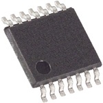
| 描述 | IC OPAMP GP 15MHZ RRO 14TSSOP |
| 产品分类 | Linear - Amplifiers - Instrumentation, OP Amps, Buffer Amps |
| 品牌 | Analog Devices Inc |
| 数据手册 | |
| 产品图片 |
|
| 产品型号 | OP462HRUZ-REEL |
| rohs | 无铅 / 符合限制有害物质指令(RoHS)规范要求 |
| 产品系列 | - |
| 产品培训模块 | http://www.digikey.cn/PTM/IndividualPTM.page?site=cn&lang=zhs&ptm=30008http://www.digikey.cn/PTM/IndividualPTM.page?site=cn&lang=zhs&ptm=26202 |
| 产品目录页面 | |
| 供应商器件封装 | 14-TSSOP |
| 其它名称 | OP462HRUZ-REEL-ND |
| 包装 | 带卷 (TR) |
| 压摆率 | 13 V/µs |
| 增益带宽积 | 15MHz |
| 安装类型 | 表面贴装 |
| 封装/外壳 | 14-TSSOP(0.173",4.40mm 宽) |
| 工作温度 | -40°C ~ 125°C |
| 放大器类型 | 通用 |
| 标准包装 | 2,500 |
| 电压-电源,单/双 (±) | 2.7 V ~ 12 V, ±1.35 V ~ 6 V |
| 电压-输入失调 | 25µV |
| 电流-电源 | 550µA |
| 电流-输入偏置 | 260nA |
| 电流-输出/通道 | 30mA |
| 电路数 | 4 |
| 视频文件 | http://www.digikey.cn/classic/video.aspx?PlayerID=1364138032001&width=640&height=505&videoID=2245193153001http://www.digikey.cn/classic/video.aspx?PlayerID=1364138032001&width=640&height=505&videoID=2245193159001 |
| 输出类型 | 满摆幅 |


- 商务部:美国ITC正式对集成电路等产品启动337调查
- 曝三星4nm工艺存在良率问题 高通将骁龙8 Gen1或转产台积电
- 太阳诱电将投资9.5亿元在常州建新厂生产MLCC 预计2023年完工
- 英特尔发布欧洲新工厂建设计划 深化IDM 2.0 战略
- 台积电先进制程称霸业界 有大客户加持明年业绩稳了
- 达到5530亿美元!SIA预计今年全球半导体销售额将创下新高
- 英特尔拟将自动驾驶子公司Mobileye上市 估值或超500亿美元
- 三星加码芯片和SET,合并消费电子和移动部门,撤换高东真等 CEO
- 三星电子宣布重大人事变动 还合并消费电子和移动部门
- 海关总署:前11个月进口集成电路产品价值2.52万亿元 增长14.8%


PDF Datasheet 数据手册内容提取
15 MHz Rail-to-Rail Operational Amplifiers Data Sheet OP162/OP262/OP462 FEATURES PIN CONFIGURATIONS Wide bandwidth: 15 MHz NULL 1 8 NULL Low offset voltage: 325 µV max –IN A 2 OP162 7 V+ Low noise: 9.5 nV/√Hz @ 1 kHz +IN A 3 TOP VIEW 6 OUT A SRLoianwigl- TlteoC--sVruapil: p o1lu yµt Vopp/u°etC rs atwytipion ng: 2.7 V to 12 V V– N4C( =N oNtO to C SOcNaNleE)CT5 NC 00288-001 OS High slew rate: 13 V/µs Figure 1. 8-Lead Narrow-Body SOIC (S Suffix) No phase inversion Unity-gain stable OUT A 1 8 V+ –IN A 2 OP262 7 OUT B APPLICATIONS TOP VIEW PSoamrtapblilneg i nAsDtrCu ammepnltiafiteior n +INV A– 34 (Not to Scale) 65 –+IINN BB 00288-004 Wireless LANs Figure 2. 8-Lead TSSOP (RU Suffix) and 8-Lead Narrow-Body SOIC (S Suffix) Direct access arrangement Office automation OUT A 1 14 OUT D –IN A 2 13 –IN D +IN A 3 OP462 12 +IN D GENERAL DESCRIPTION TOP VIEW V+ 4 (Not to Scale) 11 V– The OP162 (single), OP262 (dual), and OP462 (quad) rail-to- +IN B 5 10 +IN C rail 15 MHz amplifiers feature the extra speed new designs –IN B 6 9 –IN C require, with the benefits of precision and low power operation. OUT B 7 8 OUT C 00288-006 With their incredibly low offset voltage of 45 µV (typical) and Figure 3. 14-Lead Narrow-Body SOIC (S Suffix) and low noise, they are perfectly suited for precision filter applica- 14-Lead TSSOP (RU Suffix) tions and instrumentation. The low supply current of 500 µA (typical) is critical for portable or densely packed designs. In addition, the rail-to-rail output swing provides greater dynamic range and control than standard video amplifiers. These products operate from single supplies as low as 2.7 V to dual supplies of ±6 V. The fast settling times and wide output swings recommend them for buffers to sampling A/D converters. The output drive of 30 mA (sink and source) is needed for many audio and display applications; more output current can be supplied for limited durations. The OPx62 family is specified over the extended industrial temperature range (–40°C to +125°C). The single OP162 amplifiers are available in 8-lead SOIC package. The dual OP262 amplifiers are available in 8-lead SOIC and TSSOP packages. The quad OP462 amplifiers are available in 14-lead, narrow-body SOIC and TSSOP packages. Rev. H Document Feedback Information furnished by Analog Devices is believed to be accurate and reliable. However, no responsibility is assumed by Analog Devices for its use, nor for any infringements of patents or other One Technology Way, P.O. Box 9106, Norwood, MA 02062-9106, U.S.A. rights of third parties that may result from its use. Specifications subject to change without notice. No license is granted by implication or otherwise under any patent or patent rights of Analog Devices. Tel: 781.329.4700 ©2013 Analog Devices, Inc. All rights reserved. Trademarks and registered trademarks are the property of their respective owners. Technical Support www.analog.com
OP162/OP262/OP462 Data Sheet TABLE OF CONTENTS Features .............................................................................................. 1 Input Overvoltage Protection ................................................... 13 Applications ....................................................................................... 1 Output Phase Reversal ............................................................... 13 General Description ......................................................................... 1 Power Dissipation....................................................................... 13 Pin Configurations ........................................................................... 1 Unused Amplifiers ..................................................................... 14 Revision History ............................................................................... 2 Power-On Settling Time ............................................................ 14 Specifications ..................................................................................... 3 Capacitive Load Drive ............................................................... 14 Absolute Maximum Ratings ............................................................ 6 Total Harmonic Distortion and Crosstalk .............................. 15 ESD Caution .................................................................................. 6 PCB Layout Considerations ...................................................... 15 Typical Performance Characteristics ............................................. 7 Applications Circuits ...................................................................... 16 Applications ..................................................................................... 12 Single-Supply Stereo Headphone Driver................................. 16 Functional Description .............................................................. 12 Instrumentation Amplifier........................................................ 16 Offset Adjustment ...................................................................... 12 Direct Access Arrangement ...................................................... 17 Rail-to-Rail Output .................................................................... 12 Outline Dimensions ....................................................................... 18 Output Short-Circuit Protection .............................................. 12 Ordering Guide .......................................................................... 20 REVISION HISTORY 4/13—Rev. G to Rev. H 12/04—Rev. D to Rev. E Combined Figure 2 and Figure 3; Combined Figure 4 and Updated Format .................................................................. Universal Figure 5 .............................................................................................. 1 Changes to General Description ..................................................... 1 Changes to Figure 12 ........................................................................ 9 Changes to Specifications ................................................................. 3 Changes to Package Type ................................................................. 6 5/12—Rev. F to Rev. G Change to Figure 16 .......................................................................... 8 Deleted MSOP Throughout ............................................................ 1 Change to Figure 22 .......................................................................... 9 Deleted Figure 2; Renumbered Sequentially................................. 1 Change to Figure 36 ....................................................................... 13 Deleted Spice-Macro Model Section ............................................ 18 Change to Figure 37 ....................................................................... 14 Updated Outline Dimensions ....................................................... 18 Changes to Ordering Guide .......................................................... 20 Changes to Ordering Guide .......................................................... 20 10/02—Rev. C to Rev. D 1/05—Rev. E to Rev. F Deleted 8-Lead Plastic DIP (N-8) .................................... Universal Changes to Absolute Maximum Ratings Table 4 and Table 5 .... 6 Deleted 14-Lead Plastic DIP (N-14) ................................ Universal Change to Figure 36 ....................................................................... 13 Edits to ORDERING GUIDE ....................................................... 19 Changes to Ordering Guide .......................................................... 20 Edits to Figure 30 ............................................................................ 19 Edits to Figure 31 ............................................................................ 19 Updated Outline Dimensions ....................................................... 19 Rev. H | Page 2 of 20
Data Sheet OP162/OP262/OP462 SPECIFICATIONS @ V = 5.0 V, V = 0 V, T = 25°C, unless otherwise noted. S CM A Table 1. Electrical Characteristics Parameter Symbol Conditions Min Typ Max Unit INPUT CHARACTERISTICS Offset Voltage V OP162G, OP262G, OP462G 45 325 µV OS –40°C ≤ T ≤ +125°C 800 µV A H grade, –40°C ≤ T ≤ +125°C 1 mV A D grade 0.8 3 mV –40°C ≤ T ≤ +125°C 5 mV A Input Bias Current I 360 600 nA B –40°C ≤ T ≤ +125°C 650 nA A Input Offset Current I ±2.5 ±25 nA OS –40°C ≤ T ≤ +125°C ±40 nA A Input Voltage Range V 0 4 V CM Common-Mode Rejection CMRR 0 V ≤ V ≤ 4.0 V, –40°C ≤ T ≤ +125°C 70 110 dB CM A Large Signal Voltage Gain A R = 2 kΩ, 0.5 ≤ V ≤ 4.5 V 30 V/mV VO L OUT R = 10 kΩ, 0.5 ≤ V ≤ 4.5 V 65 88 V/mV L OUT R = 10 kΩ, –40°C ≤ T ≤ +125°C 40 V/mV L A Long-Term Offset Voltage1 V G grade 600 µV OS Offset Voltage Drift2 ∆VOS/∆T 1 µV/°C Bias Current Drift ∆IB/∆T 250 pA/°C OUTPUT CHARACTERISTICS Output Voltage Swing High V I = 250 µA, –40°C ≤ T ≤ +125°C 4.95 4.99 V OH L A I = 5 mA 4.85 4.94 V L Output Voltage Swing Low V I = 250 µA, –40°C ≤T ≤ +125°C 14 50 mV OL L A I = 5 mA 65 150 mV L Short-Circuit Current I Short to ground ±80 mA SC Maximum Output Current IOUT ±30 mA POWER SUPPLY Power Supply Rejection Ratio PSRR V = 2.7 V to 7 V 120 dB S –40°C ≤ T ≤ +125°C 90 dB A Supply Current/Amplifier I OP162, V = 2.5 V 600 750 µA SY OUT –40°C ≤ T ≤ +125°C 1 mA A OP262, OP462, V = 2.5 V 500 700 µA OUT –40°C ≤ T ≤ +125°C 850 µA A DYNAMIC PERFORMANCE Slew Rate SR 1 V < V < 4 V, R = 10 kΩ 10 V/µs OUT L Settling Time t To 0.1%, A = –1, V = 2 V step 540 ns S V O Gain Bandwidth Product GBP 15 MHz Phase Margin φ 61 Degrees m NOISE PERFORMANCE Voltage Noise e p-p 0.1 Hz to 10 Hz 0.5 µV p-p n Voltage Noise Density en f = 1 kHz 9.5 nV/√Hz Current Noise Density in f = 1 kHz 0.4 pA/√Hz 1 Long-term offset voltage is guaranteed by a 1000 hour life test performed on three independent lots at 125°C, with an LTPD of 1.3. 2 Offset voltage drift is the average of the −40°C to +25°C delta and the +25°C to +125°C delta. Rev. H | Page 3 of 20
OP162/OP262/OP462 Data Sheet @ V = 3.0 V, V = 0 V, T = 25°C, unless otherwise noted. S CM A Table 2. Electrical Characteristics Parameter Symbol Conditions Min Typ Max Unit INPUT CHARACTERISTICS Offset Voltage V OP162G, OP262G, OP462G 50 325 µV OS G, H grades, –40°C ≤ T ≤ +125°C 1 mV A D grade 0.8 3 mV –40°C ≤ T ≤ +125°C 5 mV A Input Bias Current I 360 600 nA B Input Offset Current I ±2.5 ±25 nA OS Input Voltage Range V 0 2 V CM Common-Mode Rejection CMRR 0 V ≤ V ≤ 2.0 V, –40°C ≤ T ≤ +125°C 70 110 dB CM A Large Signal Voltage Gain A R = 2 kΩ, 0.5 V ≤ V ≤ 2.5 V 20 V/mV VO L OUT R = 10 kΩ, 0.5 V ≤ V ≤ 2.5 V 20 30 V/mV L OUT Long-Term Offset Voltage1 V G grade 600 µV OS OUTPUT CHARACTERISTICS Output Voltage Swing High V I = 250 µA 2.95 2.99 V OH L I= 5 mA 2.85 2.93 V L Output Voltage Swing Low V I = 250 µA 14 50 mV OL L I= 5 mA 66 150 mV L POWER SUPPLY Power Supply Rejection Ratio PSRR V = 2.7 V to 7 V, S –40°C ≤ T ≤ +125°C 60 110 dB A Supply Current/Amplifier I OP162, V = 1.5 V 600 700 µA SY OUT –40°C ≤ T ≤ +125°C 1 mA A OP262, OP462, V = 1.5 V 500 650 µA OUT –40°C ≤ T ≤ +125°C 850 µA A DYNAMIC PERFORMANCE Slew Rate SR R = 10 kΩ 10 V/µs L Settling Time t To 0.1%, A = –1, V = 2 V step 575 ns S V O Gain Bandwidth Product GBP 15 MHz Phase Margin φ 59 Degrees m NOISE PERFORMANCE Voltage Noise e p-p 0.1 Hz to 10 Hz 0.5 µV p-p n Voltage Noise Density en f = 1 kHz 9.5 nV/√Hz Current Noise Density in f = 1 kHz 0.4 pA/√Hz 1 Long-term offset voltage is guaranteed by a 1000 hour life test performed on three independent lots at 125°C, with an LTPD of 1.3. Rev. H | Page 4 of 20
Data Sheet OP162/OP262/OP462 @ V = ±5.0 V, V = 0 V, T = 25°C, unless otherwise noted. S CM A Table 3. Electrical Characteristics Parameter Symbol Conditions Min Typ Max Unit INPUT CHARACTERISTICS Offset Voltage VOS OP162G, OP262G, OP462G 25 325 µV −40°C ≤ TA ≤ +125°C 800 µV H grade, –40°C ≤ T ≤ +125°C 1 mV A D grade 0.8 3 mV −40°C ≤ TA ≤ +125°C 5 mV Input Bias Current IB 260 500 nA −40°C ≤ TA ≤ +125°C 650 nA Input Offset Current IOS ±2.5 ±25 nA −40°C ≤ TA ≤ +125°C ±40 nA Input Voltage Range VCM –5 +4 V Common-Mode Rejection CMRR −4.9 V ≤ VCM ≤ +4.0 V, –40°C ≤ TA ≤ +125°C 70 110 dB Large Signal Voltage Gain AVO RL = 2 kΩ, –4.5 V ≤ VOUT ≤ +4.5 V 35 V/mV R = 10 kΩ, –4.5 V ≤ V ≤ +4.5 V 75 120 V/mV L OUT −40°C ≤ TA ≤ +125°C 25 V/mV Long-Term Offset Voltage1 VOS G grade 600 µV Offset Voltage Drift2 ∆VOS/∆T 1 µV/°C Bias Current Drift ∆IB/∆T 250 pA/°C OUTPUT CHARACTERISTICS Output Voltage Swing High VOH IL = 250 µA, –40°C ≤ TA ≤ +125°C 4.95 4.99 V I= 5 mA 4.85 4.94 V L Output Voltage Swing Low VOL IL = 250 µA, –40°C ≤ TA ≤ +125°C –4.99 –4.95 V I= 5 mA –4.94 –4.85 V L Short-Circuit Current ISC Short to ground ±80 mA Maximum Output Current IOUT ±30 mA POWER SUPPLY Power Supply Rejection Ratio PSRR V = ±1.35 V to ±6 V, S −40°C ≤ TA ≤ +125°C 60 110 dB Supply Current/Amplifier ISY OP162, VOUT = 0 V 650 800 µA −40°C ≤ TA ≤ +125°C 1.15 mA OP262, OP462, V = 0 V 550 775 µA OUT −40°C ≤ TA ≤ +125°C 1 mA Supply Voltage Range VS 3.0 (±1.5) 12 (±6) V DYNAMIC PERFORMANCE Slew Rate SR −4 V < VOUT < 4 V, RL = 10 kΩ 13 V/µs Settling Time tS To 0.1%, AV = –1, VO = 2 V step 475 ns Gain Bandwidth Product GBP 15 MHz Phase Margin φm 64 Degrees NOISE PERFORMANCE Voltage Noise e p-p 0.1 Hz to 10 Hz 0.5 µV p-p n Voltage Noise Density en f = 1 kHz 9.5 nV/√Hz Current Noise Density in f = 1 kHz 0.4 pA/√Hz 1 Long-term offset voltage is guaranteed by a 1000 hour life test performed on three independent lots at +125°C, with an LTPD of 1.3. 2 Offset voltage drift is the average of the −40°C to +25°C delta and the +25°C to +125°C delta. Rev. H | Page 5 of 20
OP162/OP262/OP462 Data Sheet ABSOLUTE MAXIMUM RATINGS Stresses above those listed under Absolute Maximum Ratings Table 4. may cause permanent damage to the device. This is a stress Parameter Min rating only; functional operation of the device at these or any Supply Voltage ±6 V other conditions above those indicated in the operational Input Voltage1 ±6 V section of this specification is not implied. Exposure to absolute Differential Input Voltage2 ±0.6 V maximum rating conditions for extended periods may affect Internal Power Dissipation device reliability. SOIC (S) Observe Derating Curves TSSOP (RU) Observe Derating Curves Table 5. Output Short-Circuit Duration Observe Derating Curves Package Type θJA1 θJC Unit Storage Temperature Range –65°C to +150°C 8-Lead SOIC (S) 157 56 °C/W Operating Temperature Range –40°C to +125°C 8-Lead TSSOP (RU) 208 °C/W Junction Temperature Range –65°C to +150°C 14-Lead SOIC (S) 105 °C/W Lead Temperature Range 14-Lead TSSOP (RU) 148 °C/W (Soldering, 10 sec) 300°C 1 θJA is specified for the worst-case conditions, that is, θJA is specified for a 1 For supply voltages greater than 6 V, the input voltage is limited to less than device soldered in circuit board for SOIC, and TSSOP packages. or equal to the supply voltage. 2 For differential input voltages greater than 0.6 V, the input current should be ESD CAUTION limited to less than 5 mA to prevent degradation or destruction of the input devices. Rev. H | Page 6 of 20
Data Sheet OP162/OP262/OP462 TYPICAL PERFORMANCE CHARACTERISTICS 250 125 VS = 5V VS = 5V 200 TCAO =U N25T° =C V) 100 ers) 720 OP AMPS µGE ( mplifi 150 OLTA 75 A V NTITY ( 100 FFSET 50 A O QU UT P N 50 I 25 0 00288-007 0 00288-010 –200 –140 –80 –20 40 100 160 –75 –50 –25 0 25 50 75 100 125 150 INPUT OFFSET VOLTAGE (µV) TEMPERATURE (°C) Figure 4. OP462 Input Offset Voltage Distribution Figure 7. OP462 Input Offset Voltage vs. Temperature 100 0 VS = 5V VS = 5V 80 TA = 25°C COUNT = –100 mplifiers) 60 360 OP AMPS RENT (nA) –200 A R Y ( CU ANTIT 40 BIAS –300 U T Q U P N 20 I –400 00.2 0.3 0.5 0.7 0.9 1.1 1.3 1.5 00288-008 –500 00288−011 –50 –25 0 25 50 75 100 125 150 INPUT OFFSET DRIFT, TCVOS (µV,°C) TEMPERATURE (°C) Figure 5. OP462 Input Offset Voltage Drift (TCVOS) Figure 8. OP462 Input Bias Current vs. Temperature 420 15 VS = 5V VS = 5V 340 A) T (nA) ENT (n 10 N R E R R U R 260 C T CU SET U F INP T OF 5 180 U P N I 1000 0.5 1.0 1.5 2.0 2.5 3.0 3.5 4.000288-009 0 00288−012 –75 –50 –25 0 25 50 75 100 125 150 COMMON-MODE VOLTAGE (V) TEMPERATURE (°C) Figure 6. OP462 Input Bias Current vs. Common-Mode Voltage Figure 9. OP462 Input Offset Current vs. Temperature Rev. H | Page 7 of 20
OP162/OP262/OP462 Data Sheet 5.12 100 VS = 5V GH VOLTAGE (V) 55..0060 IOUT = 250µA W VOLTAGE (mV) 8600 VS = 10V OUTPUT HI 4.94 IOUT = 5mA OUTPUT LO 40 VS = 3V 4.88 20 4.82 00288-013 0 00288-016 –75 –50 –25 0 25 50 75 100 125 150 0 1 2 3 4 5 6 7 TEMPERATURE (°C) LOAD CURRENT (mA) Figure 10. OP462 Output High Voltage vs. Temperature Figure 13. Output Low Voltage to Supply Rail vs. Load Current 0.100 1.0 VS = 5V 0.9 AGE (mV)0.080 IOUT = 5mA NT (mA) 000...876 VS = 5V VS = 10V VOLT0.060 URRE 0.5 VS = 3V W C TPUT LO0.040 SUPPLY 00..43 U O0.020 0.2 0.000–75 –50 –25 0 25 IOU5T0 = 2507µ5A 100 125 15000288-014 0.10–75 –50 –25 0 25 75 100 125 15000288-017 TEMPERATURE (°C) TEMPERATURE (°C) Figure 11. OP462 Output Low Voltage vs. Temperature Figure 14. Supply Current/Amplifier vs. Temperature 100 0.7 RL = 10kΩ TA = 25°C 80 GAIN (V/mV) 60 VS = 5V URRENT (mA) 0.6 P C O Y LO 40 PL 0.5 PEN- RL = 2kΩ SUP O 20 0 RL = 600Ω 00288-015 0.40 2 4 6 8 10 1200288-018 –75 –50 –25 0 25 50 75 100 125 150 SUPPLY VOLTAGE (V) TEMPERATURE (°C) Figure 12. OP462 Open-Loop Gain vs. Temperature Figure 15. OP462 Supply Current/Amplifier vs. Supply Voltage Rev. H | Page 8 of 20
Data Sheet OP162/OP262/OP462 50 4 VS = 5V 40 GAIN TA = 25°C 3 0.1% 0.01% 30 45 2 VTAS == 255V°C B) N (dB) 2100 PHASE 91035 SHIFT (d SIZE (V) 10 AI E P G S E 0 180 HA ST –1 P –10 225 –2 0.1% 0.01% ––2300 270 00288-019 ––34 00288-022 100k 1M 10M 100M 0 200 400 600 800 1000 FREQUENCY (Hz) SETTLING TIME (nS) Figure 16. Open-Loop Gain and Phase vs. Frequency (No Load) Figure 19. Step Size vs. Settling Time 60 60 B) 40 VTRCASLL ==== 25855V3p°0FCΩ 50 VTTRAASL ==== ±25155V00°kCmΩV d N ( %) 40 GAI 20 T ( ED-LOOP 0 VERSHOO 30 +OS –OS OS O 20 L C –20 10 –30 00288-020 0 00288-023 10k 100k 1M 10M 100M 10 100 1000 FREQUENCY (Hz) CAPACITANCE (pF) Figure 17. Closed-Loop Gain vs. Frequency Figure 20. Small-Signal Overshoot vs. Capacitance 5 70 VS = 5V p-p) 4 60 TA = 25°C MAXIMUM OUTPUT SWING (V 321 VARCSVLL C===L 511 =V05 kp1ΩF √NOISE DENSITY (nV/Hz) 54320000 0 TDAIS =T O25R°TCION<1% 00288-021 100 00288-024 10k 100k 1M 10M 1 10 100 1k FREQUENCY (Hz) FREQUENCY (Hz) Figure 18. Maximum Output Swing vs. Frequency Figure 21. Voltage Noise Density vs. Frequency Rev. H | Page 9 of 20
OP162/OP262/OP462 Data Sheet 7 90 VS = 5V VS = 5V 6 TA = 25°C 80 TA = 25°C Hz) 5 70 √ A/ SITY (p 4 R (dB) 60 +PSRR –PSRR N R DE 3 PS 50 E S NOI 2 40 10 00288-025 3200 00288-028 1 10 100 1k 1k 10k 100k 1M 10M FREQUENCY (Hz) FREQUENCY (Hz) Figure 22. Current Noise Density vs. Frequency Figure 25. PSRR vs. Frequency 300 VS = 5V 20mV 2s TA = 25°C 250 100 Ω) 90 E ( 200 C N A D E P 150 T IM AVCL = 10 U TP 100 OU 10 AVCL = 1 0% VS = 5V 500 00288-026 AenV == 01.050µkVΩ p-p 00288-029 100k 1M 10M FREQUENCY (Hz) Figure 23. Output Impedance vs. Frequency Figure 26. 0.1 Hz to 10 Hz Noise 90 80 VTAS == 255V°C 2V VVISN == ±152VV p-p 100 AV = 1 90 70 dB) 60 R ( R M C 50 40 10 0% 3200 00288-027 2V 20µs 00288-030 1k 10k 100k 1M 10M FREQUENCY (Hz) Figure 24. CMRR vs. Frequency Figure 27. No Phase Reversal (VIN = 12 V p-p, VS = ±5 V, AV = 1) Rev. H | Page 10 of 20
Data Sheet OP162/OP262/OP462 VS = 5V 19000 VATASV === 2515V°C 19000 ATCAVL === 21150°0CpF CL = 100pF 10 10 0% 0% 20mV 200ns 00288-031 500mV 100µs 00288-032 Figure 28. Small Signal Transient Response Figure 29. Large Signal Transient Response Rev. H | Page 11 of 20
OP162/OP262/OP462 Data Sheet APPLICATIONS FUNCTIONAL DESCRIPTION OFFSET ADJUSTMENT The OPx62 family is fabricated using Analog Devices’ high Because the OP162/OP262/OP462 have an exceptionally low speed complementary bipolar process, also called XFCB. This typical offset voltage, adjustment to correct offset voltage may process trench isolates each transistor to lower parasitic capaci- not be needed. However, the OP162 has pinouts to attach a tances for high speed performance. This high speed process has nulling resistor. Figure 31 shows how the OP162 offset voltage been implemented without sacrificing the excellent transistor can be adjusted by connecting a potentiometer between Pin 1 matching and overall dc performance characteristic of Analog and Pin 8, and connecting the wiper to V . It is important to CC Devices’ complementary bipolar process. This makes the OPx62 avoid accidentally connecting the wiper to V , as this can damage EE family an excellent choice as an extremely fast and accurate low the device. The recommended value for the potentiometer is voltage op amp. 20 kΩ. Figure 30 shows a simplified equivalent schematic for the OP162. +5V A PNP differential pair is used at the input of the device. The cross connecting of the emitters lowers the transconductance of 1 20kΩ 8 the input stage improving the slew rate of the device. Lowering 3 7 the transconductance through cross connecting the emitters has OP162 6 VOS another advantage in that it provides a lower noise factor than if 4 emitter degeneration resistors were used. The input stage can 2 function with the base voltages taken all the way to the negative –5V 00288-034 power supply, or up to within 1 V of the positive power supply. Figure 31. Offset Adjustment Schematic VCC RAIL-TO-RAIL OUTPUT The OP162/OP262/OP462 have a wide output voltage range that extends to within 60 mV of each supply rail with a load current of 5 mA. Decreasing the load current extends the output voltage range even closer to the supply rails. The common-mode input range extends from ground to within 1 V of the positive +IN supply. It is recommended that there be some minimal amount –IN VOUT of gain when a rail-to-rail output swing is desired. The minimum gain required is based on the supply voltage and can be found as V A = S V,min V −1 S VEE 00288-033 vwohlteargee V oSf i 5s tVh,e t hpeo smitiinveim suupmp lgya vino lttoag aec.h Wieivteh raa isli-ntogl-er-asiul opupltyp ut Figure 30. Simplified Schematic should be 1.25. Two complementary transistors in a common-emitter OUTPUT SHORT-CIRCUIT PROTECTION configuration are used for the output stage. This allows the To achieve a wide bandwidth and high slew rate, the output of output of the device to swing to within 50 mV of either supply the OP162/OP262/OP462 are not short-circuit protected. Shorting rail at load currents less than 1 mA. As load current increases, the output directly to ground or to a supply rail may destroy the the maximum voltage swing of the output decreases. This is due device. The typical maximum safe output current is ±30 mA. to the collector-to-emitter saturation voltages of the output Steps should be taken to ensure the output of the device will not transistors increasing. The gain of the output stage, and conse- be forced to source or sink more than 30 mA. quently the open-loop gain of the amplifier, is dependent on the In applications where some output current protection is needed, load resistance connected at the output. Because the dominant pole but not at the expense of reduced output voltage headroom, a frequency is inversely proportional to the open-loop gain, the low value resistor in series with the output can be used. This is unity-gain bandwidth of the device is not affected by the load shown in Figure 32. The resistor is connected within the feed- resistance. This is typically the case in rail-to-rail output back loop of the amplifier so that if V is shorted to ground devices. OUT Rev. H | Page 12 of 20
Data Sheet OP162/OP262/OP462 and V swings up to 5 V, the output current will not exceed To calculate the internal junction temperature of the OPx62, use IN 30 mA. For single 5 V supply applications, resistors less than the formula 169 Ω are not recommended. T = P × θ + T J DISS JA A 5V where: T is the OPx62 junction temperature. J VIN 169Ω PDISS is the OPx62 power dissipation. OPx62 VOUT θJA is the OPx62 package thermal resistance, junction-to- ambient temperature. 00288-035 TTAh eis p tohwe earm dbiisesnipt atteemd pbeyr tahtuer dee ovfi cthe ec acnir cbuei tc.a lculated as Figure 32. Output Short-Circuit Protection P = I × (V – V ) INPUT OVERVOLTAGE PROTECTION DISS LOAD S OUT where: The input voltage should be limited to ±6 V, or damage to the I is the OPx62 output load current. device can occur. Electrostatic protection diodes placed in the LOAD V is the OPx62 supply voltage. input stage of the device help protect the amplifier from static S V is the OPx62 output voltage. discharge. Diodes are connected between each input as well as OUT from each input to both supply pins as shown in the simplified Figure 33 and Figure 34 provide a convenient way to determine equivalent circuit in Figure 30. If an input voltage exceeds either if the device is being overheated. The maximum safe power supply voltage by more than 0.6 V, or if the differential input dissipation can be found graphically, based on the package type voltage is greater than 0.6 V, these diodes energize causing and the ambient temperature around the package. By using the overvoltage damage. previous equation, it is a simple matter to see if PDISS exceeds the device’s power derating curve. To ensure proper operation, it is The input current should be limited to less than 5 mA to important to observe the recommended derating curves shown prevent degradation or destruction of the device by placing an in Figure 33 and Figure 34. external resistor in series with the input at risk of being overdriven. The size of the resistor can be calculated by dividing the maxi- 0.9 mum input voltage by 5 mA. For example, if the differential s) 0.8 input voltage could reach 5 V, the external resistor should be att W 5 V/5 mA = 1 kΩ. In practice, this resistor should be placed in ON ( 0.7 8-LEAD SOIC series with both inputs to balance any offset voltages created by ATI 0.6 P the input bias current. SSI 0.5 OUTPUT PHASE REVERSAL R DI 8-LEAD MSOP E 0.4 OW 8-LEAD TSSOP The OP162/OP262/OP462 are immune to phase reversal as P 0.3 M long as the input voltage is limited to ±6 V. Figure 27 shows the U M 0.2 output of a device with the input voltage driven beyond the AXI spuhpapsely, lvaorgltea gceusr.r Aenltths oduugeh t oth ien pduetv iocvee’sr ovuotltpaugte d cooeusl dn oret scuhlat,n ge M 0.10 00288-036 20 40 60 80 100 120 damaging the device. In applications where the possibility of an AMBIENT TEMPERATURE (°C) input voltage exceeding the supply voltage exists, overvoltage Figure 33. Maximum Power Dissipation vs. Temperature for 8-Lead Package Types protection should be used, as described in the previous section. POWER DISSIPATION The maximum power that can be safely dissipated by the OP162/OP262/OP462 is limited by the associated rise in junction temperature. The maximum safe junction temperature is 150°C; device performance suffers when this limit is exceeded. If this maximum is only momentarily exceeded, proper circuit operation will be restored as soon as the die temperature is reduced. Leaving the device in an “overheated” condition for an extended period can result in permanent damage to the device. Rev. H | Page 13 of 20
OP162/OP262/OP462 Data Sheet 1.2 1 Watts) 11..01 0S QTOUA +R5EV N ( 14-LEAD SOIC O 0.9 ATI 0.8 OP462 VOUT SSIP 0.7 10KΩ OWER DI 00..56 14-LEAD TSSOP 00288-039 M P 0.4 Figure 36. Test Circuit for Power-On Settling Time MU 0.3 CAPACITIVE LOAD DRIVE AXI 0.2 M 0.10 00288-037 Tdehvei cOePs 1th6a2t/ OtoPle2r6a2te/ OsoPm46e2 c aarpea chiitgivhe s lpoeaeddin, egx attr etmheeilry o auctcpuurtast.e A s 20 45 70 95 120 AMBIENT TEMPERATURE (°C) load capacitance increases, unity-gain bandwidth of an OPx62 Figure 34. Maximum Power Dissipation vs. Temperature for device decreases. This also causes an increase in overshoot and 14-Lead Package Types settling time for the output. Figure 38 shows an example of this UNUSED AMPLIFIERS with the device configured for unity gain and driving a 10 kΩ resistor and 300 pF capacitor placed in parallel. It is recommended that any unused amplifiers in a dual or a By connecting a series R-C network, commonly called a quad package be configured as a unity-gain follower with a “snubber” network, from the output of the device to ground, 1 kΩ feedback resistor connected from the inverting input to this ringing can be eliminated and overshoot can be the output, and the noninverting input tied to the ground plane. significantly reduced. Figure 37 shows how to set up the POWER-ON SETTLING TIME snubber network, and Figure 39 shows the improvement in The time it takes for the output of an op amp to settle after a output response with the network added. supply voltage is delivered can be an important consideration in 5V some power-up-sensitive applications. An example of this would be in an A/D converter where the time until valid data can be produced after power-up is important. OPx62 VOUT The OPx62 family has a rapid settling time after power-up. VIN RX CL Fsuigpuprlye 3v5o lstahgoew osf t VheS =O P+456 V2. oTuhtep utet sste ctitrlicnugit t iinm Fesig fuorre a 3 s6i nwgales- CX 00288-040 used to find the power-on settling times for the device. Figure 37. Snubber Network Compensation for Capacitive Loads 2V 500ns VASV == 51V 100 CL = 300pF 100 90 RL = 10kΩ 90 VS = 5V AV = 1 10 RL = 10kΩ 10 0% 0% 50mV 00288-038 50mV 1µs 00288-041 Figure 35. Oscilloscope Photo of VS and VOUT Figure 38. A Photo of a Ringing Square Wave Rev. H | Page 14 of 20
Data Sheet OP162/OP262/OP462 Figure 42 shows the worst case crosstalk between two amplifiers VS = 5V in the OP462. A 1 V rms signal is applied to one amplifier while AV = 1 100 CL = 300pF measuring the output of an adjacent amplifier. Both amplifiers 90 RL = 10kΩ are configured for unity gain and supplied with ±2.5 V. WITH SNUBBER: RX = 140Ω 0.010 CX = 10nF VS =±2.5V AV = 1 VIN = 1.0V rms RL = 10kΩ BANDWIDTH: 10 <10Hz TO 22kHz 0% %) N ( 50mV 1µs 00288-042 THD+0.001 Figure 39. A Photo of a Nice Square Wave at the Output The network operates in parallel with the load capacitor, C , L avnaldu epsr oovf itdhees nceotmwpoerkn sraetsiiosnto fro arn tdh ec aapdadceidto pr haarsee e lmagp. iTrihcael alyc tual 0.0001 00288-044 20 100 1k 10k 20k determined to minimize overshoot and maximize unity-gain FREQUENCY (Hz) bandwidth. Table 6 shows a few sample snubber networks for Figure 41. THD + N vs. Frequency large load capacitors. –40 Table 6. Snubber Networks for Large Capacitive Loads –50 AVIVN == 11.0V rms C<L 3OA0D0 pF 1R4X 0 Ω 1C0X nF –60 RV SL == ±1 (200.kd5Ω�BVV) –70 500 pF 100 Ω 10 nF V) –80 1 nF 80 Ω 10 nF dB K ( –90 10 nF 10 Ω 47 nF L A XT –100 Higher load capacitance will reduce the unity-gain bandwidth –110 of the device. Figure 40 shows unity-gain bandwidth vs. capacitive load. The snubber network does not provide any –120 ionvcerresahsoeo itn, absa snhdowwidnt bhe, tbwuet eint sFuibgsutraen 3ti8a lalyn dre Fdiugcuerse r3in9.g ing and ––114300 00288-045 20 100 1k 10k 20k 10 FREQUENCY (Hz) Figure 42. Crosstalk vs. Frequency 9 PCB LAYOUT CONSIDERATIONS 8 Hz) 7 Because the OP162/OP262/OP462 can provide gains at high H (M 6 frequency, careful attention to board layout and component T selection is recommended. As with any high speed application, D 5 WI a good ground plane is essential to achieve the optimum D N 4 A performance. This can significantly reduce the undesirable B 3 effects of ground loops and I × R losses by providing a low 2 impedance reference point. Best results are obtained with a 10 00288-043 mplaunlteil. ayer board design with one layer assigned to ground 10pF 100pF 1nF 10nF CLOAD Use chip capacitors for supply bypassing, with one end of the Figure 40. Unity-Gain Bandwidth vs. CLOAD capacitor connected to the ground plane and the other end connected within 1/8 inch of each power pin. An additional TOTAL HARMONIC DISTORTION AND CROSSTALK large tantalum electrolytic capacitor (4.7 µF to 10 µF) should be The OPx62 device family offers low total harmonic distortion connected in parallel. This capacitor provides current for fast, making it an excellent choice for audio applications. Figure 41 large-signal changes at the device’s output; therefore, it does not shows a graph of THD plus noise figures at 0.001% for the need to be placed as close to the supply pins. OP462. Rev. H | Page 15 of 20
OP162/OP262/OP462 Data Sheet APPLICATIONS CIRCUITS SINGLE-SUPPLY STEREO HEADPHONE DRIVER INSTRUMENTATION AMPLIFIER Figure 43 shows a stereo headphone output amplifier that can Because of their high speed, low offset voltages, and low noise operate from a single 5 V supply. The reference voltage is characteristics, the OP162/OP262/OP462 can be used in a wide derived by dividing the supply voltage down with two 100 kΩ variety of high speed applications, including precision instru- resistors. A 10 µF capacitor prevents power supply noise from mentation amplifiers. Figure 44 shows an example of such an contaminating the audio signal and establishes an ac ground for application. the volume control potentiometers. –VIN The audio signal is ac-coupled to each noninverting input OP462-A 2kΩ through a 10 µF capacitor. The gain of the amplifier is con- trolled by the feedback resistors and is (R2/R1) + 1. For this 1kΩ 2kΩ example, the gain is 6. By removing R1, the amplifier would have unity gain. To short-circuit protect the output of the OP462-D RG 1kΩ 10kΩ OP462-C OUTPUT device, a 169 Ω resistor is placed at the output in the feedback 2kΩ network. This prevents any damage to the device if the head- 1.9kΩ 10kΩ phone output becomes shorted. A 270 µF capacitor is used at 200Ω the output to couple the amplifier to the headphone. This value OP462-B 10 TURN is much larger than that used for the input because of the low +VIN (OPTIONAL) 00288-047 impedance of headphones, which can range from 32 Ω to 600 Ω Figure 44. High Speed Instrumentation Amplifier or more. The differential gain of the circuit is determined by R , where G R1 = 10kΩ R2 = 50kΩ 2 10µF 5V ADIFF =1+R LEFT IN G 10µF LC OVNOTLRUOMLE OP262-A 169Ω 270µF HEADPHONE with the RG resistor value in kΩ. Removing RG sets the circuit LEFT 10kΩ 47kΩ gain to unity. 5V The fourth op amp, OP462-D, is optional and is used to 100kΩ 100kΩ improve CMRR by reducing any input capacitance to the 10µF amplifier. By shielding the input signal leads and driving the shield with the common-mode voltage, input capacitance is 5V eliminated at common-mode voltages. This voltage is derived 10kΩ 169Ω 270µF from the midpoint of the outputs of OP462-A and OP462-B by HEADPHONE OP262-B R VOLUME RIGHT using two 10 kΩ resistors followed by OP462-D as a unity-gain CONTROL 47kΩ RIGHT IN buffer. 10µF R2 = 50kΩ It is important to use 1% or better tolerance components for the R1= 10kΩ 2 kΩ resistors, as the common-mode rejection is dependent on 10µF 00288-046 tinh esierr rieasti owsi tbhe tinhge OexPa4ct6.2 A-C p ontoennitniovmeretitnerg sihnpouutld r easlissot obre t oco gnrnoeucntded Figure 43. Headphone Output Amplifier to optimize common-mode rejection. The circuit in Figure 44 was implemented to test its settling time. The instrumentation amp was powered with −5 V, so the input step voltage went from −5 V to +4 V to keep the OP462 within its input range. Therefore, the 0.05% settling range is when the output is within 4.5 mV. Figure 45 shows the positive slope settling time to be 1.8 µs, and Figure 46 shows a settling time of 3.9 µs for the negative slope. Rev. H | Page 16 of 20
Data Sheet OP162/OP262/OP462 DIRECT ACCESS ARRANGEMENT 5mV 2V Figure 47 shows a schematic for a 5 V single-supply transmit/ 100 receive telephone line interface for 600 Ω transmission systems. 90 It allows full-duplex transmission of signals on a transformer- coupled 600 Ω line. Amplifier A1 provides gain that can be adjusted to meet the modem output drive requirements. Both A1 and A2 are configured to apply the largest possible differential signal to the transformer. The largest signal available on a single 10 5 V supply is approximately 4.0 V p-p into a 600 Ω transmission 0% system. Amplifier A3 is configured as a difference amplifier to 1µs 00288-048 eaxmtrpalicfti ctahtei ornec beyiv Ae 4in. fAo3rm alastoio pnr efrvoemnt st hthee t rtarannsmsmisist isoing nlianl ef rfoomr Figure 45. Positive Slope Settling Time interfering with the receive signal. The gain of A4 can be adjusted 5mV 2V in the same manner as A1 to meet the modem’s input signal requirements. Standard resistor values permit the use of SIP 110000 (single in-line package) format resistor arrays. Couple this with 9900 the OP462 14-lead SOIC or TSSOP package and this circuit offers a compact solution. P1 TX GAIN ADJUST R2 9.09kΩ 0011%%00 TO TELLIENPEHONE R3 2k� 2 10Rk1Ω 0.C11µF TRATNXSAMIT 360Ω 1 1µs 00288-049 60Z0OΩ1:1 6.2V 10Rk5Ω A1 3 Figure 46. Negative Slope Settling Time 6.2V 5V DC T1 R6 MIDCOM 10kΩ 6 R7 671-8005 7 A2 10kΩ 5 10µF R8 10kΩ R9 R10 10kΩ 10kΩ P2 RX GAIN 2 R13 R14 ADJUST RECEIVE R11 1 10kΩ 14.3kΩ RXA 10kΩ 3 A3 6 2kΩ C2 R12 7 0.1µF AA13,, AA24 == 11//22 AADD88553322 10kΩ 5 A4 00288-050 Figure 47. Single-Supply Direct Access Arrangement for Modems Rev. H | Page 17 of 20
OP162/OP262/OP462 Data Sheet OUTLINE DIMENSIONS 5.00(0.1968) 4.80(0.1890) 8 5 4.00(0.1574) 6.20(0.2441) 3.80(0.1497) 1 4 5.80(0.2284) 1.27(0.0500) 0.50(0.0196) BSC 1.75(0.0688) 0.25(0.0099) 45° 0.25(0.0098) 1.35(0.0532) 8° 0.10(0.0040) 0° COPLANARITY 0.51(0.0201) 0.10 SEATING 0.31(0.0122) 0.25(0.0098) 10..2470((00..00510507)) PLANE 0.17(0.0067) COMPLIANTTOJEDECSTANDARDSMS-012-AA C(RINOEFNPEATRRREOENNLCLTEIHNEOGSNDELISYM)AEANNRDSEIAORRNOESUNANORDETEDAIN-POMPFRIFLOLMPIMIRLELIATIMTEEERTFSEO;RIRNECUQHSUEDIVIINMAELDENENSSTIIOGSNNFS.OR 012407-A Figure 48. 8-Lead Standard Small Outline Package [SOIC_N] Narrow Body S-Suffix (R-8) Dimensions shown in millimeters and (inches) 3.10 3.00 2.90 8 5 4.50 4.40 6.40 BSC 4.30 1 4 PIN 1 0.65 BSC 0.15 1.20 0.05 MAX 8° COPLANARITY 0.30 SEATING 0.20 0° 0.75 0.10 0.19 PLANE 0.09 0.60 0.45 COMPLIANT TO JEDEC STANDARDS MO-153-AA Figure 49. 8-Lead Thin Shrink Small Outline Package [TSSOP) (RU-8) Dimensions shown in millimeters Rev. H | Page 18 of 20
Data Sheet OP162/OP262/OP462 5.10 5.00 4.90 14 8 4.50 4.40 6.40 BSC 4.30 1 7 PIN 1 0.65 BSC 1.05 1.00 1M.A20X 0.20 0.80 0.09 0.75 0.15 8° 0.60 0.05 0.30 SPELAATNIENG 0° 0.45 COPLANARITY 0.19 0.10 COMPLIANT TO JEDEC STANDARDS MO-153-AB-1 061908-A Figure 50. 14-Lead Thin Shrink Small Outline Package [TSSOP] (RU-14) Dimensions shown in millimeters 8.75 (0.3445) 8.55 (0.3366) 4.00 (0.1575) 14 8 6.20 (0.2441) 3.80 (0.1496) 1 7 5.80 (0.2283) 1.27 (0.0500) 0.50 (0.0197) BSC 45° 1.75 (0.0689) 0.25 (0.0098) 0.25 (0.0098) 1.35 (0.0531) 8° 0.10 (0.0039) 0° COPLANARITY SEATING 0.10 0.51 (0.0201) PLANE 0.25 (0.0098) 1.27 (0.0500) 0.31 (0.0122) 0.17 (0.0067) 0.40 (0.0157) COMPLIANTTO JEDEC STANDARDS MS-012-AB (RCINOEFNPEATRRREOENNLCLTEIHN EOGSN EDLSIYM)AEANNRDSEI AORRNOESU NANORDEET DAIN-PO MPFRIFLO LMPIIMRLELIATIMTEEER TFSEO; RIRN ECUQHSU EDI VIINMA LEDENENSSTIIOGSN NFS.OR 060606-A Figure 51. 14-Lead Standard Small Outline Package [SOIC_N] Narrow Body S-Suffix (R-14) Dimensions shown in millimeters and (inches) Rev. H | Page 19 of 20
OP162/OP262/OP462 Data Sheet ORDERING GUIDE Model1 Temperature Range Package Description Package Option OP162GSZ −40°C to +125°C 8-Lead SOIC_N S-Suffix (R-8) OP162GSZ-REEL −40°C to +125°C 8-Lead SOIC_N S-Suffix (R-8) OP162GSZ-REEL7 −40°C to +125°C 8-Lead SOIC_N S-Suffix (R-8) OP262DRUZ-REEL −40°C to +125°C 8-Lead TSSOP RU-8 OP262GS −40°C to +125°C 8-Lead SOIC_N S-Suffix (R-8) OP262GS-REEL −40°C to +125°C 8-Lead SOIC_N S-Suffix (R-8) OP262GS-REEL7 −40°C to +125°C 8-Lead SOIC_ S-Suffix (R-8) OP262GSZ −40°C to +125°C 8-Lead SOIC_N S-Suffix (R-8) OP262GSZ-REEL −40°C to +125°C 8-Lead SOIC_N S-Suffix (R-8) OP262GSZ-REEL7 −40°C to +125°C 8-Lead SOIC_N S-Suffix (R-8) OP262HRU-REEL −40°C to +125°C 8-Lead TSSOP RU-8 OP262HRUZ −40°C to +125°C 8-Lead TSSOP RU-8 OP262HRUZ-REEL −40°C to +125°C 8-Lead TSSOP RU-8 OP462GS −40°C to +125°C 14-Lead SOIC_ S-Suffix (R-14) OP462GS-REEL −40°C to +125°C 14-Lead SOIC_N S-Suffix (R-14) OP462GS-REEL7 −40°C to +125°C 14-Lead SOIC_N S-Suffix (R-14) OP462GSZ −40°C to +125°C 14-Lead SOIC_N S-Suffix (R-14) OP462GSZ-REEL −40°C to +125°C 14-Lead SOIC_N S-Suffix (R-14) OP462GSZ-REEL7 −40°C to +125°C 14-Lead SOIC_N S-Suffix (R-14) OP462HRU-REEL −40°C to +125°C 14-Lead TSSOP RU-14 OP462HRUZ-REEL −40°C to +125°C 14-Lead TSSOP RU-14 1 Z = RoHS Compliant Part. ©2013 Analog Devices, Inc. All rights reserved. Trademarks and registered trademarks are the property of their respective owners. D00288-0-4/13(H) Rev. H | Page 20 of 20