ICGOO在线商城 > 集成电路(IC) > 线性 - 放大器 - 仪表,运算放大器,缓冲器放大器 > LM2904VQPWRQ1
 Datasheet下载
- 型号: LM2904VQPWRQ1
- 制造商: Texas Instruments
- 库位|库存: xxxx|xxxx
- 要求:
| 数量阶梯 | 香港交货 | 国内含税 |
| +xxxx | $xxxx | ¥xxxx |
查看当月历史价格
查看今年历史价格
LM2904VQPWRQ1产品简介:
ICGOO电子元器件商城为您提供LM2904VQPWRQ1由Texas Instruments设计生产,在icgoo商城现货销售,并且可以通过原厂、代理商等渠道进行代购。 LM2904VQPWRQ1价格参考¥1.82-¥1.82。Texas InstrumentsLM2904VQPWRQ1封装/规格:线性 - 放大器 - 仪表,运算放大器,缓冲器放大器, 通用 放大器 2 电路 8-TSSOP。您可以下载LM2904VQPWRQ1参考资料、Datasheet数据手册功能说明书,资料中有LM2904VQPWRQ1 详细功能的应用电路图电压和使用方法及教程。
LM2904VQPWRQ1 是 Texas Instruments 生产的一款双通道低功耗运算放大器,属于线性 - 放大器 - 仪表、运算放大器、缓冲器放大器类别。这款器件广泛应用于需要高精度和低功耗的场景,特别是在汽车电子、工业控制和个人电子产品中。

 应用场景:

1. 汽车电子:
   - 传感器信号调理:LM2904VQPWRQ1 可用于处理来自各种传感器(如温度、压力、加速度传感器)的微弱信号,确保信号在传输过程中不失真。
   - 电池管理系统:该器件可以用于监控电池电压和电流,确保电池的安全运行,并延长其使用寿命。
   - 车载音响系统:在音频信号放大和处理方面,LM2904VQPWRQ1 提供了稳定的性能,确保音频质量不受干扰。

2. 工业控制:
   - 自动化设备:在工业自动化系统中,LM2904VQPWRQ1 可以用于控制电机、执行器和其他精密设备,确保系统的响应速度和稳定性。
   - 数据采集系统:该器件能够精确地放大和处理来自传感器的数据,提高数据采集的准确性和可靠性。

3. 个人电子产品:
   - 可穿戴设备:由于其低功耗特性,LM2904VQPWRQ1 非常适合用于智能手表、健身追踪器等可穿戴设备,提供长时间的续航能力。
   - 智能家居设备:在智能家居系统中,该器件可用于环境监测、安防报警等应用,确保系统的稳定性和响应速度。

4. 医疗设备:
   - 便携式医疗仪器:如血糖仪、心率监测仪等,LM2904VQPWRQ1 可以确保信号的高精度和稳定性,同时降低功耗,延长设备的使用时间。

5. 通信设备:
   - 无线通信模块:在低功耗的无线通信模块中,LM2904VQPWRQ1 可用于信号放大和滤波,确保通信链路的可靠性和稳定性。

总之,LM2904VQPWRQ1 凭借其低功耗、高精度和稳定性,在多种应用场景中表现出色,特别适用于对功耗敏感且要求高精度信号处理的场合。
| 参数 | 数值 |
| -3db带宽 | - |
| 产品目录 | 集成电路 (IC)半导体 |
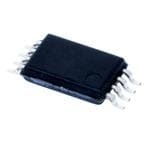
| 描述 | IC OPAMP GP 700KHZ 8TSSOP运算放大器 - 运放 AutoCatDualGeneral Pur+eOpAmp |
| 产品分类 | Linear - Amplifiers - Instrumentation, OP Amps, Buffer Amps集成电路 - IC |
| 品牌 | Texas Instruments |
| 产品手册 | http://www.ti.com/litv/slos414f |
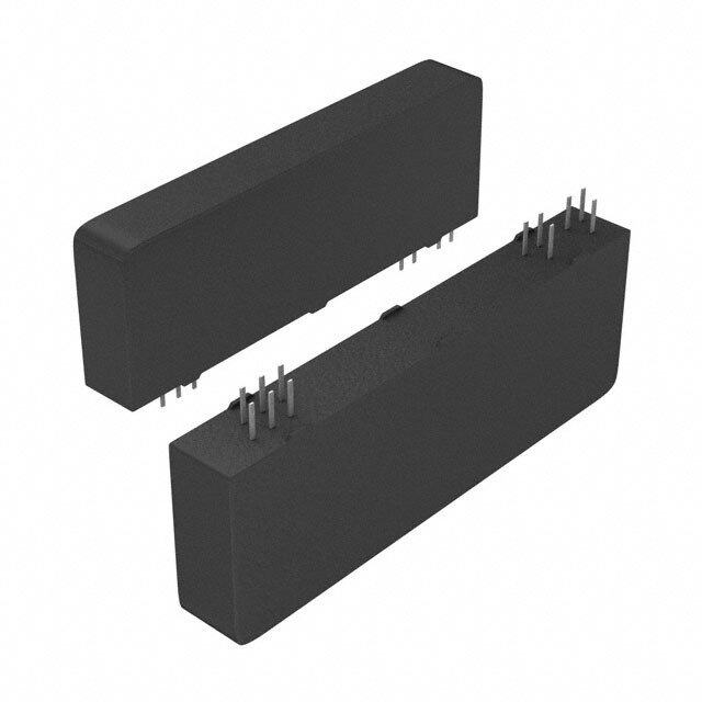
| 产品图片 |
|
| rohs | 过渡期间库存产品核实请求 / 库存产品核实请求 |
| 产品系列 | 放大器 IC,运算放大器 - 运放,Texas Instruments LM2904VQPWRQ1- |
| 数据手册 | |
| 产品型号 | LM2904VQPWRQ1 |
| 产品种类 | Amplifiers - Operational |
| 供应商器件封装 | 8-TSSOP |
| 共模抑制比—最小值 | 65 dB |
| 关闭 | No Shutdown |
| 其它名称 | 296-19590-1 |
| 包装 | 剪切带 (CT) |
| 单位重量 | 34.500 mg |
| 压摆率 | 0.3 V/µs |
| 商标 | Texas Instruments |
| 增益带宽生成 | 0.7 MHz |
| 增益带宽积 | 700kHz |
| 安装类型 | 表面贴装 |
| 安装风格 | SMD/SMT |
| 封装 | Reel |
| 封装/外壳 | 8-TSSOP(0.173",4.40mm 宽) |
| 封装/箱体 | TSSOP-8 |
| 工作温度 | -40°C ~ 125°C |
| 工作电源电压 | 3 V to 32 V, +/- 1.5 V to +/- 16 V |
| 工厂包装数量 | 2000 |
| 技术 | Bipolar |
| 放大器类型 | 通用 |
| 最大双重电源电压 | +/- 16 V |
| 最大工作温度 | + 125 C |
| 最小双重电源电压 | +/- 1.5 V |
| 最小工作温度 | - 40 C |
| 标准包装 | 1 |
| 电压-电源,单/双 (±) | 3 V ~ 26 V, ±1.5 V ~ 13 V |
| 电压-输入失调 | 3mV |
| 电流-电源 | 1mA |
| 电流-输入偏置 | 20nA |
| 电流-输出/通道 | 30mA |
| 电源电流 | 1.2 mA |
| 电路数 | 2 |
| 系列 | LM2904-Q1 |
| 转换速度 | 0.3 V/us |
| 输入偏压电流—最大 | 250 nA |
| 输入参考电压噪声 | 40 nV |
| 输入补偿电压 | 7 mV |
| 输出电流 | 30 mA |
| 输出类型 | - |
| 通道数量 | 2 Channel |


- 商务部:美国ITC正式对集成电路等产品启动337调查
- 曝三星4nm工艺存在良率问题 高通将骁龙8 Gen1或转产台积电
- 太阳诱电将投资9.5亿元在常州建新厂生产MLCC 预计2023年完工
- 英特尔发布欧洲新工厂建设计划 深化IDM 2.0 战略
- 台积电先进制程称霸业界 有大客户加持明年业绩稳了
- 达到5530亿美元!SIA预计今年全球半导体销售额将创下新高
- 英特尔拟将自动驾驶子公司Mobileye上市 估值或超500亿美元
- 三星加码芯片和SET,合并消费电子和移动部门,撤换高东真等 CEO
- 三星电子宣布重大人事变动 还合并消费电子和移动部门
- 海关总署:前11个月进口集成电路产品价值2.52万亿元 增长14.8%


PDF Datasheet 数据手册内容提取
Product Order Technical Tools & Support & Folder Now Documents Software Community LM2904-Q1,LM2904B-Q1 SLOS414H–MAY2003–REVISEDDECEMBER2019 LM2904-Q1, LM2904B-Q1 Industry-Standard Dual Operational Amplifiers for Automotive Applications 1 Features 3 Description • AECQ-100qualifiedforautomotiveapplications The LM2904-Q1 and LM2904B-Q1 are industry- 1 standard operational amplifiers that have been – Temperaturegrade1: –40°Cto+125°C qualified for automotive use in accordance to the – DeviceHBMESDclassification2 AEC-Q100 specifications. The LM2904B-Q1 is the – DeviceCDMESDclassificationC5 next-generation version of the LM2904-Q1, which include two high-voltage (36 V) operational amplifiers • Widesupplyrangeof3Vto36V(LM2904B-Q1) (op amps). The LM2904B-Q1 provides outstanding • Supply-currentof300µAperchannel(LM2904B- value for cost-sensitive applications, with features Q1,typical) including low offset (1 mV, typical), common-mode • Unity-gainbandwidthof1.2MHz(LM2904B-Q1) input range to ground, and high differential input voltagecapability. • Common-modeinputvoltagerangeincludes ground,enablingdirectsensingnearground The LM2904B-Q1 simplifies circuit design with enhanced features such as unity-gain stability, lower • Lowinputoffsetvoltageof3mVat25°C offset voltage of 1 mV (typical), and lower quiescent (LM2904B-Q1,maximum) current of 300 µA (typical). High ESD (2 kV, HBM) • InternalRFandEMIfilter(LM2904B-Q1) and integrated EMI and RF filters enable the LM2904B-Q1 devices to be used in the most rugged, 2 Applications environmentally challenging applications for the automotivemarketplace. • Automotivelighting • Bodyelectronics DeviceInformation(1) • Automotiveheadunit PARTNUMBER PACKAGE BODYSIZE(NOM) • Telematicscontrolunit SOIC(8) 4.90mm×3.90mm • Emergencycall(eCall) LM2904B-Q1 TSSOP(8)(2) 3.00mm×4.40mm • Passivesafety:brakesystem SOT-23(8)(2) 1.60mm×2.90mm • Electricvehicle/hybridelectric: SOIC(8) 4.90mm×3.90mm LM2904-Q1 – Inverterandmotorcontrol TSSOP(8) 3.00mm×4.40mm – On-board(OBC)andwirelesscharger (1) For all available packages, see the orderable addendum at theendofthedatasheet. – Batterymanagementsystem(BMS) (2) Thispackageispreviewonly. Single-Pole,Low-PassFilter R R G F R V 1 OUT V IN C 1 1 f = -3dB 2pR C 1 1 VOUT ( RF (( 1 ( = 1 + V R 1 + sR C IN G 1 1 1 An IMPORTANT NOTICE at the end of this data sheet addresses availability, warranty, changes, use in safety-critical applications, intellectualpropertymattersandotherimportantdisclaimers.PRODUCTIONDATA.
LM2904-Q1,LM2904B-Q1 SLOS414H–MAY2003–REVISEDDECEMBER2019 www.ti.com Table of Contents 1 Features.................................................................. 1 9.3 FeatureDescription.................................................18 2 Applications........................................................... 1 9.4 DeviceFunctionalModes........................................18 3 Description............................................................. 1 10 ApplicationandImplementation........................ 19 4 RevisionHistory..................................................... 2 10.1 ApplicationInformation..........................................19 10.2 TypicalApplication................................................19 5 DeviceComparisonTable..................................... 3 11 PowerSupplyRecommendations..................... 21 6 PinConfigurationandFunctions......................... 4 12 Layout................................................................... 21 7 Specifications......................................................... 5 12.1 LayoutGuidelines.................................................21 7.1 AbsoluteMaximumRatings......................................5 12.2 LayoutExamples...................................................22 7.2 ESDRatings..............................................................5 13 DeviceandDocumentationSupport................. 23 7.3 RecommendedOperatingConditions.......................6 7.4 ThermalInformation..................................................6 13.1 DocumentationSupport........................................23 7.5 ElectricalCharacteristics:LM2904B-Q1...................7 13.2 RelatedLinks........................................................23 7.6 ElectricalCharacteristics:LM2904-Q1,LM2904AV- 13.3 ReceivingNotificationofDocumentationUpdates23 Q1,LM2904V-Q1.......................................................8 13.4 CommunityResources..........................................23 7.7 TypicalCharacteristics..............................................9 13.5 Trademarks...........................................................23 8 ParameterMeasurementInformation................16 13.6 ElectrostaticDischargeCaution............................23 9 DetailedDescription............................................ 17 13.7 Glossary................................................................23 9.1 Overview.................................................................17 14 Mechanical,Packaging,andOrderable Information........................................................... 24 9.2 FunctionalBlockDiagram.......................................17 4 Revision History NOTE:Pagenumbersforpreviousrevisionsmaydifferfrompagenumbersinthecurrentversion. ChangesfromRevisionG(February2019)toRevisionH Page • AddedinformationonSOT23-8packagetoDeviceInformationtable................................................................................... 1 • AddedinformationonSOT23-8packagetotheDeviceComparisonTable.......................................................................... 3 • AddedtheTypicalCharacteristicssectionfortheLM2904B-Q1device................................................................................ 9 • AddedtestcircuitforTHD+Nandsmall-signalstepresponse,G=–1intheParameterMeasurementInformation section.................................................................................................................................................................................. 16 • ChangedspecificvoltagestoaRecommendedOperatingConditionsreference................................................................ 17 • ChangedthefunctionalblockdiagramforLM2904B-Q1intheDetailedDescriptionsection.............................................. 17 ChangesfromRevisionF(April2008)toRevisionG Page • AddedApplicationssection,ESDRatingstable,FeatureDescriptionsection,DeviceFunctionalModes,Application andImplementationsection,PowerSupplyRecommendationssection,Layoutsection,DeviceandDocumentation Supportsection,andMechanical,Packaging,andOrderableInformationsection ............................................................... 1 • Addednewdevicetodatasheet............................................................................................................................................ 1 • AddedAEC-Q100qualificationstatement.............................................................................................................................. 1 2 SubmitDocumentationFeedback Copyright©2003–2019,TexasInstrumentsIncorporated ProductFolderLinks:LM2904-Q1 LM2904B-Q1
LM2904-Q1,LM2904B-Q1 www.ti.com SLOS414H–MAY2003–REVISEDDECEMBER2019 5 Device Comparison Table AMBIENT PARTNUMBER SUPPLY TEMPERATURE VOS IQ/CH INTEGRATEDEMI PACKAGE VOLTAGE (MAXIMUMAT25°C) (TYPICALAT25°C) FILTER RANGE LM2904B-Q1 3Vto36V –40°Cto125°C 3mV 300µA Yes D,DDF(1),PW(1) LM2904-Q1 3Vto26V –40°Cto125°C 7mV 350µA No D,PW LM2904V-Q1 3Vto32V –40°Cto125°C 7mV 350µA No D,PW LM2904AV-Q1 3Vto32V –40°Cto125°C 2mV 350µA No D,PW (1) Packagesforthisdevicearepreviewonly. Copyright©2003–2019,TexasInstrumentsIncorporated SubmitDocumentationFeedback 3 ProductFolderLinks:LM2904-Q1 LM2904B-Q1
LM2904-Q1,LM2904B-Q1 SLOS414H–MAY2003–REVISEDDECEMBER2019 www.ti.com 6 Pin Configuration and Functions D,DDF(1),andPW(1)Packages 8-PinSOIC,SOT23-8,andTSSOP TopView OUT1 1 8 V+ IN1– 2 7 OUT2 IN1+ 3 6 IN2– V– 4 5 IN2+ Not to scale (1) Packageispreviewonly. PinFunctions PIN I/O DESCRIPTION NAME SOIC,SOT23-8,andTSSOP(1) IN1– 2 I Negativeinput IN1+ 3 I Positiveinput IN2– 6 I Negativeinput IN2+ 5 I Positiveinput OUT1 1 O Output OUT2 7 O Output V– 4 — Negative(lowest)supplyorground(forsingle-supplyoperation) V+ 8 — Positive(highest)supply (1) Foralistingofwhichdevicesareavailableinwhatpackages,seetheDeviceComparisonTablesection. 4 SubmitDocumentationFeedback Copyright©2003–2019,TexasInstrumentsIncorporated ProductFolderLinks:LM2904-Q1 LM2904B-Q1
LM2904-Q1,LM2904B-Q1 www.ti.com SLOS414H–MAY2003–REVISEDDECEMBER2019 7 Specifications 7.1 Absolute Maximum Ratings overoperatingambienttemperaturerange(unlessotherwisenoted)(1) MIN MAX UNIT LM2904B-Q1 40 Supplyvoltage,V =([V+]–[V–]) LM2904V-Q1,LM2904AV-Q1 32 V S LM2904-Q1 26 LM2904B-Q1,LM2904V-Q1, –32 32 Differentialinputvoltage,V (2) LM2904AV-Q1 V ID LM2904-Q1 –26 26 LM2904B-Q1 –0.3 40 Inputvoltage,V Eitherinput LM2904V-Q1,LM2904AV-Q1 –0.3 32 V I LM2904-Q1 –0.3 26 Durationofoutputshortcircuit(oneamplifier)toV–at(orbelow)T =25°C, V ≤15V(3) A Unlimited s S Operatingambienttemperature,T –40 125 °C A Operatingvirtual-junctiontemperature,T 150 °C J Storagetemperature,T –65 150 °C stg (1) StressesbeyondthoselistedunderAbsoluteMaximumRatingsmaycausepermanentdamagetothedevice.Thesearestressratings only,anddonotimplyfunctionaloperationofthedeviceattheseoranyotherconditionsbeyondthoseindicatedunderRecommended OperatingConditions.Exposuretoabsolute-maximum-ratedconditionsforextendedperiodsmayaffectdevicereliability. (2) DifferentialvoltagesareatIN+,withrespecttoIN−. (3) Shortcircuitsfromoutputstothesupplypinscancauseexcessiveheatingandeventualdestruction. 7.2 ESD Ratings VALUE UNIT LM2904B-Q1 Human-bodymodel(HBM),perAECQ100-002(1) ±2000 V Electrostaticdischarge V (ESD) Charged-devicemodel(CDM),perAECQ100-011 ±750 LM2904-Q1,LM2904AV-Q1,ANDLM2904V-Q1 Human-bodymodel(HBM),perAECQ100-002(1) ±1000 V Electrostaticdischarge V (ESD) Charged-devicemodel(CDM),perAECQ100-011 ±500 (1) AECQ100-002indicatesthatHBMstressingshallbeinaccordancewiththeANSI/ESDA/JEDECJS-001specification. Copyright©2003–2019,TexasInstrumentsIncorporated SubmitDocumentationFeedback 5 ProductFolderLinks:LM2904-Q1 LM2904B-Q1
LM2904-Q1,LM2904B-Q1 SLOS414H–MAY2003–REVISEDDECEMBER2019 www.ti.com 7.3 Recommended Operating Conditions overoperatingambienttemperaturerange(unlessotherwisenoted) MIN MAX UNIT LM2904B-Q1 3 36 V Supplyvoltage,V =([V+]–[V–]) LM2904AV-Q1,LM2904V-Q1 3 30 V S S LM2904-Q1 3 26 V Common-modevoltage V– (V+)–2 V CM T Operatingambienttemperature –40 125 °C A 7.4 Thermal Information LM2904-Q1,LM2904AV-Q1,LM2904B- Q1,LM2904V-Q1(2) THERMALMETRIC(1) UNIT D(SOIC) PW(TSSOP) 8PINS 8PINS RθJA Junction-to-ambientthermalresistance 124.7 171.7 °C/W RθJC(top) Junction-to-case(top)thermalresistance 66.9 68.8 °C/W RθJB Junction-to-boardthermalresistance 67.9 99.2 °C/W ψJT Junction-to-topcharacterizationparameter 19.2 11.5 °C/W ψJB Junction-to-boardcharacterizationparameter 67.2 97.9 °C/W (1) Formoreinformationabouttraditionalandnewthermalmetrics,seeSemiconductorandICPackageThermalMetrics. (2) Foralistingofwhichdevicesareavailableinwhatpackages,seeDeviceComparisonTable. 6 SubmitDocumentationFeedback Copyright©2003–2019,TexasInstrumentsIncorporated ProductFolderLinks:LM2904-Q1 LM2904B-Q1
LM2904-Q1,LM2904B-Q1 www.ti.com SLOS414H–MAY2003–REVISEDDECEMBER2019 7.5 Electrical Characteristics: LM2904B-Q1 V =(V+)–(V–)=5V–36V(±2.5V–±18V),T =25°C,V =V =V /2,R =10kconnectedtoV /2 S A CM OUT S L S (unlessotherwisenoted) PARAMETER TESTCONDITIONS MIN TYP MAX UNIT OFFSETVOLTAGE ±0.3 ±3.0 VOS Inputoffsetvoltage LM2904B-Q1 TA=–40°Cto+125°C ±4 mV dVOS/dT Inputoffsetvoltagedrift TA=–40°Cto+125°C(1) ±3.5 12 µV/°C PSRR Powersupplyrejectionratio ±2 15 µV/V Channelseparation,dc f=1kHzto20kHz ±1 µV/V INPUTVOLTAGERANGE VCM Common-modevoltagerange VVSS==35VVttoo3366VV TA=–40°Cto+125°C ((VV––)) (V(+V)+–)–1.52 V CMRR Common-moderejectionratio (V–)≤VCM≤(V+)–1.5V VS=3Vto36V 20 100 µV/V (V–)≤VCM≤(V+)–2.0V VS=5Vto36V TA=–40°Cto+125°C 25 316 INPUTBIASCURRENT ±10 ±35 IB Inputbiascurrent TA=–40°Cto+125°C(1) ±50 nA 0.5 4 IOS Inputoffsetcurrent TA=–40°Cto+125°C(1) 5 nA dIOS/dT Inputoffsetcurrentdrift TA=–40°Cto+125°C 10 pA/℃ NOISE En Inputvoltagenoise f=0.1to10Hz 3 µVPP en Inputvoltagenoisedensity f=1kHz 40 nV/√/Hz INPUTIMPEDANCE ZID Differential 10||0.1 MΩ||pF ZIC Common-mode 4||1.5 GΩ||pF OPEN-LOOPGAIN 70 140 AOL Open-loopvoltagegain VS=15V;VO=1Vto11V;RL≥10kΩ,connectedto(V–) TA=–40°Cto+125°C 35 V/mV FREQUENCYRESPONSE GBW Gainbandwidthproduct 1.2 MHz SR Slewrate G=+1 0.5 V/µs Θm Phasemargin G=+1,RL=10kΩ,CL=20pF 56 ° tOR Overloadrecoverytime VIN×gain>VS 10 µs ts Settlingtime To0.1%,VS=5V,2-Vstep,G=+1,CL=100pF 4 µs THD+N Totalharmonicdistortion+noise G=+1,f=1kHz,VO=3.53VRMS,VS=36V,RL=100k,IOUT≤±50µA,BW=80kHz 0.001% OUTPUT IOUT=50µA 1.35 1.42 Positiverail(V+) IOUT=1mA 1.4 1.48 V VO Voltageoutputswingfromrail IIOOUUTT==550mµAA(1) 110.05 11.5601 mV Negativerail(V–) IOUT=1mA 0.75 1 V VS=5V,RL≤10kΩconnectedto(V–) TA=–40°Cto+125°C 5 20 mV VS=15V;VO=V–; Source(1) –20 –30 VID=1V TA=–40°Cto+125°C –10 mA IO Outputcurrent VS=15V;VO=V+; Sink(1) 10 20 VID=–1V TA=–40°Cto+125°C 5 VID=–1V;VO=(V–)+200mV 60 100 μA ISC Short-circuitcurrent VS=20V,(V+)=10V,(V–)=–10V,VO=0V ±40 ±60 mA CLOAD Capacitiveloaddrive 100 pF RO Open-loopoutputresistance f=1MHz,IO=0A 300 Ω POWERSUPPLY IQ Quiescentcurrentperamplifier VVSS==536VV;;IOIO==00AA TA=–40°Cto+125°C 300 486000 µA (1) Specifiedbycharacterizationonly. Copyright©2003–2019,TexasInstrumentsIncorporated SubmitDocumentationFeedback 7 ProductFolderLinks:LM2904-Q1 LM2904B-Q1
LM2904-Q1,LM2904B-Q1 SLOS414H–MAY2003–REVISEDDECEMBER2019 www.ti.com 7.6 Electrical Characteristics: LM2904-Q1, LM2904AV-Q1, LM2904V-Q1 ForV =(V+)–(V–)=5V,T =25°C,R =10kΩconnectedtoV–(unlessotherwisenoted) S A L PARAMETER TESTCONDITIONS(1) MIN TYP MAX UNIT OFFSETVOLTAGE LM2904-Q1, ±3 ±7 VOS Inputoffsetvoltage VVSCM==50VVto;VmOa=xi1m.4umV; LM2904V-A1 TA=–40°Cto125°C ±1 ±1±20 mV LM2904AV-Q1 TA=–40°Cto125°C ±4 dVOS/dT Inputoffsetvoltagedrift TA=–40°Cto125°C ±7 µV/°C Inputoffsetvoltagevspowersupply PSRR (ΔVIO/ΔVS) VS=5Vto30V 65 100 dB VO1/VO2 Channelseparation f=1kHzto20kHz 120 dB INPUTVOLTAGERANGE (V–) (V+)–1.5 VCM Common-modevoltagerange VS=5Vtomaximum TA=–40°Cto125°C (V–) (V+)–2 V CMRR Common-moderejectionratio VS=5Vtomaximum;VCM=0V 65 80 dB INPUTBIASCURRENT –20 –250 IB Inputbiascurrent VO=(V–)+1.4V TA=–40°Cto125°C –500 nA 2 50 LM2904-Q1 IOS Inputoffsetcurrent VO=(V–)+1.4V LM2904AV-Q1, TA=–40°Cto125°C 2 35000 nA LM2904V-Q1 TA=–40°Cto125°C 150 dIOS/dT Inputoffsetcurrentdrift TA=–40°Cto125°C 10 pA/°C NOISE en Inputvoltagenoisedensity f=1kHz 40 nV/√Hz OPEN-LOOPGAIN AOL Open-loopvoltagegain VcoSn=ne1c5teVd;tVoO(V=–()V–)+1Vto(V–)+11V;RL≥2kΩ, TA=–40°Cto125°C 2155 100 V/mV FREQUENCYRESPONSE GBW Gainbandwidthproduct 0.7 MHz SR Slewrate G=+1 0.3 V/µs OUTPUT RL≥10kΩ VS–1.5 VS=maximum; 4 LM2904-Q1 RL=2kΩ VS=maximum; 3 2 VO Voltageoutputswingfromrail Positiverail RVSL≥=1m0akxΩimum; TA=–40°Cto125°C 6 V LM2904AV-Q1, RL=2kΩ LM2904V-Q1 VS=maximum; 5 4 RL≥10kΩ Negativerail VRSL≤=150Vk;Ω TA=–40°Cto125°C 5 20 mV –20 –30 VS=15V;VO=V–;VID=1V Source TA=–40°Cto125°C –10 mA IO Outputcurrent VVSID==1–51VV;VO=V+; Sink TA=–40°Cto125°C 150 20 LM2904-Q1 30 VID=–1V;VO=(V–)+200mV LM2904AV-Q1,LM2904V-Q1 12 40 µA ISC Short-circuitcurrent VS=10V;VO=VS/2 ±40 ±60 mA POWERSUPPLY IQ Quiescentcurrentperamplifier VVOS==mVSax/i2m;uIOm=;V0OA=maximum/2;IO=0A TA=–40°Cto125°C 355000 1060000 µA (1) Allcharacteristicsaremeasuredwithzerocommon-modeinputvoltage,unlessotherwisespecified.MaximumV fortestingpurposesis S 26VforLM2904-Q1and32VforLM2904AV-Q1/LM2904V-Q1. 8 SubmitDocumentationFeedback Copyright©2003–2019,TexasInstrumentsIncorporated ProductFolderLinks:LM2904-Q1 LM2904B-Q1
LM2904-Q1,LM2904B-Q1 www.ti.com SLOS414H–MAY2003–REVISEDDECEMBER2019 7.7 Typical Characteristics TypicalcharacteristicssectionisapplicableforLM2904B-Q1.ThetypicalcharacteristicsdatasectionwastakenwithT = A 25°C,V =36V(±18V),V =V /2,R =10kΩconnectedtoV /2(unlessotherwisenoted). S CM S LOAD S 20 30 18 27 16 24 14 21 %) 12 %) 18 s ( s ( er 10 er 15 plifi plifi m 8 m 12 A A 6 9 4 6 2 3 0 0 -1800 -1200 -600 0 600 1200 1800 0 0.25 0.5 0.75 1 1.25 1.5 1.75 2 2.25 2.5 2.75 Offset Voltage (µV) DC11 Offset Voltage Drift (µV/°C) DC12 Figure1.OffsetVoltageProductionDistribution Figure2.OffsetVoltageDriftDistribution 750 500 450 300 V) V) µ µ e ( 150 e ( 100 g g a a olt olt V V et -150 et -100 s s Off Off -450 -300 -750 -500 -40 -20 0 20 40 60 80 100 120 -18 -12 -6 0 6 12 17 Temperature (°C) Common-Mode Voltage (V) DC10 DC10 Figure3.OffsetVoltagevsTemperature Figure4.OffsetVoltagevsCommon-ModeVoltage 90 100 70 G = 1 80 90 60 G = 10 Gain (dB) 567000 678000 Gain (dB) 4500 GGG === 11–001000 Open Loop Voltage 123400000 1234500000 (cid:1)Phase () Closed Lopp Voltage -112300000 -10 Gain (dB) 0 -20 Phase (°) -20 -10 -30 1k 10k 100k 1M 1k 10k 100k 1M Frequency (Hz) Frequency (Hz) D012 D017 Figure5.Open-LoopGainandPhasevsFrequency Figure6.Closed-LoopGainvsFrequency Copyright©2003–2019,TexasInstrumentsIncorporated SubmitDocumentationFeedback 9 ProductFolderLinks:LM2904-Q1 LM2904B-Q1
LM2904-Q1,LM2904B-Q1 SLOS414H–MAY2003–REVISEDDECEMBER2019 www.ti.com Typical Characteristics (continued) TypicalcharacteristicssectionisapplicableforLM2904B-Q1.ThetypicalcharacteristicsdatasectionwastakenwithT = A 25°C,V =36V(±18V),V =V /2,R =10kΩconnectedtoV /2(unlessotherwisenoted). S CM S LOAD S -5 120 IB+ IB– 100 A) -7.5 A) 80 Current (n -10 Current (p 4600 s et a s put Bi ut Off 20 In -12.5 np 0 I -20 -15 -40 -20 -15 -10 -5 0 5 10 15 20 -20 -15 -10 -5 0 5 10 15 20 Common-Mode Voltage (V) Common-Mode Voltage (V) DC3I DC3I Figure7.InputBiasCurrentvsCommon-ModeVoltage Figure8.InputOffsetCurrentvsCommon-ModeVoltage -6 0.06 -7 0.045 A) nA) nt (n -8 ent ( 0.03 as Curre -9 set Curr 0.015 Bi IB+ Off Input -10 IB– Input 0 -11 -0.015 -12 -0.03 -40 -10 20 50 80 110 130 -40 -10 20 50 80 110 130 Temperature (°C) Temperature (°C) DCIB DCIO Figure9.InputBiasCurrentvsTemperature Figure10.InputOffsetCurrentvsTemperature V+ (V–) + 18 V –40(cid:1)C 25(cid:1)C (V–) + 15 V 125(cid:1)C (V+) – 3 V V) V)(V–) + 12 V e ( e ( g g a a olt (V+) – 6 V olt (V–) + 9 V V V ut ut p p ut ut (V–) + 6 V O O (V+) – 9 V –40(cid:1)C (V–) + 3 V 25(cid:1)C 125(cid:1)C (V+) – 12 V V– 0 10 20 30 40 50 0 5 10 15 20 25 30 35 40 Output Current (mA) Output Current (mA) DC13 DC1- Figure11.OutputVoltageSwingvs Figure12.OutputVoltageSwingvs OutputCurrent(Sourcing) OutputCurrent(Sinking) 10 SubmitDocumentationFeedback Copyright©2003–2019,TexasInstrumentsIncorporated ProductFolderLinks:LM2904-Q1 LM2904B-Q1
LM2904-Q1,LM2904B-Q1 www.ti.com SLOS414H–MAY2003–REVISEDDECEMBER2019 Typical Characteristics (continued) TypicalcharacteristicssectionisapplicableforLM2904B-Q1.ThetypicalcharacteristicsdatasectionwastakenwithT = A 25°C,V =36V(±18V),V =V /2,R =10kΩconnectedtoV /2(unlessotherwisenoted). S CM S LOAD S 100 120 PSRR+ 90 PSRR- dB) 115 80 CMRR o ( R (dB) 70 on Rati 110 MR 60 ecti 105 C 50 ej nd e R 100 a 40 d SRR 30 n-Mo 95 P o 20 mm 10 Co 90 VS= 36V VS= 5V 0 85 1k 10k 100k 1M -40 -10 20 50 80 110 130 Frequency (Hz) D001 Temperature (°C) DC2_ Figure13.CMRRandPSRRvsFrequency Figure14.Common-ModeRejectionRatiovs Temperature(dB) -118 1.6 B) 1.2 d o ( -119 0.8 ati R 0.4 on -120 V) ejecti ge (µ 0 R a -0.4 y -121 olt pl V p -0.8 u S wer -122 -1.2 o P -1.6 -123 -2 -40 -20 0 20 40 60 80 100 120 140 0 1 2 3 4 5 6 7 8 9 10 Temperature (°C) Time (s) DC8_ D011 V =5Vto36V S Figure15.PowerSupplyRejectionRatiovs Figure16.0.1-Hzto10-HzNoise Temperature(dB) 100 -32 Hz) 90 -40 120 k (cid:1)k(cid:1) (cid:151) nV/ 80 -48 sity ( 70 -56 Den 60 dB) -64 ectral 50 D+N ( -72 Sp 40 TH -80 se 30 -88 oi N e 20 -96 g olta 10 -104 V 0 -112 10 100 1k 10k 100k 100 1k 10k Frequency (Hz) D010 Frequency (Hz) D013 G=1,f=1kHz,BW=80kHz, V =10V ,R connectedtoV– OUT PP L Figure17.InputVoltageNoiseSpectralDensityvs Figure18.THD+NRatiovsFrequency,G=1 Frequency Copyright©2003–2019,TexasInstrumentsIncorporated SubmitDocumentationFeedback 11 ProductFolderLinks:LM2904-Q1 LM2904B-Q1
LM2904-Q1,LM2904B-Q1 SLOS414H–MAY2003–REVISEDDECEMBER2019 www.ti.com Typical Characteristics (continued) TypicalcharacteristicssectionisapplicableforLM2904B-Q1.ThetypicalcharacteristicsdatasectionwastakenwithT = A 25°C,V =36V(±18V),V =V /2,R =10kΩconnectedtoV /2(unlessotherwisenoted). S CM S LOAD S -32 -30 10 k(cid:1) -40 2 k(cid:1) -40 -48 -50 -56 -60 B) B) N (d -64 N (d -70 + + D -72 D -80 H H T T -80 -90 -88 -100 -96 -110 10 k(cid:1) 2 k(cid:1) -104 -120 100 1k 10k 0.001 0.01 0.1 1 10 2200 Frequency (Hz) D014 Amplitude (VPP) D015 G=–1,f=1kHz,BW=80kHz, G=1,f=1kHz,BW=80kHz, V =10V ,R connectedtoV– R connectedtoV– OUT PP L L Figure19.THD+NRatiovsFrequency,G=–1 Figure20.THD+NvsOutputAmplitude,G=1 -20 460 -35 430 A) µ N (dB) --6550 Current ( 347000 D+ nt H e T -80 esc 340 ui Q -95 310 10 k(cid:1) 2 k(cid:1) -110 280 0.001 0.01 0.1 1 10 2200 3 9 15 21 27 33 36 Amplitude (VPP) D016 Supply Voltage (V) DC_S G=–1,f=1kHz,BW=80kHz, R connectedtoV– L Figure21.THD+NvsOutputAmplitude,G=–1 Figure22.QuiescentCurrentvsSupplyVoltage 600 500 VS= 36V mplifier (µA) 458400 VS= 5V (cid:1)edance () 400 A p nt per 420 put Im 300 Curre 360 p Out ent Loo 200 uiesc 300 Open Q 240 100 -40 -20 0 20 40 60 80 100 120 1k 10k 100k 1M Temperature (°C) Frequency (Hz) DC4_ D006 Figure23.QuiescentCurrentvsTemperature Figure24.Open-LoopOutputImpedancevsFrequency 12 SubmitDocumentationFeedback Copyright©2003–2019,TexasInstrumentsIncorporated ProductFolderLinks:LM2904-Q1 LM2904B-Q1
LM2904-Q1,LM2904B-Q1 www.ti.com SLOS414H–MAY2003–REVISEDDECEMBER2019 Typical Characteristics (continued) TypicalcharacteristicssectionisapplicableforLM2904B-Q1.ThetypicalcharacteristicsdatasectionwastakenwithT = A 25°C,V =36V(±18V),V =V /2,R =10kΩconnectedtoV /2(unlessotherwisenoted). S CM S LOAD S 44 18 Overshoot (+) Overshoot (+) 40 Overshoot (-) 16 Overshoot (–) 36 14 32 12 %) %) ot ( 28 ot ( 10 o o h h s 24 s 8 er er v v O 20 O 6 16 4 12 2 8 0 0 40 80 120 160 200 240 280 320 360 40 80 120 160 200 240 280 320 360 Capacitance load (pF) Capacitance load (pF) D019 D020 G=1,100-mVoutputstep,R =open G=–1,100-mVoutputstep,R =open L L Figure25.Small-SignalOvershootvsCapacitiveLoad Figure26.Small-SignalOvershootvsCapacitiveLoad 60 20 Input 57 Output 54 10 51 n (°) 48 V) Margi 45 age ( 0 e olt as 42 V h P 39 -10 36 33 30 -20 0 40 80 120 160 200 240 280 320 360 0 200 400 600 800 1000 Capacitance Load (pF) D018 Time ((cid:1)s) D021 G=–10 Figure27.PhaseMarginvsCapacitiveLoad Figure28.OverloadRecovery 10 10 7.5 7.5 5 5 V) 2.5 V) 2.5 m m e ( 0 e ( 0 g g a a Volt -2.5 Volt -2.5 -5 -5 -7.5 Input -7.5 Input Output Output -10 -10 0 20 40 60 80 100 0 20 40 60 80 100 Time ((cid:1)s) Time ((cid:1)s) D022 D023 G=1,R =open G=–1,R =open,R =10K L L FB Figure29.Small-SignalStepResponse,G=1 Figure30.Small-SignalStepResponse,G=–1 Copyright©2003–2019,TexasInstrumentsIncorporated SubmitDocumentationFeedback 13 ProductFolderLinks:LM2904-Q1 LM2904B-Q1
LM2904-Q1,LM2904B-Q1 SLOS414H–MAY2003–REVISEDDECEMBER2019 www.ti.com Typical Characteristics (continued) TypicalcharacteristicssectionisapplicableforLM2904B-Q1.ThetypicalcharacteristicsdatasectionwastakenwithT = A 25°C,V =36V(±18V),V =V /2,R =10kΩconnectedtoV /2(unlessotherwisenoted). S CM S LOAD S 20 40 V) 16 V) 32 m m e ( 12 e ( 24 u u al 8 al 16 V V al 4 al 8 n n Fi Fi m 0 m 0 o o a fr -4 a fr -8 Delt -8 Delt -16 put -12 put -24 ut ut O -16 O -32 -20 -40 0 0.5 1 1.5 2 2.5 3 3.5 4 4.5 5 0 0.5 1 1.5 2 2.5 3 3.5 4 4.5 5 Time ((cid:1)s) Time ((cid:1)s) D003 D004 G=1,R =open G=1,R =open L L Figure31.Large-SignalStepResponse(Rising) Figure32.Large-SignalStepResponse(Falling) 2.5 0.675 Output Positive 2 Input Negative 1.5 0.625 1 s) Votlage(V) -00..505 ew Rate(V/(cid:2) 00..552755 -1 Sl -1.5 0.475 -2 -2.5 0.425 0 20 40 60 80 100 -40 -25 -10 5 20 35 50 65 80 95 110 125 Time (µs) Temp((cid:1)C) AC_S D009 G=1,R =open L Figure33.Large-SignalStepResponse Figure34.SlewRatevsTemperature 60 15 14 13 A) 40 V)PP 12 nt (m 20 age ( 1101 hort-Circuit Curre -200 SSionukricnigng mum Output Volt 456789 S -40 Maxi 3 2 1 -60 0 -40 -25 -10 5 20 35 50 65 80 95 110 125 1k 10k 100k 1M Temperature (°C) DC7_ Frequency (Hz) D005 V =15V S Figure35.Short-CircuitCurrentvsTemperature Figure36.MaximumOutputVoltagevsFrequency 14 SubmitDocumentationFeedback Copyright©2003–2019,TexasInstrumentsIncorporated ProductFolderLinks:LM2904-Q1 LM2904B-Q1
LM2904-Q1,LM2904B-Q1 www.ti.com SLOS414H–MAY2003–REVISEDDECEMBER2019 Typical Characteristics (continued) TypicalcharacteristicssectionisapplicableforLM2904B-Q1.ThetypicalcharacteristicsdatasectionwastakenwithT = A 25°C,V =36V(±18V),V =V /2,R =10kΩconnectedtoV /2(unlessotherwisenoted). S CM S LOAD S -75 90 84 -85 78 B) d 72 paration ( -1-0955 R (dB) 6606 nnel Se -115 EMIR 4584 a h 42 C -125 36 30 -135 24 1k 10k 100k 1M 1M 10M 100M 1G Frequency (Hz) D008 Frequency (Hz) D007 Figure37.ChannelSeparationvsFrequency Figure38.EMIRR(ElectromagneticInterferenceRejection Ratio)vsFrequency Copyright©2003–2019,TexasInstrumentsIncorporated SubmitDocumentationFeedback 15 ProductFolderLinks:LM2904-Q1 LM2904B-Q1
LM2904-Q1,LM2904B-Q1 SLOS414H–MAY2003–REVISEDDECEMBER2019 www.ti.com 8 Parameter Measurement Information V CC+ − V O V + I VCC− CL RL Figure39.Unity-GainAmplifier 900Ω V CC+ 100Ω V = 0 V − I RS VO + V CC− Figure40.Noise-TestCircuit 10 k (cid:1) +18V – V IN + -18V RL GND GND Figure41.TestCircuit,G= –1,forTHD+NandSmall-SignalStepResponse 16 SubmitDocumentationFeedback Copyright©2003–2019,TexasInstrumentsIncorporated ProductFolderLinks:LM2904-Q1 LM2904B-Q1
LM2904-Q1,LM2904B-Q1 www.ti.com SLOS414H–MAY2003–REVISEDDECEMBER2019 9 Detailed Description 9.1 Overview The LM2904-Q1 and LM2904B-Q1 devices consist of two independent, high-gain frequency-compensated operational amplifiers designed to operate from a single supply over a wide range of voltages. Operation from split supplies also is possible if the difference between the two supplies is within the supply voltage range specified in the Recommended Operating Conditions section, and V is at least 1.5 V more positive than the S inputcommon-modevoltage.Thelowsupply-currentdrainisindependentofthemagnitudeofthesupplyvoltage. Applications include transducer amplifiers, dc amplification blocks, and all the conventional operational amplifier circuits that now can be implemented more easily in single-supply-voltage systems. For example, these devices canbeoperateddirectlyfromthestandard5-Vsupplyusedindigitalsystemsandeasilycan provide the required interfaceelectronicswithoutadditional ±5-Vsupplies. 9.2 Functional Block Diagram VCC+ ~6 µA ~6 µA ~100 µA Current Current Current Regulator Regulator Regulator IN- OUT IN+ ~120 µA Current Regulator Copyright©2003–2019,TexasInstrumentsIncorporated SubmitDocumentationFeedback 17 ProductFolderLinks:LM2904-Q1 LM2904B-Q1
LM2904-Q1,LM2904B-Q1 SLOS414H–MAY2003–REVISEDDECEMBER2019 www.ti.com 9.3 Feature Description 9.3.1 Unity-GainBandwidth The unity-gain bandwidth is the frequency up to which an amplifier with a unity gain may be operated without greatlydistortingthesignal.Thesedeviceshavea1.2-MHzunity-gainbandwidth(LM2904B-Q1). 9.3.2 SlewRate The slew rate is the rate at which an operational amplifier can change its output when there is a change on the input.Thesedeviceshavea0.5-V/µsslewrate(LM2904B-Q1). 9.3.3 InputCommonModeRange The valid common mode range is from device ground to V – 1.5 V (V – 2 V across temperature). Inputs may S S exceed V up to the maximum V without device damage. At least one input must be in the valid input common- S S moderangefortheoutputtobethecorrectphase.Ifbothinputsexceedthe valid range, then the output phase is undefined. If either input more than 0.3 V below V– then input current should be limited to 1 mA and the output phaseisundefined. 9.4 Device Functional Modes The LM2904-Q1 and LM2904B-Q1 devices are powered on when the supply is connected. This device can be operatedasasingle-supplyoperationalamplifierordual-supplyamplifier,dependingontheapplication. 18 SubmitDocumentationFeedback Copyright©2003–2019,TexasInstrumentsIncorporated ProductFolderLinks:LM2904-Q1 LM2904B-Q1
LM2904-Q1,LM2904B-Q1 www.ti.com SLOS414H–MAY2003–REVISEDDECEMBER2019 10 Application and Implementation NOTE Information in the following applications sections is not part of the TI component specification, and TI does not warrant its accuracy or completeness. TI’s customers are responsible for determining suitability of components for their purposes. Customers should validateandtesttheirdesignimplementationtoconfirmsystemfunctionality. 10.1 Application Information The LM2904-Q1 and LM2904B-Q1 operational amplifiers are useful in a wide range of signal conditioning applications. Inputs can be powered before V for flexibility in multiple supply circuits. For full application design S guidelines related to this family of devices, please refer to the application report Application design guidelines for LM324/LM358devices. 10.2 Typical Application Atypicalapplicationforanoperationalamplifierisaninvertingamplifier.Thisamplifiertakesapositivevoltageon the input, and makes it a negative voltage of the same magnitude. In the same manner, it also makes negative voltagespositive. RF Vsup+ RI V OUT + V IN Vsup- Figure42. ApplicationSchematic 10.2.1 DesignRequirements The supply voltage must be chosen such that it is larger than the input voltage range and output range. For instance, this application scales a signal of ±0.5 V to ±1.8 V. Setting the supply at ±12 V is sufficient to accommodatethisapplication. 10.2.2 DetailedDesignProcedure DeterminethegainrequiredbytheinvertingamplifierusingEquation1 andEquation2: VOUT A V VIN (1) 1.8 A (cid:16)3.6 V (cid:16)0.5 (2) Once the desired gain is determined, choose a value for R or R . Choosing a value in the kilohm range is I F desirable because the amplifier circuit uses currents in the milliampere range. This ensures the part does not draw too much current. This example uses 10 kΩ for R which means 36 kΩ is used for R . This was determined I F byEquation3. RF A (cid:16) V RI (3) Copyright©2003–2019,TexasInstrumentsIncorporated SubmitDocumentationFeedback 19 ProductFolderLinks:LM2904-Q1 LM2904B-Q1
LM2904-Q1,LM2904B-Q1 SLOS414H–MAY2003–REVISEDDECEMBER2019 www.ti.com Typical Application (continued) 10.2.3 ApplicationCurve 2 VIN 1.5 VOUT 1 0.5 olts0 V -0.5 -1 -1.5 -2 0 0.5 1 1.5 2 Time (ms) Figure43. InputandOutputVoltagesoftheInvertingAmplifier 20 SubmitDocumentationFeedback Copyright©2003–2019,TexasInstrumentsIncorporated ProductFolderLinks:LM2904-Q1 LM2904B-Q1
LM2904-Q1,LM2904B-Q1 www.ti.com SLOS414H–MAY2003–REVISEDDECEMBER2019 11 Power Supply Recommendations CAUTION Supply voltages larger than specified in the recommended operating region can permanentlydamagethedevice(seetheAbsoluteMaximumRatings). Place 0.1-µF bypass capacitors close to the power-supply pins to reduce errors coupling in from noisy or high- impedance power supplies. For more detailed information on bypass capacitor placement, see the Layout section. 12 Layout 12.1 Layout Guidelines Forbestoperationalperformanceofthedevice,usegoodPCBlayoutpractices,including: • Noise can propagate into analog circuitry through the power pins of the circuit as a whole, as well as the operational amplifier. Bypass capacitors are used to reduce the coupled noise by providing low-impedance powersourceslocaltotheanalogcircuitry. – Connect low-ESR, 0.1-µF ceramic bypass capacitors between each supply pin and ground, placed as close to the device as possible. A single bypass capacitor from V+ to ground is applicable for single- supplyapplications. • Separate grounding for analog and digital portions of circuitry is one of the simplest and most-effective methods of noise suppression. One or more layers on multilayer PCBs are usually devoted to ground planes. A ground plane helps distribute heat and reduces EMI noise pickup. Make sure to physically separate digital andanaloggrounds,payingattentiontotheflowofthegroundcurrent. • To reduce parasitic coupling, run the input traces as far away from the supply or output traces as possible. If it is not possible to keep them separate, it is much better to cross the sensitive trace perpendicular as opposedtoinparallelwiththenoisytrace. • Place the external components as close to the device as possible. Keeping R and R close to the inverting F G inputminimizesparasiticcapacitance,asshownintheLayoutExamples section. • Keep the length of input traces as short as possible. Always remember that the input traces are the most sensitivepartofthecircuit. • Consider a driven, low-impedance guard ring around the critical traces. A guard ring can significantly reduce leakagecurrentsfromnearbytracesthatareatdifferentpotentials. Copyright©2003–2019,TexasInstrumentsIncorporated SubmitDocumentationFeedback 21 ProductFolderLinks:LM2904-Q1 LM2904B-Q1
LM2904-Q1,LM2904B-Q1 SLOS414H–MAY2003–REVISEDDECEMBER2019 www.ti.com 12.2 Layout Examples Place components close to device and to each other to reduce parasitic errors Run the input traces as far away from the supply lines VS+ as possible RF OUT1 V+ RG GND IN1(cid:237) OUT2 VIN IN1+ IN2(cid:237) GND RIN V(cid:237) IN2+ Only needed for Use low-ESR, ceramic dual-supply bypass capacitor operation (cid:237) GND VS (or GND for single supply) Ground (GND) plane on another layer Figure44. OperationalAmplifierBoardLayoutforNoninvertingConfiguration RIN VIN + VOUT RG RF Figure45. OperationalAmplifierSchematicforNoninvertingConfiguration 22 SubmitDocumentationFeedback Copyright©2003–2019,TexasInstrumentsIncorporated ProductFolderLinks:LM2904-Q1 LM2904B-Q1
LM2904-Q1,LM2904B-Q1 www.ti.com SLOS414H–MAY2003–REVISEDDECEMBER2019 13 Device and Documentation Support 13.1 Documentation Support 13.1.1 RelatedDocumentation Forrelateddocumentationseethefollowing:TexasInstruments,ApplicationDesignGuidelinesforLM324/LM358 Devicesapplicationreport 13.2 Related Links The table below lists quick access links. Categories include technical documents, support and community resources,toolsandsoftware,andquickaccesstoordernow. Table1.RelatedLinks TECHNICAL TOOLS& SUPPORT& PARTS PRODUCTFOLDER ORDERNOW DOCUMENTS SOFTWARE COMMUNITY LM2904-Q1 Clickhere Clickhere Clickhere Clickhere Clickhere LM2904B-Q1 Clickhere Clickhere Clickhere Clickhere Clickhere 13.3 Receiving Notification of Documentation Updates To receive notification of documentation updates, navigate to the device product folder on ti.com. In the upper right corner, click on Alert me to register and receive a weekly digest of any product information that has changed.Forchangedetails,reviewtherevisionhistoryincludedinanyreviseddocument. 13.4 Community Resources TI E2E™ support forums are an engineer's go-to source for fast, verified answers and design help — straight fromtheexperts.Searchexistinganswersoraskyourownquestiontogetthequickdesignhelpyouneed. Linked content is provided "AS IS" by the respective contributors. They do not constitute TI specifications and do notnecessarilyreflectTI'sviews;seeTI'sTermsofUse. 13.5 Trademarks E2EisatrademarkofTexasInstruments. Allothertrademarksarethepropertyoftheirrespectiveowners. 13.6 Electrostatic Discharge Caution This integrated circuit can be damaged by ESD. Texas Instruments recommends that all integrated circuits be handled with appropriateprecautions.Failuretoobserveproperhandlingandinstallationprocedurescancausedamage. ESDdamagecanrangefromsubtleperformancedegradationtocompletedevicefailure.Precisionintegratedcircuitsmaybemore susceptibletodamagebecauseverysmallparametricchangescouldcausethedevicenottomeetitspublishedspecifications. 13.7 Glossary SLYZ022—TIGlossary. Thisglossarylistsandexplainsterms,acronyms,anddefinitions. Copyright©2003–2019,TexasInstrumentsIncorporated SubmitDocumentationFeedback 23 ProductFolderLinks:LM2904-Q1 LM2904B-Q1
LM2904-Q1,LM2904B-Q1 SLOS414H–MAY2003–REVISEDDECEMBER2019 www.ti.com 14 Mechanical, Packaging, and Orderable Information The following pages include mechanical packaging and orderable information. This information is the most- current data available for the designated devices. This data is subject to change without notice and without revisionofthisdocument.Forbrowserbasedversionsofthisdatasheet,seetheleft-handnavigationpane. 24 SubmitDocumentationFeedback Copyright©2003–2019,TexasInstrumentsIncorporated ProductFolderLinks:LM2904-Q1 LM2904B-Q1
PACKAGE OPTION ADDENDUM www.ti.com 6-Feb-2020 PACKAGING INFORMATION Orderable Device Status Package Type Package Pins Package Eco Plan Lead/Ball Finish MSL Peak Temp Op Temp (°C) Device Marking Samples (1) Drawing Qty (2) (6) (3) (4/5) LM2904AVQDRG4Q1 ACTIVE SOIC D 8 2500 Green (RoHS NIPDAU Level-1-260C-UNLIM -40 to 125 2904AVQ & no Sb/Br) LM2904AVQDRQ1 ACTIVE SOIC D 8 2500 Green (RoHS NIPDAU Level-1-260C-UNLIM -40 to 125 2904AVQ & no Sb/Br) LM2904AVQPWRG4Q1 ACTIVE TSSOP PW 8 2000 Green (RoHS NIPDAU Level-1-260C-UNLIM -40 to 125 2904AVQ & no Sb/Br) LM2904AVQPWRQ1 ACTIVE TSSOP PW 8 2000 Green (RoHS NIPDAU Level-1-260C-UNLIM -40 to 125 2904AVQ & no Sb/Br) LM2904BQDRQ1 ACTIVE SOIC D 8 2500 Green (RoHS NIPDAU Level-2-260C-1 YEAR -40 to 125 2904BQ & no Sb/Br) LM2904BQPWRQ1 PREVIEW TSSOP PW 8 2000 TBD Call TI Call TI -40 to 125 LM2904QDRG4Q1 ACTIVE SOIC D 8 2500 Green (RoHS NIPDAU Level-1-260C-UNLIM -40 to 125 2904Q1 & no Sb/Br) LM2904QDRQ1 ACTIVE SOIC D 8 2500 Green (RoHS NIPDAU Level-1-260C-UNLIM -40 to 125 2904Q1 & no Sb/Br) LM2904QPWRG4Q1 ACTIVE TSSOP PW 8 2000 Green (RoHS NIPDAU Level-1-260C-UNLIM -40 to 125 2904Q1 & no Sb/Br) LM2904QPWRQ1 ACTIVE TSSOP PW 8 2000 Green (RoHS NIPDAU Level-1-260C-UNLIM -40 to 125 2904Q1 & no Sb/Br) LM2904VQDRG4Q1 ACTIVE SOIC D 8 2500 Green (RoHS NIPDAU Level-1-260C-UNLIM -40 to 125 2904VQ & no Sb/Br) LM2904VQDRQ1 ACTIVE SOIC D 8 2500 Green (RoHS NIPDAU Level-1-260C-UNLIM -40 to 125 2904VQ1 & no Sb/Br) LM2904VQPWRG4Q1 ACTIVE TSSOP PW 8 2000 Green (RoHS NIPDAU Level-1-260C-UNLIM 2904VQ & no Sb/Br) LM2904VQPWRQ1 ACTIVE TSSOP PW 8 2000 Green (RoHS NIPDAU Level-1-260C-UNLIM -40 to 125 2904VQ & no Sb/Br) PLM2904BQPWRQ1 ACTIVE TSSOP PW 8 2000 TBD Call TI Call TI -40 to 125 (1) The marketing status values are defined as follows: ACTIVE: Product device recommended for new designs. LIFEBUY: TI has announced that the device will be discontinued, and a lifetime-buy period is in effect. NRND: Not recommended for new designs. Device is in production to support existing customers, but TI does not recommend using this part in a new design. PREVIEW: Device has been announced but is not in production. Samples may or may not be available. OBSOLETE: TI has discontinued the production of the device. Addendum-Page 1
PACKAGE OPTION ADDENDUM www.ti.com 6-Feb-2020 (2) RoHS: TI defines "RoHS" to mean semiconductor products that are compliant with the current EU RoHS requirements for all 10 RoHS substances, including the requirement that RoHS substance do not exceed 0.1% by weight in homogeneous materials. Where designed to be soldered at high temperatures, "RoHS" products are suitable for use in specified lead-free processes. TI may reference these types of products as "Pb-Free". RoHS Exempt: TI defines "RoHS Exempt" to mean products that contain lead but are compliant with EU RoHS pursuant to a specific EU RoHS exemption. Green: TI defines "Green" to mean the content of Chlorine (Cl) and Bromine (Br) based flame retardants meet JS709B low halogen requirements of <=1000ppm threshold. Antimony trioxide based flame retardants must also meet the <=1000ppm threshold requirement. (3) MSL, Peak Temp. - The Moisture Sensitivity Level rating according to the JEDEC industry standard classifications, and peak solder temperature. (4) There may be additional marking, which relates to the logo, the lot trace code information, or the environmental category on the device. (5) Multiple Device Markings will be inside parentheses. Only one Device Marking contained in parentheses and separated by a "~" will appear on a device. If a line is indented then it is a continuation of the previous line and the two combined represent the entire Device Marking for that device. (6) Lead/Ball Finish - Orderable Devices may have multiple material finish options. Finish options are separated by a vertical ruled line. Lead/Ball Finish values may wrap to two lines if the finish value exceeds the maximum column width. Important Information and Disclaimer:The information provided on this page represents TI's knowledge and belief as of the date that it is provided. TI bases its knowledge and belief on information provided by third parties, and makes no representation or warranty as to the accuracy of such information. Efforts are underway to better integrate information from third parties. TI has taken and continues to take reasonable steps to provide representative and accurate information but may not have conducted destructive testing or chemical analysis on incoming materials and chemicals. TI and TI suppliers consider certain information to be proprietary, and thus CAS numbers and other limited information may not be available for release. In no event shall TI's liability arising out of such information exceed the total purchase price of the TI part(s) at issue in this document sold by TI to Customer on an annual basis. OTHER QUALIFIED VERSIONS OF LM2904-Q1, LM2904B-Q1 : •Catalog: LM2904, LM2904B •Enhanced Product: LM2904-EP NOTE: Qualified Version Definitions: •Catalog - TI's standard catalog product •Enhanced Product - Supports Defense, Aerospace and Medical Applications Addendum-Page 2
PACKAGE MATERIALS INFORMATION www.ti.com 10-Dec-2019 TAPE AND REEL INFORMATION *Alldimensionsarenominal Device Package Package Pins SPQ Reel Reel A0 B0 K0 P1 W Pin1 Type Drawing Diameter Width (mm) (mm) (mm) (mm) (mm) Quadrant (mm) W1(mm) LM2904AVQDRG4Q1 SOIC D 8 2500 330.0 12.5 6.4 5.2 2.1 8.0 12.0 Q1 LM2904AVQDRQ1 SOIC D 8 2500 330.0 12.5 6.4 5.2 2.1 8.0 12.0 Q1 LM2904AVQPWRG4Q1 TSSOP PW 8 2000 330.0 12.4 7.0 3.6 1.6 8.0 12.0 Q1 LM2904AVQPWRQ1 TSSOP PW 8 2000 330.0 12.4 7.0 3.6 1.6 8.0 12.0 Q1 LM2904BQDRQ1 SOIC D 8 2500 330.0 12.4 6.4 5.2 2.1 8.0 12.0 Q1 LM2904QDRG4Q1 SOIC D 8 2500 330.0 12.5 6.4 5.2 2.1 8.0 12.0 Q1 LM2904QDRQ1 SOIC D 8 2500 330.0 12.5 6.4 5.2 2.1 8.0 12.0 Q1 LM2904QPWRG4Q1 TSSOP PW 8 2000 330.0 12.4 7.0 3.6 1.6 8.0 12.0 Q1 LM2904QPWRQ1 TSSOP PW 8 2000 330.0 12.4 7.0 3.6 1.6 8.0 12.0 Q1 LM2904VQDRG4Q1 SOIC D 8 2500 330.0 12.5 6.4 5.2 2.1 8.0 12.0 Q1 LM2904VQDRQ1 SOIC D 8 2500 330.0 12.5 6.4 5.2 2.1 8.0 12.0 Q1 LM2904VQPWRG4Q1 TSSOP PW 8 2000 330.0 12.4 7.0 3.6 1.6 8.0 12.0 Q1 LM2904VQPWRQ1 TSSOP PW 8 2000 330.0 12.4 7.0 3.6 1.6 8.0 12.0 Q1 PackMaterials-Page1
PACKAGE MATERIALS INFORMATION www.ti.com 10-Dec-2019 *Alldimensionsarenominal Device PackageType PackageDrawing Pins SPQ Length(mm) Width(mm) Height(mm) LM2904AVQDRG4Q1 SOIC D 8 2500 340.5 338.1 20.6 LM2904AVQDRQ1 SOIC D 8 2500 340.5 338.1 20.6 LM2904AVQPWRG4Q1 TSSOP PW 8 2000 367.0 367.0 35.0 LM2904AVQPWRQ1 TSSOP PW 8 2000 367.0 367.0 35.0 LM2904BQDRQ1 SOIC D 8 2500 340.5 338.1 20.6 LM2904QDRG4Q1 SOIC D 8 2500 340.5 338.1 20.6 LM2904QDRQ1 SOIC D 8 2500 340.5 338.1 20.6 LM2904QPWRG4Q1 TSSOP PW 8 2000 367.0 367.0 35.0 LM2904QPWRQ1 TSSOP PW 8 2000 367.0 367.0 35.0 LM2904VQDRG4Q1 SOIC D 8 2500 340.5 338.1 20.6 LM2904VQDRQ1 SOIC D 8 2500 340.5 338.1 20.6 LM2904VQPWRG4Q1 TSSOP PW 8 2000 367.0 367.0 35.0 LM2904VQPWRQ1 TSSOP PW 8 2000 367.0 367.0 35.0 PackMaterials-Page2
PACKAGE OUTLINE D0008A SOIC - 1.75 mm max height SCALE 2.800 SMALL OUTLINE INTEGRATED CIRCUIT C SEATING PLANE .228-.244 TYP [5.80-6.19] .004 [0.1] C A PIN 1 ID AREA 6X .050 [1.27] 8 1 2X .189-.197 [4.81-5.00] .150 NOTE 3 [3.81] 4X (0 -15 ) 4 5 8X .012-.020 B .150-.157 [0.31-0.51] .069 MAX [3.81-3.98] .010 [0.25] C A B [1.75] NOTE 4 .005-.010 TYP [0.13-0.25] 4X (0 -15 ) SEE DETAIL A .010 [0.25] .004-.010 0 - 8 [0.11-0.25] .016-.050 [0.41-1.27] DETAIL A (.041) TYPICAL [1.04] 4214825/C 02/2019 NOTES: 1. Linear dimensions are in inches [millimeters]. Dimensions in parenthesis are for reference only. Controlling dimensions are in inches. Dimensioning and tolerancing per ASME Y14.5M. 2. This drawing is subject to change without notice. 3. This dimension does not include mold flash, protrusions, or gate burrs. Mold flash, protrusions, or gate burrs shall not exceed .006 [0.15] per side. 4. This dimension does not include interlead flash. 5. Reference JEDEC registration MS-012, variation AA. www.ti.com
EXAMPLE BOARD LAYOUT D0008A SOIC - 1.75 mm max height SMALL OUTLINE INTEGRATED CIRCUIT 8X (.061 ) [1.55] SYMM SEE DETAILS 1 8 8X (.024) [0.6] SYMM (R.002 ) TYP [0.05] 5 4 6X (.050 ) [1.27] (.213) [5.4] LAND PATTERN EXAMPLE EXPOSED METAL SHOWN SCALE:8X SOLDER MASK SOLDER MASK METAL OPENING OPENING METAL UNDER SOLDER MASK EXPOSED METAL EXPOSED METAL .0028 MAX .0028 MIN [0.07] [0.07] ALL AROUND ALL AROUND NON SOLDER MASK SOLDER MASK DEFINED DEFINED SOLDER MASK DETAILS 4214825/C 02/2019 NOTES: (continued) 6. Publication IPC-7351 may have alternate designs. 7. Solder mask tolerances between and around signal pads can vary based on board fabrication site. www.ti.com
EXAMPLE STENCIL DESIGN D0008A SOIC - 1.75 mm max height SMALL OUTLINE INTEGRATED CIRCUIT 8X (.061 ) [1.55] SYMM 1 8 8X (.024) [0.6] SYMM (R.002 ) TYP [0.05] 5 4 6X (.050 ) [1.27] (.213) [5.4] SOLDER PASTE EXAMPLE BASED ON .005 INCH [0.125 MM] THICK STENCIL SCALE:8X 4214825/C 02/2019 NOTES: (continued) 8. Laser cutting apertures with trapezoidal walls and rounded corners may offer better paste release. IPC-7525 may have alternate design recommendations. 9. Board assembly site may have different recommendations for stencil design. www.ti.com
PACKAGE OUTLINE PW0008A TSSOP - 1.2 mm max height SCALE 2.800 SMALL OUTLINE PACKAGE C 6.6 TYP SEATING PLANE 6.2 PIN 1 ID A 0.1 C AREA 6X 0.65 8 1 3.1 2X 2.9 NOTE 3 1.95 4 5 0.30 8X 0.19 4.5 1.2 MAX B 0.1 C A B 4.3 NOTE 4 (0.15) TYP SEE DETAIL A 0.25 GAGE PLANE 0.15 0.75 0 - 8 0.05 0.50 DETAIL A TYPICAL 4221848/A 02/2015 NOTES: 1. All linear dimensions are in millimeters. Any dimensions in parenthesis are for reference only. Dimensioning and tolerancing per ASME Y14.5M. 2. This drawing is subject to change without notice. 3. This dimension does not include mold flash, protrusions, or gate burrs. Mold flash, protrusions, or gate burrs shall not exceed 0.15 mm per side. 4. This dimension does not include interlead flash. Interlead flash shall not exceed 0.25 mm per side. 5. Reference JEDEC registration MO-153, variation AA. www.ti.com
EXAMPLE BOARD LAYOUT PW0008A TSSOP - 1.2 mm max height SMALL OUTLINE PACKAGE 8X (1.5) 8X (0.45) SYMM (R0.05) 1 TYP 8 SYMM 6X (0.65) 5 4 (5.8) LAND PATTERN EXAMPLE SCALE:10X SOOPLEDNEINRG MASK METAL MSOELTDAEL RU NMDAESRK SOOPLEDNEINRG MASK 0.05 MAX 0.05 MIN ALL AROUND ALL AROUND NON SOLDER MASK SOLDER MASK DEFINED DEFINED SOLDER MASK DETAILS NOT TO SCALE 4221848/A 02/2015 NOTES: (continued) 6. Publication IPC-7351 may have alternate designs. 7. Solder mask tolerances between and around signal pads can vary based on board fabrication site. www.ti.com
EXAMPLE STENCIL DESIGN PW0008A TSSOP - 1.2 mm max height SMALL OUTLINE PACKAGE 8X (1.5) SYMM (R0.05) TYP 8X (0.45) 1 8 SYMM 6X (0.65) 5 4 (5.8) SOLDER PASTE EXAMPLE BASED ON 0.125 mm THICK STENCIL SCALE:10X 4221848/A 02/2015 NOTES: (continued) 8. Laser cutting apertures with trapezoidal walls and rounded corners may offer better paste release. IPC-7525 may have alternate design recommendations. 9. Board assembly site may have different recommendations for stencil design. www.ti.com
IMPORTANTNOTICEANDDISCLAIMER TI PROVIDES TECHNICAL AND RELIABILITY DATA (INCLUDING DATASHEETS), DESIGN RESOURCES (INCLUDING REFERENCE DESIGNS), APPLICATION OR OTHER DESIGN ADVICE, WEB TOOLS, SAFETY INFORMATION, AND OTHER RESOURCES “AS IS” AND WITH ALL FAULTS, AND DISCLAIMS ALL WARRANTIES, EXPRESS AND IMPLIED, INCLUDING WITHOUT LIMITATION ANY IMPLIED WARRANTIES OF MERCHANTABILITY, FITNESS FOR A PARTICULAR PURPOSE OR NON-INFRINGEMENT OF THIRD PARTY INTELLECTUAL PROPERTY RIGHTS. These resources are intended for skilled developers designing with TI products. You are solely responsible for (1) selecting the appropriate TI products for your application, (2) designing, validating and testing your application, and (3) ensuring your application meets applicable standards, and any other safety, security, or other requirements. These resources are subject to change without notice. TI grants you permission to use these resources only for development of an application that uses the TI products described in the resource. Other reproduction and display of these resources is prohibited. No license is granted to any other TI intellectual property right or to any third party intellectual property right. TI disclaims responsibility for, and you will fully indemnify TI and its representatives against, any claims, damages, costs, losses, and liabilities arising out of your use of these resources. TI’s products are provided subject to TI’s Terms of Sale (www.ti.com/legal/termsofsale.html) or other applicable terms available either on ti.com or provided in conjunction with such TI products. TI’s provision of these resources does not expand or otherwise alter TI’s applicable warranties or warranty disclaimers for TI products. Mailing Address: Texas Instruments, Post Office Box 655303, Dallas, Texas 75265 Copyright © 2020, Texas Instruments Incorporated