ICGOO在线商城 > 集成电路(IC) > 线性 - 放大器 - 仪表,运算放大器,缓冲器放大器 > OP270GS
 Datasheet下载
- 型号: OP270GS
- 制造商: Analog
- 库位|库存: xxxx|xxxx
- 要求:
| 数量阶梯 | 香港交货 | 国内含税 |
| +xxxx | $xxxx | ¥xxxx |
查看当月历史价格
查看今年历史价格
OP270GS产品简介:
ICGOO电子元器件商城为您提供OP270GS由Analog设计生产,在icgoo商城现货销售,并且可以通过原厂、代理商等渠道进行代购。 OP270GS价格参考¥26.95-¥27.83。AnalogOP270GS封装/规格:线性 - 放大器 - 仪表,运算放大器,缓冲器放大器, 通用 放大器 2 电路 16-SOIC。您可以下载OP270GS参考资料、Datasheet数据手册功能说明书,资料中有OP270GS 详细功能的应用电路图电压和使用方法及教程。
型号为 OP270GS 的运算放大器由 Analog Devices Inc. 生产,属于线性放大器类别,适用于多种高精度模拟信号处理场景。

OP270GS 是一款双路、低噪声、精密运算放大器,具有高增益带宽积、低输入偏置电流和低失调电压等特性,适合要求高性能和稳定性的应用场合。其主要应用场景包括:

1. 精密仪器与测试设备:用于传感器信号放大、数据采集系统中,确保微弱信号的高保真放大。
2. 工业控制系统:在工业自动化中用于处理模拟信号,如温度、压力、电流等传感器信号的调理。
3. 音频设备:因其低噪声特性,可用于高端音频放大器或前置放大器电路中。
4. 医疗电子设备:如心电图仪、监护仪等设备中,用于放大生物电信号。
5. 通信系统:用于信号调节和处理,如滤波、增益调节等。
6. 电池供电设备:由于其低功耗特性,适用于便携式测量仪器或低功耗模拟前端设计。

综上,OP270GS凭借其高精度和低噪声性能,广泛应用于需要高稳定性和信号完整性的电子系统中。
| 参数 | 数值 |
| -3db带宽 | - |
| 产品目录 | 集成电路 (IC)半导体 |
| 描述 | IC OPAMP GP 5MHZ 16SOIC精密放大器 Low Noise Prec Dual |
| 产品分类 | Linear - Amplifiers - Instrumentation, OP Amps, Buffer Amps集成电路 - IC |
| 品牌 | Analog Devices Inc |
| 产品手册 | |
| 产品图片 |
|
| rohs | 否不符合限制有害物质指令(RoHS)规范要求 |
| 产品系列 | 放大器 IC,精密放大器,Analog Devices OP270GS- |
| 数据手册 | |
| 产品型号 | OP270GS |
| 产品培训模块 | http://www.digikey.cn/PTM/IndividualPTM.page?site=cn&lang=zhs&ptm=30008http://www.digikey.cn/PTM/IndividualPTM.page?site=cn&lang=zhs&ptm=26202 |
| 产品种类 | 精密放大器 |
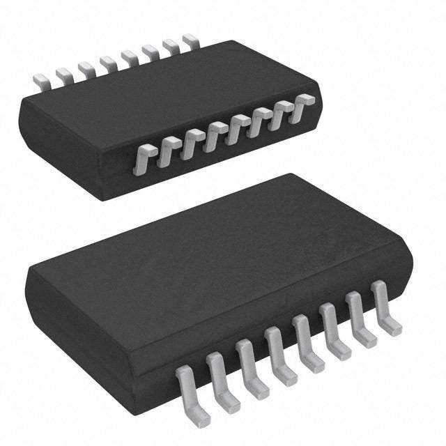
| 供应商器件封装 | 16-SOIC |
| 关闭 | No |
| 包装 | 管件 |
| 压摆率 | 2.4 V/µs |
| 双重电源电压 | +/- 5 V, +/- 9 V, +/- 12 V, +/- 15 V |
| 商标 | Analog Devices |
| 增益带宽生成 | 5 MHz |
| 增益带宽积 | 5MHz |
| 安装类型 | 表面贴装 |
| 安装风格 | SMD/SMT |
| 封装 | Tube |
| 封装/外壳 | 16-SOIC(0.295",7.50mm 宽) |
| 封装/箱体 | SOIC-16 |
| 工作温度 | -40°C ~ 85°C |
| 工作电源电压 | 9 V to 36 V |
| 工厂包装数量 | 47 |
| 放大器类型 | 通用 |
| 最大双重电源电压 | +/- 18 V |
| 最大工作温度 | + 85 C |
| 最小双重电源电压 | +/- 4.5 V |
| 最小工作温度 | - 40 C |
| 标准包装 | 47 |
| 电压-电源,单/双 (±) | ±4.5 V ~ 18 V |
| 电压-输入失调 | 50µV |
| 电压增益dB | 123.52 dB |
| 电流-电源 | 4mA |
| 电流-输入偏置 | 15nA |
| 电流-输出/通道 | - |
| 电源电压-最大 | 36 V |
| 电源电压-最小 | 9 V |
| 电源电流 | 4 mA |
| 电源类型 | Dual |
| 电路数 | 2 |
| 系列 | OP270 |
| 视频文件 | http://www.digikey.cn/classic/video.aspx?PlayerID=1364138032001&width=640&height=505&videoID=2245193153001http://www.digikey.cn/classic/video.aspx?PlayerID=1364138032001&width=640&height=505&videoID=2245193159001 |
| 转换速度 | 2.4 V/us |
| 输入补偿电压 | 50 uV |
| 输出类型 | - |
| 通道数量 | 2 Channel |


PDF Datasheet 数据手册内容提取
Dual Very Low Noise Precision Operational Amplifier Data Sheet OP270 FEATURES FUNCTIONAL BLOCK DIAGRAMS Very low noise density of 5 nV/√Hz at 1 kHz maximum –IN A 1 16 OUT A Excellent input offset voltage of 75 μV maximum +IN A 2 15 NC Low offset voltage drift of 1 μV/°C maximum NC 3 14 NC Very high gain of 1500 V/mV minimum V– 4 OP270 13 V+ Outstanding CMR of 106 dB minimum NC 5 12 NC +IN B 6 11 NC Slew rate of 2.4 V/μs typical –IN B 7 10 OUT B Gain bandwidth product of 5 MHz typical Industry-standard 8-lead dual pinout NC 8NC = NO CONNECT9 NC 00325-001 Figure 1. 16-Lead SOIC (S-Suffix) OUT A 1 8 V+ –IN A 2 A B 7 OUT B +INV A– 34 OP270 65 +–IINN BB 00325-002 Figure 2. 8-Lead PDIP (P-Suffix) 8-Lead CERDIP (Z-Suffix) GENERAL DESCRIPTION The OP270 is a high performance, monolithic, dual operational consumption of the dual OP270 is one-third less than two OP27 amplifier with exceptionally low voltage noise density (5 nV/√Hz devices, a significant advantage for power conscious applications. maximum at 1 kHz). It offers comparable performance to the The OP270 is unity-gain stable with a gain bandwidth product industry-standard OP27 from Analog Devices, Inc. of 5 MHz and a slew rate of 2.4 V/μs. The OP270 features an input offset voltage of less than 75 μV The OP270 offers excellent amplifier matching, which is and an offset drift of less than 1 μV/°C, guaranteed over the full important for applications such as multiple gain blocks, low military temperature range. Open-loop gain of the OP270 is more noise instrumentation amplifiers, dual buffers, and low noise than 1,500,000 into a 10 kΩ load, ensuring excellent gain accuracy active filters. and linearity, even in high gain applications. The input bias The OP270 conforms to the industry-standard 8-lead CERDIP current is less than 20 nA, which reduces errors due to signal and PDIP pinouts. source resistance. With a common-mode rejection (CMR) of For higher speed applications, the ADA4004-2 or the AD8676 greater than 106 dB and a power supply rejection ratio (PSRR) are recommended. For a quad op amp, see the OP470 data sheet. of less than 3.2 μV/V, the OP270 significantly reduces errors due to ground noise and power supply fluctuations. The power Rev. F Document Feedback Information furnished by Analog Devices is believed to be accurate and reliable. However, no responsibility is assumed by Analog Devices for its use, nor for any infringements of patents or other One Technology Way, P.O. Box 9106, Norwood, MA 02062-9106, U.S.A. rights of third parties that may result from its use. Specifications subject to change without notice. No license is granted by implication or otherwise under any patent or patent rights of Analog Devices. Tel: 781.329.4700 ©2001–2015 Analog Devices, Inc. All rights reserved. Trademarks and registered trademarks are the property of their respective owners. Technical Support www.analog.com
OP270 Data Sheet TABLE OF CONTENTS Features .............................................................................................. 1 Voltage and Current Noise ........................................................ 12 Functional Block Diagrams ............................................................. 1 Total Noise and Source Resistance ........................................... 12 General Description ......................................................................... 1 Noise Measurements .................................................................. 14 Revision History ............................................................................... 2 Capacitive Load Driving and Power Supply Considerations .... 15 Specifications ..................................................................................... 3 Unity-Gain Buffer Applications ............................................... 15 Electrical Specifications ............................................................... 4 Low Phase Error Amplifier ....................................................... 16 Absolute Maximum Ratings ............................................................ 5 Five-Band, Low Noise, Stereo Graphic Equalizer .................. 16 ESD Caution .................................................................................. 5 Digital Panning Control ............................................................ 17 Typical Performance Characteristics ............................................. 6 Dual Programmable Gain Amplifier ....................................... 17 Test Circuits ..................................................................................... 11 Outline Dimensions ....................................................................... 19 Applications Information .............................................................. 12 Ordering Guide .......................................................................... 20 REVISION HISTORY 10/15—Rev. E to Rev. F 4/03—Rev. B to Rev. C Changes to General Description Section ...................................... 1 Deletion of OP270A model ............................................... Universal Changes to Supply Voltage Parameter and Differential Input Edits to Features ................................................................................. 1 Voltage Parameter, Table 3 .............................................................. 5 Changes to Specifications ................................................................. 2 Deleted Table 4; Renumbered Sequentially .................................. 5 Deletion of Wafer Limits and Dice Characteristics ...................... 4 Changes to Absolute Maximum Ratings ........................................ 4 2/10—Rev. D to Rev. E Changes to Ordering Guide ............................................................. 4 Change to Input Noise Current Density Parameter, Table 1 ...... 3 Changes to Equations in Noise Measurements section ............. 10 Change to Figure 18 ......................................................................... 8 Change to Figure 10 ....................................................................... 11 Updated Outline Dimensions ....................................................... 14 2/09—Rev. C to Rev. D Updated Format .................................................................. Universal 11/02—Rev. A to Rev. B Reorganized Layout ............................................................ Universal Updated Ordering Guide .............................................................. 15 Changes to Figure 7 .......................................................................... 6 Changes to Figure 22 ........................................................................ 9 9/02—Rev. 0 to Rev. A Deleted Applications Heading ...................................................... 11 Edits to Absolute Maximum Ratings .............................................. 5 Changes to Figure 44 ...................................................................... 17 Edits to Ordering Guide ................................................................ 15 Changes to Figure 46 ...................................................................... 18 Updated Outline Dimensions ....................................................... 19 2/01—Revision 0: Initial Version Changes to Ordering Guide .......................................................... 20 Rev. F | Page 2 of 20
Data Sheet OP270 SPECIFICATIONS V = ±15 V, T = 25°C, unless otherwise noted. S A Table 1. OP270E OP270F OP270G Parameter Symbol Test Conditions Min Typ Max Min Typ Max Min Typ Max Unit Input Offset Voltage V 10 75 20 150 50 250 μV OS Input Offset Current I V = 0 V 1 10 3 15 5 20 nA OS CM Input Bias Current I V = 0 V 5 20 10 40 15 60 nA B CM Input Noise Voltage1 e p-p 0.1 Hz to 10 Hz 80 200 80 200 80 nV p-p n Input Noise Voltage Density2 e f = 10 Hz 3.6 6.5 3.6 6.5 3.6 nV/√Hz n O e f = 100 Hz 3.2 5.5 3.2 5.5 3.2 nV/√Hz n O e f = 1 kHz 3.2 5.0 3.2 5.0 3.2 nV/√Hz n O Input Noise Current Density i f = 10 Hz 1.1 1.1 1.1 pA/√Hz n O i f = 100 Hz 0.7 0.7 0.7 pA/√Hz n O i f = 1 kHz 0.6 0.6 0.6 pA/√Hz n O Large-Signal Voltage Gain A V = ±10 V, 1500 2300 1000 1700 750 1500 V/mV VO O R = 10 kΩ L V = ±10 V, 750 1200 500 900 350 700 V/mV O R = 2 kΩ L Input Voltage Range3 IVR ±12 ±12.5 ±12 ±12.5 ±12 ±12.5 V Output Voltage Swing V R ≥ 2 kΩ ±12 ±13.5 ±12 ±13.5 ±12 ±13.5 V O L Common-Mode Rejection CMR V = ±11 V 106 125 100 120 90 110 dB CM Power Supply Rejection PSRR V = ±4.5 V 0.56 3.2 1.0 5.6 1.5 5.6 μV/V S Ratio to ±18 V Slew Rate SR 1.7 2.4 1.7 2.4 1.7 2.4 V/μs Supply Current I No load 4 6.5 4 6.5 4 6.5 mA SY (All Amplifiers) Gain Bandwidth Product GBP 5 5 5 MHz Channel Separation1 CS V = ±20 V p-p, 125 175 125 175 175 dB O f = 10 Hz O Input Capacitance C 3 3 3 pF IN Input Resistance Differential Mode R 0.4 0.4 0.4 MΩ IN Common Mode R 20 20 20 GΩ INCM Settling Time t A = +1, 10 V, 5 5 5 μs S V step to 0.01% 1 Guaranteed but not 100% tested. 2 Sample tested. 3 Guaranteed by CMR test. Rev. F | Page 3 of 20
OP270 Data Sheet ELECTRICAL SPECIFICATIONS V = ±15 V, −40°C ≤ T ≤ 85°C, unless otherwise noted. S A Table 2. OP270E OP270F OP270G Parameter Symbol Test Conditions Min Typ Max Min Typ Max Min Typ Max Unit Input Offset Voltage V 25 150 45 275 100 400 μV OS Average Input Offset TCV 0.2 1 0.4 2 0.7 3 μV/°C OS Voltage Drift Input Offset Current I V = 0 V 1.5 30 5 40 15 50 nA OS CM Input Bias Voltage I V = 0 V 6 60 15 70 19 80 nA B CM Large-Signal Voltage Gain A V = ±10 V, 1000 1800 600 1400 400 1250 V/mV VO O R = 10 kΩ L A V = ±10 V, 500 900 300 700 225 670 V/mV VO O R = 2 kΩ L Input Voltage Range1 IVR ±12 ±12.5 ±12 ±12.5 ±12 ±12.5 V Output Voltage Swing V R ≥ 2 kΩ ±12 ±13.5 ±12 ±13.5 ±12 ±13.5 V O L Common-Mode Rejection CMR V = ±11 V 100 120 94 115 90 100 dB CM Power Supply Rejection PSRR V = ±4.5 V to ±18 V 0.7 5.6 1.8 10 2.0 1.5 μV/V S Ratio Supply Current I No load 4.4 7.2 4.4 7.2 4.4 7.2 mA SY (All Amplifiers) 1 Guaranteed by CMR test. Rev. F | Page 4 of 20
Data Sheet OP270 ABSOLUTE MAXIMUM RATINGS Table 3. Stresses at or above those listed under Absolute Maximum Parameter Rating Ratings may cause permanent damage to the product. This is a Supply Voltage ±18 V stress rating only; functional operation of the product at these Differential Input Voltage1 ±1.0 V or any other conditions above those indicated in the operational Differential Input Current1 ±25 mA section of this specification is not implied. Operation beyond Input Voltage Supply voltage the maximum operating conditions for extended periods may Output Short-Circuit Duration Continuous affect product reliability. Storage Temperature Range −65°C to +150°C ESD CAUTION Lead Temperature Range (Soldering, 60 sec) 300°C Junction Temperature (T) −65°C to +150°C J Operating Temperature Range −40°C to +85°C 1 The OP270 inputs are protected by back-to-back diodes. To achieve low noise performance, current-limiting resistors are not used. If the differential voltage exceeds +10 V, the input current should be limited to ±25 mA. Rev. F | Page 5 of 20
OP270 Data Sheet TYPICAL PERFORMANCE CHARACTERISTICS 10 10 9 TA = 25°C TA = 25°C 8 VS = ±15V VS = ±15V Hz) 7 Hz) √ 6 √ V/ A/ Y (n 5 Y (p T T SI 4 SI N N E E E D 3 E D 1 S S OI OI N 1/f CORNER = 5Hz N GE 2 NT TA RE 1/f CORNER = 200Hz L R O U V C 1 00352-004 0.1 00352-007 1 10 100 1k 10 100 1k 10k FREQUENCY (Hz) FREQUENCY (Hz) Figure 3. Voltage Noise Density vs. Frequency Figure 6. Current Noise Density vs. Frequency 5 40 TA = 25°C VS = ±15V Hz) 30 √ V/ 4 ENSITY (n AT 10kHz E (µV) 1200 E D 3 AT 1kHz AG OIS OLT 0 N V E TAG 2 –10 L O V 1 00352-005 ––3200 00352-008 0 ±5 ±10 ±15 ±20 –75 –50 –25 0 25 50 75 100 125 SUPPLY VOLTAGE (V) TEMPERATURE (°C) Figure 4. Voltage Noise Density vs. Supply Voltage Figure 7. Input Offset Voltage vs. Temperature 0.1Hz TO 10Hz NOISE 5 TA = 25°C VS = ±15V A) E (µ 4 G V) A V/DI OLT 3 n V 100 ET E ( FS G F A O 2 OLT E IN V G E N NOIS TTAS == ±2155°CV 00352-006 CHA 010 1 2 3 4 500352-009 TIME (1 sec/DIV) TIME (Minutes) Figure 5. 0.1 Hz to 10 Hz Input Voltage Noise Figure 8. Warm-Up Offset Voltage Drift Rev. F | Page 6 of 20
Data Sheet OP270 7 130 VS = ±15V TA = 25°C VCM = 0V 120 VS = ±15V 110 6 A) 100 n T ( 90 N CURRE 5 R (dB) 7800 S M BIA 4 C 60 T 50 U P N 40 I 3 30 2 00352-010 1200 00352-013 –75 –50 –25 0 25 50 75 100 125 1 10 100 1k 10k 100k 1M TEMPERATURE (°C) FREQUENCY (Hz) Figure 9. Input Bias Current vs. Temperature Figure 12. CMR vs. Frequency 5 6 VS = ±15V VCM = 0V nA) 4 mA) 5 T ( T ( N N E E RR 3 RR U U C C T Y 4 E L +125°C S P F 2 P OF SU +25°C UT AL –55°C P T 3 IN 1 TO 0 00352-011 2 00352-014 –75 –50 –25 0 25 50 75 100 125 0 ±5 ±10 ±15 ±20 TEMPERATURE (°C) SUPPLY VOLTAGE (V) Figure 10. Input Offset Current vs. Temperature Figure 13. Total Supply Current vs. Supply Voltage 7 8 TA = +25°C VS = ±15V VS = ±15V 7 6 A) RENT (nA) 5 RRENT (m 56 R U CU Y C 4 BIAS 4 UPPL 3 UT L S P A N T 2 I 3 TO 2 00352-012 01 00352-015 –10.0 –5.0 0 5.0 10.0 –75 –50 –25 0 25 50 75 100 125 –12.5 –7.5 –2.5 2.5 7.5 12.5 TEMPERATURE (°C) COMMON-MODE VOLTAGE (V) Figure 11. Input Bias Current vs. Common-Mode Voltage Figure 14. Total Supply Current vs. Temperature Rev. F | Page 7 of 20
OP270 Data Sheet 140 25 80 TA = 25°C TA = 25°C 120 20 VS = ±15V 100 s) e PHASE gre e PSR (dB)1068000 +PSR –PSR LOOP GAIN (dB) 11055 MARPGHAINS =E 62° 111642000 PHASE SHIFT (D EN- GAIN P 40 O 0 180 20 –5 01 10 100 F1kREQU1E0NkCY (H10z0)k 1M 10M 100M00352-016 –101 2 FREQUE3NCY (M4Hz) 5 6 7 8 9 10 00352-019 Figure 15. PSR vs. Frequency Figure 18. Open-Loop Gain and Phase Shift vs. Frequency 140 5000 TA = 25°C VS = ±15V 120 4000 B) 100 mA) GAIN (d 80 AIN (V/ 3000 OP P G EN-LO 60 N-LOO 2000 P E O 40 P O 1000 20 0 00352-017 0 00352-020 1 10 100 1k 10k 100k 1M 10M 100M 0 ±5 ±10 ±15 ±20 ±25 FREQUENCY (Hz) SUPPLY VOLTAGE (V) Figure 16. Open-Loop Gain vs. Frequency Figure 19. Open-Loop Gain vs. Supply Voltage 80 80 TA = 25°C VS = ±15V 8 Hz) 60 M B) s) 70 T ( N (d gree 7 DUC CLOSED-LOOP GAI 2400 PHASE MARGIN (De 5600 Ф GBP 56 N BANDWIDTH PRO 0 AI G –201k 10k FREQU1E0N0kCY (Hz) 1M 10M00352-018 40–75 –50 –25 0TEMP2E5RATU5R0E (°C7)5 100 125 1504 00352-021 Figure 17. Closed-Loop Gain vs. Frequency Figure 20. Phase Margin and Gain Bandwidth Product vs. Temperature Rev. F | Page 8 of 20
Data Sheet OP270 28 100 TA = 25°C TA = 25°C VS = ±15V VS = ±15V 24 THD = 1% V) AV = 1 G ( 20 Ω) 75 WIN CE ( S N UT 16 DA TP PE 50 U M M O 12 UT I AV = 10 MU TP AV = 100 AXI 8 OU 25 M 4 0 00352-022 0 00352-025 1k 10k 100k 1M 10M 1k 10k 100k 1M 10M FREQUENCY (Hz) FREQUENCY (Hz) Figure 21. Maximum Output Swing vs. Frequency Figure 24. Output Impedance vs. Frequency 15 2.8 TA = 25°C VS = ±15V 14 VS = ±15V POSITIVE SWING E (V) 13 2.7 G A 12 T VOLT 11 NSWEGINAGTIVE E (V/µs) 2.6 PU 10 AT 2.5 T R OU 9 W –SR MUM 8 SLE 2.4 XI +SR MA 7 2.3 56 00352-023 2.2 00352-026 100 1k 10k –75 –50 –25 0 25 50 75 100 125 LOAD RESISTANCE (Ω) TEMPERATURE (°C) Figure 22. Maximum Output Voltage vs. Load Resistance Figure 25. Slew Rate vs. Temperature 50 190 TA = 25°C VS = ±15V 180 HOOT (%) 40 VAIVN == +1100mV ON (dB) 111567000 SIGNAL OVERS 2300 NEL SEPARATI 111123410000 ALL- HAN 100 M 10 C S 90 TA = 25°C 0 00352-024 7800 VVSO == ±2105VV p-p TO 10kHz 00352-027 0 200 400 600 800 1000 1 10 100 1k 10k 100k 1M CAPACITIVE LOAD (pF) FREQUENCY (Hz) Figure 23. Small-Signal Overshoot vs. Capacitive Load Figure 26. Channel Separation vs. Frequency Rev. F | Page 9 of 20
OP270 Data Sheet 0.1 TA = 25°C TA = 25°C VS = ±15V VS = ±15V %) VO = 20V p-p AV = +1 N ( RL = 2kΩ RL = 2kΩ O RTI AV = 10 O T S DI C 0.01 NI O M R A H L AV = 1 A T O T 0.001 00352-028 50mV 200ns 00352-030 10 100 1k 10k FREQUENCY (Hz) Figure 27. Total Harmonic Distortion vs. Frequency Figure 29. Small-Signal Transient Response TA = 25°C VS = ±15V AV = +1 RL = 2kΩ 5V 20µs 00352-029 Figure 28. Large-Signal Transient Response Rev. F | Page 10 of 20
Data Sheet OP270 TEST CIRCUITS 5kΩ 500Ω 1/2 OP270 V1 20Vp-p 5kΩ 50Ω 1/2 OP270 V2 CHANNEL SEPARATION = 20 LOG V2V/11000 00325-031 Figure 30. Channel Separation Test Circuit +18V 8 100kΩ 2 1/2 1 OP270 3 200kΩ 6 1/2 7 OP270 100kΩ 5 4 –18V 00325-032 Figure 31. Burn-In Circuit Rev. F | Page 11 of 20
OP270 Data Sheet APPLICATIONS INFORMATION VOLTAGE AND CURRENT NOISE Figure 33 also shows the relationship between total noise and source resistance, but at 10 Hz. Total noise increases more The OP270 is a very low noise dual op amp, exhibiting a typical quickly than shown in Figure 32 because current noise is voltage noise density of only 3.2 nV/√Hz at 1 kHz. Because the inversely proportional to the square root of frequency. In voltage noise is inversely proportional to the square root of the Figure 33, the current noise of the OP270 dominates the total collector current, the exceptionally low noise characteristic of noise when R is greater than 5 kΩ. the OP270 is achieved in part by operating the input transistors S at high collector currents. Current noise, however, is directly Figure 32 and Figure 33 show that to reduce total noise, source proportional to the square root of the collector current. As a resistance must be kept to a minimum. In applications with a result, the outstanding voltage noise density performance of the high source resistance, the OP200, with lower current noise OP270 is gained at the expense of current noise performance, than the OP270, can provide lower total noise. which is normal for low noise amplifiers. 100 To obtain the best noise performance in a circuit, it is vital to understand the relationships among voltage noise (e), current n noise (in), and resistor noise (et). Hz) √ TOTAL NOISE AND SOURCE RESISTANCE V/ n E ( OP200 The total noise of an op amp can be calculated by S 10 OI N En (en)2 (inRs)2 (et)2 OTAL OP270 T where: Eenn iiss tthhee otopt aaml inpp vuotl-traegfee rnroeids en. oise. 1 RNEOSISISET OONRLY 00352-034 in is the op amp current noise. 100 1k 10k 100k e is the source resistance thermal noise. SOURCE RESISTANCE (Ω) t R is the source resistance. Figure 33. Total Noise vs. Source Resistance S (Including Resistor Noise) at 10 Hz The total noise is referred to the input and at the output is Figure 34 shows peak-to-peak noise vs. source resistance over amplified by the circuit gain. the 0.1 Hz to 10 Hz range. At low values of R, the voltage noise S Figure 32 shows the relationship between total noise at 1 kHz of the OP270 is the major contributor to peak-to-peak noise, and source resistance. When RS is less than 1 kΩ, the total noise with current noise becoming the major contributor as RS is dominated by the voltage noise of the OP270. As RS rises increases. The crossover point between the OP270 and the above 1 kΩ, total noise increases and is dominated by resistor OP200 for peak-to-peak noise is at a source resistance of 17 kΩ. noise rather than by the voltage or current noise of the OP270. 1k When R exceeds 20 kΩ, the current noise of the OP270 S becomes the major contributor to total noise. OP200 100 V) n E ( S OI N V/√Hz) O-PEAK 100 NOISE (n 10 OP200 PEAK-T OP270RESISTOR L NOISE ONLY TOTA OP270 10 00352-035 100 1k 10k 100k 1 RNEOSISISET OONRLY 00352-033 Figure 34. Peak-to-Pe(aInk cNSluOodiUsiRen Cg(0E R. 1Re sHEiSsztI StooTr A1NN0o CHisEze )() Ω v)s. Source Resistance 100 1k 10k 100k SOURCE RESISTANCE (Ω) Figure 32. Total Noise vs. Source Resistance (Including Resistor Noise) at 1 kHz Rev. F | Page 12 of 20
Data Sheet OP270 For reference, typical source resistances of some signal sources are listed in Table 4. Table 4. Typical Source Resistances Device Source Impedance Comments Strain Gage <500 Ω Typically used in low frequency applications. Magnetic Tapehead, Microphone <1500 Ω Low I is very important to reduce self-magnetization problems when B direct coupling is used. OP270 I can be disregarded. B Magnetic Phonograph Cartridge <1500 Ω Low I is important to reduce self-magnetization problems in direct-coupled B applications. OP270 does not introduce any self-magnetization problems. Linear Variable Differential Transformer <1500 Ω Used in rugged servo-feedback applications. The bandwidth of interest is 400 Hz to 5 kHz. R3 1.24kΩ R1 5Ω R2 OP270 C1 C4 5Ω DUT 2µF 0.22µF OP27E D1, D2 1N4148 90R95Ω 600RΩ6 OP27E 65R.41k0Ω 65R.41k1Ω R14 4.99kΩ 200RΩ4 30R69Ω 0.22CµF3 OP42E C5 eOUT R13 1µF 5.9kΩ R8 10kΩ 0.0C322µF 10Rk1Ω2 GVSA I=N ± =1 55V0,000 00325-036 Figure 35. Peak-to-Peak Voltage Noise Test Circuit (0.1 Hz to 10 Hz) Rev. F | Page 13 of 20
OP270 Data Sheet NOISE MEASUREMENTS Noise Measurement—Noise Voltage Density Peak-to-Peak Voltage Noise The circuit of Figure 37 shows a quick and reliable method for measuring the noise voltage density of dual op amps. The first The circuit of Figure 35 is a test setup for measuring peak-to- amplifier is in unity gain, with the final amplifier in a noninverting peak voltage noise. To measure the 200 nV peak-to-peak noise gain of 101. Because the noise voltages of the amplifiers are specification of the OP270 in the 0.1 Hz to 10 Hz range, the uncorrelated, they add in rms to yield following precautions must be observed: The device has to be warmed up for at least five minutes. e 101 e 2 e 2 OUT nA nB As shown in the warm-up drift curve (see Figure 8), the The OP270 is a monolithic device with two identical amplifiers. offset voltage typically changes 2 μV due to increasing chip Therefore, the noise voltage densities of the amplifiers match, temperature after power-up. In the 10 sec measurement giving interval, these temperature-induced effects can exceed tens of nanovolts. e 101 2e 2101 2e OUT n n For similar reasons, the device has to be well shielded from R1 R2 air currents. Shielding also minimizes thermocouple effects. 100Ω 10kΩ Sudden motion in the vicinity of the device can also feed through to increase the observed noise. 1/2 The test time to measure noise of 0.1 Hz to 10 Hz should OP270 eOUT 1/2 not exceed 10 sec. As shown in the noise-tester frequency OP270 TO SPECTRUM ANALYZER roenslpyo onnsee pcuorlev.e T ohfe F tiegsutr tei m36e, othf e1 00 .s1e cH azc ctso rans earn i sa dddefitinioenda bl y VeOS U=T ±(1n5VV/√Hz) ≈ 101 (√2en) 00325-038 pole to eliminate noise contribution from the frequency Figure 37. Noise Voltage Density Test Circuit band below 0.1 Hz. Noise Measurement—Current Noise Density A noise voltage density test is recommended when measuring The test circuit shown in Figure 38 can be used to measure current noise on several units. A 10 Hz noise voltage density mea- noise density. The formula relating the voltage output to the current surement correlates well with a 0.1 Hz to 10 Hz peak-to-peak noise density is noise reading because both results are determined by the white noise and the location of the 1/f corner frequency. enOUT 2 40nV/ Hz2 Power should be supplied to the test circuit by well bypassed G i low noise supplies, such as batteries. Such supplies will min- n R S imize output noise introduced via the amplifier supply pins. where: 100 G is a gain of 10,000. R = 100 kΩ source resistance. S 80 R3 1.24kΩ B) 60 5RΩ1 10R02kΩ d N ( OP270 GAI 40 DUT OP27E enOUT TO SPECTRUM ANALYZER R5 8.06kΩ 20 0 00352-037 200RΩ4 GVSA I=N ± =1 51V0,000 00325-039 0.01 0.1 1 10 100 Figure 38. Current Noise Density Test Circuit FREQUENCY (Hz) Figure 36. 0.1 Hz to 10 Hz Peak-to-Peak Voltage Noise Test Circuit Frequency Response Rev. F | Page 14 of 20
Data Sheet OP270 CAPACITIVE LOAD DRIVING AND POWER SUPPLY UNITY-GAIN BUFFER APPLICATIONS CONSIDERATIONS When R ≤ 100 Ω and the input is driven with a fast, large signal f The OP270 is unity-gain stable and capable of driving large pulse (>1 V), the output waveform looks like the one in Figure 40. capacitive loads without oscillating. Nonetheless, good supply During the fast feedthrough-like portion of the output, the input bypassing is highly recommended. Proper supply bypassing protection diodes effectively short the output to the input, and reduces problems caused by supply line noise and improves the a current, limited only by the output short-circuit protection, is capacitive load driving capability of the OP270. drawn by the signal generator. With R ≥ 500 Ω, the output is f In the standard feedback amplifier, the output resistance of the capable of handling the current requirements (IL ≤ 20 mA at 10 V); op amp combines with the load capacitance to form a low-pass the amplifier stays in its active mode and a smooth transition occurs. filter that adds phase shift in the feedback network and reduces When R > 3 kΩ, a pole created by R and the input capacitance f f stability. A simple circuit to eliminate this effect is shown in (3 pF) of the amplifier creates additional phase shift and reduces Figure 39. The components C1 and R3 decouple the amplifier phase margin. A small capacitor (20 pF to 50 pF) in parallel with from the load capacitance and provide additional stability. The R helps eliminate this problem. f values of C1 and R3 shown in Figure 39 are for a load capacitance Rf of up to 1000 pF when used with the OP270. V+ +C2 C3 10µF OP270 2.4V/µs 0.1µF VIN R1 200CpF1 RR23 Figure 40. Pulsed Operation 00325-041 50Ω OP270 VOUT C1 1000pF C5 C4 0.1µF +10µF V– PCLAAPCAEC ISTUOPRP ALTY ODPE2C7O0UPLING 00325-040 Figure 39. Driving Large Capacitive Loads Rev. F | Page 15 of 20
OP270 Data Sheet LOW PHASE ERROR AMPLIFIER 0 The simple amplifier depicted in Figure 41 utilizes a monolithic –1 SINGLE OP AMP. dual operational amplifier and a few resistors to substantially CONVENTIONAL DESIGN reduce phase error compared with conventional amplifier es) –2 e designs. At a given gain, the frequency range for a specified gr e D –3 phase accuracy is more than a decade greater than that of a T ( CASCADED standard single op amp amplifier. HIF (TWO STAGES) S –4 E The low phase error amplifier performs second-order fre- AS quency compensation through the response of Op Amp A2 in PH –5 LOW PHASE ERROR AMPLIFIER the feedback loop of A1. Both op amps must be extremely well –6 mfeeadtcbhaecdk ilno ofrpe fqourecnesc yV re/(sKpo1n +s e1. )A =t Vlow. fTrehqeu Aen2 cfieeesd, bthaec kA l1o op –7 00352-043 2 IN 0.001 0.01 0.1 1 forces V /(K1 + 1) = V/(K1 + 1), yielding an overall transfer 0.005 0.05 0.5 O 2 FREQUENCY RATIO (1/βω)(ω/ωT) function of V /V = K1 + 1. The dc gain is determined by the O IN Figure 42. Phase Error Comparison resistor divider at the output, V , and is not directly affected by O the resistor divider around A2. Note that, like a conventional FIVE-BAND, LOW NOISE, STEREO GRAPHIC single op amp amplifier, the dc gain is set by resistor ratios only. EQUALIZER Minimum gain for the low phase error amplifier is 10. The graphic equalizer circuit shown in Figure 43 provides 15 dB R2 R2 = R1 of boost or cut over a five-band range. Signal-to-noise ratio over R2 a 20 kHz bandwidth is better than 100 dB and referred to a 3 V K2 rms input. Larger inductors can be replaced by active inductors, 1/2 but consequently reduces the signal-to-noise ratio. OPA2270E V2 C1 0.47µF VIN 1/2 3.R3k2Ω R1 OP270E R14 47kΩ 1/2 100Ω OP270E VOUT R1 1/2 R1 K1 R4 OP270E 1kΩ VIN A1 68R03Ω 6+.C82µF L1 60Hz 3R.31k3Ω VO TANTALUM 1H R6 ASSUME A1 AAON(Ds )A =2 ωAsTRE MATCHED. VO = (K1 + 1)VIN 00325-042 68R05Ω +1Cµ3F L2 1kΩ200Hz Figure 41. Low Phase Error Amplifier TANTALUM 600mH R8 Fpihgausree e 4r2ro cro ammppalriefise trh we ipthh aas ceo enrvroenr tpioenrfaolr sminagnlcee o opf atmhep l ow 68R07Ω 0+.2C24µF L3 1kΩ800Hz 180mH amplifier and a cascaded two-stage amplifier. The low phase R10 efrrerqour eanmcpielsif wiehr esrheo ωw/sβ aω mT <u c0h.1 l.o Fwoerr epxhaamsep leer,r ao rp, hpaasret iecrurloarr loyf for 68R09Ω 0.+0C475µF L4 1kΩ3kHz 60mH −0.1° occurs at 0.002 ω/βω for the single op amp amplifier, but T R12 a t 0.11 ω/βωT for the low phase error amplifier. 6R8101Ω 0.+0C226µF 10Lm5H 1kΩ10kHz 00325-044 Figure 43. Five-Band, Low Noise Graphic Equalizer Rev. F | Page 16 of 20
Data Sheet OP270 DIGITAL PANNING CONTROL +5V +15V Figure 44 uses a DAC8221 (a dual 12-bit CMOS DAC) to pan a 21 VDD signal between two channels. One channel is formed by the DAC8221P 0.01µF current output of DAC A driving one-half of an OP270 in a RFBA 3 current-to-voltage converter configuration. The other channel + is formed by the complementary output current of DAC A, 10µF – wcohmicphl enmoremntaalrlyy cfluorwresn tto igs rcoounnvde rttherdo tuog ah vthoelt aAgGe NbyD t hpein o. tThehri s VIN 4 VREFA DAC A IOUTA 2 2 1/28 1 OP270GP OUT half of the OP270, which also holds AGND at virtual ground. AGND 1 3 4 DAC DATA BUS Gain error due to mismatching between the internal DAC PINS 6(MSB) TO 17 (LSB) + 0.1µF 10µF ladder resistors and the current-to-voltage feedback resistors is – RFBB 23 –15V eliminated by using feedback resistors internal to the DAC8221. Only DAC A passes a signal; DAC B provides the second NC 22 VREFB DAC B IOUTB 24 6 feedback resistor. With VREFB unconnected, the current-to- OP217/20GP 7 OUT voltage converter, using R , is accurate and not influenced by 18 5 FBB DAC A/DAC B digital data reaching DAC B. Distortion of the digital panning control is less than 0.002% over the 20 Hz to 20 kHz audio 19 WRITE CS range. Figure 45 shows the complementary outputs for a 1 kHz CONTROL 20 WR iDnpUuAt Lsi gPnRalO anGdR aA dMigMitaAl rBamLEp aGpAplIiNed AtoM thPeL DIFAICE Rda ta input. DGN5D 00325-045 Figure 44. Digital Panning Control The dual OP270 and the DAC8221 (a dual 12-bit CMOS DAC) can be combined to form a space-saving, dual programmable amplifier. The digital code present at the DAC, which is easily set by a microprocessor, determines the ratio between the internal A OUT feedback resistor and the resistance that the DAC ladder presents to the op amp feedback loop. Gain of each amplifier is V 4096 O V n IN where n is the decimal equivalent of the 12-bit digital code A OUT present at the DAC. If the digital code present at the DAC consists of all 0s, the 5V 5V 1ms 00352-046 feedback loop opens, causing the op amp output to saturate. A Figure 45. Digital Panning Control Output 20 MΩ resistor placed in parallel with the DAC feedback loop eliminates this problem with only a very small reduction in gain accuracy. Rev. F | Page 17 of 20
OP270 Data Sheet +15V +5V 21 0.01µF DAC8221P VDD VREFA 4 VINA 3 RFBA 20MΩ +10µF – DAC A IOUTA 2 2 8 1/2 1 OP270EZ 3 VOUTA 4 AGND 1 + 0.1µF 10µF 23 RFBB –15V – VINB IOUTB 24 6 DAC B 1/2 7 OP270GP 20MΩ 5 VOUTB DAC DATA BUS PINS 6 (MSB) TO 17 (LSB) 18 VREFB 22 WRITE 19 CONTROL 20 DGN5D 00325-047 Figure 46. Dual Programmable Gain Amplifier V+ BIAS OUT –IN +IN V– 00325-003 Figure 47. Simplified Schematic (One of Two Amplifiers Is Shown) Rev. F | Page 18 of 20
Data Sheet OP270 OUTLINE DIMENSIONS 0.005 (0.13) 0.055 (1.40) MIN MAX 8 5 0.310 (7.87) 0.220 (5.59) 1 4 0.100 (2.54) BSC 0.405 (10.29) MAX 0.320 (8.13) 0.290 (7.37) 0.200 (5.08) 0.060 (1.52) MAX 0.015 (0.38) 0.200 (5.08) 0.150 (3.81) MIN 0.125 (3.18) 0.015 (0.38) 00..002134 ((00..5386)) 0.070 (1.78) SPELAANTIENG 1 05°° 0.008 (0.20) 0.030 (0.76) CONTROLLING DIMENSIONS ARE IN INCHES; MILLIMETER DIMENSIONS (IN PARENTHESES) ARE ROUNDED-OFF INCH EQUIVALENTS FOR REFERENCE ONLY AND ARE NOT APPROPRIATE FOR USE IN DESIGN. Figure 48. 8-Lead Ceramic Dual In-Line Package [CERDIP] Z-Suffix (Q-8) Dimensions shown in inches and (millimeters) 0.400 (10.16) 0.365 (9.27) 0.355 (9.02) 8 5 0.280 (7.11) 0.250 (6.35) 1 4 0.240 (6.10) 0.325 (8.26) 0.310 (7.87) 0.100 (2.54) 0.300 (7.62) BSC 0.060 (1.52) 0.195 (4.95) 0.210 (5.33) MAX 0.130 (3.30) MAX 0.115 (2.92) 0.015 0.150 (3.81) (0.38) 0.015 (0.38) 0.130 (3.30) MIN GAUGE 0.115 (2.92) SEATING PLANE 0.014 (0.36) PLANE 0.010 (0.25) 0.022 (0.56) 0.008 (0.20) 0.005 (0.13) 0.430 (10.92) 0.018 (0.46) MIN MAX 0.014 (0.36) 0.070 (1.78) 0.060 (1.52) 0.045 (1.14) COMPLIANTTO JEDEC STANDARDS MS-001 CONTROLLING DIMENSIONSARE IN INCHES; MILLIMETER DIMENSIONS (RCINEOFRPENAREREREN NLCTEEHA EODSNSEL MSY)AAAYNR BDEE AR CROOEU NNNFODIGETUDAR-POEPFDRFOA INSPC RWHIAH ETOEQL UFEIO VORAR LU EHSNAETL ISFN FLDOEEARSDIGSN.. 070606-A Figure 49. 8-Lead Plastic Dual In-Line Package [PDIP] Narrow Body P-Suffix (N-8) Dimensions shown in inches and (millimeters) Rev. F | Page 19 of 20
OP270 Data Sheet 10.50 (0.4134) 10.10 (0.3976) 16 9 7.60 (0.2992) 7.40 (0.2913) 1 10.65 (0.4193) 8 10.00 (0.3937) 1.27 (0.0500) 0.75 (0.0295) BSC 2.65 (0.1043) 0.25 (0.0098) 45° 0.30 (0.0118) 2.35 (0.0925) 8° 0.10 (0.0039) 0° COPLANARITY 0.10 0.51 (0.0201) SPELAATNIENG 0.33 (0.0130) 1.27 (0.0500) 0.31 (0.0122) 0.20 (0.0079) 0.40 (0.0157) COMPLIANTTO JEDEC STANDARDS MS-013-AA C(RINOEFNPETARRREOENNLCLTEIHN EOGSN EDLSIYM)AEANNRDSEI AORRNOESU NANORDEET DAIN-PO MPFRIFLO LMPIIMRLELIATIMTEEER TFSEO; RIRN ECUQHSU EDI VIINMA LEDENENSSTIIOGSN NFS.OR 032707-B Figure 50. 16-Lead Standard Small Outline Package [SOIC_W] Wide Body S-Suffix (RW-16) Dimensions shown in millimeters and (inches) ORDERING GUIDE T = +25°C θ θ 2 Package A JC JA Model1 V Max (μV) (°C/W) (°C/W) Temperature Range Package Description Option OS OP270EZ 75 12 134 −40°C to +85°C 8-Lead CERDIP Q-8 (Z-Suffix) OP270FZ 150 12 134 −40°C to +85°C 8-Lead CERDIP Q-8 (Z-Suffix) OP270GP 250 37 96 −40°C to +85°C 8-Lead PDIP N-8 (P-Suffix) OP270GPZ −40°C to +85°C 8-Lead PDIP N-8 (P-Suffix) OP270GS 250 27 92 −40°C to +85°C 16-Lead SOIC_W RW-16 (S-Suffix) OP270GS-REEL −40°C to +85°C 16-Lead SOIC_W RW-16 (S-Suffix) OP270GSZ −40°C to +85°C 16-Lead SOIC_W RW-16 (S-Suffix) OP270GSZ-REEL −40°C to +85°C 16-Lead SOIC_W RW-16 (S-Suffix) 1 The OP270GPZ, OP270GSZ, and OP270GSZ-REEL are RoHS compliant parts. 2 θJA is specified for worst-case mounting conditions, that is, θJA is specified for device in socket for CERDIP and PDIP packages; θJA is specified for device soldered to printed circuit board for SOIC package. ©2001–2015 Analog Devices, Inc. All rights reserved. Trademarks and registered trademarks are the property of their respective owners. D00325-0-10/15(F) Rev. F | Page 20 of 20