ICGOO在线商城 > 射频/IF 和 RFID > RF 评估和开发套件,板 > OM7623/BFU725F/1500,598

 Datasheet下载
- 型号: OM7623/BFU725F/1500,598
- 制造商: NXP Semiconductors
- 库位|库存: xxxx|xxxx
- 要求:
| 数量阶梯 | 香港交货 | 国内含税 |
| +xxxx | $xxxx | ¥xxxx |
查看当月历史价格
查看今年历史价格
OM7623/BFU725F/1500,598产品简介:
ICGOO电子元器件商城为您提供OM7623/BFU725F/1500,598由NXP Semiconductors设计生产,在icgoo商城现货销售,并且可以通过原厂、代理商等渠道进行代购。 OM7623/BFU725F/1500,598价格参考。NXP SemiconductorsOM7623/BFU725F/1500,598封装/规格:RF 评估和开发套件,板, 。您可以下载OM7623/BFU725F/1500,598参考资料、Datasheet数据手册功能说明书,资料中有OM7623/BFU725F/1500,598 详细功能的应用电路图电压和使用方法及教程。
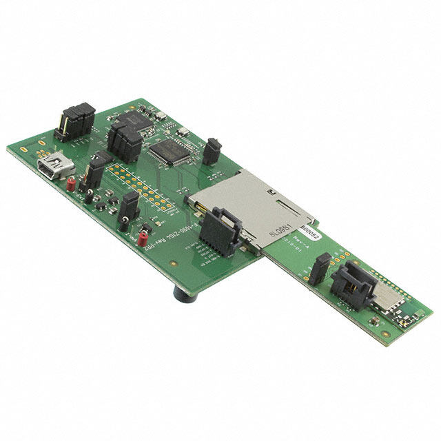
型号为OM7623/BFU725F/1500,598、品牌为NXP USA Inc.的RF评估和开发套件,主要用于射频(RF)电路的设计、测试与性能验证。该开发套件集成了NXP高性能的BFU725F低噪声放大器(LNA)等关键射频元件,适用于工作频率在1.5 GHz左右的无线通信系统开发。

其典型应用场景包括无线基础设施(如小基站、分布式天线系统)、工业物联网(IIoT)、智能城市无线节点、短距离高频通信设备以及车载通信模块的研发与调试。该套件帮助工程师快速评估BFU725F器件在实际环境中的增益、噪声系数、线性度和功耗等关键参数,加速产品原型设计和优化。

此外,该评估板支持灵活配置,便于进行阻抗匹配测试、滤波器集成验证及多频段系统兼容性分析,广泛适用于研发实验室、高校科研项目以及射频模块制造商的技术验证阶段。通过简化射频设计流程,提升开发效率,缩短产品上市周期。
| 参数 | 数值 |
| 产品目录 | |
| 描述 | EVAL BOARD FOR BFU725F 1.5GHZ |
| 产品分类 | |
| 品牌 | NXP Semiconductors |
| 数据手册 | |
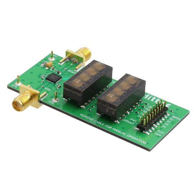
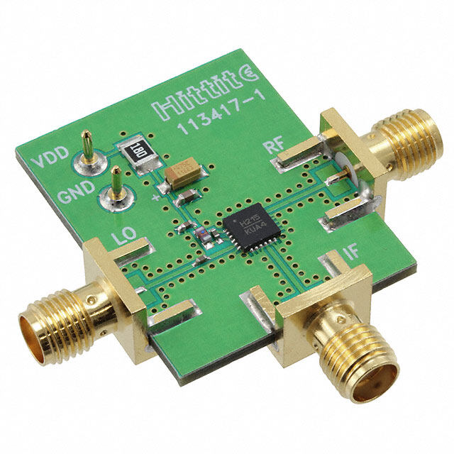
| 产品图片 |
|
| 产品型号 | OM7623/BFU725F/1500,598 |
| rohs | 无铅 / 库存产品核实请求 |
| 产品系列 | - |
| 产品培训模块 | http://www.digikey.cn/PTM/IndividualPTM.page?site=cn&lang=zhs&ptm=25714 |
| 其它名称 | 568-8515 |
| 所含物品 | 板 |
| 标准包装 | 1 |
| 类型 | |
| 配套使用产品/相关产品 | BFU725F |
| 频率 | 1.5GHz |


- 商务部:美国ITC正式对集成电路等产品启动337调查
- 曝三星4nm工艺存在良率问题 高通将骁龙8 Gen1或转产台积电
- 太阳诱电将投资9.5亿元在常州建新厂生产MLCC 预计2023年完工
- 英特尔发布欧洲新工厂建设计划 深化IDM 2.0 战略
- 台积电先进制程称霸业界 有大客户加持明年业绩稳了
- 达到5530亿美元!SIA预计今年全球半导体销售额将创下新高
- 英特尔拟将自动驾驶子公司Mobileye上市 估值或超500亿美元
- 三星加码芯片和SET,合并消费电子和移动部门,撤换高东真等 CEO
- 三星电子宣布重大人事变动 还合并消费电子和移动部门
- 海关总署:前11个月进口集成电路产品价值2.52万亿元 增长14.8%

PDF Datasheet 数据手册内容提取
BFU725F/N1 NPN wideband silicon germanium RF transistor Rev. 2 — 3 November 2011 Product data sheet 1. Product profile 1.1 General description NPN silicon germanium microwave transistor for high speed, low noise applications in a plastic, 4-pin dual-emitter SOT343F package. CAUTION This device is sensitive to ElectroStatic Discharge (ESD). Observe precautions for handling electrostatic sensitive devices. Such precautions are described in the ANSI/ESD S20.20, IEC/ST61340-5, JESD625-A or equivalent standards. 1.2 Features and benefits Low noise high gain microwave transistor Noise figure (NF)=0.7dB at 5.8GHz High maximum stable gain 27dB at 1.8GHz 110GHz f silicon germanium technology T 1.3 Applications 2nd LNA stage and mixer stage in DBS LNB’s Satellite radio Low noise amplifiers for microwave communications systems WLAN and CDMA applications Analog/digital cordless applications Ka band oscillators (DRO’s) 1.4 Quick reference data Table 1. Quick reference data Symbol Parameter Conditions Min Typ Max Unit V collector-base voltage open emitter - - 10 V CBO V collector-emitter voltage open base - - 2.8 V CEO V emitter-base voltage open collector - - 1.0 V EBO I collector current - 25 40 mA C P total power dissipation T 90C [1] - - 136 mW tot sp h DC current gain I =10mA; V =2V; 160 280 400 FE C CE T =25C j
BFU725F/N1 NXP Semiconductors NPN wideband silicon germanium RF transistor Table 1. Quick reference data …continued Symbol Parameter Conditions Min Typ Max Unit C collector-base V =2V; f=1MHz - 70 - fF CBS CB capacitance f transition frequency I =25mA; V =2V; - 55 - GHz T C CE f=2GHz; T =25C amb G maximum power gain I =25mA; V =2V; [2] - 18 - dB p(max) C CE f=5.8GHz; T =25C amb NF noise figure I =5mA; V =2V; - 0.7 - dB C CE f=5.8GHz; = ; S opt T =25C amb [1] T is the temperature at the solder point of the emitter lead. sp [2] G is the maximum power gain, if K>1. If K<1 then G =Maximum Stable Gain (MSG). p(max) p(max) 2. Pinning information Table 2. Discrete pinning Pin Description Simplified outline Graphic symbol 1 emitter 3 4 4 2 base 3 emitter 2 4 collector 1, 3 2 1 mbb159 3. Ordering information Table 3. Ordering information Type number Package Name Description Version BFU725F/N1 - plastic surface-mounted flat pack package; reverse SOT343F pinning; 4 leads 4. Marking Table 4. Marking Type number Marking Description BFU725F/N1 B7* * = p : made in Hong Kong * = t : made in Malaysia * = W : made in China BFU725F_N1 All information provided in this document is subject to legal disclaimers. © NXP B.V. 2011. All rights reserved. Product data sheet Rev. 2 — 3 November 2011 2 of 12
BFU725F/N1 NXP Semiconductors NPN wideband silicon germanium RF transistor 5. Limiting values Table 5. Limiting values In accordance with the Absolute Maximum Rating System (IEC 60134). Symbol Parameter Conditions Min Max Unit V collector-base voltage open emitter - 10 V CBO V collector-emitter voltage open base - 2.8 V CEO V emitter-base voltage open collector - 1.0 V EBO I collector current - 40 mA C P total power dissipation T 90C [1] - 136 mW tot sp T storage temperature 65 +150 C stg T junction temperature - 150 C j [1] T is the temperature at the solder point of the emitter lead. sp 6. Thermal characteristics Table 6. Thermal characteristics Symbol Parameter Conditions Typ Unit R thermal resistance from junction to solder point 440 K/W th(j-sp) 001aah424 200 Ptot (mW) 150 100 50 0 0 40 80 120 160 Tsp (°C) Fig 1. Power derating curve BFU725F_N1 All information provided in this document is subject to legal disclaimers. © NXP B.V. 2011. All rights reserved. Product data sheet Rev. 2 — 3 November 2011 3 of 12
BFU725F/N1 NXP Semiconductors NPN wideband silicon germanium RF transistor 7. Characteristics Table 7. Characterist ics T =25C unless otherwise specified. j Symbol Parameter Conditions Min Typ Max Unit V collector-base breakdown I =2.5A; I =0mA 10 - - V (BR)CBO C E voltage V collector-emitter breakdown I =1mA; I =0mA 2.8 - - V (BR)CEO C B voltage I collector current - 25 40 mA C I collector-base cut-off current I =0mA; V =4.5V - - 100 nA CBO E CB h DC current gain I =10mA; V =2V 160 280 400 FE C CE C collector-emitter capacitance V =2V; f=1MHz - 268 - fF CES CB C emitter-base capacitance V =0.5V; f=1MHz - 400 - fF EBS EB C collector-base capacitance V =2V; f=1MHz - 70 - fF CBS CB f transition frequency I =25mA; V =2V; f=2GHz; T =25C - 55 - GHz T C CE amb G maximum power gain I =25mA; V =2V; T =25C [1] p(max) C CE amb f=1.5GHz - 28 - dB f=1.8GHz - 27 - dB f=2.4GHz - 25.5 - dB f=5.8GHz - 18 - dB f=12GHz - 13 - dB s 2 insertion power gain I =25mA; V =2V; T =25C 21 C CE amb f=1.5GHz - 26.7 - dB f=1.8GHz - 25.4 - dB f=2.4GHz - 23 - dB f=5.8GHz - 16 - dB f=12GHz - 9.3 - dB NF noise figure I =5mA; V =2V; = ; T =25C C CE S opt amb f=1.5GHz - 0.42 - dB f=1.8GHz - 0.43 - dB f=2.4GHz - 0.47 - dB f=5.8GHz - 0.7 - dB f=12GHz - 1.1 - dB G associated gain I =5mA; V =2V; = ; T =25C ass C CE S opt amb f=1.5GHz - 24 - dB f=1.8GHz - 22 - dB f=2.4GHz - 20 - dB f=5.8GHz - 13.5 - dB f=12GHz - 10 - dB BFU725F_N1 All information provided in this document is subject to legal disclaimers. © NXP B.V. 2011. All rights reserved. Product data sheet Rev. 2 — 3 November 2011 4 of 12
BFU725F/N1 NXP Semiconductors NPN wideband silicon germanium RF transistor Table 7. Characteristics …continued T =25C unless otherwise specified. j Symbol Parameter Conditions Min Typ Max Unit P output power at 1dB gain I =25mA; V =2V; Z =Z =50; T =25C L(1dB) C CE S L amb compression f=1.5GHz - 8.5 - dBm f=1.8GHz - 9 - dBm f=2.4GHz - 8.5 - dBm f=5.8GHz - 8 - dBm IP3 third-order intercept point I =25mA; V =2V; Z =Z =50; T =25C; C CE S L amb f =f + 1MHz 2 1 f =1.5GHz - 17 - dBm 1 f =1.8GHz - 17 - dBm 1 f =2.4GHz - 17 - dBm 1 f =5.8GHz - 19 - dBm 1 [1] Gp(max) is the maximum power gain, if K1. If K1 then Gp(max)=MSG. 001aak271 001aak272 30 400 IC (1) hFE (mA) (2) (3) 350 (4) 20 (5) (6) (7) 300 (8) 10 (9) (10) 250 (1) (2) (11) (3) 0 200 0 0.5 1.0 1.5 2.0 2.5 3.0 3.5 0 10 20 30 VCE (V) IC (mA) Tamb=25C. Tamb=25C. (1) IB=110A (1) VCE=1V (2) IB=100A (2) VCE =1.5V (3) IB=90A (3) VCE=2V (4) IB=80A (5) IB=70A (6) IB=60A (7) IB=50A (8) IB=40A (9) IB=30A (10) IB=20A (11) IB=10A Fig 2. Collector current as a function of Fig 3. DC current gain a function of collector current; collector-emitter voltage; typical values typical values BFU725F_N1 All information provided in this document is subject to legal disclaimers. © NXP B.V. 2011. All rights reserved. Product data sheet Rev. 2 — 3 November 2011 5 of 12
BFU725F/N1 NXP Semiconductors NPN wideband silicon germanium RF transistor 001aah427 001aak273 160 60 CCBS (fF) fT (GHz) 120 40 80 20 40 0 0 0 4 8 12 0 10 20 30 40 VCB (V) IC (mA) f=1MHz, Tamb=25C. VCE=2V; f=2GHz; Tamb=25C. Fig 4. Collector-base capacitance as a function of Fig 5. Transition frequency as a function of collector collector-base voltage; typical values current; typical values 102 001aah429 (1) G (2) (dB) (3) MSG MSG Gmax(4) (5) 10 Gmax 1 10−1 1 10 102 IC (mA) VCE=2V; Tamb=25C. (1) f=1.5GHz (2) f=1.8GHz (3) f=2.4GHz (4) f=5.8GHz (5) f=12GHz Fig 6. Gain as a function of collector current; typical value BFU725F_N1 All information provided in this document is subject to legal disclaimers. © NXP B.V. 2011. All rights reserved. Product data sheet Rev. 2 — 3 November 2011 6 of 12
BFU725F/N1 NXP Semiconductors NPN wideband silicon germanium RF transistor 001aah430 001aah431 50 50 G G MSG (dB) (dB) 40 MSG 40 IS21I2 30 30 IS21I2 20 20 Gp(max) Gp(max) MSG MSG 10 10 0 0 10−2 10−1 1 10 102 10−2 10−1 1 10 102 f (GHz) f (GHz) VCE=2V; IC=5mA; Tamb=25C. VCE=2V; IC=25mA; Tamb=25C. Fig 7. Gain as a function of frequency; typical values Fig 8. Gain as a function of frequency; typical values 001aah432 001aah433 2.0 2.0 NFmin NFmin (dB) (dB) 1.6 1.6 (1) (1) (2) 1.2 1.2 (2) 0.8 0.8 (3) (4) 0.4 (5) 0.4 0 0 0 10 20 30 0 4 8 12 16 IC (mA) f (GHz) VCE=2V; Tamb=25C. VCE=2V; Tamb=25C. (1) f=12GHz (1) IC=25mA (2) f=5.8GHz (2) IC=5mA (3) f=2.4GHz (4) f=1.8GHz (5) f=1.5GHz Fig 9. Minimum noise figure as a function of Fig 10. Minimum noise figure as a function of collector current; typical values frequency; typical values BFU725F_N1 All information provided in this document is subject to legal disclaimers. © NXP B.V. 2011. All rights reserved. Product data sheet Rev. 2 — 3 November 2011 7 of 12
BFU725F/N1 NXP Semiconductors NPN wideband silicon germanium RF transistor 8. Package outline Plastic surface-mounted flat pack package; reverse pinning; 4 leads SOT343F D A E X y HE e 3 4 A c 2 1 Lp wM A bp b1 wM A detail X e1 0 1 2 mm scale DIMENSIONS (mm are the original dimensions) A UNIT max bp b1 c D E e e1 HE Lp w y 0.75 0.4 0.7 0.25 2.2 1.35 2.2 0.48 mm 1.3 1.15 0.2 0.1 0.65 0.3 0.5 0.10 1.8 1.15 2.0 0.38 OUTLINE REFERENCES EUROPEAN ISSUE DATE VERSION IEC JEDEC JEITA PROJECTION 05-07-12 SOT343F 06-03-16 Fig 11. Package outline SOT343F BFU725F_N1 All information provided in this document is subject to legal disclaimers. © NXP B.V. 2011. All rights reserved. Product data sheet Rev. 2 — 3 November 2011 8 of 12
BFU725F/N1 NXP Semiconductors NPN wideband silicon germanium RF transistor 9. Abbreviations Table 8. Abbreviations Acronym Description CDMA Code Division Multiple Access DBS Direct Broadcast Satellite DC Direct Current DRO Dielectric Resonator Oscillator LNA Low Noise Amplifier LNB Low Noise Block Ka Kurtz above NPN Negative-Positive-Negative RF Radio Frequency WLAN Wireless Local Area Network 10. Revision history Table 9. Revision history Document ID Release date Data sheet status Change notice Supersedes BFU725F_N1 v.2 20111103 Product data sheet - BFU725F_N1 v.1 Modifications: • Table1 on page1: The maximum value for V has been changed to 1.0 V. EBO • Table5 on page3: The maximum value for V has been changed to 1.0 V. EBO BFU725F_N1 v.1 20090713 Product data sheet - - BFU725F_N1 All information provided in this document is subject to legal disclaimers. © NXP B.V. 2011. All rights reserved. Product data sheet Rev. 2 — 3 November 2011 9 of 12
BFU725F/N1 NXP Semiconductors NPN wideband silicon germanium RF transistor 11. Legal information 11.1 Data sheet status Document status[1][2] Product status[3] Definition Objective [short] data sheet Development This document contains data from the objective specification for product development. Preliminary [short] data sheet Qualification This document contains data from the preliminary specification. Product [short] data sheet Production This document contains the product specification. [1] Please consult the most recently issued document before initiating or completing a design. [2] The term ‘short data sheet’ is explained in section “Definitions”. [3] The product status of device(s) described in this document may have changed since this document was published and may differ in case of multiple devices. The latest product status information is available on the Internet at URLhttp://www.nxp.com. 11.2 Definitions malfunction of an NXP Semiconductors product can reasonably be expected to result in personal injury, death or severe property or environmental damage. NXP Semiconductors accepts no liability for inclusion and/or use of Draft — The document is a draft version only. The content is still under NXP Semiconductors products in such equipment or applications and internal review and subject to formal approval, which may result in therefore such inclusion and/or use is at the customer’s own risk. modifications or additions. NXP Semiconductors does not give any representations or warranties as to the accuracy or completeness of Applications — Applications that are described herein for any of these information included herein and shall have no liability for the consequences of products are for illustrative purposes only. NXP Semiconductors makes no use of such information. representation or warranty that such applications will be suitable for the specified use without further testing or modification. Short data sheet — A short data sheet is an extract from a full data sheet with the same product type number(s) and title. A short data sheet is intended Customers are responsible for the design and operation of their applications for quick reference only and should not be relied upon to contain detailed and and products using NXP Semiconductors products, and NXP Semiconductors full information. For detailed and full information see the relevant full data accepts no liability for any assistance with applications or customer product sheet, which is available on request via the local NXP Semiconductors sales design. It is customer’s sole responsibility to determine whether the NXP office. In case of any inconsistency or conflict with the short data sheet, the Semiconductors product is suitable and fit for the customer’s applications and full data sheet shall prevail. products planned, as well as for the planned application and use of customer’s third party customer(s). Customers should provide appropriate Product specification — The information and data provided in a Product design and operating safeguards to minimize the risks associated with their data sheet shall define the specification of the product as agreed between applications and products. NXP Semiconductors and its customer, unless NXP Semiconductors and NXP Semiconductors does not accept any liability related to any default, customer have explicitly agreed otherwise in writing. In no event however, damage, costs or problem which is based on any weakness or default in the shall an agreement be valid in which the NXP Semiconductors product is customer’s applications or products, or the application or use by customer’s deemed to offer functions and qualities beyond those described in the third party customer(s). Customer is responsible for doing all necessary Product data sheet. testing for the customer’s applications and products using NXP Semiconductors products in order to avoid a default of the applications and 11.3 Disclaimers the products or of the application or use by customer’s third party customer(s). NXP does not accept any liability in this respect. Limited warranty and liability — Information in this document is believed to Limiting values — Stress above one or more limiting values (as defined in be accurate and reliable. However, NXP Semiconductors does not give any the Absolute Maximum Ratings System of IEC60134) will cause permanent representations or warranties, expressed or implied, as to the accuracy or damage to the device. Limiting values are stress ratings only and (proper) completeness of such information and shall have no liability for the operation of the device at these or any other conditions above those given in consequences of use of such information. the Recommended operating conditions section (if present) or the Characteristics sections of this document is not warranted. Constant or In no event shall NXP Semiconductors be liable for any indirect, incidental, repeated exposure to limiting values will permanently and irreversibly affect punitive, special or consequential damages (including - without limitation - lost the quality and reliability of the device. profits, lost savings, business interruption, costs related to the removal or replacement of any products or rework charges) whether or not such Terms and conditions of commercial sale — NXP Semiconductors damages are based on tort (including negligence), warranty, breach of products are sold subject to the general terms and conditions of commercial contract or any other legal theory. sale, as published at http://www.nxp.com/profile/terms, unless otherwise Notwithstanding any damages that customer might incur for any reason agreed in a valid written individual agreement. In case an individual whatsoever, NXP Semiconductors’ aggregate and cumulative liability towards agreement is concluded only the terms and conditions of the respective customer for the products described herein shall be limited in accordance agreement shall apply. NXP Semiconductors hereby expressly objects to with the Terms and conditions of commercial sale of NXP Semiconductors. applying the customer’s general terms and conditions with regard to the purchase of NXP Semiconductors products by customer. Right to make changes — NXP Semiconductors reserves the right to make changes to information published in this document, including without No offer to sell or license — Nothing in this document may be interpreted or limitation specifications and product descriptions, at any time and without construed as an offer to sell products that is open for acceptance or the grant, notice. This document supersedes and replaces all information supplied prior conveyance or implication of any license under any copyrights, patents or to the publication hereof. other industrial or intellectual property rights. Suitability for use — NXP Semiconductors products are not designed, Export control — This document as well as the item(s) described herein authorized or warranted to be suitable for use in life support, life-critical or may be subject to export control regulations. Export might require a prior safety-critical systems or equipment, nor in applications where failure or authorization from competent authorities. BFU725F_N1 All information provided in this document is subject to legal disclaimers. © NXP B.V. 2011. All rights reserved. Product data sheet Rev. 2 — 3 November 2011 10 of 12
BFU725F/N1 NXP Semiconductors NPN wideband silicon germanium RF transistor Quick reference data — The Quick reference data is an extract of the product for such automotive applications, use and specifications, and (b) product data given in the Limiting values and Characteristics sections of this whenever customer uses the product for automotive applications beyond document, and as such is not complete, exhaustive or legally binding. NXP Semiconductors’ specifications such use shall be solely at customer’s own risk, and (c) customer fully indemnifies NXP Semiconductors for any Non-automotive qualified products — Unless this data sheet expressly liability, damages or failed product claims resulting from customer design and states that this specific NXP Semiconductors product is automotive qualified, use of the product for automotive applications beyond NXP Semiconductors’ the product is not suitable for automotive use. It is neither qualified nor tested standard warranty and NXP Semiconductors’ product specifications. in accordance with automotive testing or application requirements. NXP Semiconductors accepts no liability for inclusion and/or use of non-automotive qualified products in automotive equipment or applications. 11.4 Trademarks In the event that customer uses the product for design-in and use in automotive applications to automotive specifications and standards, customer Notice: All referenced brands, product names, service names and trademarks (a) shall use the product without NXP Semiconductors’ warranty of the are the property of their respective owners. 12. Contact information For more information, please visit: http://www.nxp.com For sales office addresses, please send an email to: salesaddresses@nxp.com BFU725F_N1 All information provided in this document is subject to legal disclaimers. © NXP B.V. 2011. All rights reserved. Product data sheet Rev. 2 — 3 November 2011 11 of 12
BFU725F/N1 NXP Semiconductors NPN wideband silicon germanium RF transistor 13. Contents 1 Product profile. . . . . . . . . . . . . . . . . . . . . . . . . . 1 1.1 General description . . . . . . . . . . . . . . . . . . . . . 1 1.2 Features and benefits. . . . . . . . . . . . . . . . . . . . 1 1.3 Applications . . . . . . . . . . . . . . . . . . . . . . . . . . . 1 1.4 Quick reference data . . . . . . . . . . . . . . . . . . . . 1 2 Pinning information. . . . . . . . . . . . . . . . . . . . . . 2 3 Ordering information. . . . . . . . . . . . . . . . . . . . . 2 4 Marking. . . . . . . . . . . . . . . . . . . . . . . . . . . . . . . . 2 5 Limiting values. . . . . . . . . . . . . . . . . . . . . . . . . . 3 6 Thermal characteristics . . . . . . . . . . . . . . . . . . 3 7 Characteristics. . . . . . . . . . . . . . . . . . . . . . . . . . 4 8 Package outline. . . . . . . . . . . . . . . . . . . . . . . . . 8 9 Abbreviations. . . . . . . . . . . . . . . . . . . . . . . . . . . 9 10 Revision history. . . . . . . . . . . . . . . . . . . . . . . . . 9 11 Legal information. . . . . . . . . . . . . . . . . . . . . . . 10 11.1 Data sheet status . . . . . . . . . . . . . . . . . . . . . . 10 11.2 Definitions. . . . . . . . . . . . . . . . . . . . . . . . . . . . 10 11.3 Disclaimers. . . . . . . . . . . . . . . . . . . . . . . . . . . 10 11.4 Trademarks. . . . . . . . . . . . . . . . . . . . . . . . . . . 11 12 Contact information. . . . . . . . . . . . . . . . . . . . . 11 13 Contents. . . . . . . . . . . . . . . . . . . . . . . . . . . . . . 12 Please be aware that important notices concerning this document and the product(s) described herein, have been included in section ‘Legal information’. © NXP B.V. 2011. All rights reserved. For more information, please visit: http://www.nxp.com For sales office addresses, please send an email to: salesaddresses@nxp.com Date of release: 3 November 2011 Document identifier: BFU725F_N1