ICGOO在线商城 > NP80N04PUG-E1B-AY
 Datasheet下载
- 型号: NP80N04PUG-E1B-AY
- 制造商: RENESAS ELECTRONICS
- 库位|库存: xxxx|xxxx
- 要求:
| 数量阶梯 | 香港交货 | 国内含税 |
| +xxxx | $xxxx | ¥xxxx |
查看当月历史价格
查看今年历史价格
NP80N04PUG-E1B-AY产品简介:
ICGOO电子元器件商城为您提供NP80N04PUG-E1B-AY由RENESAS ELECTRONICS设计生产,在icgoo商城现货销售,并且可以通过原厂、代理商等渠道进行代购。 提供NP80N04PUG-E1B-AY价格参考以及RENESAS ELECTRONICSNP80N04PUG-E1B-AY封装/规格参数等产品信息。 你可以下载NP80N04PUG-E1B-AY参考资料、Datasheet数据手册功能说明书, 资料中有NP80N04PUG-E1B-AY详细功能的应用电路图电压和使用方法及教程。
| 参数 | 数值 |
| 产品目录 | |
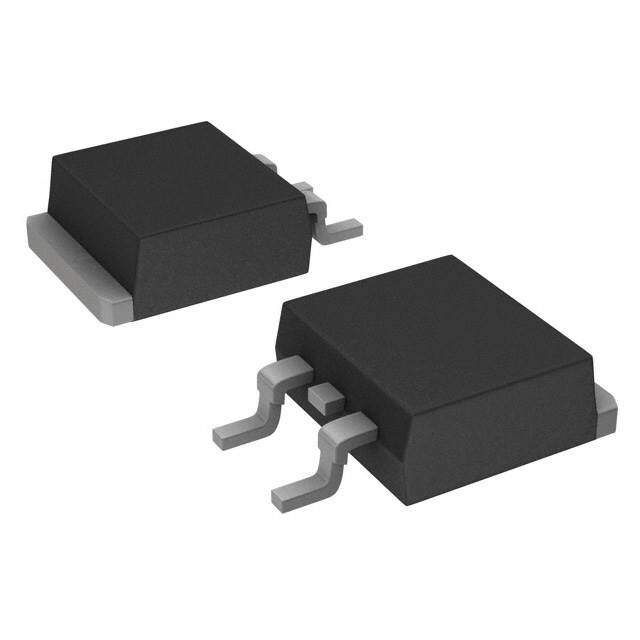
| 描述 | MOSFET N-CH 40V 80A TO-263 |
| 产品分类 | FET - 单 |
| FET功能 | 标准 |
| FET类型 | MOSFET N 通道,金属氧化物 |
| 品牌 | Renesas Electronics America |
| 数据手册 | |
| 产品图片 |
|
| 产品型号 | NP80N04PUG-E1B-AY |
| PCN组件/产地 | |
| PCN过时产品 | |
| rohs | 无铅 / 符合限制有害物质指令(RoHS)规范要求 |
| 产品系列 | - |
| 不同Id时的Vgs(th)(最大值) | 4V @ 250µA |
| 不同Vds时的输入电容(Ciss) | 7350pF @ 25V |
| 不同Vgs时的栅极电荷(Qg) | 135nC @ 10V |
| 不同 Id、Vgs时的 RdsOn(最大值) | 4.5 毫欧 @ 40A,10V |
| 供应商器件封装 | TO-263 |
| 其它名称 | NP80N04PUG-E1B-AYCT |
| 功率-最大值 | 1.8W |
| 包装 | 剪切带 (CT) |
| 安装类型 | 表面贴装 |
| 封装/外壳 | TO-263-3,D²Pak(2 引线+接片),TO-263AB |
| 标准包装 | 1 |
| 漏源极电压(Vdss) | 40V |
| 电流-连续漏极(Id)(25°C时) | 80A (Tc) |


- 商务部:美国ITC正式对集成电路等产品启动337调查
- 曝三星4nm工艺存在良率问题 高通将骁龙8 Gen1或转产台积电
- 太阳诱电将投资9.5亿元在常州建新厂生产MLCC 预计2023年完工
- 英特尔发布欧洲新工厂建设计划 深化IDM 2.0 战略
- 台积电先进制程称霸业界 有大客户加持明年业绩稳了
- 达到5530亿美元!SIA预计今年全球半导体销售额将创下新高
- 英特尔拟将自动驾驶子公司Mobileye上市 估值或超500亿美元
- 三星加码芯片和SET,合并消费电子和移动部门,撤换高东真等 CEO
- 三星电子宣布重大人事变动 还合并消费电子和移动部门
- 海关总署:前11个月进口集成电路产品价值2.52万亿元 增长14.8%


PDF Datasheet 数据手册内容提取
To our customers, Old Company Name in Catalogs and Other Documents On April 1st, 2010, NEC Electronics Corporation merged with Renesas Technology Corporation, and Renesas Electronics Corporation took over all the business of both companies. Therefore, although the old company name remains in this document, it is a valid Renesas Electronics document. We appreciate your understanding. Renesas Electronics website: http://www.renesas.com April 1st, 2010 Renesas Electronics Corporation Issued by: Renesas Electronics Corporation (http://www.renesas.com) Send any inquiries to http://www.renesas.com/inquiry.
Notice 1. All information included in this document is current as of the date this document is issued. Such information, however, is subject to change without any prior notice. Before purchasing or using any Renesas Electronics products listed herein, please confirm the latest product information with a Renesas Electronics sales office. Also, please pay regular and careful attention to additional and different information to be disclosed by Renesas Electronics such as that disclosed through our website. 2. Renesas Electronics does not assume any liability for infringement of patents, copyrights, or other intellectual property rights of third parties by or arising from the use of Renesas Electronics products or technical information described in this document. No license, express, implied or otherwise, is granted hereby under any patents, copyrights or other intellectual property rights of Renesas Electronics or others. 3. You should not alter, modify, copy, or otherwise misappropriate any Renesas Electronics product, whether in whole or in part. 4. Descriptions of circuits, software and other related information in this document are provided only to illustrate the operation of semiconductor products and application examples. You are fully responsible for the incorporation of these circuits, software, and information in the design of your equipment. Renesas Electronics assumes no responsibility for any losses incurred by you or third parties arising from the use of these circuits, software, or information. 5. When exporting the products or technology described in this document, you should comply with the applicable export control laws and regulations and follow the procedures required by such laws and regulations. You should not use Renesas Electronics products or the technology described in this document for any purpose relating to military applications or use by the military, including but not limited to the development of weapons of mass destruction. Renesas Electronics products and technology may not be used for or incorporated into any products or systems whose manufacture, use, or sale is prohibited under any applicable domestic or foreign laws or regulations. 6. Renesas Electronics has used reasonable care in preparing the information included in this document, but Renesas Electronics does not warrant that such information is error free. Renesas Electronics assumes no liability whatsoever for any damages incurred by you resulting from errors in or omissions from the information included herein. 7. Renesas Electronics products are classified according to the following three quality grades: “Standard”, “High Quality”, and “Specific”. The recommended applications for each Renesas Electronics product depends on the product’s quality grade, as indicated below. You must check the quality grade of each Renesas Electronics product before using it in a particular application. You may not use any Renesas Electronics product for any application categorized as “Specific” without the prior written consent of Renesas Electronics. Further, you may not use any Renesas Electronics product for any application for which it is not intended without the prior written consent of Renesas Electronics. Renesas Electronics shall not be in any way liable for any damages or losses incurred by you or third parties arising from the use of any Renesas Electronics product for an application categorized as “Specific” or for which the product is not intended where you have failed to obtain the prior written consent of Renesas Electronics. The quality grade of each Renesas Electronics product is “Standard” unless otherwise expressly specified in a Renesas Electronics data sheets or data books, etc. “Standard”: Computers; office equipment; communications equipment; test and measurement equipment; audio and visual equipment; home electronic appliances; machine tools; personal electronic equipment; and industrial robots. “High Quality”: Transportation equipment (automobiles, trains, ships, etc.); traffic control systems; anti-disaster systems; anti- crime systems; safety equipment; and medical equipment not specifically designed for life support. “Specific”: Aircraft; aerospace equipment; submersible repeaters; nuclear reactor control systems; medical equipment or systems for life support (e.g. artificial life support devices or systems), surgical implantations, or healthcare intervention (e.g. excision, etc.), and any other applications or purposes that pose a direct threat to human life. 8. You should use the Renesas Electronics products described in this document within the range specified by Renesas Electronics, especially with respect to the maximum rating, operating supply voltage range, movement power voltage range, heat radiation characteristics, installation and other product characteristics. Renesas Electronics shall have no liability for malfunctions or damages arising out of the use of Renesas Electronics products beyond such specified ranges. 9. Although Renesas Electronics endeavors to improve the quality and reliability of its products, semiconductor products have specific characteristics such as the occurrence of failure at a certain rate and malfunctions under certain use conditions. Further, Renesas Electronics products are not subject to radiation resistance design. Please be sure to implement safety measures to guard them against the possibility of physical injury, and injury or damage caused by fire in the event of the failure of a Renesas Electronics product, such as safety design for hardware and software including but not limited to redundancy, fire control and malfunction prevention, appropriate treatment for aging degradation or any other appropriate measures. Because the evaluation of microcomputer software alone is very difficult, please evaluate the safety of the final products or system manufactured by you. 10. Please contact a Renesas Electronics sales office for details as to environmental matters such as the environmental compatibility of each Renesas Electronics product. Please use Renesas Electronics products in compliance with all applicable laws and regulations that regulate the inclusion or use of controlled substances, including without limitation, the EU RoHS Directive. Renesas Electronics assumes no liability for damages or losses occurring as a result of your noncompliance with applicable laws and regulations. 11. This document may not be reproduced or duplicated, in any form, in whole or in part, without prior written consent of Renesas Electronics. 12. Please contact a Renesas Electronics sales office if you have any questions regarding the information contained in this document or Renesas Electronics products, or if you have any other inquiries. (Note 1) “Renesas Electronics” as used in this document means Renesas Electronics Corporation and also includes its majority- owned subsidiaries. (Note 2) “Renesas Electronics product(s)” means any product developed or manufactured by or for Renesas Electronics.
DATA SHEET MOS FIELD EFFECT TRANSISTOR NP80N04NUG, NP80N04PUG SWITCHING N-CHANNEL POWER MOS FET DESCRIPTION The NP80N04NUG and NP80N04PUG are N-channel MOS Field Effect Transistors designed for high current switching applications. ORDERING INFORMATION PART NUMBER LEAD PLATING PACKING PACKAGE Tube Note NP80N04NUG-S18-AY TO-262 (MP-25SK) typ. 1.8 g 50 p/tube Pure Sn (Tin) Note NP80N04PUG-E1B-AY Tape TO-263 (MP-25ZP) typ. 1.5 g NP80N04PUG-E2B-AY Note 1000 p/reel Note Pb-free (This product does not contain Pb in the external electrode.) FEATURES (TO-262) • Non logic level • Super low on-state resistance - NP80N04NUG RDS(on) = 4.8 mΩ MAX. (VGS = 10 V, ID = 40 A) - NP80N04PUG RDS(on) = 4.5 mΩ MAX. (VGS = 10 V, ID = 40 A) • High current rating (TO-263) ID(DC) = ±80 A • Low input capacitance Ciss = 4900 pF TYP. • Designed for automotive application and AEC-Q101 qualified The information in this document is subject to change without notice. Before using this document, please confirm that this is the latest version. Not all products and/or types are available in every country. Please check with an NEC Electronics sales representative for availability and additional information. Document No. D19799EJ1V0DS00 (1st edition) 2009 Date Published May 2009 NS Printed in Japan
NP80N04NUG, NP80N04PUG ABSOLUTE MAXIMUM RATINGS (TA = 25°C) Drain to Source Voltage (VGS = 0 V) VDSS 40 V Gate to Source Voltage (VDS = 0 V) VGSS ±20 V Drain Current (DC) (TC = 25°C) ID(DC) ±80 A Drain Current (pulse) Note1 ID(pulse) ±300 A Total Power Dissipation (TC = 25°C) PT1 115 W Total Power Dissipation (TA = 25°C) PT2 1.8 W Channel Temperature Tch 175 °C Storage Temperature Tstg −55 to +175 °C Repetitive Avalanche Current Note2 IAR 37 A Repetitive Avalanche Energy Note2 EAR 137 mJ Notes 1. PW ≤ 10 μs, Duty Cycle ≤ 1% 2. Tch ≤ 150°C, RG = 25 Ω THERMAL RESISTANCE Channel to Case Thermal Resistance Rth(ch-C) 1.30 °C/W Channel to Ambient Thermal Resistance Rth(ch-A) 83.3 °C/W 2 Data Sheet D19799EJ1V0DS
NP80N04NUG, NP80N04PUG ELECTRICAL CHARACTERISTICS (TA = 25°C) CHARACTERISTICS SYMBOL TEST CONDITIONS MIN. TYP. MAX. UNIT Zero Gate Voltage Drain Current IDSS VDS = 40 V, VGS = 0 V 1 μA Gate Leakage Current IGSS VGS = ±20 V, VDS = 0 V ±100 nA Gate to Source Threshold Voltage VGS(th) VDS = VGS, ID = 250 μA 2.0 4.0 V Note Forward Transfer Admittance | yfs | VDS = 5 V, ID = 35 A 25 50 S Drain to Source On-state Resistance Note RDS(on) VGS = 10 V, NP80N04NUG 3.6 4.8 mΩ ID = 40 A NP80N04PUG 3.2 4.5 mΩ Input Capacitance Ciss VDS = 25 V, 4900 7350 pF Output Capacitance Coss VGS = 0 V, 480 720 pF Reverse Transfer Capacitance Crss f = 1 MHz 310 560 pF Turn-on Delay Time td(on) VDD = 20 V, ID = 40 A, 32 70 ns Rise Time tr VGS = 10 V, 23 58 ns Turn-off Delay Time td(off) RG = 0 Ω 65 130 ns Fall Time tf 11 28 ns Total Gate Charge QG VDD = 32 V, 90 135 nC Gate to Source Charge QGS VGS = 10 V, 21 nC Gate to Drain Charge QGD ID = 80 A 31 nC Note Body Diode Forward Voltage VF(S-D) IF = 80 A, VGS = 0 V 0.92 1.5 V Reverse Recovery Time trr IF = 80 A, VGS = 0 V, 40 ns Reverse Recovery Charge Qrr di/dt = 100 A/μs 44 nC Note Pulsed test TEST CIRCUIT 1 AVALANCHE CAPABILITY TEST CIRCUIT 2 SWITCHING TIME D.U.T. D.U.T. PG. RG =5 205 Ω Ω LVDD PG. RG RVDLD VWaGveS FormVG0S10% VGS 90% VGS = 20 → 0 V VDS 90% 90% BVDSS V0GS VDS V0DS 10% 10% IAS Wave Form ID VDS τ td(on) tr td(off) tf VDD τ = 1 μ s ton toff Duty Cycle ≤ 1% Starting Tch TEST CIRCUIT 3 GATE CHARGE D.U.T. IG = 2 mA RL PG. 50 Ω VDD Data Sheet D19799EJ1V0DS 3
NP80N04NUG, NP80N04PUG TYPICAL CHARACTERISTICS (TA = 25°C) DERATING FACTOR OF FORWARD BIAS TOTAL POWER DISSIPATION vs. SAFE OPERATING AREA CASE TEMPERATURE 120 125 % wer - 100 n - W 100 d Po 80 patio e si 75 Rat Dis of 60 er ge ow 50 a 40 P cent otal dT - Per 200 0 25 50 75 100 125 150 175 P - TT 250 0 25 50 75 100 125 150 175 TC - Case Temperature - °C TC - Case Temperature - °C FORWARD BIAS SAFE OPERATING AREA 1000 nt - A 100 R(DVS(GonS) =L i1IimDi0t( DVeCd)) DCID(pulse) PW1i = 1i00 μs I - Drain CurreD 101 TC = 25°C Power Dissipation LimitSeedcondary Brakedownm Lsiimited 1i0 msi Single Pulse 0.1 0.1 1 10 100 VDS - Drain to Source Voltage - V TRANSIENT THERMAL RESISTANCE vs. PULSE WIDTH 1000 W C/ °e - 100 Rth(ch-A) = 83.3°C/W c n a st esi 10 R al erm Rth(ch-C) = 1.30°C/W h 1 T nt e si n a 0.1 Tr r - th(t) 0.01 1 m 10 m 100 m 1 10 1S00in gle Pulse100 0 PW - Pulse Width - s 4 Data Sheet D19799EJ1V0DS
NP80N04NUG, NP80N04PUG DRAIN CURRENT vs. DRAIN CURRENT vs. DRAIN TO SOURCE VOLTAGE DRAIN TO SOURCE VOLTAGE 400 400 VGS = 10 V VGS = 10 V 350 350 Pulsed Pulsed A 300 A 300 Current - 220500 Current - 220500 Drain 150 Drain 150 I - D 10500 NP80N04NUG I - D 10500 NP80N04PUG 0 0 0 0.5 1 1.5 2 0 0.5 1 1.5 2 VDS - Drain to Source Voltage - V VDS - Drain to Source Voltage - V FORWARD TRANSFER CHARACTERISTICS GATE TO SOURCE THRESHOLD VOLTAGE vs. CHANNEL TEMPERATURE V 1000 e - 5 g 100 Tch = −55°C Volta 4 A 10 −25°C d Drain Current - 0.11 1112572750555°°°°°CCCCC ource Threshol 23 I - D 0.00.000.000111 VPDuSls =e d10 V - Gate to SS(th) 01 VIDD =S =2 5V0G μSA 0 1 2 3 4 5 6 VG -75 -25 25 75 125 175 225 VGS - Gate to Source Voltage - V Tch - Channel Temperature - °C FORWARD TRANSFER ADMITTANCE vs. DRAIN CURRENT S 100 nce - Tch = −55°C a −25°C mitt 25°C Ad 75°C er 125°C 150°C nsf 10 175°C a Tr d ar w or F y | - fs VPuDSls =e d5 V | 10.1 1 10 100 ID - Drain Current - A Data Sheet D19799EJ1V0DS 5
NP80N04NUG, NP80N04PUG DRAIN TO SOURCE ON-STATE RESISTANCE vs. DRAIN TO SOURCE ON-STATE RESISTANCE vs. DRAIN CURRENT DRAIN CURRENT Ω Ω m 10 m 10 e - VGS = 10 V e - VGS = 10 V nc Pulsed nc Pulsed sta 8 sta 8 si si e e R R ate 6 ate 6 st st n- n- O O e 4 e 4 c c ur ur o o S S n to 2 n to 2 Drai NP80N04NUG Drai NP80N04PUG - DS(on) 0 1 10 100 1000 - DS(on) 0 1 10 100 1000 R R ID - Drain Current - A ID - Drain Current - A DRAIN TO SOURCE ON-STATE RESISTANCE vs. DRAIN TO SOURCE ON-STATE RESISTANCE vs. GATE TO SOURCE VOLTAGE GATE TO SOURCE VOLTAGE Ω Ω m 10 m 10 e - ID = 40 A e - ID = 40 A nc Pulsed nc Pulsed sta 8 sta 8 si si e e R R ate 6 ate 6 st st n- n- O O e 4 e 4 c c ur ur o o S S n to 2 n to 2 Drai NP80N04NUG Drai NP80N04PUG - DS(on) 0 0 4 8 12 16 20 - DS(on) 0 0 4 8 12 16 20 R R VGS - Gate to Source Voltage - V VGS - Gate to Source Voltage - V DRAIN TO SOURCE ON-STATE RESISTANCE vs. DRAIN TO SOURCE ON-STATE RESISTANCE vs. CHANNEL TEMPERATURE CHANNEL TEMPERATURE Ω Ω m 10 m 10 e - VGS = 10 V e - VGS= 10 V stanc 8 IPDu =ls 4e0d A stanc 8 IPDu =ls 4e0d A si si e e R R ate 6 ate 6 st st n- n- O O e 4 e 4 c c ur ur o o S S n to 2 n to 2 Drai NP80N04NUG Drai NP80N04PUG - DS(on) 0-75 -25 25 75 125 175 225 - DS(on) 0-75 -25 25 75 125 175 225 R R Tch - Channel Temperature - °C Tch - Channel Temperature - °C 6 Data Sheet D19799EJ1V0DS
NP80N04NUG, NP80N04PUG CAPACITANCE vs. DRAIN TO SOURCE VOLTAGE SWITCHING CHARACTERISTICS 100000 1000 ce - pF me - ns citan 10000 Ciss ng Ti 100 td(off) Capa witchi td(on) C, C, C - issossrss 1010000 Vf =G S1 = M 0H Vz CCorssss t, t, t, t - Sd(on)rd(off)f 101 VVRDGGDS === 0 21 Ω00 VVtr tf 0.01 0.1 1 10 100 0.1 1 10 100 VDS - Drain to Source Voltage - V ID - Drain Current - A DYNAMIC INPUT/OUTPUT CHARACTERISTICS SOURCE TO DRAIN DIODE FORWARD VOLTAGE 35 14 1000 V V Voltage - 2350 VDD = 23082 VVV 1102 Voltage - urrent - A 100 10 V urce 20 8 urce ard C 10 VGS = 0 V o o w ain to S 1105 VGS 46 ain to S ode For 1 Dr Dr Di V - DS 05 0 20 40VDS 60 ID8 =0 80 A10002 V - DS I - F 0.00.11 0 0.2 0.4 0.6 0.8 1 P1.u2lsed1.4 QG - Gate Charge - nC VF(S-D) - Source to Drain Voltage - V REVERSE RECOVERY TIME vs. DIODE FORWARD CURRENT 100 s n e - m Ti y er v o c e R e s er v e R t - rr 10 dViG/dS t= = 0 1 V00 A/μs 0.1 1 10 100 IF - Diode Forward Current - A Data Sheet D19799EJ1V0DS 7
NP80N04NUG, NP80N04PUG PACKAGE DRAWINGS (Unit: mm) TO-262 (MP-25SK) TO-263 (MP-25ZP) 3 10.0±0.2 ±1.20.3 4.45±0.21.3±0.2 No plating 170.8.08 ±M0IN.3. 1.35 ±0. 4.45 ±0.21.3 ±0.2 4 3 P. 4 1 2 3 ±8.90.2 ±10.10. 0.3 8.0 TY 0.5 9.15 ±0.3 25 ±0.5 0to.0 02.525 0.3 1.27±0.2 ±3.1 15. ± 13.7 0.8±0.1 0.6 ±0.2 0.5±0.2 2.5±0.2 0.75 ±0.2 2.54 0 to 8˚ 0.25 2.54 TYP. 2.54 TYP. 0.25 ± 1. Gate 1 2 3 54 2. Drain 2.5 1. Gate 2. 3. Source 2. Drain 4. Fin (Drain) 3. Source 4. Fin (Drain) EQUIVALENT CIRCUIT Drain Body Gate Diode Source Remark Strong electric field, when exposed to this device, can cause destruction of the gate oxide and ultimately degrade the device operation. Steps must be taken to stop generation of static electricity as much as possible, and quickly dissipate it once, when it has occurred. 8 Data Sheet D19799EJ1V0DS
NP80N04NUG, NP80N04PUG TAPE INFORMATION (NP80N04PUG) There are two types (-E1B, -E2B) of taping depending on the direction of the device. Draw-out side Reel side −E1B TYPE −E2B TYPE MARKING INFORMATION NE C Pb-free plating marking 80N04 Abbreviation of part number UG Lot code RECOMMENDED SOLDERING CONDITIONS These products should be soldered and mounted under the following recommended conditions. For soldering methods and conditions other than those recommended below, please contact an NEC Electronics sales representative. For technical information, see the following website. Semiconductor Device Mount Manual (http://www.necel.com/pkg/en/mount/index.html) Recommended Soldering Method Soldering Conditions Condition Symbol Infrared reflow Maximum temperature (Package's surface temperature): 260°C or below IR60-00-3 NP80N04PUG Time at maximum temperature: 10 seconds or less Time of temperature higher than 220°C: 60 seconds or less Preheating time at 160 to 180°C: 60 to 120 seconds Maximum number of reflow processes: 3 times Maximum chlorine content of rosin flux (percentage mass): 0.2% or less Wave soldering Maximum temperature (Solder temperature): 260°C or below THDWS NP80N04NUG Time: 10 seconds or less Maximum chlorine content of rosin flux: 0.2% (wt.) or less Partial heating Maximum temperature (Pin temperature): 350°C or below P350 NP80N04NUG, Time (per side of the device): 3 seconds or less NP80N04PUG Maximum chlorine content of rosin flux: 0.2% (wt.) or less Caution Do not use different soldering methods together (except for partial heating). Data Sheet D19799EJ1V0DS 9
NP80N04NUG, NP80N04PUG • The information in this document is current as of May, 2009. The information is subject to change without notice. For actual design-in, refer to the latest publications of NEC Electronics data sheets, etc., for the most up-to-date specifications of NEC Electronics products. Not all products and/or types are available in every country. Please check with an NEC Electronics sales representative for availability and additional information. • No part of this document may be copied or reproduced in any form or by any means without the prior written consent of NEC Electronics. NEC Electronics assumes no responsibility for any errors that may appear in this document. • NEC Electronics does not assume any liability for infringement of patents, copyrights or other intellectual property rights of third parties by or arising from the use of NEC Electronics products listed in this document or any other liability arising from the use of such products. No license, express, implied or otherwise, is granted under any patents, copyrights or other intellectual property rights of NEC Electronics or others. • Descriptions of circuits, software and other related information in this document are provided for illustrative purposes in semiconductor product operation and application examples. The incorporation of these circuits, software and information in the design of a customer's equipment shall be done under the full responsibility of the customer. NEC Electronics assumes no responsibility for any losses incurred by customers or third parties arising from the use of these circuits, software and information. • While NEC Electronics endeavors to enhance the quality and safety of NEC Electronics products, customers agree and acknowledge that the possibility of defects thereof cannot be eliminated entirely. In addition, NEC Electronics products are not taken measures to prevent radioactive rays in the product design. When customers use NEC Electronics products with their products, customers shall, on their own responsibility, incorporate sufficient safety measures such as redundancy, fire-containment and anti-failure features to their products in order to avoid risks of the damages to property (including public or social property) or injury (including death) to persons, as the result of defects of NEC Electronics products. • NEC Electronics products are classified into the following three quality grades: "Standard", "Special" and "Specific". The "Specific" quality grade applies only to NEC Electronics products developed based on a customer- designated "quality assurance program" for a specific application. The recommended applications of an NEC Electronics product depend on its quality grade, as indicated below. Customers must check the quality grade of each NEC Electronics product before using it in a particular application. "Standard": Computers, office equipment, communications equipment, test and measurement equipment, audio and visual equipment, home electronic appliances, machine tools, personal electronic equipment and industrial robots. "Special": Transportation equipment (automobiles, trains, ships, etc.), traffic control systems, anti-disaster systems, anti-crime systems, safety equipment and medical equipment (not specifically designed for life support). "Specific": Aircraft, aerospace equipment, submersible repeaters, nuclear reactor control systems, life support systems and medical equipment for life support, etc. The quality grade of NEC Electronics products is "Standard" unless otherwise expressly specified in NEC Electronics data sheets or data books, etc. If customers wish to use NEC Electronics products in applications not intended by NEC Electronics, they must contact an NEC Electronics sales representative in advance to determine NEC Electronics' willingness to support a given application. (Note) (1) "NEC Electronics" as used in this statement means NEC Electronics Corporation and also includes its majority-owned subsidiaries. (2) "NEC Electronics products" means any product developed or manufactured by or for NEC Electronics (as defined above). M8E0904E