ICGOO在线商城 > 光电元件 > 显示器模块 - LCD,OLED 字符和数字 > NHD-0216SZW-BY5
 Datasheet下载
- 型号: NHD-0216SZW-BY5
- 制造商: Newhaven Display
- 库位|库存: xxxx|xxxx
- 要求:
| 数量阶梯 | 香港交货 | 国内含税 |
| +xxxx | $xxxx | ¥xxxx |
查看当月历史价格
查看今年历史价格
NHD-0216SZW-BY5产品简介:
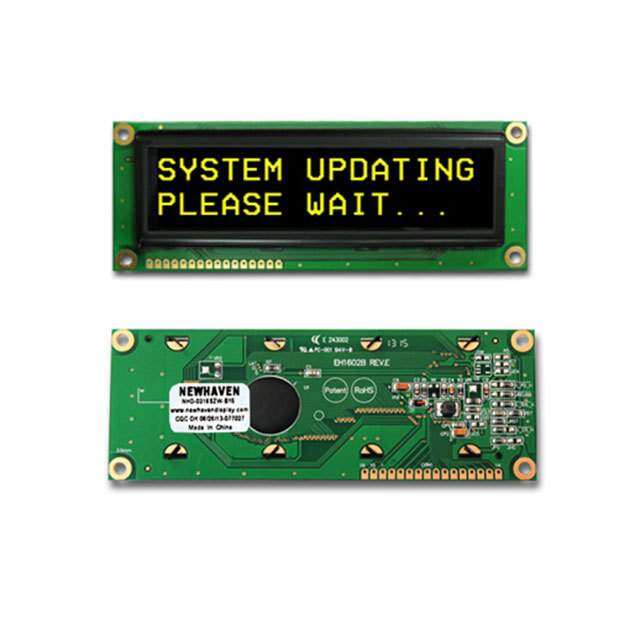
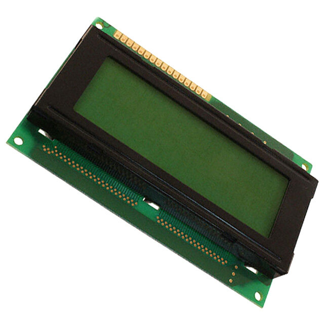
ICGOO电子元器件商城为您提供NHD-0216SZW-BY5由Newhaven Display设计生产,在icgoo商城现货销售,并且可以通过原厂、代理商等渠道进行代购。 NHD-0216SZW-BY5价格参考。Newhaven DisplayNHD-0216SZW-BY5封装/规格:显示器模块 - LCD,OLED 字符和数字, Character LCD Display Module 无源 5 x 8 点 OLED 无背光 并行/串行 122.00mm x 44.00mm x 10.00mm。您可以下载NHD-0216SZW-BY5参考资料、Datasheet数据手册功能说明书,资料中有NHD-0216SZW-BY5 详细功能的应用电路图电压和使用方法及教程。
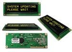
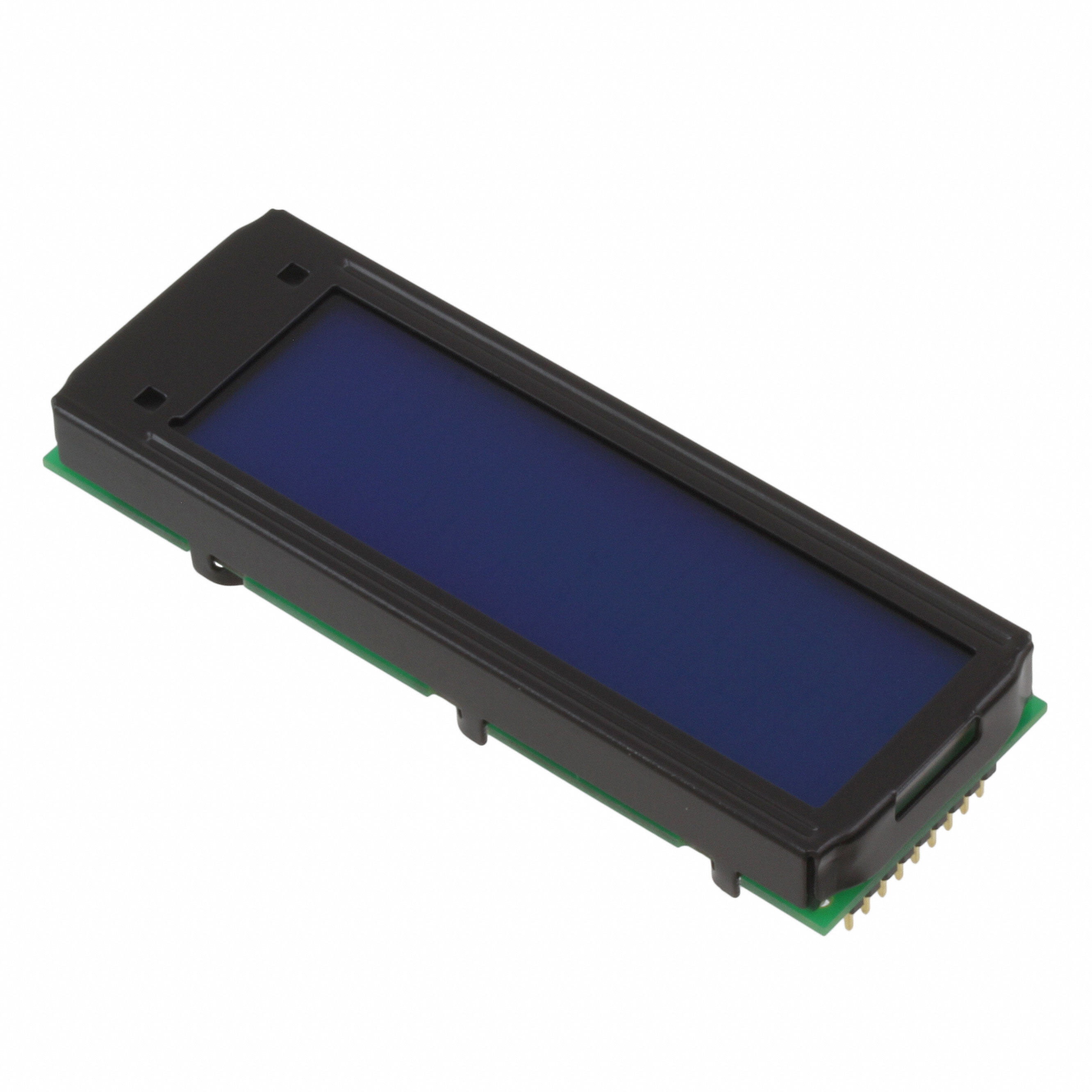
Newhaven Display Intl品牌的NHD-0216SZW-BY5属于字符型液晶显示器(LCD)模块,广泛应用于各类小型电子设备中,适用于需要显示简单文本或字符信息的场景。

该型号为2行×16字符显示,采用STN蓝色液晶屏,带背光设计,具有良好的可视性和低功耗特性,适合在低亮度环境下使用。其工业级的工作温度范围也使其适应性更强。

典型应用场景包括:

1. 工业控制设备:如PLC、HMI界面、传感器显示模块,用于显示状态信息或操作提示。
2. 医疗仪器:如血糖仪、血压计、便携式监护设备,用于显示测量结果和操作指引。
3. 消费电子产品:如智能电表、电子秤、温湿度计等,用于显示实时数据。
4. 安防设备:如门禁控制器、报警系统,用于显示状态和提示信息。
5. 测试测量仪器:如万用表、示波器等,用于显示参数和操作反馈。

该LCD模块接口通用,常采用4位或8位并行接口,便于与MCU连接,适合嵌入式系统开发,广泛用于需要可靠显示解决方案的中低端设备中。
| 参数 | 数值 |
| 产品目录 | |
| 描述 | DISPLAY OLED CHAR 2X16 YLWOLED显示器和配件 OLED 2x16 Yellow 122.0 x 44.0 x 10 |
| 产品分类 | |
| 品牌 | Newhaven Display |
| 产品手册 | |
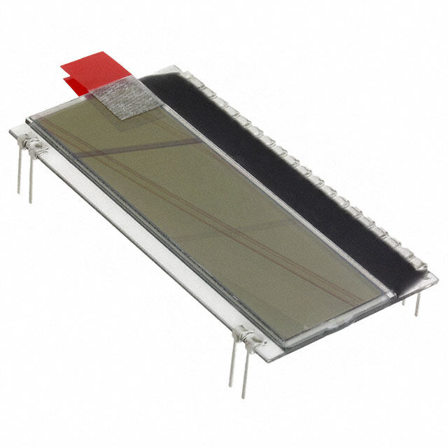
| 产品图片 |
|
| rohs | 符合RoHS无铅 / 符合限制有害物质指令(RoHS)规范要求 |
| 产品系列 | OLED显示器和配件,Newhaven Display NHD-0216SZW-BY5- |
| 数据手册 | |
| 产品型号 | NHD-0216SZW-BY5 |
| 产品 | OLED Display Modules |
| 产品培训模块 | http://www.digikey.cn/PTM/IndividualPTM.page?site=cn&lang=zhs&ptm=25399http://www.digikey.cn/PTM/IndividualPTM.page?site=cn&lang=zhs&ptm=25934 |
| 产品种类 | OLED显示器和配件 |
| 其它名称 | NHD0216SZWBY5 |
| 其它有关文件 | |
| 可视范围 | 99.00mm 长 x 24.00mm 宽 |
| 商标 | Newhaven Display |
| 外形尺寸LxWxH | 122.00mm x 44.00mm x 10.00mm |
| 字符大小 | 8.90mm 高 x 4.74mm 宽 |
| 字符数 | 32 |
| 字符格式 | 5 x 8 点 |
| 工作温度 | -40°C ~ 80°C |
| 工作电流 | 43 mA |
| 工作电源电压 | 3 V/5 V |
| 接口 | Parallel/3-Wire SPI |
| 文字颜色 | 黄 |
| 显示格式 | 16 x 2 |
| 显示模式 | 无源 |
| 显示类型 | OLED |
| 显示角 | 80 deg |
| 最大工作温度 | + 80 C |
| 最小工作温度 | - 40 C |
| 标准包装 | 100 |
| 点尺寸 | 0.90mm 宽 x 1.06mm 高 |
| 照明颜色 | Yellow |
| 电压-电源 | 3 V ~ 5.3 V |
| 背光 | 无背光 |
| 背景颜色 | 黑 |
| 观察区域-宽x高 | 99 mm x 24 mm |
| 设计资源 | http://www.eewiki.net/display/Motley/Bit-bang+Serial+Control+of+Newhaven+OLED+Character+Display#Bit-bangSerialControlofNewhavenOLEDCharacterDisplay-Displayinterfaceconfiguration-parallelorserial?http://www.eewiki.net/display/Motley/Bit-bang+Serial+Control+of+Newhaven+OLED+Character+Display |


- 商务部:美国ITC正式对集成电路等产品启动337调查
- 曝三星4nm工艺存在良率问题 高通将骁龙8 Gen1或转产台积电
- 太阳诱电将投资9.5亿元在常州建新厂生产MLCC 预计2023年完工
- 英特尔发布欧洲新工厂建设计划 深化IDM 2.0 战略
- 台积电先进制程称霸业界 有大客户加持明年业绩稳了
- 达到5530亿美元!SIA预计今年全球半导体销售额将创下新高
- 英特尔拟将自动驾驶子公司Mobileye上市 估值或超500亿美元
- 三星加码芯片和SET,合并消费电子和移动部门,撤换高东真等 CEO
- 三星电子宣布重大人事变动 还合并消费电子和移动部门
- 海关总署:前11个月进口集成电路产品价值2.52万亿元 增长14.8%

PDF Datasheet 数据手册内容提取
NHD-0216SZW-BY5 OLED Display Module NHD- Newhaven Display 0216- 2 Lines x 16 Characters SZW- OLED B- Model Y- Emitting Color: Yellow 5- +5V Power Supply Newhaven Display International, Inc. 2661 Galvin Ct. Elgin IL, 60124 Ph: 847-844-8795 Fax: 847-844-8796 www.newhavendisplay.com nhtech@newhavendisplay.com nhsales@newhavendisplay.com
Document Revision History Revision Date Description Changed by 0 4/1/2011 Initial Product Release - 1 7/12/2011 Serial interface information updated AK 2 10/18/2011 Jumper selections updated AK 3 3/26/2012 Jumper selections updated AK 4 2/8/2013 Optical characteristics and mechanical drawing updated. JN 5 9/7/2013 Photo of jumpers (solder pads) added AK 6 5/27/16 Jumper Pad Picture Updated SB 7 12/21/16 Mechanical Drawing & Supply Current Updated SB Functions and Features • 2 lines x 16 characters • Built-in LCD comparable controller • Parallel or serial MPU interface (Default 6800 MPU parallel) • +3.0V or +5.0V Power Supply • RoHS compliant • Size compatible to NHD-0216SZ series Character LCDs [2]
Mechanical Drawing 1 2 3 4 5 6 Y Rev Description Date 122.0 0.5 R 3.5 115.0 8.2 105.6 A 11.5 99.0(VA) A A 10.0MAX 2.9 8 0.51 14.95 91.14 (AA) 3.5 4.7 1 T ) E ) A B 4.00.5 34.2 24.0(VA 8.98 (A I 37.0 Pin Assignment B 4 1 1 Vss R 2 Vdd 3 NC 2.0 P 16-1.0 PTH 4-O3.5 PTH 1.6 4 RS 10.98 P2.54*15=38.1 5 4-O6.5 PAD 2. 5 R/W 6 E O 7 DB0 C C 8 DB1 9 DB2 R 5.76 10 DB3 4.74 0.96 11 DB4 0.9 P 12 DB5 13 DB6 1.121.06 0 14 DB7 D 10.088.9 15 NC D 16 NC Notes: Unit 1. Display Type: 16x2 Character OLED mm 2. Emitting Color: Yellow DOT SIZE SCALE 5/1 Gen. Tol. Date Part Number: 3. Interface: Parallel 6800/8080 or SPI ±0.3 12/21/16 NHD-0216SZW-BY5 1 2 3 4 5 6 The information contained herein is the exclusive property of Newhaven Display International, Inc. and shall not be copied, reproduced, and/or disclosed in any format without permission. [3]
Pin Description Parallel Interface (default): Pin No. Symbol External Function Description Connection 1 V Power Supply Ground SS 2 V Power Supply Supply Voltage for OLED and logic DD 3 NC - No Connect 4 RS MPU Register Select signal. RS=0: Command, RS=1: Data 5 R/W MPU Read/Write select signal, R/W=1: Read R/W: =0: Write 6 E MPU Operation Enable signal. Falling edge triggered. 7-10 DB0 – DB3 MPU Four low order bi-directional three-state data bus lines. These four are not used during 4-bit operation. 11-14 DB4 – DB7 MPU Four high order bi-directional three-state data bus lines. 15 NC - No Connect 16 NC - No Connect Serial Interface: Pin No. Symbol External Function Description Connection 1 V Power Supply Ground SS 2 V Power Supply Supply Voltage for OLED and logic DD 3-11 NC - No Connect 12 SCL MPU Serial Clock signal 13 SDO MPU Serial Data output signal 14 SDI MPU Serial Data input signal 15 NC - No Connect 16 /CS MPU Active LOW Chip Select signal Jumper Selections MPU Interface L_PS_H J80_J68 L_SHL_H L_CS_H JCS 6800-MPU Parallel (default) H J68 H L X 8080-MPU Parallel H J80 H L X Serial MPU L X H Open Short X = Don’t care [4]
Wiring Diagrams [5]
Electrical Characteristics Item Symbol Condition Min. Typ. Max. Unit Operating Temperature Range T Absolute Max -40 - +80 ⁰C OP Storage Temperature Range T Absolute Max -40 - +80 ⁰C ST Supply Voltage V - 3.0 5.0 5.3 V DD Supply Current I T =25°C, V =5.0V 56 62 65 mA DD OP DD “H” Level input V - 0.9*V - V V IH DD DD “L” Level input V - V - 0.1*V V IL SS DD “H” Level output V - 0.8*V - V V OH DD DD “L” Level output V - V - 0.2*V V OL SS DD Optical Characteristics Item Symbol Condition Min. Typ. Max. Unit Top ϕY+ 80 - - ⁰ Optimal Bottom ϕY- 80 - - ⁰ Viewing Left θX- 80 - - ⁰ Angles Right θX+ 80 - - ⁰ Contrast Ratio CR - 2000:1 - - - Rise T - 10 - us Response Time R - Fall T - 10 - us F Brightness 50% checkerboard 70 90 - cd/m2 Lifetime TOP=25°C 100,000 - - Hrs 50% checkerboard Note: Lifetime at typical temperature is based on accelerated high-temperature operation. Lifetime is tested at average 50% pixels on and is rated as Hours until Half-Brightness. The Display OFF command can be used to extend the lifetime of the display. Luminance of active pixels will degrade faster than inactive pixels. Residual (burn-in) images may occur. To avoid this, every pixel should be illuminated uniformly. [6]
Table of Commands Code Max Instruction Description Execution RS R/W DB7 DB6 DB5 DB4 DB3 DB2 DB1 DB0 Time Clears entire display. Clear Display 0 0 0 0 0 0 0 0 0 1 2ms Does not change DDRAM address. Sets DDRAM Address to 0x00. Return 0 0 0 0 0 0 0 0 1 0 Returns shifted 600us Home display to original position. Sets cursor to auto Entry Mode Increment or 0 0 0 0 0 0 0 1 I/D S 600us Set Decrement, and sets display shift. Sets Display (D) ON/OFF. Display Sets Cursor (C) ON/OFF 0 0 0 0 0 0 1 D C B 600us ON/OFF. control Sets Blinking (B) of cursor ON/OFF. Moves cursor & Cursor/Displ shifts display 0 0 0 0 0 1 S/C R/L 0 0 600us ay Shift without changing DDRAM contents. Set interface data Function Set 0 0 0 0 1 DL 1 0 FT1 FT0 length. 600us Select Font Table. Set CGRAM Move to CGRAM 0 0 0 1 ACG5 ACG4 ACG3 ACG2 ACG1 ACG0 600us address address. Set DDRAM Move to DDRAM 0 0 1 ADD6 ADD5 ADD4 ADD3 ADD2 ADD1 ADD0 600us address address. Read Busy Read Busy Flag Flag & 0 1 BF AC6 AC5 AC4 AC3 AC2 AC1 AC0 (BF) and Address 600us Address Counter. Write data Write data to to CGRAM 1 0 Write Data 600us CGRAM or DDRAM or DDRAM Read data from Read data from 1 1 Read Data 600us CGRAM or CGRAM or DDRAM DDRAM [7]
Instruction Descriptions When an instruction is being executed, only the Busy Flag read instruction can be performed. During execution of an instruction, the Busy Flag = “1”. When BF = “0” instructions can be sent to the controller. Clear Display RS R/W DB7 DB6 DB5 DB4 DB3 DB2 DB1 DB0 0 0 0 0 0 0 0 0 0 1 This instruction is used to clear the display by writing 0x20 in all DDRAM addresses. This instruction does not change the DDRAM Address. Return Home RS R/W DB7 DB6 DB5 DB4 DB3 DB2 DB1 DB0 0 0 0 0 0 0 0 0 1 0 This instruction is used to set the DDRAM Address to 0x00 and shifts the display back to the original state. The cursor (if on) will be at the first line’s left-most character. The DDRAM contents on the display do not change. Entry Mode Set RS R/W DB7 DB6 DB5 DB4 DB3 DB2 DB1 DB0 0 0 0 0 0 0 0 1 I/D S I/D = Increment/Decrement When I/D = “1”, the DDRAM or CGRAM Address with automatically increment when a character code is written into or read from the DDRAM or CGRAM. The auto-increment will move the cursor one character space to the right. When I/D = “0”, the DDRAM or CGRAM Address with automatically decrement when a character code is written into or read from the DDRAM or CGRAM. The auto-decrement will move the cursor one character space to the left. S = Shift Entire Display When S = “1”, the entire display is shifted to the right (when I/D = “0”) or left (when I/D = “1”). I/D=1, S=1 I/D=0, S=1 [8]
Display ON/OFF RS R/W DB7 DB6 DB5 DB4 DB3 DB2 DB1 DB0 0 0 0 0 0 0 1 D C B D = Display ON/OFF When D = “1”, the display is turned ON. When D = “0”, the display is turned OFF. Contents in DDRAM are not changed. C = Cursor ON/OFF When C = “1”, the cursor is displayed. The cursor is displayed as 5 dots on the 8th line of a character. When C = “0”, the cursor is OFF. B = Blinking Cursor When B = “1”, the entire character specified by the cursor blinks at a speed of 409.6ms intervals. When B = “0”, the character does not blink, the cursor remains on. Cursor/Display Shift RS R/W DB7 DB6 DB5 DB4 DB3 DB2 DB1 DB0 0 0 0 0 0 1 S/C R/L 0 0 S/C R/L Shift Function 0 0 Shifts the cursor position to the left (AC is decremented by 1). 0 1 Shifts the cursor position to the right (AC is incremented by 1). 1 0 Shifts the entire display to the left. The cursor follows the display shift. 1 1 Shifts the entire display to the right. The cursor follows the display shift. When the display is shifted repeatedly, each line moves only horizontally. The second line display does not shift into the first line. The Address Counter does not change during a Display Shift. Function Set RS R/W DB7 DB6 DB5 DB4 DB3 DB2 DB1 DB0 0 0 0 0 1 DL 1 0 FT1 FT0 DL = Interface Data Length When DL = “1”, the data is sent or received in 8-bit length via DB7...DB0. When DL = “0”, the data is sent or received in 4-bit length via DB7...DB4. When the 4-bit data length is used, the data must be sent or received in two consecutive writes/reads to combine the data into full 8-bits. FT1, FT0 = Font Table Selection FT1 FT0 Font Table 0 0 English / Japanese 0 1 Western European #1 1 0 English / Russian 1 1 Western European #2 Note: Changing the font table during operation will immediately change any data currently on the display to the corresponding character on the newly selected font table. [9]
Set CGRAM Address RS R/W DB7 DB6 DB5 DB4 DB3 DB2 DB1 DB0 0 0 0 1 ACG5 ACG4 ACG3 ACG2 ACG1 ACG0 This instruction is used to set the CGRAM address into the Address Counter. Data can then be written to or read from the CGRAM locations. See section: “How to use CGRAM”. ACG5...ACG0 is the binary CGRAM address. Set DDRAM Address RS R/W DB7 DB6 DB5 DB4 DB3 DB2 DB1 DB0 0 0 1 ADD6 ADD5 ADD4 ADD3 ADD2 ADD1 ADD0 This instruction is used to set the DDRAM address into the Address Counter. Data can then be written to or read from the DDRAM locations. ADD6...ADD0 is the binary DDRAM address. Line 1 = Address 0x00 through 0x0F Line 2 = Address 0x40 through 0x4F 1 2 3 4 5 6 7 8 9 10 11 12 13 14 15 16 00 01 02 03 04 05 06 07 08 09 0A 0B 0C 0D 0E 0F 40 41 42 43 44 45 46 47 48 49 4A 4B 4C 4D 4E 4F Read Busy Flag and Address Counter RS R/W DB7 DB6 DB5 DB4 DB3 DB2 DB1 DB0 0 1 BF AC6 AC5 AC4 AC3 AC2 AC1 AC0 This instruction is used to read the Busy Flag (BF) to indicate if the display controller is performing an internal operation. The Address Counter is read simultaneously with checking the Busy Flag. When BF = “1”, the controller is busy and the next instruction will be ignored. When BF = “0”, the controller is not busy and is ready to accept instructions. AC6...AC0 is the binary location of either the CGRAM or DDRAM current address. Write Data to CGRAM or DDRAM RS R/W DB7 DB6 DB5 DB4 DB3 DB2 DB1 DB0 1 0 Write Data This instruction is used to write 8-bits of data to the CGRAM or DDRAM at the current address counter. After the write is complete, the address is automatically incremented or decremented by 1 according to the Entry Mode. Read Data from CGRAM or DDRAM RS R/W DB7 DB6 DB5 DB4 DB3 DB2 DB1 DB0 1 1 Read Data This instruction is used to read 8-bits of data to the CGRAM or DDRAM at the current address counter. After the read is complete, the address is automatically incremented or decremented by 1 according to the Entry Mode. The Set CGRAM Address or Set DDRAM Address Instruction must be executed before this instruction can be performed, otherwise the first Read Data will not be valid. [10]
MPU Interface When DL is set for 8-bit mode, the display interfaces with the MPU with DB7...DB0 (DB7 is the MSB). When DL is set for 4-bit mode, the display interfaces with the MPU with only DB7...DB4 (DB7 is the MSB). Each instruction must be sent in two operations, the 4 high-order bits first, followed by the 4 low-order bits. The Busy Flag must be checked after completion of the entire 8-bit instruction. 6800-MPU Parallel Interface (default) Item Signal Symbol Min. Typ. Max. Unit Note Address setup time RS tAS68 20 - - ns Address hold time RS tAH68 0 - - ns System cycle time tCY68 500 - - ns Pulse width (write) E tPW68(W) 250 - - ns Pulse width (read) E tPW68(R) 250 - - ns Data setup time DB7...DB0 tDS68 40 - - ns Data hold time DB7...DB0 tDH68 20 - - ns Read access time DB7...DB0 tACC68 - - 180 ns CL=100pF Output disable time DB7...DB0 tOD68 10 - - ns [11]
8080-MPU Parallel Interface Item Signal Symbol Min. Typ. Max. Unit Note Address setup time RS tAS80 20 - - ns Address hold time RS tAH80 0 - - ns System cycle time tCY80 500 - - ns Pulse width (write) /WR tPW80(W) 250 - - ns Pulse width (read) /RD tPW80(R) 250 - - ns Data setup time DB7...DB0 tDS80 40 - - ns Data hold time DB7...DB0 tDH80 20 - - ns Read access time DB7...DB0 tACC80 - - 180 ns CL=100pF Output disable time DB7...DB0 tOD80 10 - - ns [12]
Serial Interface In serial interface mode, instructions and data are both sent on the SDI line and clocked in with the SCL line. /CS must go LOW before transmission, and must go HIGH when switching between writing instructions and writing data. The data on SDI is clocked into the LCD controller on the rising edge of SCL in the following format: Instruction transmission: *Note: RS and RW should be used between each instruction. Data transmission: *Note: RS and RW only need to be set at the start of continuous data transmission. [13]
Item Signal Symbol Min. Typ. Max. Unit Note Serial clock cycle DB5 (SCL) tCYS 300 - - ns SCL high pulse width DB5 (SCL) tWHS 100 - - ns SCL low pulse width DB5 (SCL) tWLS 100 - - ns CSB setup time CSB tCSS 150 - - ns CSB hold time CSB tCHS 150 - - ns Data setup time DB7 (SDI) tDSS 100 - - ns Data hold time DB7 (SDI) tDHS 100 - - ns Read access time DB6 (SDO) tACCS - - 80 ns [14]
Built-in Font Tables English/Japanese (FT[1:0] = 00, default) [15]
Western European table 1 (FT[1:0] = 01) [16]
English/Russian (FT[1:0] = 10) [17]
Western European table 2 (FT[1:0] = 11) [18]
How to use CGRAM The Character Generator RAM (CGRAM) is used to generate custom 5x8 character patterns. There are 8 available addresses: CGRAM Address 0x00 through 0x08. Character Code DDRAM address on Font Character Patterns Character Patterns Table used to write CGRAM Address (CGRAM data) (CGRAM data) CGRAM character to display 5 4 3 2 1 0 7 6 5 4 3 2 1 0 0 0 0 0 0 0 - - - 1 1 1 1 0 Character pattern #0 0 0 1 - - - 1 0 0 0 1 0 1 0 - - - 1 0 0 0 1 0 1 1 - - - 1 1 1 1 0 0x00 1 0 0 - - - 1 0 1 0 0 1 0 1 - - - 1 0 0 1 0 1 1 0 - - - 1 0 0 0 1 1 1 1 - - - 0 0 0 0 0 Cursor position 0 0 1 0 0 0 - - - 1 0 0 0 1 Character pattern #1 0 0 1 - - - 0 1 0 1 0 0 1 0 - - - 1 1 1 1 1 0 1 1 - - - 0 0 1 0 0 0x01 1 0 0 - - - 1 1 1 1 1 1 0 1 - - - 0 0 1 0 0 1 1 0 - - - 0 0 1 0 0 1 1 1 - - - 0 0 0 0 0 Cursor position . . . . . . - - - . . . . . . . . . . . - - - . . . . . 0x02..0x06 . . . . . . - - - . . . . . . . . . . . - - - . . . . . 1 1 1 0 0 0 - - - 0 0 0 0 0 Character pattern #7 0 0 1 - - - 0 1 0 1 0 0 1 0 - - - 0 0 0 0 0 0 1 1 - - - 0 0 0 0 0 0x07 1 0 0 - - - 1 0 0 0 1 1 0 1 - - - 0 1 1 1 0 1 1 0 - - - 0 0 1 0 0 1 1 1 - - - 0 0 0 0 0 Cursor position Notes: “-“ = Not used The cursor line position can be used, it will be displayed as a logic-OR if the cursor is turned ON. CGRAM is stored in positions 0x00 through 0x07 of the font table. Therefore, to write the first CGRAM character to the display, you would move the cursor to the desired DDRAM location on the display and write character data 0x00. [19]
Initialization Sequence 8-bit mode: Power ON Wait for power stabilization: ≥ 1ms Function Set: RS R/W DB7 DB6 DB5 DB4 DB3 DB2 DB1 DB0 0 0 0 0 1 1 1 0 X X Check BUSY flag Display OFF: RS R/W DB7 DB6 DB5 DB4 DB3 DB2 DB1 DB0 0 0 0 0 0 0 1 0 X X Check BUSY flag Display Clear: RS R/W DB7 DB6 DB5 DB4 DB3 DB2 DB1 DB0 0 0 0 0 0 0 0 0 0 1 Check BUSY flag Entry Mode Set: RS R/W DB7 DB6 DB5 DB4 DB3 DB2 DB1 DB0 0 0 0 0 0 0 0 1 1 0 Check BUSY flag Home Command: RS R/W DB7 DB6 DB5 DB4 DB3 DB2 DB1 DB0 0 0 0 0 0 0 0 0 1 0 Check BUSY flag Display ON: RS R/W DB7 DB6 DB5 DB4 DB3 DB2 DB1 DB0 0 0 0 0 0 0 1 1 X X Initialization End [20]
4-bit mode: Power ON Wait for power stabilization: ≥ 1ms Function Set: RS R/W DB7 DB6 DB5 DB4 0 0 0 0 1 0 0 0 0 0 1 0 0 0 1 0 X X Check BUSY flag Display OFF: RS R/W DB7 DB6 DB5 DB4 0 0 0 0 0 0 0 0 1 0 X X Check BUSY flag Display Clear: RS R/W DB7 DB6 DB5 DB4 0 0 0 0 0 0 0 0 0 0 0 1 Check BUSY flag Entry Mode Set: RS R/W DB7 DB6 DB5 DB4 0 0 0 0 0 0 0 0 0 1 1 0 Check BUSY flag Home Command: RS R/W DB7 DB6 DB5 DB4 0 0 0 0 0 0 0 0 0 0 1 0 Check BUSY flag Display ON: RS R/W DB7 DB6 DB5 DB4 0 0 0 0 0 0 0 0 1 1 X X Initialization End [21]
Quality Information Test Item Content of Test Test Condition Note High Temperature storage Test the endurance of the display at high +80⁰C , 240hrs 2 storage temperature. Low Temperature storage Test the endurance of the display at low -40⁰C , 240hrs 1,2 storage temperature. High Temperature Test the endurance of the display by +80⁰C 240hrs 2 Operation applying electric stress (voltage & current) at high temperature. Low Temperature Test the endurance of the display by -40⁰C , 240hrs 1,2 Operation applying electric stress (voltage & current) at low temperature. High Temperature / Test the endurance of the display by +60⁰C , 90% RH , 240hrs 1,2 Humidity Operation applying electric stress (voltage & current) at high temperature with high humidity. Thermal Shock resistance Test the endurance of the display by -40⁰C,30min -> 25⁰C,5min -> applying electric stress (voltage & current) 80⁰C,30min = 1 cycle during a cycle of low and high 100 cycles temperatures. Vibration test Test the endurance of the display by 10-22Hz , 15mm amplitude. 3 applying vibration to simulate 22-500Hz, 1.5G transportation and use. 30min in each of 3 directions X,Y,Z Atmospheric Pressure test Test the endurance of the display by 115mbar, 40hrs 3 applying atmospheric pressure to simulate transportation by air. Static electricity test Test the endurance of the display by V=800V, R=1.5kΩ, C=100pF S S S applying electric static discharge. 10 Times Note 1: No condensation to be observed. Note 2: Conducted after 2 hours of storage at 25⁰C, 0%RH. Note 3: Test performed on product itself, not inside a container. Evaluation Criteria: 1: Display is fully functional during operational tests and after all tests, at room temperature. 2: No observable defects. 3: Luminance >50% of initial value. 4: Current consumption within 50% of initial value Precautions for using OLEDs/LCDs/LCMs See Precautions at www.newhavendisplay.com/specs/precautions.pdf Warranty Information and Terms & Conditions http://www.newhavendisplay.com/index.php?main_page=terms [22]
Mouser Electronics Authorized Distributor Click to View Pricing, Inventory, Delivery & Lifecycle Information: N ewhaven Display: NHD-0216SZW-BY5