ICGOO在线商城 > 集成电路(IC) > PMIC - 稳压器 - 线性 > NCV8664DT50RKG

 Datasheet下载
- 型号: NCV8664DT50RKG
- 制造商: ON Semiconductor
- 库位|库存: xxxx|xxxx
- 要求:
| 数量阶梯 | 香港交货 | 国内含税 |
| +xxxx | $xxxx | ¥xxxx |
查看当月历史价格
查看今年历史价格
NCV8664DT50RKG产品简介:
ICGOO电子元器件商城为您提供NCV8664DT50RKG由ON Semiconductor设计生产,在icgoo商城现货销售,并且可以通过原厂、代理商等渠道进行代购。 NCV8664DT50RKG价格参考。ON SemiconductorNCV8664DT50RKG封装/规格:PMIC - 稳压器 - 线性, Linear Voltage Regulator IC Positive Fixed 1 Output 5V 150mA DPAK。您可以下载NCV8664DT50RKG参考资料、Datasheet数据手册功能说明书,资料中有NCV8664DT50RKG 详细功能的应用电路图电压和使用方法及教程。
NCV8664DT50RKG 是安森美半导体(ON Semiconductor)生产的一款线性稳压器,属于PMIC(电源管理集成电路)类产品。该器件主要应用于需要稳定电压输出、对噪声和瞬态响应有较高要求的场合。

其典型应用场景包括:

1. 汽车电子系统:如车载信息娱乐系统、仪表盘控制模块、车载摄像头电源管理等,因其具备良好的温度稳定性和可靠性,适合在复杂电磁环境和宽温范围内工作。

2. 工业控制系统:用于PLC、传感器供电、工业自动化设备中的精密电源管理,提供稳定的5V输出,确保系统稳定运行。

3. 通信设备:如基站控制模块、光模块供电等,适合对电源噪声敏感的射频和通信电路,提供低纹波和良好负载调整率。

4. 消费类电子产品:如智能家电、音视频设备,用于为MCU、DSP或其他数字电路提供干净电源。

该器件采用TO-252封装,具备过热和过流保护功能,具备良好的稳定性和安全性,适用于中低功率的线性稳压需求。
| 参数 | 数值 |
| 产品目录 | 集成电路 (IC) |
| 描述 | IC REG LDO 5V 0.15A DPAK |
| 产品分类 | |
| 品牌 | ON Semiconductor |
| 数据手册 | |
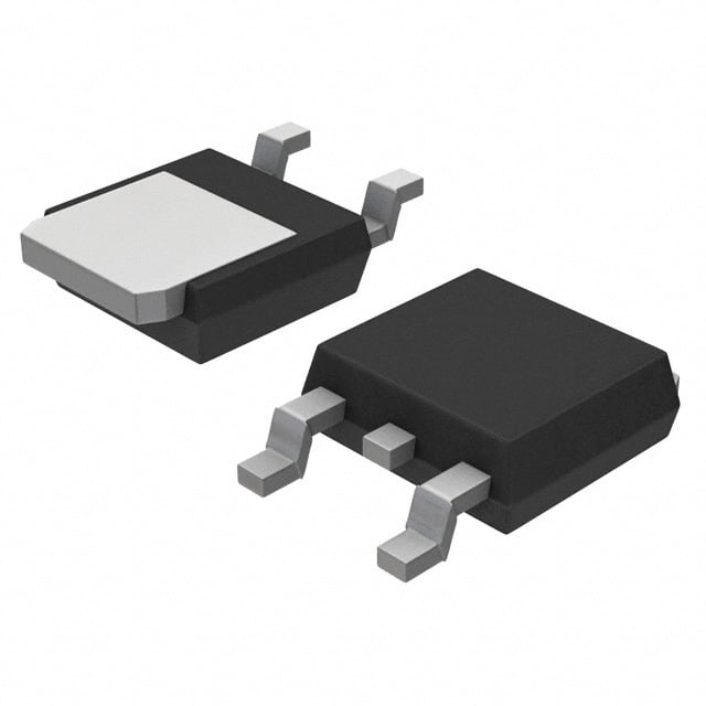
| 产品图片 |
|
| 产品型号 | NCV8664DT50RKG |
| rohs | 无铅 / 符合限制有害物质指令(RoHS)规范要求 |
| 产品系列 | - |
| 供应商器件封装 | DPAK-3 |
| 其它名称 | NCV8664DT50RKG-ND |
| 包装 | 带卷 (TR) |
| 安装类型 | 表面贴装 |
| 封装/外壳 | TO-252-3,DPak(2 引线+接片),SC-63 |
| 工作温度 | -40°C ~ 150°C |
| 标准包装 | 2,500 |
| 电压-跌落(典型值) | 0.315V @ 150mA |
| 电压-输入 | 最高 45 V |
| 电压-输出 | 5V |
| 电流-输出 | 150mA |
| 电流-限制(最小值) | 150mA |
| 稳压器拓扑 | 正,固定式 |
| 稳压器数 | 1 |


- 商务部:美国ITC正式对集成电路等产品启动337调查
- 曝三星4nm工艺存在良率问题 高通将骁龙8 Gen1或转产台积电
- 太阳诱电将投资9.5亿元在常州建新厂生产MLCC 预计2023年完工
- 英特尔发布欧洲新工厂建设计划 深化IDM 2.0 战略
- 台积电先进制程称霸业界 有大客户加持明年业绩稳了
- 达到5530亿美元!SIA预计今年全球半导体销售额将创下新高
- 英特尔拟将自动驾驶子公司Mobileye上市 估值或超500亿美元
- 三星加码芯片和SET,合并消费电子和移动部门,撤换高东真等 CEO
- 三星电子宣布重大人事变动 还合并消费电子和移动部门
- 海关总署:前11个月进口集成电路产品价值2.52万亿元 增长14.8%


PDF Datasheet 数据手册内容提取
NCV8664 Linear Regulator, Low Dropout, Very Low I q The NCV8664 is a precision 3.3 V and 5.0 V fixed output, low dropout integrated voltage regulator with an output current capability of 150 mA. Careful management of light load current consumption, combined with a low leakage process, achieve a www.onsemi.com typical quiescent current of 22 (cid:2)A. NCV8664 is pin and functionally compatible with NCV4264 and MARKING NCV4264−2, and it could replace these parts when very low DIAGRAMS quiescent current is required. The output voltage is accurate within ±2.0%, and maximum TAB SOT−223 AYW dropout voltage is 600 mV at full rated load current. ST SUFFIX V664x(cid:2) It is internally protected against input supply reversal, output 12 CASE 318E (cid:2) 3 overcurrent faults, and excess die temperature. No external 1 components are required to enable these features. F•ea3t.3u rVe,s 5.0 V Fixed Output 4 DTD SPUAFKFIX V664xxG • ±2.0% Output Accuracy, Over Full Temperature Range 1 2 CASE 369C ALYWW • 30 (cid:2)A Maximum Quiescent Current at I = 100 (cid:2)A 3 OUT 1 • 600 mV Maximum Dropout Voltage at 150 mA Load Current • 8 Wide Input Voltage Operating Range of 4.5 V to 45 V • Internal Fault Protection 8 SOIC−8 Fused V664x ALYWX CASE 751 ♦ −42 V Reverse Voltage 1 (cid:2) ♦ Short Circuit/Overcurrent 1 ♦ Thermal Overload • xx = Voltage Rating DPAK NCV Prefix for Automotive and Other Applications Requiring (50 = 5.0 V Version) Unique Site and Control Change Requirements; AEC−Q100 (33 = 3.3 V Version) Qualified and PPAP Capable x = Voltage Rating SOT223 • EMC Compliant (5 = 5.0 V Version) • (3 = 3.3 V Version) These are Pb−Free Devices A = Assembly Location L = Wafer Lot Y = Year W, WW = Work Week (cid:2) or G = Pb−Free Package (Note: Microdot may be in either location) PIN CONNECTIONS (SOT−223/DPAK) (SOIC−8 Fused) PIN FUNCTION PIN FUNCTION 1 VIN 1 NC 2,TAB GND 2, VIN 3 VOUT 3 GND 4. VOUT 5−8. NC ORDERING INFORMATION See detailed ordering and shipping information in the package dimensions section on page 11 of this data sheet. © Semiconductor Components Industries, LLC, 2010 1 Publication Order Number: November, 2018 − Rev. 19 NCV8664/D
NCV8664 IN OUT Bias Current Generators 1.3 V + Reference Error Amp - Thermal Shutdown GND Figure 1. Block Diagram PIN FUNCTION DESCRIPTION Pin No. DPAK/SOT−223 SOIC−8 Symbol Function 1 2 VIN Unregulated input voltage; 4.5 V to 45 V. 2 3 GND Ground; substrate. 3 4 VOUT Regulated output voltage; collector of the internal PNP pass transistor. TAB − GND Ground; substrate and best thermal connection to the die. − 1, 5−8 NC No Connection. OPERATING RANGE Pin Symbol, Parameter Symbol Min Max Unit VIN, DC Input Operating Voltage VIN 4.5 +45 V Junction Temperature Operating Range TJ −40 +150 °C MAXIMUM RATINGS Rating Symbol Min Max Unit VIN, DC Voltage VIN −42 +45 V VOUT, DC Voltage VOUT −0.3 +18 V Storage Temperature Tstg −55 +150 °C ESD Capability, Human Body Model (Note 1) VESDHB 4000 − V ESD Capability, Machine Model (Note 1) VESDMIM 200 − V Stresses exceeding those listed in the Maximum Ratings table may damage the device. If any of these limits are exceeded, device functionality should not be assumed, damage may occur and reliability may be affected. 1. This device series incorporates ESD protection and is tested by the following methods: ESD HBM tested per AEC−Q100−002 (EIA/JESD22−A 114C) ESD MM tested per AEC−Q100−003 (EIA/JESD22−A 115C) THERMAL RESISTANCE Parameter Symbol Condition Min Max Unit Junction−to−Ambient DPAK R(cid:3)JA − 101 (Note 2) °C/W SOT−223 − 99 (Note 2) SOIC−8 Fused − 145 Junction−to−Case DPAK R(cid:3)JC − 9.0 °C/W SOT−223 − 17 SOIC−8 Fused − − 2. 1 oz., 100 mm2 copper area. www.onsemi.com 2
NCV8664 LEAD SOLDERING TEMPERATURE AND MSL Rating Symbol Min Max Unit Lead Temperature Soldering Tsld °C Reflow (SMD Styles Only), Lead Free (Note 3) − 265 pk Moisture Sensitivity Level SOT223 MSL 3 − − DPAK 2 − SOIC−8 Fused 1 − 3. Lead Free, 60 sec – 150 sec above 217°C, 40 sec max at peak. ELECTRICAL CHARACTERISTICS (VIN = 13.5 V, Tj = −40°C to +150°C, unless otherwise noted.) Characteristic Symbol Test Conditions Min Typ Max Unit Output Voltage VOUT 0.1 mA (cid:2) IOUT (cid:2) 150 mA (Note 4) 4.900 5.000 5.100 V 5.0 V Version 6.0 V (cid:2) VIN (cid:2) 28 V Output Voltage VOUT 0 mA (cid:2) IOUT (cid:2) 150 mA 4.900 5.000 5.100 V 5.0 V Version 5.5 V (cid:2) VIN (cid:2) 28 V −40°C (cid:2) TJ (cid:2) 125°C Output Voltage VOUT 0.1 mA (cid:2) IOUT (cid:2) 150 mA (Note 4) 3.234 3.300 3.366 V 3.3 V Version 4.5 V (cid:2) VIN (cid:2) 28 V Line Regulation (cid:4)VOUT vs. VIN IOUT = 5.0 mA −25 5.0 +25 mV 5.0 V Version 6.0 V (cid:2) VIN (cid:2) 28 V Line Regulation (cid:4)VOUT vs. VIN IOUT = 5.0 mA −25 5.0 +25 mV 3.3 V Version 4.5 V (cid:2) VIN (cid:2) 28 V Load Regulation (cid:4)VOUT vs. IOUT 1.0 mA (cid:2) IOUT (cid:2) 150 mA −35 5.0 +35 mV (Note 4) Dropout Voltage VIN−VOUT IQ = 100 mA (Notes 4 & 5) − 265 500 mV 5.0 V Version IQ = 150 mA (Notes 4 & 5) − 315 600 Dropout Voltage VIN−VOUT IQ = 100 mA (Notes 4 & 7) − − 1.266 V 3.3 V Version IQ = 150 mA (Notes 4 & 7) − − 1.266 Quiescent Current Iq IOUT = 100 (cid:2)A (cid:2)A TJ = 25°C − 21 29 TJ = −40°C to +85°C − 22 30 Active Ground Current IG(ON) IOUT = 50 mA (Note 4) − 1.3 3 mA IOUT = 150 mA (Note 4) − 8.0 15 Power Supply Rejection PSRR VRIPPLE = 0.5 VP−P, F = 100 Hz − 67 − dB Output Capacitor for Stability COUT IOUT = 0.1 mA to 150 mA 10 − − (cid:2)F 5.0 V Version ESR (Note 4) − − 9.0 (cid:5) Output Capacitor for Stability COUT IOUT = 0.1 mA to 150 mA 22 − − (cid:2)F 3.3 V Version ESR (Note 4) − − 18 (cid:5) PROTECTION Current Limit IOUT(LIM) VOUT = 4.5 V (5.0 V Version) (Note 4) 150 − 500 mA VOUT = 3.0 V (3.3 V Version) (Note 4) 150 − 500 Short Circuit Current Limit IOUT(SC) VOUT = 0 V (Note 4) 100 − 500 mA Thermal Shutdown Threshold TTSD (Note 6) 150 − 200 °C Product parametric performance is indicated in the Electrical Characteristics for the listed test conditions, unless otherwise noted. Product performance may not be indicated by the Electrical Characteristics if operated under different conditions. 4. Use pulse loading to limit power dissipation. 5. Dropout voltage = (VIN – VOUT), measured when the output voltage has dropped 100 mV relative to the nominal value obtained with VIN = 13.5 V. 6. Not tested in production. Limits are guaranteed by design. 7. VDO = VIN − VOUT. For output voltage set to < 4.5 V, VDO will be constrained by the minimum input voltage. www.onsemi.com 3
NCV8664 4.5−45 V II Vin 1 8664 3 Vout IQ Output Input 1.0C (cid:2)IFN 100 nF 2 C10O (cid:2)UFT, 5.0 V Version RL 22 (cid:2)F, 3.3 V Version GND Figure 2. Measurement Circuit 4.5−45 V Vin 1 8664 3 Vout Output Input CIN COUT 100 nF 2 10 (cid:2)F, 5.0 V Version 22 (cid:2)F, 3.3 V Version GND Figure 3. Applications Circuit www.onsemi.com 4
NCV8664 Typical Curves 1000 6.0 Maximum ESR Cout = 10, 22 (cid:2)F 5.0 100 V) E ( 4.0 G (cid:5)) 10 TA R ( OL 3.0 ES 1.0 T V U P 2.0 T U O 0.1 1.0 Stable Region Vin = 13.5 V 0.01 0 0 20 40 60 80 100 120 140 160 180 0 1.0 2.0 3.0 4.0 5.0 6.0 7.0 8.0 LOAD CURRENT (mA) INPUT VOLTAGE (V) Figure 4. ESR Characterization, 5.0 V Version Figure 5. Output Voltage vs. Input Voltage, 5.0 V Version 9.0 0.40 125°C 125°C A) 8.0 Vin = 13.5 V 25°C A) 0.35 Vin = 13.5 V 25°C m 7.0 m T ( −40°C T ( 0.30 −40°C N 6.0 N E E 0.25 R R R 5.0 R U U C C 0.20 T 4.0 T N N CE 3.0 CE 0.15 S S UIE 2.0 UIE 0.10 Q Q 1.0 0.05 0 0 0 50 100 150 200 0 5.0 10 15 20 OUTPUT CURRENT (mA) OUTPUT CURRENT (mA) Figure 6. Current Consumption vs. Output Figure 7. Current Consumption vs. Output Load, 5.0 V Version Load (Low Load), 5.0 V Version 45 12 A) 40 IVouint == 11030.5 (cid:2) VA A) 10 Vin = 13.5 V (cid:2)T ( 35 T (m Iout = 150 mA EN 30 EN 8.0 R R R 25 R U U C C 6.0 T 20 T CEN 15 CEN 4.0 Iout = 100 mA S S UIE 10 UIE Q Q 2.0 5.0 0 0 −50 0 50 100 150 −50 0 50 100 150 TEMPERATURE (°C) TEMPERATURE (°C) Figure 8. Quiescent Current vs. Temperature, Figure 9. Quiescent Current vs. Temperature, 5.0 V Version 5.0 V Version www.onsemi.com 5
NCV8664 Typical Curves 0.45 18 0.40 125°C A) 16 m 0.35 N ( 14 V) 0.30 25°C PTIO 12 UT ( 0.25 −40°C UM 10 O S OP 0.20 ON 8.0 R C D 0.15 T 6.0 N 0.10 RE 4.0 RL = 50 (cid:5) R 0.05 CU 2.0 RL = 100 (cid:5) 0 0 0 50 100 150 200 0 10 20 30 40 50 OUTPUT LOAD (mA) INPUT VOLTAGE (V) Figure 10. Dropout Voltage vs. Output Load, Figure 11. Current Consumption vs. Input 5.0 V Version Voltage, 5.0 V Version 160 5.10 5.08 140 Vin = 13.5 V mA) 120 V) 5.06 Load = 10 mA T ( E ( 5.04 EN 100 AG 5.02 R TA = 25°C LT T CUR 6800 TA = 125°C UT VO 45..9080 U P P T 4.96 T U U 40 O O 4.94 20 4.92 0 4.90 0 10 20 30 40 50 −50 0 50 100 150 INPUT VOLTAGE (V) TEMPERATURE (°C) Figure 12. Output Current vs. Input Voltage, Figure 13. Output Voltage vs. Temperature, 5.0 V Version 5.0 V Version 400 350 A) m 300 T ( N 250 E R R 200 U C T 150 U P UT 100 Vin = 13.5 V O 50 0 −50 0 50 100 150 TEMPERATURE (°C) Figure 14. Current Limit vs. Temperature, 5.0 V Version www.onsemi.com 6
NCV8664 Typical Curves 100 3.5 90 3.0 80 V) 70 E ( 2.5 G (cid:5)) 60 TA 2.0 R ( 50 OL ES 40 UT V 1.5 P 30 UT 1.0 O 1200 VCionu =t > 1 32.25 (cid:2)VF 0.5 Iout = 5 mA 0 0 0 25 50 75 100 125 150 0 10 20 30 40 OUTPUT LOAD (mA) INPUT VOLTAGE (V) Figure 15. ESR Stability, 3.3 V Version Figure 16. Output Voltage vs. Input Voltage, 3.3 V Version 9.0 0.50 125°C A) 8.0 25°C A) 0.45 125°C m 7.0 −40°C m 0.40 25°C NT ( 6.0 NT ( 0.35 −40°C E E R R 0.30 R 5.0 R U U C C 0.25 T 4.0 T N N 0.20 CE 3.0 CE S S 0.15 UIE 2.0 UIE 0.10 Q Q 1.0 Vin = 13.5 V 0.05 Vin = 13.5 V 0 0 0 50 100 150 200 0 5 10 15 20 25 OUTPUT LOAD (mA) OUTPUT LOAD (mA) Figure 17. Current Consumption vs. Output Figure 18. Current Consumption vs. Output Load, 3.3 V Version Load (Low Load), 3.3 V Version 45 10 40 9 A) A) Iout = 150 mA (cid:2) 35 (cid:2) 8 T ( T ( N N 7 E 30 E R R 6 R 25 R U U T C 20 T C 5 Iout = 100 mA N N 4 E E C 15 C S S 3 E E UI 10 UI 2 Q Vin = 13.5 V Q 5 Iout = 100 (cid:2)A 1 Vin = 13.5 V 0 0 −40 10 60 110 150 −40 10 60 110 150 TEMPERATURE (°C) TEMPERATURE (°C) Figure 19. Quiescent Current vs. Temperature, Figure 20. Quiescent Current vs. Temperature, 3.3 V Version 3.3 V Version www.onsemi.com 7
NCV8664 Typical Curves 0.45 7 0.40 125°C A) 6 m E (V) 0.35 ON ( 5 G 0.30 25°C TI A P OLT 0.25 −40°C UM 4 V S T 0.20 ON 3 OPOU 0.15 NT C 2 RL = 50 (cid:5) DR 0.10 RE R 0.05 CU 1 RL = 100 (cid:5) 0 0 0 50 100 150 200 0 10 20 30 40 50 OUTPUT LOAD (mA) INPUT VOLTAGE (V) Figure 21. Dropout Voltage, 3.3 V Version Figure 22. Current Consumption vs. Input Voltage, 3.3 V Version 3.50 250 3.45 3.40 200 V) A) E ( 3.35 m G T ( TA 3.30 MI 150 VOL 3.25 T LI UTPUT 33..1250 URREN 100 O C 3.10 Vin = 14 V 50 3.05 Iout = 5 mA Vin = 13.5 V 3.00 0 −40 −20 0 20 40 60 80 100 120125 −40 10 60 110 150 TEMPERATURE (°C) TEMPERATURE (°C) Figure 23. Output Voltage vs. Temperature, Figure 24. Short Circuit Current Limit vs. 3.3 V Version Temperature, 3.3 V Version www.onsemi.com 8
NCV8664 Circuit Description Calculating Power Dissipation in a Single Output The NCV8664 is a precision trimmed 3.3 V and 5.0 V Linear Regulator fixed output regulator. Careful management of light load The maximum power dissipation for a single output consumption combined with a low leakage process results regulator (Figure 3) is: in a typical quiescent current of 22 (cid:2)A. The device has PD(max)(cid:5)[VIN(max)(cid:6)VOUT(min)](cid:4) current capability of 150 mA, with 600 mV of dropout IQ(max)(cid:3)VI(max)(cid:4)Iq (eq. 1) voltage at full rated load current. The regulation is provided by a PNP pass transistor controlled by an error amplifier Where: with a bandgap reference. The regulator is protected by VIN(max) is the maximum input voltage, both current limit and short circuit protection. Thermal VOUT(min) is the minimum output voltage, shutdown occurs above 150°C to protect the IC during IQ(max) is the maximum output current for the overloads and extreme ambient temperatures. application, and Iq is the quiescent current the regulator consumes at I . Q(max) Regulator Once the value of P is known, the maximum D(Max) The error amplifier compares the reference voltage to a permissible value of R(cid:3)JA can be calculated: saa PmNpPle s oerfi ethse p oasust pturat nvsoislttoagr eb y(V ao butu) fafenrd. Tdrhiev erse ftehree nbcaes ei so af P(cid:3)JA(cid:5)150oC(cid:6)TA (eq. 2) PD bandgap design to give it a temperature−stable output. Saturation control of the PNP is a function of the load The value of R(cid:3)JA can then be compared with those in the package section of the data sheet. Those packages with current and input voltage. Over saturation of the output power device is prevented, and quiescent current in the R(cid:3)JA’s less than the calculated value in Equation 2 will keep the die temperature below 150°C. In some cases, none of ground pin is minimized. The NCV8664 is equipped with the packages will be sufficient to dissipate the heat foldback current protection. This protection is designed to generated by the IC, and an external heat sink will be reduce the current limit during an overcurrent situation. required. The current flow and voltages are shown in the Regulator Stability Considerations Measurement Circuit Diagram. The input capacitor C in Figure 2 is necessary for IN Heat Sinks compensating input line reactance. Possible oscillations For proper heat sinking of the SOIC−8 Lead device, caused by input inductance and input capacitance can be connect pins 5 − 8 to the heat sink. damped by using a resistor of approximately 1 (cid:5) in series A heat sink effectively increases the surface area of the with C . The output or compensation capacitor, C IN OUT package to improve the flow of heat away from the IC and helps determine three main characteristics of a linear into the surrounding air. Each material in the heat flow path regulator: startup delay, load transient response and loop between the IC and the outside environment will have a stability. The capacitor value and type should be based on thermal resistance. Like series electrical resistances, these cost, availability, size and temperature constraints. Tantalum, aluminum electrolytic, film, or ceramic resistances are summed to determine the value of R(cid:3)JA: capacitors are all acceptable solutions, however, attention R(cid:3)JA(cid:5)R(cid:3)JC(cid:3)R(cid:3)CS(cid:3)R(cid:3)SA (eq. 3) must be paid to ESR constraints. The aluminum Where: electrolytic capacitor is the least expensive solution, but, if the circuit operates at low temperatures (−25°C to −40°C), R(cid:3)JC = the junction−to−case thermal resistance, R(cid:3)CS = the case−to−heat sink thermal resistance, and both the value and ESR of the capacitor will vary R(cid:3)SA = the heat sink−to−ambient thermal resistance. considerably. The capacitor manufacturer’s data sheet R(cid:3)JA appears in the package section of the data sheet. usually provides this information. The value for the output Like R(cid:3)JA, it too is a function of package type. R(cid:3)CS and capacitor C shown in Figure 2 should work for most OUT R(cid:3)SA are functions of the package type, heat sink and the applications; however, it is not necessarily the optimized interface between them. These values appear in data sheets solution. Stability is guaranteed at values C ≥ 10 (cid:2)F and OUT of heat sink manufacturers. Thermal, mounting, and heat ESR ≤ 9(cid:5) for 5.0 V version, and C ≥ 22 (cid:2)F and ESR OUT sinking are discussed in the ON Semiconductor application ≤ 18(cid:5) for 3.3V version, within the operating temperature note AN1040/D, available on the ON Semiconductor range. Actual limits are shown in a graph in the Typical Website. Performance Characteristics section. www.onsemi.com 9
NCV8664 EMC−Characteristics: Conducted Susceptibility Direct Power Injection: 33 dBm forward power CW All EMC−Characteristics are based on limited samples Acceptance Criteria: Amplitude Dev. max 2% of Output and not part of production testing, according to Voltage 47A/658/CD IEC62132−4 (Direct Power Injection) Test Conditions Supply Voltage V = 12 V IN Temperature TA = 23°C ±5°C Load RL = 35 (cid:5) U1 NCV8664 X1 1 VIN VOUT 3 X3 VIN_HF VOUT_HF F3 GND F1 FERRITE C2 + C1 2 C3 + FERRITE 47 nF 10 nF C4 X2 10 (cid:2)F 10 (cid:2)F X4 VIN_MON VOUT_MON F2 FERRITE X5 X6 GND_HF GND_MON Figure 25. Test Circuit 40 40 VIN−pin pass 33 dBm VOUT−pin pass 33 dBm 30 30 m) Bm) B d (dN 20 (UT 20 VI O V 10 10 0 0 1 10 100 1000 1 10 100 1000 FREQUENCY (MHz) FREQUENCY (MHz) Figure 26. Typical V −pin Susceptibility Figure 27. Typical V −pin Susceptibility IN OUT www.onsemi.com 10
NCV8664 160 140 120 SOIC−8 Fused W) 100 °C/ 80 SOT223 A ( (cid:3)J 60 DPAK 40 20 0 0 100 200 300 400 500 600 700 COPPER AREA (mm2) Figure 28. (cid:2)JA vs. Copper Spreader Area 1000 100 SOT223 SOIC−8 Fused 10 DPAK W) C/ 1 ° R(t) ( 0.1 0.01 0.001 0.000001 0.00001 0.0001 0.001 0.01 0.1 1 10 100 1000 PULSE TIME (sec) Figure 29. Single−Pulse Heating Curves ORDERING INFORMATION Device* Marking Package Shipping† NCV8664D50R2G V6645 SOIC−8 Fused 2500 / Tape & Reel (Pb−Free) NCV8664D50G V6645 SOIC−8 Fused 98 Units / Rail (Pb−Free) NCV8664DT50RKG V66450G DPAK 2500 / Tape & Reel (Pb−Free) NCV8664DT33RKG V66433G DPAK 2500 / Tape & Reel (Pb−Free) NCV8664ST50T3G V6645 SOT−223 4000 / Tape & Reel (Pb−Free) NCV8664ST33T3G V6643 SOT−223 4000 / Tape & Reel (Pb−Free) †For information on tape and reel specifications, including part orientation and tape sizes, please refer to our Tape and Reel Packaging Specification Brochure, BRD8011/D. *NCV Prefix for Automotive and Other Applications Requiring Unique Site and Control Change Requirements; AEC−Q100 Qualified and PPAP Capable. www.onsemi.com 11
MECHANICAL CASE OUTLINE PACKAGE DIMENSIONS SOT−223 (TO−261) CASE 318E−04 ISSUE R SCALE 1:1 DATE 02 OCT 2018 (cid:2) (cid:2) Electronic versions are uncontrolled except when accessed directly from the Document Repository. DOCUMENT NUMBER: 98ASB42680B Printed versions are uncontrolled except when stamped “CONTROLLED COPY” in red. DESCRIPTION: SOT−223 (TO−261) PAGE 1 OF 2 ON Semiconductor and are trademarks of Semiconductor Components Industries, LLC dba ON Semiconductor or its subsidiaries in the United States and/or other countries. ON Semiconductor reserves the right to make changes without further notice to any products herein. ON Semiconductor makes no warranty, representation or guarantee regarding the suitability of its products for any particular purpose, nor does ON Semiconductor assume any liability arising out of the application or use of any product or circuit, and specifically disclaims any and all liability, including without limitation special, consequential or incidental damages. ON Semiconductor does not convey any license under its patent rights nor the rights of others. © Semiconductor Components Industries, LLC, 2018 www.onsemi.com
SOT−223 (TO−261) CASE 318E−04 ISSUE R DATE 02 OCT 2018 STYLE 1: STYLE 2: STYLE 3: STYLE 4: STYLE 5: PIN 1.BASE PIN 1.ANODE PIN 1.GATE PIN 1.SOURCE PIN 1.DRAIN 2.COLLECTOR 2.CATHODE 2.DRAIN 2.DRAIN 2.GATE 3.EMITTER 3.NC 3.SOURCE 3.GATE 3.SOURCE 4.COLLECTOR 4.CATHODE 4.DRAIN 4.DRAIN 4.GATE STYLE 6: STYLE 7: STYLE 8: STYLE 9: STYLE 10: PIN 1.RETURN PIN 1.ANODE 1 CANCELLED PIN 1.INPUT PIN 1.CATHODE 2.INPUT 2.CATHODE 2.GROUND 2.ANODE 3.OUTPUT 3.ANODE 2 3.LOGIC 3.GATE 4.INPUT 4.CATHODE 4.GROUND 4.ANODE STYLE 11: STYLE 12: STYLE 13: PIN 1.MT 1 PIN 1.INPUT PIN 1.GATE 2.MT 2 2.OUTPUT 2.COLLECTOR 3.GATE 3.NC 3.EMITTER 4.MT 2 4.OUTPUT 4.COLLECTOR GENERIC MARKING DIAGRAM* AYW XXXXX(cid:2) (cid:2) 1 A = Assembly Location Y = Year W = Work Week XXXXX = Specific Device Code (cid:2) = Pb−Free Package (Note: Microdot may be in either location) *This information is generic. Please refer to device data sheet for actual part marking. Pb−Free indicator, “G” or microdot “(cid:2)”, may or may not be present. Some products may not follow the Generic Marking. Electronic versions are uncontrolled except when accessed directly from the Document Repository. DOCUMENT NUMBER: 98ASB42680B Printed versions are uncontrolled except when stamped “CONTROLLED COPY” in red. DESCRIPTION: SOT−223 (TO−261) PAGE 2 OF 2 ON Semiconductor and are trademarks of Semiconductor Components Industries, LLC dba ON Semiconductor or its subsidiaries in the United States and/or other countries. ON Semiconductor reserves the right to make changes without further notice to any products herein. ON Semiconductor makes no warranty, representation or guarantee regarding the suitability of its products for any particular purpose, nor does ON Semiconductor assume any liability arising out of the application or use of any product or circuit, and specifically disclaims any and all liability, including without limitation special, consequential or incidental damages. ON Semiconductor does not convey any license under its patent rights nor the rights of others. © Semiconductor Components Industries, LLC, 2018 www.onsemi.com
MECHANICAL CASE OUTLINE PACKAGE DIMENSIONS 4 DPAK (SINGLE GAUGE) CASE 369C ISSUE F 1 2 DATE 21 JUL 2015 3 SCALE 1:1 NOTES: A 1.DIMENSIONING AND TOLERANCING PER ASME Y14.5M, 1994. E C 2.CONTROLLING DIMENSION: INCHES. A 3.THERMAL PAD CONTOUR OPTIONAL WITHIN DI- b3 B MENSIONS b3, L3 and Z. c2 4.DIMENSIONS D AND E DO NOT INCLUDE MOLD FLASH, PROTRUSIONS, OR BURRS. MOLD FLASH, PROTRUSIONS, OR GATE BURRS SHALL 4 NOT EXCEED 0.006 INCHES PER SIDE. L3 Z 5.DIMENSIONS D AND E ARE DETERMINED AT THE D DETAIL A H 6.DOAUTTUEMRSM OA SATN EDX BT RAERME EDSE OTEFR TMHIEN EPDLA ASTT DICA TBUOMDY. 1 2 3 PLANE H. 7.OPTIONAL MOLD FEATURE. L4 INCHES MILLIMETERS NOTE 7 b2 c BOTTOM VIEW DIM MIN MAX MIN MAX A 0.086 0.094 2.18 2.38 e SIDE VIEW A1 0.000 0.005 0.00 0.13 b b 0.025 0.035 0.63 0.89 0.005 (0.13) M C b2 0.028 0.045 0.72 1.14 TOP VIEW b3 0.180 0.215 4.57 5.46 c 0.018 0.024 0.46 0.61 c2 0.018 0.024 0.46 0.61 H Z Z D 0.235 0.245 5.97 6.22 E 0.250 0.265 6.35 6.73 e 0.090 BSC 2.29 BSC L2 GPLAAUNGEE C SPELAATNIENG H 0.370 0.410 9.40 10.41 L 0.055 0.070 1.40 1.78 L1 0.114 REF 2.90 REF L2 0.020 BSC 0.51 BSC L A1 BOTTOM VIEW L3 0.035 0.050 0.89 1.27 L1 ALTERNATE L4 −−− 0.040 −−− 1.01 CONSTRUCTIONS Z 0.155 −−− 3.93 −−− DETAIL A ROTATED 90(cid:2) CW GENERIC MARKING DIAGRAM* STYLE 1: STYLE 2: STYLE 3: STYLE 4: STYLE 5: PIN 1.BASE PIN 1.GATE PIN 1.ANODE PIN 1.CATHODE PIN 1.GATE 2.COLLECTOR 2.DRAIN 2.CATHODE 2.ANODE 2.ANODE 3.EMITTER 3.SOURCE 3.ANODE 3.GATE 3.CATHODE 4.COLLECTOR 4.DRAIN 4.CATHODE 4.ANODE 4.ANODE XXXXXXG AYWW ALYWW XXX STYLE 6: STYLE 7: STYLE 8: STYLE 9: STYLE 10: XXXXXG PIN 1.MT1 PIN 1.GATE PIN 1.N/C PIN 1.ANODE PIN 1.CATHODE 2.MT2 2.COLLECTOR 2.CATHODE 2.CATHODE 2.ANODE 3.GATE 3.EMITTER 3.ANODE 3.RESISTOR ADJUST 3.CATHODE 4.MT2 4.COLLECTOR 4.CATHODE 4.CATHODE 4.ANODE IC Discrete SOLDERING FOOTPRINT* XXXXXX = Device Code A = Assembly Location 6.20 3.00 L = Wafer Lot 0.244 0.118 2.58 Y = Year 0.102 WW = Work Week G = Pb−Free Package *This information is generic. Please refer 5.80 1.60 6.17 to device data sheet for actual part 0.228 0.063 0.243 marking. (cid:2) (cid:3) mm SCALE 3:1 inches *For additional information on our Pb−Free strategy and soldering details, please download the ON Semiconductor Soldering and Mounting Techniques Reference Manual, SOLDERRM/D. DOCUMENT NUMBER: 98AON10527D Electronic versions are uncontrolled except when accessed directly from the Document Repository. Printed STATUS: ON SEMICONDUCTOR STANDARD versions are uncontrolled except when stamped “CONTROLLED COPY” in red. NEW STANDARD: REF TO JEDEC TO−252 © Semiconductor Components Industries, LLC, 2002 http://onsemi.com Case Outline Number: October, D20E0S2C −R RIePvT. I0ON: DPAK SINGLE GAUGE SURFA1CE MOUNT PAGE 1 OFX 2XX
DOCUMENT NUMBER: 98AON10527D PAGE 2 OF 2 ISSUE REVISION DATE O RELEASED FOR PRODUCTION. REQ. BY L. GAN 24 SEP 2001 A ADDED STYLE 8. REQ. BY S. ALLEN. 06 AUG 2008 B ADDED STYLE 9. REQ. BY D. WARNER. 16 JAN 2009 C ADDED STYLE 10. REQ. BY S. ALLEN. 09 JUN 2009 D RELABELED DRAWING TO JEDEC STANDARDS. ADDED SIDE VIEW DETAIL A. 29 JUN 2010 CORRECTED MARKING INFORMATION. REQ. BY D. TRUHITTE. E ADDED ALTERNATE CONSTRUCTION BOTTOM VIEW. MODIFIED DIMENSIONS 06 FEB 2014 b2 AND L1. CORRECTED MARKING DIAGRAM FOR DISCRETE. REQ. BY I. CAM- BALIZA. F ADDED SECOND ALTERNATE CONSTRUCTION BOTTOM VIEW. REQ. BY K. 21 JUL 2015 MUSTAFA. ON Semiconductor and are registered trademarks of Semiconductor Components Industries, LLC (SCILLC). SCILLC reserves the right to make changes without further notice to any products herein. SCILLC makes no warranty, representation or guarantee regarding the suitability of its products for any particular purpose, nor does SCILLC assume any liability arising out of the application or use of any product or circuit, and specifically disclaims any and all liability, including without limitation special, consequential or incidental damages. “Typical” parameters which may be provided in SCILLC data sheets and/or specifications can and do vary in different applications and actual performance may vary over time. All operating parameters, including “Typicals” must be validated for each customer application by customer’s technical experts. SCILLC does not convey any license under its patent rights nor the rights of others. SCILLC products are not designed, intended, or authorized for use as components in systems intended for surgical implant into the body, or other applications intended to support or sustain life, or for any other application in which the failure of the SCILLC product could create a situation where personal injury or death may occur. Should Buyer purchase or use SCILLC products for any such unintended or unauthorized application, Buyer shall indemnify and hold SCILLC and its officers, employees, subsidiaries, affiliates, and distributors harmless against all claims, costs, damages, and expenses, and reasonable attorney fees arising out of, directly or indirectly, any claim of personal injury or death associated with such unintended or unauthorized use, even if such claim alleges that SCILLC was negligent regarding the design or manufacture of the part. SCILLC is an Equal Opportunity/Affirmative Action Employer. This literature is subject to all applicable copyright laws and is not for resale in any manner. © Semiconductor Components Industries, LLC, 2015 Case Outline Number: July, 2015 − Rev. F 369C
MECHANICAL CASE OUTLINE PACKAGE DIMENSIONS SOIC−8 NB CASE 751−07 8 ISSUE AK 1 DATE 16 FEB 2011 SCALE 1:1 NOTES: −X− 1. DIMENSIONING AND TOLERANCING PER ANSI Y14.5M, 1982. A 2. CONTROLLING DIMENSION: MILLIMETER. 3. DIMENSION A AND B DO NOT INCLUDE MOLD PROTRUSION. 4. MAXIMUM MOLD PROTRUSION 0.15 (0.006) 8 5 PER SIDE. 5. DIMENSION D DOES NOT INCLUDE DAMBAR B S 0.25 (0.010) M Y M PROTRUSION. ALLOWABLE DAMBAR PROTRUSION SHALL BE 0.127 (0.005) TOTAL 1 IN EXCESS OF THE D DIMENSION AT −Y− 4 K 6. M75A1X−I0M1U TMH RMUA T7E51R−IA0L6 CAROEN DOIBTSIOONL.ETE. NEW STANDARD IS 751−07. G MILLIMETERS INCHES DIM MIN MAX MIN MAX A 4.80 5.00 0.189 0.197 C NX 45(cid:2) B 3.80 4.00 0.150 0.157 SEATING C 1.35 1.75 0.053 0.069 PLANE D 0.33 0.51 0.013 0.020 −Z− G 1.27 BSC 0.050 BSC H 0.10 0.25 0.004 0.010 0.10 (0.004) J 0.19 0.25 0.007 0.010 H D M J K 0.40 1.27 0.016 0.050 M 0 (cid:2) 8 (cid:2) 0 (cid:2) 8 (cid:2) N 0.25 0.50 0.010 0.020 0.25 (0.010)M Z Y S X S S 5.80 6.20 0.228 0.244 GENERIC MARKING DIAGRAM* SOLDERING FOOTPRINT* 8 8 8 8 XXXXX XXXXX XXXXXX XXXXXX 1.52 ALYWX ALY (cid:3)WX AYWW AY W(cid:3)W 0.060 1 1 1 1 IC IC Discrete Discrete (Pb−Free) (Pb−Free) 7.0 4.0 XXXXX = Specific Device Code XXXXXX= Specific Device Code 0.275 0.155 A = Assembly Location A = Assembly Location L = Wafer Lot Y = Year Y = Year WW = Work Week W = Work Week (cid:3) = Pb−Free Package (cid:3) = Pb−Free Package 0.6 1.270 *This information is generic. Please refer 0.024 0.050 to device data sheet for actual part marking. Pb−Free indicator, “G”, may (cid:2) (cid:3) mm or not be present. SCALE 6:1 inches *For additional information on our Pb−Free strategy and soldering details, please download the ON Semiconductor Soldering and Mounting Techniques Reference Manual, SOLDERRM/D. STYLES ON PAGE 2 DOCUMENT NUMBER: 98ASB42564B Electronic versions are uncontrolled except when accessed directly from the Document Repository. Printed STATUS: ON SEMICONDUCTOR STANDARD versions are uncontrolled except when stamped “CONTROLLED COPY” in red. NEW STANDARD: © Semiconductor Components Industries, LLC, 2002 http://onsemi.com Case Outline Number: October, D20E0S2C −R RIePvT. I0ON: SOIC−8, NB 1 PAGE 1 OFX 3XX
SOIC−8 NB CASE 751−07 ISSUE AK DATE 16 FEB 2011 STYLE 1: STYLE 2: STYLE 3: STYLE 4: PIN 1. EMITTER PIN 1. COLLECTOR, DIE, #1 PIN 1. DRAIN, DIE #1 PIN 1. ANODE 2. COLLECTOR 2. COLLECTOR, #1 2. DRAIN, #1 2. ANODE 3. COLLECTOR 3. COLLECTOR, #2 3. DRAIN, #2 3. ANODE 4. EMITTER 4. COLLECTOR, #2 4. DRAIN, #2 4. ANODE 5. EMITTER 5. BASE, #2 5. GATE, #2 5. ANODE 6. BASE 6. EMITTER, #2 6. SOURCE, #2 6. ANODE 7. BASE 7. BASE, #1 7. GATE, #1 7. ANODE 8. EMITTER 8. EMITTER, #1 8. SOURCE, #1 8. COMMON CATHODE STYLE 5: STYLE 6: STYLE 7: STYLE 8: PIN 1. DRAIN PIN 1. SOURCE PIN 1. INPUT PIN 1. COLLECTOR, DIE #1 2. DRAIN 2. DRAIN 2. EXTERNAL BYPASS 2. BASE, #1 3. DRAIN 3. DRAIN 3. THIRD STAGE SOURCE 3. BASE, #2 4. DRAIN 4. SOURCE 4. GROUND 4. COLLECTOR, #2 5. GATE 5. SOURCE 5. DRAIN 5. COLLECTOR, #2 6. GATE 6. GATE 6. GATE 3 6. EMITTER, #2 7. SOURCE 7. GATE 7. SECOND STAGE Vd 7. EMITTER, #1 8. SOURCE 8. SOURCE 8. FIRST STAGE Vd 8. COLLECTOR, #1 STYLE 9: STYLE 10: STYLE 11: STYLE 12: PIN 1. EMITTER, COMMON PIN 1. GROUND PIN 1. SOURCE 1 PIN 1. SOURCE 2. COLLECTOR, DIE #1 2. BIAS 1 2. GATE 1 2. SOURCE 3. COLLECTOR, DIE #2 3. OUTPUT 3. SOURCE 2 3. SOURCE 4. EMITTER, COMMON 4. GROUND 4. GATE 2 4. GATE 5. EMITTER, COMMON 5. GROUND 5. DRAIN 2 5. DRAIN 6. BASE, DIE #2 6. BIAS 2 6. DRAIN 2 6. DRAIN 7. BASE, DIE #1 7. INPUT 7. DRAIN 1 7. DRAIN 8. EMITTER, COMMON 8. GROUND 8. DRAIN 1 8. DRAIN STYLE 13: STYLE 14: STYLE 15: STYLE 16: PIN 1. N.C. PIN 1. N−SOURCE PIN 1. ANODE 1 PIN 1. EMITTER, DIE #1 2. SOURCE 2. N−GATE 2. ANODE 1 2. BASE, DIE #1 3. SOURCE 3. P−SOURCE 3. ANODE 1 3. EMITTER, DIE #2 4. GATE 4. P−GATE 4. ANODE 1 4. BASE, DIE #2 5. DRAIN 5. P−DRAIN 5. CATHODE, COMMON 5. COLLECTOR, DIE #2 6. DRAIN 6. P−DRAIN 6. CATHODE, COMMON 6. COLLECTOR, DIE #2 7. DRAIN 7. N−DRAIN 7. CATHODE, COMMON 7. COLLECTOR, DIE #1 8. DRAIN 8. N−DRAIN 8. CATHODE, COMMON 8. COLLECTOR, DIE #1 STYLE 17: STYLE 18: STYLE 19: STYLE 20: PIN 1. VCC PIN 1. ANODE PIN 1. SOURCE 1 PIN 1. SOURCE (N) 2. V2OUT 2. ANODE 2. GATE 1 2. GATE (N) 3. V1OUT 3. SOURCE 3. SOURCE 2 3. SOURCE (P) 4. TXE 4. GATE 4. GATE 2 4. GATE (P) 5. RXE 5. DRAIN 5. DRAIN 2 5. DRAIN 6. VEE 6. DRAIN 6. MIRROR 2 6. DRAIN 7. GND 7. CATHODE 7. DRAIN 1 7. DRAIN 8. ACC 8. CATHODE 8. MIRROR 1 8. DRAIN STYLE 21: STYLE 22: STYLE 23: STYLE 24: PIN 1. CATHODE 1 PIN 1. I/O LINE 1 PIN 1. LINE 1 IN PIN 1. BASE 2. CATHODE 2 2. COMMON CATHODE/VCC 2. COMMON ANODE/GND 2. EMITTER 3. CATHODE 3 3. COMMON CATHODE/VCC 3. COMMON ANODE/GND 3. COLLECTOR/ANODE 4. CATHODE 4 4. I/O LINE 3 4. LINE 2 IN 4. COLLECTOR/ANODE 5. CATHODE 5 5. COMMON ANODE/GND 5. LINE 2 OUT 5. CATHODE 6. COMMON ANODE 6. I/O LINE 4 6. COMMON ANODE/GND 6. CATHODE 7. COMMON ANODE 7. I/O LINE 5 7. COMMON ANODE/GND 7. COLLECTOR/ANODE 8. CATHODE 6 8. COMMON ANODE/GND 8. LINE 1 OUT 8. COLLECTOR/ANODE STYLE 25: STYLE 26: STYLE 27: STYLE 28: PIN 1. VIN PIN 1. GND PIN 1. ILIMIT PIN 1. SW_TO_GND 2. N/C 2. dv/dt 2. OVLO 2. DASIC_OFF 3. REXT 3. ENABLE 3. UVLO 3. DASIC_SW_DET 4. GND 4. ILIMIT 4. INPUT+ 4. GND 5. IOUT 5. SOURCE 5. SOURCE 5. V_MON 6. IOUT 6. SOURCE 6. SOURCE 6. VBULK 7. IOUT 7. SOURCE 7. SOURCE 7. VBULK 8. IOUT 8. VCC 8. DRAIN 8. VIN STYLE 29: STYLE 30: PIN 1. BASE, DIE #1 PIN 1. DRAIN 1 2. EMITTER, #1 2. DRAIN 1 3. BASE, #2 3. GATE 2 4. EMITTER, #2 4. SOURCE 2 5. COLLECTOR, #2 5. SOURCE 1/DRAIN 2 6. COLLECTOR, #2 6. SOURCE 1/DRAIN 2 7. COLLECTOR, #1 7. SOURCE 1/DRAIN 2 8. COLLECTOR, #1 8. GATE 1 DOCUMENT NUMBER: 98ASB42564B Electronic versions are uncontrolled except when accessed directly from the Document Repository. Printed STATUS: ON SEMICONDUCTOR STANDARD versions are uncontrolled except when stamped “CONTROLLED COPY” in red. NEW STANDARD: © Semiconductor Components Industries, LLC, 2002 http://onsemi.com Case Outline Number: October, D20E0S2C −R RIePvT. I0ON: SOIC−8, NB 2 PAGE 2 OFX 3XX
DOCUMENT NUMBER: 98ASB42564B PAGE 3 OF 3 ISSUE REVISION DATE AB ADDED STYLE 25. REQ. BY S. CHANG. 15 MAR 2004 AC ADDED CORRECTED MARKING DIAGRAMS. REQ. BY S. FARRETTA. 13 AUG 2004 AD CORRECTED MARKING DIAGRAM FOR DISCRETE. REQ. BY S. FARRETTA. 18 NOV 2004 AE UPDATED SCALE ON FOOTPRINT. REQ. BY S. WEST. 31 JAN 2005 AF UPDATED MARKING DIAGRAMS. REQ. BY S. WEST. ADDED STYLE 26. REQ. BY 14 APR 2005 S. CHANG. AG ADDED STYLE 27. REQ. BY S. CHANG. 30 JUN 2005 AH ADDED STYLE 28. REQ. BY S. CHANG. 09 MAR 2006 AJ ADDED STYLE 29. REQ. BY D. HELZER. 19 SEP 2007 AK ADDED STYLE 30. REQ. BY I. CAMBALIZA. 16 FEB 2011 ON Semiconductor and are registered trademarks of Semiconductor Components Industries, LLC (SCILLC). SCILLC reserves the right to make changes without further notice to any products herein. SCILLC makes no warranty, representation or guarantee regarding the suitability of its products for any particular purpose, nor does SCILLC assume any liability arising out of the application or use of any product or circuit, and specifically disclaims any and all liability, including without limitation special, consequential or incidental damages. “Typical” parameters which may be provided in SCILLC data sheets and/or specifications can and do vary in different applications and actual performance may vary over time. All operating parameters, including “Typicals” must be validated for each customer application by customer’s technical experts. SCILLC does not convey any license under its patent rights nor the rights of others. SCILLC products are not designed, intended, or authorized for use as components in systems intended for surgical implant into the body, or other applications intended to support or sustain life, or for any other application in which the failure of the SCILLC product could create a situation where personal injury or death may occur. Should Buyer purchase or use SCILLC products for any such unintended or unauthorized application, Buyer shall indemnify and hold SCILLC and its officers, employees, subsidiaries, affiliates, and distributors harmless against all claims, costs, damages, and expenses, and reasonable attorney fees arising out of, directly or indirectly, any claim of personal injury or death associated with such unintended or unauthorized use, even if such claim alleges that SCILLC was negligent regarding the design or manufacture of the part. SCILLC is an Equal Opportunity/Affirmative Action Employer. This literature is subject to all applicable copyright laws and is not for resale in any manner. © Semiconductor Components Industries, LLC, 2011 Case Outline Number: February, 2011 − Rev. 07AK 751
ON Semiconductor and are trademarks of Semiconductor Components Industries, LLC dba ON Semiconductor or its subsidiaries in the United States and/or other countries. ON Semiconductor owns the rights to a number of patents, trademarks, copyrights, trade secrets, and other intellectual property. A listing of ON Semiconductor’s product/patent coverage may be accessed at www.onsemi.com/site/pdf/Patent−Marking.pdf. ON Semiconductor reserves the right to make changes without further notice to any products herein. ON Semiconductor makes no warranty, representation or guarantee regarding the suitability of its products for any particular purpose, nor does ON Semiconductor assume any liability arising out of the application or use of any product or circuit, and specifically disclaims any and all liability, including without limitation special, consequential or incidental damages. Buyer is responsible for its products and applications using ON Semiconductor products, including compliance with all laws, regulations and safety requirements or standards, regardless of any support or applications information provided by ON Semiconductor. “Typical” parameters which may be provided in ON Semiconductor data sheets and/or specifications can and do vary in different applications and actual performance may vary over time. All operating parameters, including “Typicals” must be validated for each customer application by customer’s technical experts. ON Semiconductor does not convey any license under its patent rights nor the rights of others. ON Semiconductor products are not designed, intended, or authorized for use as a critical component in life support systems or any FDA Class 3 medical devices or medical devices with a same or similar classification in a foreign jurisdiction or any devices intended for implantation in the human body. Should Buyer purchase or use ON Semiconductor products for any such unintended or unauthorized application, Buyer shall indemnify and hold ON Semiconductor and its officers, employees, subsidiaries, affiliates, and distributors harmless against all claims, costs, damages, and expenses, and reasonable attorney fees arising out of, directly or indirectly, any claim of personal injury or death associated with such unintended or unauthorized use, even if such claim alleges that ON Semiconductor was negligent regarding the design or manufacture of the part. ON Semiconductor is an Equal Opportunity/Affirmative Action Employer. This literature is subject to all applicable copyright laws and is not for resale in any manner. PUBLICATION ORDERING INFORMATION LITERATURE FULFILLMENT: N. American Technical Support: 800−282−9855 Toll Free ON Semiconductor Website: www.onsemi.com Literature Distribution Center for ON Semiconductor USA/Canada 19521 E. 32nd Pkwy, Aurora, Colorado 80011 USA Europe, Middle East and Africa Technical Support: Order Literature: http://www.onsemi.com/orderlit Phone: 303−675−2175 or 800−344−3860 Toll Free USA/Canada Phone: 421 33 790 2910 Fax: 303−675−2176 or 800−344−3867 Toll Free USA/Canada For additional information, please contact your local Email: orderlit@onsemi.com Sales Representative ◊
Mouser Electronics Authorized Distributor Click to View Pricing, Inventory, Delivery & Lifecycle Information: O N Semiconductor: NCV8664DT33RKG NCV8664DT50RKG NCV8664ST50T3G NCV8664ST33T3G NCV8664D50R2G NCV8664D50G NCV8664CDT33RKG NCV8664CST33T3G NCV8664CDT50RKG NCV8664CST50T3G