ICGOO在线商城 > 集成电路(IC) > PMIC - 稳压器 - 线性 > NCP699SN18T1G
 Datasheet下载
- 型号: NCP699SN18T1G
- 制造商: ON Semiconductor
- 库位|库存: xxxx|xxxx
- 要求:
| 数量阶梯 | 香港交货 | 国内含税 |
| +xxxx | $xxxx | ¥xxxx |
查看当月历史价格
查看今年历史价格
NCP699SN18T1G产品简介:
ICGOO电子元器件商城为您提供NCP699SN18T1G由ON Semiconductor设计生产,在icgoo商城现货销售,并且可以通过原厂、代理商等渠道进行代购。 NCP699SN18T1G价格参考¥0.66-¥0.66。ON SemiconductorNCP699SN18T1G封装/规格:PMIC - 稳压器 - 线性, Linear Voltage Regulator IC 正,固定式 1 Output 150mA 5-TSOP。您可以下载NCP699SN18T1G参考资料、Datasheet数据手册功能说明书,资料中有NCP699SN18T1G 详细功能的应用电路图电压和使用方法及教程。
NCP699SN18T1G 是安森美半导体(ON Semiconductor)推出的一款线性稳压器(LDO),属于电源管理集成电路(PMIC)的一部分。其主要功能是将输入电压稳定为1.8V的固定输出电压,适用于需要低噪声、高稳定性的低压差线性稳压场景。

该器件常见的应用场景包括:

1. 便携式电子产品:如智能手机、平板电脑、可穿戴设备等,用于为处理器、传感器或其他低电压电路提供稳定的1.8V电源。

2. 通信模块:在无线通信模块(如Wi-Fi、蓝牙、蜂窝通信模块)中,为射频前端或基带芯片提供低噪声电源,确保信号完整性。

3. 工业控制系统:用于工业自动化设备中的精密传感器、ADC/DAC转换器等,提供稳定的参考电压和低噪声供电。

4. 汽车电子:在车载信息娱乐系统、仪表盘控制模块中,为低压数字电路提供可靠电源。

5. 测试与测量设备:如示波器、万用表等精密仪器中,用于提供低纹波和高稳定性的电源供应。

该器件采用小型封装(如TSOP),具备低静态电流、高电源抑制比(PSRR)和良好的负载/线路瞬态响应特性,适合对空间和功耗敏感的应用场景。
| 参数 | 数值 |
| 产品目录 | 集成电路 (IC)半导体 |
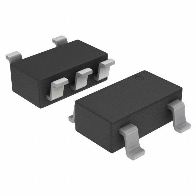
| 描述 | IC REG LDO 1.8V 0.15A 5TSOP低压差稳压器 CMOS LDO 150mA 1.8V |
| 产品分类 | |
| 品牌 | ON Semiconductor |
| 产品手册 | |
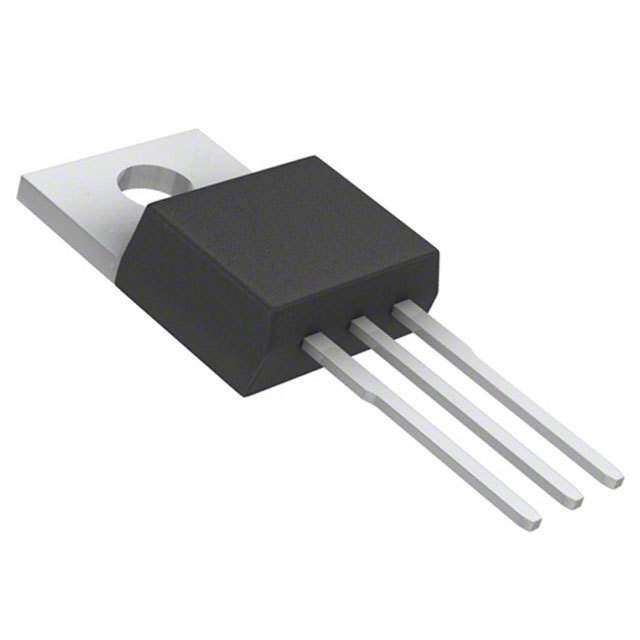
| 产品图片 |
|
| rohs | 符合RoHS无铅 / 符合限制有害物质指令(RoHS)规范要求 |
| 产品系列 | 电源管理 IC,低压差稳压器,ON Semiconductor NCP699SN18T1G- |
| 数据手册 | |
| 产品型号 | NCP699SN18T1G |
| 产品目录页面 | |
| 产品种类 | 低压差稳压器 |
| 供应商器件封装 | 5-TSOP |
| 其它名称 | NCP699SN18T1GOSTR |
| 包装 | 带卷 (TR) |
| 商标 | ON Semiconductor |
| 回动电压—最大值 | 620 mV at 150 mA |
| 安装类型 | 表面贴装 |
| 安装风格 | SMD/SMT |
| 封装 | Reel |
| 封装/外壳 | 6-TSOP(0.059",1.50mm 宽)5 引线 |
| 封装/箱体 | TSOP-5 |
| 工作温度 | -40°C ~ 85°C |
| 工厂包装数量 | 3000 |
| 最大工作温度 | + 85 C |
| 最大输入电压 | 6 V |
| 最小工作温度 | - 40 C |
| 最小输入电压 | + 2.1 V |
| 标准包装 | 3,000 |
| 电压-跌落(典型值) | 0.57V @ 150mA |
| 电压-输入 | 最高 6V |
| 电压-输出 | 1.8V |
| 电压调节准确度 | 2 % |
| 电流-输出 | 150mA |
| 电流-限制(最小值) | - |
| 稳压器拓扑 | 正,固定式 |
| 稳压器数 | 1 |
| 系列 | NCP699 |
| 线路调整率 | 3 mV / V |
| 负载调节 | 0.8 mV / mA |
| 输出电压 | 1.8 V |
| 输出电流 | 150 mA |
| 输出端数量 | 1 Output |
| 输出类型 | Fixed |


PDF Datasheet 数据手册内容提取
NCP699 150 mA CMOS Low Iq LDO with Enable in TSOP-5 The NCP699 series of fixed output LDO’s are designed for handheld communication equipment and portable battery powered applications which require low quiescent current. The NCP699 series features a very low ground current of 40 (cid:2)A, independent of load http://onsemi.com current. Each device contains a voltage reference unit, an error amplifier, a PMOS power transistor, internal resistors for setting MARKING output voltage, current limit, and temperature limit protection circuits. DIAGRAM The NCP699 has been designed to be used with low cost capacitors. 5 TSOP−5 The device is housed in the micro−miniature TSOP−5 surface mount (SOT23−5, SC59−5) xxx AYW(cid:2) package. Standard voltage versions are 1.3, 1.4, 1.5, 1.8, 2.5, 2.8, 2.9, 5 SN SUFFIX (cid:2) 3.0, 3.1, 3.3, 3.4, 4.5 and 5.0 V. Other voltages are available in 100 mV 1 CASE 483 1 steps. xxx = Specific Device Code Features A = Assembly Location • Enable Control (Active High, Supports Sub 1 V Logic) Y = Year • Very Low Ground Current of 40 (cid:2)A Typical W(cid:2) == PWbo−rFk rWeee ePkackage • Low Dropout Voltage of 340 mV at 150 mA, and 3.0 V Vout (Note: Microdot may be in either location) • Multiple Fixed Output Voltage Option • Output Voltage Accuracy of 2.0% • Operating Temperature Range of −40°C to 85°C PIN CONNECTIONS • Stable with 1 (cid:2)F Ceramic or Tantalum Capacitors • These are Pb−Free Devices Vin 1 5 Vout Typical Applications Gnd 2 • Cellular Phones Enable 3 4 N/C • Battery Powered Consumer Products • Hand−Held Instruments (Top View) • Camcorders and Cameras • Printers and Office Equipment ORDERING INFORMATION Battery or Vout See detailed ordering and shipping information in the package Unregulated + 1 5 dimensions section on page 7 of this data sheet. Voltage Cin + 1 (cid:2)F 2 Cout 1 (cid:2)F ON 3 4 OFF This device contains 86 active transistors Figure 1. Typical Application Diagram © Semiconductor Components Industries, LLC, 2009 1 Publication Order Number: January, 2009 − Rev. 8 NCP699/D
NCP699 ÁÁÁÁÁÁÁÁÁÁÁÁÁÁÁÁÁÁÁÁÁÁÁÁÁÁÁÁÁÁÁÁÁ PIN FUNCTION DESCRIPTION ÁÁÁÁÁÁÁÁÁÁÁÁÁÁÁÁÁÁÁÁÁÁÁÁÁÁÁÁÁÁÁÁÁÁÁÁÁÁÁÁÁÁÁÁÁÁÁÁÁÁÁÁÁÁÁÁÁÁÁÁÁÁÁÁÁÁÁÁ ÁÁÁÁPin ÁÁNo.ÁÁÁÁPÁÁin NÁÁamÁÁe ÁÁÁÁÁÁÁÁÁÁÁÁÁÁÁÁÁÁÁÁÁÁÁÁÁÁDeÁÁscrÁÁiptioÁÁn ÁÁÁÁÁÁÁÁÁÁÁÁÁÁÁÁÁÁÁÁÁÁ ÁÁÁÁ1ÁÁÁÁÁÁÁÁVÁÁin ÁÁÁÁÁÁPoÁÁsitivÁÁe poÁÁwer ÁÁsuppÁÁly inÁÁput ÁÁvoltaÁÁge.ÁÁÁÁÁÁÁÁÁÁÁÁÁÁÁÁÁÁÁÁÁÁÁÁÁÁÁÁÁÁÁÁÁÁ ÁÁÁÁ2ÁÁÁÁÁÁÁÁGÁÁnd ÁÁÁÁÁÁPoÁÁwerÁÁ supÁÁply gÁÁrounÁÁd. ÁÁÁÁÁÁÁÁÁÁÁÁÁÁÁÁÁÁÁÁÁÁÁÁÁÁÁÁÁÁÁÁÁÁÁÁÁÁÁÁ ÁÁ3ÁÁÁÁEnaÁbleÁÁÁThÁis inÁput iÁs usÁed toÁ plaÁce thÁe deÁviceÁ intoÁ lowÁ−powÁer sÁtandÁby. WÁheÁn thisÁ inpÁut isÁ pulleÁd loÁw, thÁe deÁviceÁ is Á disabled. If this function is not used, Enable should be connected to Vin. ÁÁÁÁÁÁÁÁÁÁÁÁÁÁÁÁÁÁÁÁÁÁÁÁÁÁÁÁÁÁÁÁÁÁÁÁÁÁÁÁÁÁÁÁÁÁÁÁÁÁÁÁÁÁÁÁÁÁÁÁÁÁÁÁÁÁÁÁÁÁ 4 N/C No internal connection. ÁÁÁÁÁÁÁÁÁÁÁÁÁÁÁÁÁÁÁÁÁÁÁÁÁÁÁÁÁÁÁÁÁÁÁÁÁÁÁÁÁÁÁÁÁÁÁÁÁÁÁÁÁÁÁÁÁÁÁÁÁÁÁÁÁÁÁÁÁÁ 5 Vout Regulated output voltage. ÁÁÁÁÁÁÁÁÁÁÁÁÁÁÁÁÁÁÁÁÁÁÁÁÁÁÁÁÁÁÁÁÁÁÁ MAXIMUM RATINGS Rating Symbol Value Unit Input Voltage Vin 2.1 to 6.0 V Enable Voltage Enable −0.3 to Vin +0.3 V Output Voltage Vout −0.3 to Vin +0.3 V Power Dissipation PD Internally Limited W Operating Junction Temperature TJ +150 °C Maximum Junction Temperature TJ(max) +150 °C Operating Ambient Temperature TA −40 to +85 °C Storage Temperature Tstg −55 to +150 °C Stresses exceeding Maximum Ratings may damage the device. Maximum Ratings are stress ratings only. Functional operation above the Recommended Operating Conditions is not implied. Extended exposure to stresses above the Recommended Operating Conditions may affect device reliability. 1. This device series contains ESD protection and exceeds the following tests: Human Body Model 2000 V per MIL−STD−883, Method 3015 Machine Model Method 200 V 2. Latch−up capability (85°C) (cid:2)200 mA DC with trigger voltage. THERMAL CHARACTERISTICS Rating Symbol Test Conditions Typical Value Unit Junction−to−Ambient R(cid:3)JA 1 oz Copper Thickness, 100 mm2 250 °C/W PSIJ−Lead 2 (cid:4)JL2 1 oz Copper Thickness, 100 mm2 68 °C/W NOTE: Single component mounted on an 80 x 80 x 1.5 mm FR4 PCB with stated copper head spreading area. Using the following boundary conditions as stated in EIA/JESD 51−1, 2, 3, 7, 12. http://onsemi.com 2
NCP699 ELECTRICAL CHARACTERISTICS (Vin = Vout(nom.) + 1.0 V, Venable = Vin, Cin = 1.0 (cid:2)F, Cout = 1.0 (cid:2)F, TA = 25°C, unless otherwise noted.) Characteristic Symbol Min Typ Max Unit Output Voltage (Iout = 10 mA, TA = −40°C to 85°C) Vout V 1.3 V 1.261 1.3 1.339 1.4 V 1.358 1.4 1.442 1.5 V 1.455 1.5 1.545 1.8 V 1.746 1.8 1.854 2.5 V 2.425 2.5 2.575 2.8 V 2.716 2.8 2.884 2.9 V 2.813 2.9 2.987 3.0 V 2.910 3.0 3.090 3.1 V 3.007 3.1 3.193 3.3 V 3.201 3.3 3.399 3.4 V 3.298 3.4 3.502 4.5 V 4.365 4.5 4.635 5.0 V 4.850 5.0 5.150 Line Regulation (Iout = 10 mA) Regline mV/V 1.3 V−4.4 V (Vin = Vout(nom.) + 1.0 V to 6.0 V) − 1.0 3.0 4.5 V−5.0 V (Vin = 5.5 V to 6.0 V) − 1.0 3.0 Load Regulation (Iout = 1.0 mA to 150 mA) Regload − 0.3 0.8 mV/mA Output Current Limit Io(nom.) mA 1.3 V−3.9 V (Vin = Vout(nom.) + 2.0 V) 150 240 − 4.0 V−5.0 V (Vin = 6.0 V) 150 240 − Dropout Voltage (Iout = 150 mA, Vin−Vout mV Measured at Vout = Vout(nom) −3.0%) 1.3 V − 800 900 1.4 V − 750 850 1.5 V − 690 750 1.8 V − 570 620 2.5 V − 400 450 2.8 V − 360 420 2.9 V − 350 420 3.0 V − 340 400 3.1 V − 330 400 3.3 V − 320 360 3.4 V − 300 360 4.5 V − 5.0 V − 240 300 Disable Current (TA = −40°C to 85°C) DIS (cid:2)A (Enable Input = 0 V) − 0.03 1.0 Ground Current (TA = −40°C to 85°C) IGND (cid:2)A (Enable Input = Vin, Iout = 1.0 mA to Io(nom.)) − 40 90 Output Short Circuit Current (Vout = 0 V) Iout(max) mA 1.3 V−3.9 V (Vin = Vout(nom.) + 2.0 V) 150 300 600 4.0 V−5.0 V (Vin = 6.0 V) 150 300 600 Output Voltage Noise (f = 100 Hz to 100 kHz) Vn (cid:2)Vrms Iout = 30 mA, Cout = 1 (cid:2)F − 100 − Ripple Rejection RR dB (f = 120 Hz, 15 mA) − 55 − (f = 1.0 kHz, 15 mA) − 50 − Enable Input Threshold Voltage (TA = −40°C to 85°C) Vth(en) V (Voltage Increasing, Output Turns On, Logic High) 0.95 − − (Voltage Decreasing, Output Turns Off, Logic Low) − − 0.3 Output Voltage Temperature Coefficient TC − (cid:2)100 − ppm/°C 3. Maximum package power dissipation limits must be observed. PD(cid:3)TJ(max) (cid:4)TA R(cid:3)JA 4. Low duty cycle pulse techniques are used during testing to maintain the junction temperature as close to ambient as possible. http://onsemi.com 3
NCP699 TYPICAL CHARACTERISTICS 450 3.015 mV) 400 V) Vin = 6.0 V E ( 350 E ( 3.010 G G Vin = 4.0 V A 300 A T T VOL 250 VOL 3.005 T T U 200 U O P 3.000 P T O 150 U R O V, DDD 15000 VVoinu t= = 4 3.0.0 V V V, out2.995 Vout = 3.0 V Iout = 150 mA Iout = 1.0 mA 0 2.990 −60 −40 −20 0 20 40 60 80 100 −60 −40 −20 0 20 40 60 80 100 TA, AMBIENT TEMPERATURE (°C) TA, AMBIENT TEMPERATURE (°C) Figure 2. Dropout Voltage vs. Temperature Figure 3. Output Voltage vs. Temperature 43 60 A) 42 A) (cid:2)NT ( 41 (cid:2)NT ( 50 RE RE 40 R 40 R U U T C 39 T C 30 N N SCE 38 SCE 20 Vout = 3.0 V QUIE 37 Vin = 4.0 V QUIE IToAu t= = 2 05 °mCA I, q 36 VIoouut t= = 0 3 m.0A V I, q 10 CCionu t= = 1 1.0.0 (cid:2) (cid:2)FF 35 0 −60 −40 −20 0 20 40 60 80 100 0 1.0 2.0 3.0 4.0 5.0 6.0 7.0 TA, AMBIENT TEMPERATURE (°C) Vin, INPUT VOLTAGE (V) Figure 4. Quiescent Current vs. Temperature Figure 5. Quiescent Current vs. Input Voltage 60 70 Vin = 4.0 V (cid:2)T (A) 50 dB) 60 CIoouut t= = 3 10. 0m (cid:2)AF EN 40 N ( 50 R O R TI 40 U C C 30 E ND REJ 30 OU 20 Vout = 3.0 V E , GRgnd 10 ITCoAiun t = == 2 135.00° C m(cid:2)FA RIPPL 1200 I Cout = 1.0 (cid:2)F 0 0 0 1.0 2.0 3.0 4.0 5.0 6.0 7.0 100 1.0k 10k 100k 1.0M Vin, INPUT VOLTAGE (V) f, FREQUENCY (Hz) Figure 6. Ground Pin Current vs. Input Voltage Figure 7. Ripple Rejection vs. Frequency http://onsemi.com 4
NCP699 TYPICAL CHARACTERISTICS 7 Hz) Vin = 4.0 V (cid:5)V/ 6 Cout = 1.0 (cid:2)F (cid:2)E ( 5 Iout = 30 mA S OI N 4 E G A 3 T L O V 2 T U P T 1 U O 0 10 100 1.0k 10k 100k 1.0M f, FREQUENCY (Hz) Figure 8. Output Noise Density Figure 9. Line Transient Response Figure 10. Load Transient Response Figure 11. Turn−on Response 3.5 V) 3.0 E ( G 2.5 A LT Iout = 1.0 mA O 2.0 V T 150 mA U P 1.5 T U O 1.0 , ut o V 0.5 TA = 25°C 0 0 1.0 2.0 3.0 4.0 5.0 6.0 Vin, INPUT VOLTAGE (V) Figure 12. Output Voltage vs. Input Voltage http://onsemi.com 5
NCP699 DEFINITIONS Load Regulation Line Regulation The change in output voltage for a change in output The change in output voltage for a change in input voltage. current at a constant temperature. The measurement is made under conditions of low dissipation or by using pulse technique such that the average Dropout Voltage chip temperature is not significantly affected. The input/output differential at which the regulator output no longer maintains regulation against further reductions in Line Transient Response input voltage. Measured when the output drops 3.0% below Typical over and undershoot response when input voltage its nominal. The junction temperature, load current, and is excited with a given slope. minimum input supply requirements affect the dropout level. Thermal Protection Maximum Power Dissipation Internal thermal shutdown circuitry is provided to protect The maximum total dissipation for which the regulator the integrated circuit in the event that the maximum junction will operate within its specifications. temperature is exceeded. When activated at typically 160°C, the regulator turns off. This feature is provided to prevent Quiescent and Ground Current failures from accidental overheating. The quiescent current is the current which flows through the ground when the LDO operates without a load on its Maximum Package Power Dissipation output: internal IC operation, bias, etc. When the LDO The maximum power package dissipation is the power becomes loaded, this term is called the Ground current. It is dissipation level at which the junction temperature reaches actually the difference between the input current (measured its maximum operating value, i.e. 125°C. Depending on the through the LDO input pin) and the output current. ambient power dissipation and thus the maximum available output current. http://onsemi.com 6
NCP699 APPLICATIONS INFORMATION A typical application circuit for the NCP699 series is Set external components, especially the output capacitor, shown in Figure 1, front page. as close as possible to the circuit, and make leads as short as possible. Input Decoupling (C ) in A 1.0 (cid:2)F capacitor either ceramic or tantalum is Thermal recommended and should be connected close to the NCP699 As power across the NCP699 increases, it might become package. Higher values and lower ESR will improve the necessary to provide some thermal relief. The maximum overall line transient response. power dissipation supported by the device is dependent TDK capacitor: C2012X5R1C105K, or C1608X5R1A105K upon board design and layout. Mounting pad configuration on the PCB, the board material and also the ambient Output Decoupling (Cout) temperature effect the rate of temperature rise for the part. The NCP699 is a stable regulator and does not require any This is stating that when the NCP699 has good thermal specific Equivalent Series Resistance (ESR) or a minimum conductivity through the PCB, the junction temperature will output current. Capacitors exhibiting ESRs ranging from a be relatively low with high power dissipation applications. few m(cid:5) up to 5.0 (cid:5) can thus safely be used. The minimum The maximum dissipation the package can handle is decoupling value is 1.0 (cid:2)F and can be augmented to fulfill given by: stringent load transient requirements. The regulator accepts ceramic chip capacitors as well as tantalum capacitors. PD(cid:3)TJ(max) (cid:4)TA Larger values improve noise rejection and load regulation R(cid:3)JA If junction temperature is not allowed above the transient response. maximum 125°C, then the NCP699 can dissipate up to TDK capacitor: C2012X5R1C105K, C1608X5R1A105K, 400 mW @ 25°C. or C3216X7R1C105K The power dissipated by the NCP699 can be calculated Enable Operation from the following equation: The enable pin will turn on the regulator when pulled high Ptot(cid:3)(cid:6)Vin*Ignd(@Iout)(cid:7)(cid:8)[Vin(cid:4)Vout]*Iout and turn off the regulator when pulled low. These limits of threshold are covered in the electrical specification section or obef tchoisn ndeatcat esdh eteot .V Iifn t.he enable is not used then the pin should VinMAX(cid:3)IgPntodt(@(cid:8)IVouotu)t(cid:8)*IoIouutt Hints If an 150 mA output current is needed then the ground Please be sure the Vin and Gnd lines are sufficiently wide. current from the data sheet is 40 (cid:2)A. For an NCP699 (3.0 V), When the impedance of these lines is high, there is a chance the maximum input voltage will then be 5.65 V. to pick up noise or cause the regulator to malfunction. ORDERING INFORMATION Nominal Device Output Voltage* Marking Package Shipping† NCP699SN13T1G 1.3 LJY NCP699SN14T1G 1.4 AA4 NCP699SN15T1G 1.5 LJP NCP699SN18T1G 1.8 LJS NCP699SN25T1G 2.5 LJT NCP699SN28T1G 2.8 LJU TSOP−5 3000 Units/ NCP699SN29T1G 2.9 ACP (Pb−Free) 7″ Tape & Reel NCP699SN30T1G 3.0 LJV NCP699SN31T1G 3.1 AAE NCP699SN33T1G 3.3 LJW NCP699SN34T1G 3.4 ACF NCP699SN45T1G 4.5 ACQ NCP699SN50T1G 5.0 LJX *Additional voltages in 100 mV steps are available upon request by contacting your ON Semiconductor representative. †For information on tape and reel specifications, including part orientation and tape sizes, please refer to our Tape and Reel Packaging Specification Brochure, BRD8011/D. http://onsemi.com 7
NCP699 PACKAGE DIMENSIONS TSOP−5 CASE 483−02 ISSUE H NOTES: 1. DIMENSIONING AND TOLERANCING PER NOTE 5 D5X ASME Y14.5M, 1994. 2. CONTROLLING DIMENSION: MILLIMETERS. 0.20 C A B 3. MAXIMUM LEAD THICKNESS INCLUDES 2X 0.10 T LEAD FINISH THICKNESS. MINIMUM LEAD THICKNESS IS THE MINIMUM THICKNESS M OF BASE MATERIAL. 2X 0.20 T 5 4 B S 4. DMIOMLEDN FSLIOANSSH ,A P ARNODT RBU DSOIO NNOST, OINRC GLUATDEE 1 2 3 BURRS. K 5. OPTIONAL CONSTRUCTION: AN L DETAIL Z ADDITIONAL TRIMMED LEAD IS ALLOWED G IN THIS LOCATION. TRIMMED LEAD NOT TO EXTEND MORE THAN 0.2 FROM BODY. A MILLIMETERS DIM MIN MAX DETAIL Z A 3.00 BSC J B 1.50 BSC C C 0.90 1.10 0.05 H SPELAATNIENG GD 0.02.595 BS0C.50 H 0.01 0.10 T J 0.10 0.26 K 0.20 0.60 SOLDERING FOOTPRINT* ML 1.02 5(cid:3) 110.5 (cid:3) 5 S 2.50 3.00 1.9 0.074 0.95 0.037 2.4 0.094 1.0 0.039 0.7 (cid:9) (cid:10) 0.028 SCALE 10:1 mm inches *For additional information on our Pb−Free strategy and soldering details, please download the ON Semiconductor Soldering and Mounting Techniques Reference Manual, SOLDERRM/D. ON Semiconductor and are registered trademarks of Semiconductor Components Industries, LLC (SCILLC). SCILLC reserves the right to make changes without further notice to any products herein. SCILLC makes no warranty, representation or guarantee regarding the suitability of its products for any particular purpose, nor does SCILLC assume any liability arising out of the application or use of any product or circuit, and specifically disclaims any and all liability, including without limitation special, consequential or incidental damages. “Typical” parameters which may be provided in SCILLC data sheets and/or specifications can and do vary in different applications and actual performance may vary over time. All operating parameters, including “Typicals” must be validated for each customer application by customer’s technical experts. SCILLC does not convey any license under its patent rights nor the rights of others. SCILLC products are not designed, intended, or authorized for use as components in systems intended for surgical implant into the body, or other applications intended to support or sustain life, or for any other application in which the failure of the SCILLC product could create a situation where personal injury or death may occur. Should Buyer purchase or use SCILLC products for any such unintended or unauthorized application, Buyer shall indemnify and hold SCILLC and its officers, employees, subsidiaries, affiliates, and distributors harmless against all claims, costs, damages, and expenses, and reasonable attorney fees arising out of, directly or indirectly, any claim of personal injury or death associated with such unintended or unauthorized use, even if such claim alleges that SCILLC was negligent regarding the design or manufacture of the part. SCILLC is an Equal Opportunity/Affirmative Action Employer. This literature is subject to all applicable copyright laws and is not for resale in any manner. PUBLICATION ORDERING INFORMATION LITERATURE FULFILLMENT: N. American Technical Support: 800−282−9855 Toll Free ON Semiconductor Website: www.onsemi.com Literature Distribution Center for ON Semiconductor USA/Canada P.O. Box 5163, Denver, Colorado 80217 USA Europe, Middle East and Africa Technical Support: Order Literature: http://www.onsemi.com/orderlit Phone: 303−675−2175 or 800−344−3860 Toll Free USA/Canada Phone: 421 33 790 2910 Fax: 303−675−2176 or 800−344−3867 Toll Free USA/Canada Japan Customer Focus Center For additional information, please contact your local Email: orderlit@onsemi.com Phone: 81−3−5773−3850 Sales Representative http://onsemi.com NCP699/D 8