ICGOO在线商城 > 集成电路(IC) > PMIC - 稳压器 - 线性 > ADP1753ACPZ-R7
 Datasheet下载
- 型号: ADP1753ACPZ-R7
- 制造商: Analog
- 库位|库存: xxxx|xxxx
- 要求:
| 数量阶梯 | 香港交货 | 国内含税 |
| +xxxx | $xxxx | ¥xxxx |
查看当月历史价格
查看今年历史价格
ADP1753ACPZ-R7产品简介:
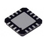
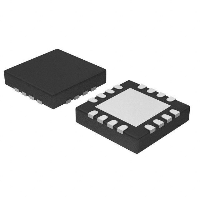
ICGOO电子元器件商城为您提供ADP1753ACPZ-R7由Analog设计生产,在icgoo商城现货销售,并且可以通过原厂、代理商等渠道进行代购。 ADP1753ACPZ-R7价格参考¥13.27-¥19.84。AnalogADP1753ACPZ-R7封装/规格:PMIC - 稳压器 - 线性, Linear Voltage Regulator IC Positive Adjustable 1 Output 0.75 V ~ 3 V 800mA 16-LFCSP-WQ (4x4)。您可以下载ADP1753ACPZ-R7参考资料、Datasheet数据手册功能说明书,资料中有ADP1753ACPZ-R7 详细功能的应用电路图电压和使用方法及教程。
ADP1753ACPZ-R7 是由 Analog Devices Inc.(ADI)生产的一款低功耗、高精度线性稳压器,属于 PMIC(电源管理集成电路)中的线性稳压器类别。以下是其主要应用场景:

 1. 便携式电子设备
   - ADP1753ACPZ-R7 的低静态电流和小封装设计使其非常适合用于电池供电的便携式设备,如:
     - 智能手机和平板电脑
     - 可穿戴设备(智能手表、健康监测器等)
     - 便携式医疗设备(血糖仪、脉搏血氧仪等)
   - 在这些应用中,其高效率和低功耗特性可以延长电池寿命。

 2. 通信设备
   - 该稳压器可用于通信设备中的电源管理,例如:
     - 蓝牙模块
     - Wi-Fi 模块
     - GPS 接收器
   - 它能够为这些模块提供稳定且精确的电压输出,确保信号传输的可靠性。

 3. 工业控制
   - 在工业自动化领域,ADP1753ACPZ-R7 可以为各种传感器和控制器供电,例如:
     - 温度传感器
     - 压力传感器
     - 数据采集系统
   - 其高精度输出电压有助于提高测量和控制的准确性。

 4. 消费类电子产品
   - 适用于需要高效电源管理的消费类电子产品,例如:
     - 数码相机
     - 音频设备(耳机放大器、音响等)
     - 游戏控制器
   - 稳定的电压输出可以提升音质或图像质量。

 5. 汽车电子
   - 虽然 ADP1753ACPZ-R7 主要面向消费级和工业级应用,但在某些非关键汽车子系统中也可以使用,例如:
     - 车载信息娱乐系统
     - 仪表盘显示模块
   - 其紧凑的设计和低噪声性能适合对空间和电磁干扰敏感的应用。

 6. 物联网 (IoT) 设备
   - ADP1753ACPZ-R7 的低功耗特性使其成为 IoT 设备的理想选择,例如:
     - 智能家居设备(温控器、安防摄像头等)
     - 无线传感器网络节点
   - 它能够有效降低功耗,延长电池续航时间。

 总结
ADP1753ACPZ-R7 的主要应用场景集中在需要低功耗、高精度电压输出的领域,包括便携式设备、通信模块、工业控制、消费类电子产品以及 IoT 设备等。其出色的性能和紧凑的封装设计使其成为现代电子产品的理想电源解决方案。
| 参数 | 数值 |
| 产品目录 | 集成电路 (IC)半导体 |
| 描述 | IC REG LDO ADJ 0.8A 16LFCSP线性稳压器 800mA Low-Vin Adj-Vout LDO |
| 产品分类 | |
| 品牌 | Analog Devices |
| 产品手册 | |
| 产品图片 |
|
| rohs | 符合RoHS无铅 / 符合限制有害物质指令(RoHS)规范要求 |
| 产品系列 | 电源管理 IC,线性稳压器,Analog Devices ADP1753ACPZ-R7- |
| 数据手册 | |
| 产品型号 | ADP1753ACPZ-R7 |
| PCN组件/产地 | |
| PSRR/纹波抑制—典型值 | 65 dB |
| 产品种类 | |
| 供应商器件封装 | 16-LFCSP-VQ (4x4) |
| 其它名称 | ADP1753ACPZ-R7-ND |
| 包装 | 带卷 (TR) |
| 商标 | Analog Devices |
| 安装类型 | 表面贴装 |
| 安装风格 | SMD/SMT |
| 封装 | Reel |
| 封装/外壳 | 16-VQFN 裸露焊盘,CSP |
| 封装/箱体 | LFCSP-16 |
| 工作温度 | -40°C ~ 125°C |
| 工厂包装数量 | 1500 |
| 最大工作温度 | + 125 C |
| 最大输入电压 | 3.6 V |
| 最小工作温度 | - 40 C |
| 最小输入电压 | 1.6 V |
| 标准包装 | 1,500 |
| 电压-跌落(典型值) | 0.07V @ 800mA |
| 电压-输入 | 1.6 V ~ 3.6 V |
| 电压-输出 | 0.75 V ~ 3 V |
| 电流-输出 | 800mA |
| 电流-限制(最小值) | 1A |
| 稳压器拓扑 | 正,可调式 |
| 稳压器数 | 1 |
| 系列 | ADP1753 |
| 线路调整率 | 3 % / V |
| 视频文件 | http://www.digikey.cn/classic/video.aspx?PlayerID=1364138032001&width=640&height=505&videoID=2245193149001 |
| 负载调节 | 0.8 % / A |
| 输出电压 | 0.75 V to 3 V |
| 输出电流 | 800 mA |
| 输出端数量 | 5 |
| 输出类型 | Adjustable |
| 配用 | /product-detail/zh/AD-FMCADC2-EBZ/AD-FMCADC2-EBZ-ND/4915055 |


- 商务部:美国ITC正式对集成电路等产品启动337调查
- 曝三星4nm工艺存在良率问题 高通将骁龙8 Gen1或转产台积电
- 太阳诱电将投资9.5亿元在常州建新厂生产MLCC 预计2023年完工
- 英特尔发布欧洲新工厂建设计划 深化IDM 2.0 战略
- 台积电先进制程称霸业界 有大客户加持明年业绩稳了
- 达到5530亿美元!SIA预计今年全球半导体销售额将创下新高
- 英特尔拟将自动驾驶子公司Mobileye上市 估值或超500亿美元
- 三星加码芯片和SET,合并消费电子和移动部门,撤换高东真等 CEO
- 三星电子宣布重大人事变动 还合并消费电子和移动部门
- 海关总署:前11个月进口集成电路产品价值2.52万亿元 增长14.8%


PDF Datasheet 数据手册内容提取
0.8 A, Low V , Low Dropout IN Linear Regulator Data Sheet ADP1752/ADP1753 FEATURES TYPICAL APPLICATION CIRCUITS Maximum output current: 0.8 A VIN = 1.8V VOUT = 1.5V Input voltage range: 1.6 V to 3.6 V 4.7µF 4.7µF Low shutdown current: <2 µA 16 15 14 13 Very low dropout voltage: 70 mV at 0.8 A load VIN VIN VOUTVOUT Initial accuracy: ±1% 1VIN VOUT12 Accuracy over line, load, and temperature: ±2% ADP1752 100kΩ 2VIN VOUT11 TOP VIEW 7 fixed output voltage options with soft start (Not to Scale) 0.75 V to 2.5 V (ADP1752) 3VIN VOUT10 PG Adjustable output voltage option with soft start 4EN SENSE9 0.75 V to 3.3 V (ADP1753) PG GND SS NC High PSRR 5 6 7 8 65 dB at 1 kHz 65 dB at 10 kHz 10nF 07718-001 54 dB at 100 kHz Figure 1. ADP1752 with Fixed Output Voltage, 1.5 V 23 μV rms at 0.75 V output Stable with small 4.7 µF ceramic output capacitor VIN = 1.8V VOUT = 0.5V(1 + R1/R2) Excellent load and line transient response 4.7µF 4.7µF Current-limit and thermal overload protection 16 15 14 13 VIN VIN VOUTVOUT Power-good indicator 1VIN VOUT12 Logic-controlled enable ADP1753 Reverse current protection 100kΩ 2VIN TOP VIEW VOUT11 (Not to Scale) 3VIN VOUT10 APPLICATIONS R1 PG 4EN ADJ 9 Server computers PG GND SS NC R2 Memory components 5 6 7 8 Telecommunications equipment NDSetPw/FoPrGk Aeq/muiipcrmopenrot cessor supplies 10nF 07718-002 Figure 2. ADP1753 with Adjustable Output Voltage, 0.75 V to 3.3 V Instrumentation equipment/data acquisition systems GENERAL DESCRIPTION The ADP1752/ADP1753 are low dropout (LDO) CMOS linear voltages that range from 0.75 V to 3.3 V via an external divider. regulators that operate from 1.6 V to 3.6 V and provide up to The ADP1752/ADP1753 allow an external soft start capacitor 800 mA of output current. These low V /V LDOs are ideal to be connected to program the startup. A digital power-good IN OUT for regulation of nanometer FPGA geometries operating from output allows power system monitors to check the health of the 2.5 V down to 1.8 V I/O rails, and for powering core voltages output voltage. down to 0.75 V. Using an advanced proprietary architecture, The ADP1752/ADP1753 are available in a 16-lead, 4 mm × 4 mm they provide high power supply rejection ratio (PSRR) and low LFCSP, making them not only very compact solutions, but also noise, and achieve excellent line and load transient response providing excellent thermal performance for applications that with only a small 4.7 µF ceramic output capacitor. require up to 800 mA of output current in a small, low profile The ADP1752 is available in seven fixed output voltage options. footprint. The ADP1753 is the adjustable version, which allows output Rev. H Document Feedback Information furnished by Analog Devices is believed to be accurate and reliable. However, no responsibility is assumed by Analog Devices for its use, nor for any infringements of patents or other One Technology Way, P.O. Box 9106, Norwood, MA 02062-9106, U.S.A. rights of third parties that may result from its use. Specifications subject to change without notice. No license is granted by implication or otherwise under any patent or patent rights of Analog Devices. Tel: 781.329.4700 ©2008–2015 Analog Devices, Inc. All rights reserved. Trademarks and registered trademarks are the property of their respective owners. Technical Support www.analog.com
ADP1752/ADP1753 Data Sheet TABLE OF CONTENTS Features .............................................................................................. 1 Soft Start Function (ADP1752/ADP1753) ............................. 11 Adjustable Output Voltage (ADP1753) ................................... 12 Applications ....................................................................................... 1 Typical Application Circuits ............................................................ 1 Enable Feature ............................................................................ 12 Power-Good Feature .................................................................. 12 General Description ......................................................................... 1 Revision History ............................................................................... 2 Reverse Current Protection Feature ........................................ 13 Specifications ..................................................................................... 3 Applications Information .............................................................. 14 Capacitor Selection .................................................................... 14 Input and Output Capacitor, Recommended Specifications .. 4 Absolute Maximum Ratings ............................................................ 5 Undervoltage Lockout ............................................................... 15 Current-Limit and Thermal Overload Protection ................. 15 Thermal Data ................................................................................ 5 Thermal Resistance ...................................................................... 5 Thermal Considerations ............................................................ 15 PCB Layout Considerations ...................................................... 18 ESD Caution .................................................................................. 5 Pin Configurations and Function Descriptions ........................... 6 Outline Dimensions ....................................................................... 19 Typical Performance Characteristics ............................................. 7 Ordering Guide .......................................................................... 19 Theory of Operation ...................................................................... 11 REVISION HISTORY 1/15—Rev. G to Rev. H 9/12—Rev. B to Rev. C Changes to Ordering Guide .......................................................... 19 Changes to Table 3 ............................................................................. 5 Changes to Ordering Guide .......................................................... 19 4/14—Rev. F to Rev. G 2/10—Rev. A to Rev. B Changes to Figure 1 and Figure 2 ................................................... 1 Change to Table 4 ............................................................................. 5 Changes to Table 4 ............................................................................. 5 Changes to Figure 3 and Figure 4 ................................................... 6 Changes to Ordering Guide .......................................................... 19 Updated Outline Dimensions ....................................................... 19 4/09—Rev. 0 to Rev. A Changes to Ordering Guide .......................................................... 19 Changes to Adjustable Output Voltage Accuracy (ADP1753) 1/14—Rev. E to Rev. F Parameter, Table 1 ............................................................................. 3 Changes to Ordering Guide .......................................................... 19 Changes to Table 3 ............................................................................. 5 6/13—Rev. D to Rev. E 10/08—Revision 0: Initial Version Changed Adjustable Output Voltage Option with Soft Start (ADP1755) from 0.75 V to 3.0 V to 0.75 V to 3.3 V (Throughout) .................................................................................... 1 Updated Outline Dimensions ....................................................... 19 12/12—Rev. C to Rev. D Added Junction Temperature of 150°C, Table 3 ........................... 5 Rev. H | Page 2 of 20
Data Sheet ADP1752/ADP1753 SPECIFICATIONS V = (V + 0.4 V) or 1.6 V (whichever is greater), I = 10 mA, C = C = 4.7 µF, T = 25°C, unless otherwise noted. IN OUT OUT IN OUT A Table 1. Parameter Symbol Test Conditions/Comments Min Typ Max Unit INPUT VOLTAGE RANGE V T = −40°C to +125°C 1.6 3.6 V IN J OPERATING SUPPLY CURRENT1 I I = 500 μA 90 µA GND OUT I = 100 mA 400 µA OUT I = 100 mA, T = −40°C to +125°C 800 µA OUT J I = 0.8 A 0.9 mA OUT I = 0.8 A, T = −40°C to +125°C 1.2 mA OUT J SHUTDOWN CURRENT IGND-SD EN = GND, VIN = 1.6 V 2 6 µA EN = GND, VIN = 1.6 V, TJ = −40°C to +85°C 30 µA EN = GND, VIN = 3.6 V, TJ = −40°C to +85°C 100 µA OUTPUT VOLTAGE ACCURACY Fixed Output Voltage Accuracy V I = 10 mA −1 +1 % OUT OUT (ADP1752) I = 10 mA to 0.8 A −1.5 +1.5 % OUT 10 mA < I < 0.8 A, T = −40°C to +125°C −2 +2 % OUT J Adjustable Output Voltage Accuracy V I = 10 mA 0.495 0.5 0.505 V ADJ OUT (ADP1753)2 I = 10 mA to 0.8 A 0.492 0.508 V OUT 10 mA < I < 0.8 A, T = −40°C to +125°C 0.490 0.510 V OUT J LINE REGULATION ∆V /∆V V = (V + 0.4 V) to 3.6 V, T = −40°C to +125°C −0.3 +0.3 %/V OUT IN IN OUT J LOAD REGULATION3 ∆V /∆I I = 10 mA to 0.8 A, T = −40°C to +125°C 0.8 %/A OUT OUT OUT J DROPOUT VOLTAGE4 V I = 100 mA, V ≥ 1.8 V 10 mV DROPOUT OUT OUT I = 100 mA, V ≥ 1.8 V, T = −40°C to +125°C 16 mV OUT OUT J I = 0.8 A, V ≥ 1.8 V 70 mV OUT OUT I = 0.8 A, V ≥ 1.8 V, T = −40°C to +125°C 140 mV OUT OUT J START-UP TIME5 t C = 0 nF, I = 10 mA 200 µs START-UP SS OUT C = 10 nF, I = 10 mA 5.2 ms SS OUT CURRENT-LIMIT THRESHOLD6 I 1 1.4 5 A LIMIT THERMAL SHUTDOWN Thermal Shutdown Threshold TSSD TJ rising 150 °C Thermal Shutdown Hysteresis TSSD-HYS 15 °C PG OUTPUT LOGIC LEVEL PG Output Logic High PG 1.6 V ≤ V ≤ 3.6 V, I < 1 µA 1.0 V HIGH IN OH PG Output Logic Low PG 1.6 V ≤ V ≤ 3.6 V, I < 2 mA 0.4 V LOW IN OL PG Output Delay from EN Transition 1.6 V ≤ V ≤ 3.6 V, C = 10 nF 5.5 ms IN SS Low to High PG OUTPUT THRESHOLD Output Voltage Falling PG 1.6 V ≤ V ≤ 3.6 V −10 % FALL IN Output Voltage Rising PG 1.6 V ≤ V ≤ 3.6 V −6.5 % RISE IN EN INPUT EN Input Logic High V 1.6 V ≤ V ≤ 3.6 V 1.2 V IH IN EN Input Logic Low V 1.6 V ≤ V ≤ 3.6 V 0.4 V IL IN EN Input Leakage Current V EN = VIN or GND 0.1 1 µA I-LEAKAGE UNDERVOLTAGE LOCKOUT UVLO Input Voltage Rising UVLO T = −40°C to +125°C 1.58 V RISE J Input Voltage Falling UVLO T = −40°C to +125°C 1.25 V FALL J Hysteresis UVLO T = 25°C 100 mV HYS J SOFT START CURRENT I 1.6 V ≤ V ≤ 3.6 V 0.6 0.9 1.2 µA SS IN ADJ INPUT BIAS CURRENT (ADP1753) ADJ 1.6 V ≤ V ≤ 3.6 V, T = −40°C to +125°C 10 150 nA I-BIAS IN J SENSE INPUT BIAS CURRENT SNS 1.6 V ≤ V ≤ 3.6 V 10 µA I-BIAS IN Rev. H | Page 3 of 20
ADP1752/ADP1753 Data Sheet Parameter Symbol Test Conditions/Comments Min Typ Max Unit OUTPUT NOISE OUT 10 Hz to 100 kHz, V = 0.75 V 23 µV rms NOISE OUT 10 Hz to 100 kHz, V = 2.5 V 65 µV rms OUT POWER SUPPLY REJECTION RATIO PSRR VIN = VOUT + 1 V, IOUT = 10 mA 1 kHz, V = 0.75 V 65 dB OUT 1 kHz, VOUT = 2.5 V 56 dB 10 kHz, VOUT = 0.75 V 65 dB 10 kHz, VOUT = 2.5 V 56 dB 100 kHz, VOUT = 0.75 V 54 dB 100 kHz, VOUT = 2.5 V 51 dB 1 Minimum output load current is 500 μA. 2 Accuracy when VOUT is connected directly to ADJ. When VOUT voltage is set by external feedback resistors, absolute accuracy in adjust mode depends on the tolerances of resistors used. 3 Based on an end-point calculation using 10 mA and 0.8 A loads. See Figure 6 for typical load regulation performance. 4 Dropout voltage is defined as the input to output voltage differential when the input voltage is set to the nominal output voltage. This applies only to output voltages above 1.6 V. 5 Start-up time is defined as the time between the rising edge of EN to VOUT being at 95% of its nominal value. 6 Current-limit threshold is defined as the current at which the output voltage drops to 90% of the specified typical value. For example, the current limit for a 1.0 V output voltage is defined as the current that causes the output voltage to drop to 90% of 1.0 V, or 0.9 V. INPUT AND OUTPUT CAPACITOR, RECOMMENDED SPECIFICATIONS Table 2. Parameter Symbol Test Conditions/Comments Min Typ Max Unit MINIMUM INPUT AND OUTPUT CAPACITANCE1 C T = −40°C to +125°C 3.3 µF MIN A CAPACITOR ESR R T = −40°C to +125°C 0.001 0.1 Ω ESR A 1 The minimum input and output capacitance should be greater than 3.3 µF over the full range of operating conditions. The full range of operating conditions in the application must be considered during device selection to ensure that the minimum capacitance specification is met. X7R and X5R type capacitors are recommended; Y5V and Z5U capacitors are not recommended for use with this LDO. Rev. H | Page 4 of 20
Data Sheet ADP1752/ADP1753 ABSOLUTE MAXIMUM RATINGS Junction-to-ambient thermal resistance (θ ) of the package is Table 3. JA based on modeling and calculation using a 4-layer board. The Parameter Rating junction-to-ambient thermal resistance is highly dependent on VIN to GND −0.3 V to +4.0 V the application and board layout. In applications where high VOUT to GND −0.3 V to V IN maximum power dissipation exists, close attention to thermal EN to GND −0.3 V to V IN board design is required. The value of θ may vary, depending SS to GND −0.3 V to V JA IN on PCB material, layout, and environmental conditions. The PG to GND −0.3 V to +4.0 V specified values of θ are based on a 4-layer, 4 in × 3 in circuit SENSE/ADJ to GND −0.3 V to V JA IN board. Refer to JEDEC JESD51-7 for detailed information about Storage Temperature Range −65°C to +150°C board construction. For more information, see the AN-772 Junction Temperature Range −40°C to +125°C Application Note, A Design and Manufacturing Guide for the Junction Temperature 150°C Lead Frame Chip Scale Package (LFCSP) at www.analog.com. Soldering Conditions JEDEC J-STD-020 Ψ is the junction-to-board thermal characterization parameter Stresses at or above those listed under Absolute Maximum JB with units of °C/W. Ψ of the package is based on modeling and JB Ratings may cause permanent damage to the product. This is a calculation using a 4-layer board. The JESD51-12 document, stress rating only; functional operation of the product at these Guidelines for Reporting and Using Electronic Package Thermal or any other conditions above those indicated in the operational Information, states that thermal characterization parameters are section of this specification is not implied. Operation beyond not the same as thermal resistances. Ψ measures the component JB the maximum operating conditions for extended periods may power flowing through multiple thermal paths rather than affect product reliability. through a single path as in thermal resistance, θ . Therefore, JB THERMAL DATA Ψ thermal paths include convection from the top of the package JB Absolute maximum ratings apply individually only, not in as well as radiation from the package, factors that make ΨJB more combination. The ADP1752/ADP1753 may be damaged if the useful in real-world applications. Maximum junction temperature junction temperature limits are exceeded. Monitoring ambient (TJ) is calculated from the board temperature (TB) and the power temperature does not guarantee that TJ is within the specified dissipation (PD) using the following formula: temperature limits. In applications with high power dissipation T = T + (P × Ψ ) J B D JB and poor thermal resistance, the maximum ambient tempera- Refer to the JEDEC JESD51-8 and JESD51-12 documents for more ture may need to be derated. In applications with moderate detailed information about Ψ . JB power dissipation and low PCB thermal resistance, the maximum THERMAL RESISTANCE ambient temperature can exceed the maximum limit as long as the junction temperature is within specification limits. The θ and Ψ are specified for the worst-case conditions, that is, a JA JB junction temperature (TJ) of the device is dependent on the device soldered in a circuit board for surface-mount packages. ambient temperature (T ), the power dissipation of the device A (P ), and the junction-to-ambient thermal resistance of the Table 4. Thermal Resistance D package (θJA). TJ is calculated using the following formula: Package Type θJA ΨJB Unit 16-Lead LFCSP with Exposed Pad (CP-16-23) 42 25.5 °C/W T = T + (P × θ ). J A D JA ESD CAUTION Rev. H | Page 5 of 20
ADP1752/ADP1753 Data Sheet PIN CONFIGURATIONS AND FUNCTION DESCRIPTIONS T T T T VIN VIN VOU VOU VIN VIN VOU VOU 6 5 4 3 6 5 4 3 1 1 1 1 1 1 1 1 VIN 1 12 VOUT VIN 1 12 VOUT VIN 2 ADP1752 11 VOUT VIN 2 ADP1753 11 VOUT VIN 3 TOP VIEW 10 VOUT VIN 3 TOP VIEW 10 VOUT (Not to Scale) (Not to Scale) EN 4 9 SENSE EN 4 9 ADJ 5 6 7 8 5 6 7 8 G D S C G D S C P N S N P N S N G G NOTES NOTES 1.NC = NO CONNECT. 1.NC = NO CONNECT. 2.THE EXPOSED PAD ON THE BOTTOM OF THE LFCSP ENHANCES 2.THE EXPOSED PAD ON THE BOTTOM OF THE LFCSP ENHANCES TIBNHESE CIDROEMN ATNLHE EPC EPTREAFDCO KTRAOMG TAEHN. EICT GE I SRA ORNUEDNC ISDO MEPLLMEAECNNTEDR EOICDNA TTLHHLAEYT BC TOOHANERN EDEX.CPTOESDE TDO P GANDD 07718-003 TIBNHESE CIDROEMN ATNLHE EPC EPTREAFDCO KTRAOMG TAEHN. EICT GE I SRA ORNUEDNC ISDO MEPLLMEAECNNTEDR EOICDNA TTLHHLAEYT BC TOOHANERN EDEX.CPTOESDE TDO P GANDD 07718-004 Figure 3. ADP1752 Pin Configuration Figure 4. ADP1753 Pin Configuration Table 5. Pin Function Descriptions ADP1752 ADP1753 Pin No. Pin No. Mnemonic Description 1, 2, 3, 15, 16 1, 2, 3, 15, 16 VIN Regulator Input Supply. Bypass VIN to GND with a 4.7 µF or greater capacitor. Note that all five VIN pins must be connected to the source. 4 4 EN Enable Input. Drive EN high to turn on the regulator; drive it low to turn off the regulator. For automatic startup, connect EN to VIN. 5 5 PG Power Good. This open-drain output requires an external pull-up resistor to VIN. If the part is in shutdown mode, current-limit mode, thermal shutdown, or if it falls below 90% of the nominal output voltage, PG immediately transitions low. 6 6 GND Ground. 7 7 SS Soft Start. A capacitor connected to this pin determines the soft start time. 8 8 NC Not Connected. No internal connection. 9 N/A SENSE Sense. This pin measures the actual output voltage at the load and feeds it to the error amplifier. Connect SENSE as close as possible to the load to minimize the effect of IR drop between the regulator output and the load. N/A 9 ADJ Adjust. A resistor divider from VOUT to ADJ sets the output voltage. 10, 11, 12, 10, 11, 12, VOUT Regulated Output Voltage. Bypass VOUT to GND with a 4.7 µF or greater capacitor. Note that 13, 14 13, 14 all five VOUT pins must be connected to the load. 17 (EPAD) 17 (EPAD) Exposed The exposed pad on the bottom of the LFCSP package enhances thermal performance and paddle is electrically connected to GND inside the package. It is recommended that the exposed (EPAD) pad be connected to the ground plane on the board. Rev. H | Page 6 of 20
Data Sheet ADP1752/ADP1753 TYPICAL PERFORMANCE CHARACTERISTICS V = 1.9 V, V = 1.5 V, I = 10 mA, C = 4.7 µF, C = 4.7 µF, T = 25°C, unless otherwise noted. IN OUT OUT IN OUT A 1.520 1000 LOAD = 800mA 900 1.515 800 AGE (V) 11..551005 LOAD = 10mA ENT (µA) 760000 LOAD = 400mA OLT 1.500 LOAD = 100mA URR 500 OUTPUT V 1.495 LOAD = 4L0O0AmDA = 800mA ROUND C 430000 LOAD = 100mA 1.490 G LOAD = 10mA 200 1.485 100 1.480 –40 JU–N5CTION TEM25PERATURE8 (5°C) 125 07718-105 0 –40 JU–N5CTION TEM25PERATURE8 (5°C) 125 07718-108 Figure 5. Output Voltage vs. Junction Temperature Figure 8. Ground Current vs. Junction Temperature 1.520 1000 900 1.515 800 AGE (V) 11..551005 ENT (µA) 760000 T R OL 1.500 UR 500 V C UTPUT 1.495 OUND 400 O R 300 1.490 G 200 1.485 100 1.480 0 10 LOAD CU1R0R0ENT (mA) 1k 07718-106 10 LOAD CU1R0R0ENT (mA) 1k 07718-109 Figure 6. Output Voltage vs. Load Current Figure 9. Ground Current vs. Load Current 1.520 1000 900 1.515 LOAD = 800mA 800 AGE (V) 11..551005 LOAD = 10mA LOAD = 100mA ENT (µA) 760000 LOAD = 400mA T R OL 1.500 UR 500 V C UTPUT 1.495 LOAD = 400mA LOAD = 800mA OUND 400 LOAD = 100mA O R 300 1.490 G 200 LOAD = 10mA 1.485 100 1.480 0 1.8 2.0 2.2 2.4INPUT2 .V6OLT2A.8GE (V3).0 3.2 3.4 3.6 07718-107 1.8 2.0 2.2 2.4INPUT2 .V6OLT2A.8GE (V3).0 3.2 3.4 3.6 07718-110 Figure 7. Output Voltage vs. Input Voltage Figure 10. Ground Current vs. Input Voltage Rev. H | Page 7 of 20
ADP1752/ADP1753 Data Sheet 100 4500 1.9V LOAD = 10mA 90 2.0V 4000 LOAD = 100mA 2.4V LOAD = 400mA NT (µA) 7800 233...606VVV T (µA) 33500000 LOAD = 800mA RE 60 EN R R 2500 U R C 50 U WN D C 2000 UTDO 4300 ROUN 1500 H G S 1000 20 10 500 0 0 –40 –15 TE1M0PERATURE3 5(°C) 60 85 07718-111 2.3 2.4 INP2U.5T VOLTAG2E.6 (V) 2.7 2.8 07718-114 Figure 11. Shutdown Current vs. Temperature at Various Input Voltages Figure 14. Ground Current vs. Input Voltage (in Dropout), VOUT = 2.5 V 0.08 T 0.07 ILOAD V)0.06 E ( G0.05 1 A T 1mA TO 800mA LOAD STEP, 2.5A/µs, 500mA/DIV L VO0.04 POUT 0.03 1.6V 2 VOUT O 50mV/DIV R D0.02 2.5V 0.01 VIN = 3.6V VOUT = 1.5V 01 1L0OAD CURRENT (mA10)0 1k 07718-112 CH1 500mA ΩBWCH2 50mV BWMT 1 01µ0.s20%A CH1 380mA 07718-115 Figure 12. Dropout Voltage vs. Load Current, VOUT = 1.6 V, 2.5 V Figure 15. Load Transient Response, CIN = 4.7 µF, COUT = 4.7 µF 2.60 T 2.55 ILOAD 2.50 V) E ( G 2.45 1 A T 1mA TO 800mA LOAD STEP, 2.5A/µs, 500mA/DIV L O 2.40 V T U TP 2.35 2 VOUT U O 2.30 20mV/DIV LOAD = 10mA LOAD = 100mA 2.25 LOAD = 400mA VIN = 3.6V LOAD = 800mA VOUT = 1.5V 2.20 2.3 2.4 INP2U.5T VOLTAG2E.6 (V) 2.7 2.8 07718-113 CH1 500mA ΩBWCH2 20mV BWMT 1 01µ0.s20%A CH1 530mA 07718-116 Figure 13. Output Voltage vs. Input Voltage (in Dropout), VOUT = 2.5 V Figure 16. Load Transient Response, CIN = 22 µF, COUT = 22 µF Rev. H | Page 8 of 20
Data Sheet ADP1752/ADP1753 0 T VIN –10 –20 3V TO 3.5V INPUT VOLTAGE STEP, 2V/µs –30 B) –40 d R ( –50 R S VOUT P –60 2 2mV/DIV –70 –80 800mA 400mA VOUT = 1.5V –90 100mA CIN = COUT = 4.7µF 10mA 1 CH1 500mVBW CH2 2.0mV BWMT 1 09µ.4s0%A CH4 800mA 07718-117 –10010 100 1kFREQU1E0NkCY (Hz1)00k 1M 10M 07718-120 Figure 17. Line Transient Response, Load Current = 800 mA Figure 20. Power Supply Rejection Ratio vs. Frequency, VOUT = 0.75 V, VIN = 1.75 V 70 0 2.5V –10 60 –20 50 –30 OISE (µV rms) 4300 1.5V PSRR (dB) –––456000 N –70 20 0.75V –80 LOAD = 800mA 10 LOAD = 400mA –90 LOAD = 100mA LOAD = 10mA 00.0001 0.001 LOAD C0U.R01RENT (A) 0.1 1 07718-118 –10010 100 1kFREQU1E0NkCY (Hz1)00k 1M 10M 07718-121 Figure 18. Noise vs. Load Current and Output Voltage Figure 21. Power Supply Rejection Ratio vs. Frequency, VOUT = 1.5 V, VIN = 2.5 V 10 0 –10 V/ Hz) –20 µ TY ( 1 –30 NSI B) –40 E d TRAL D 1.5V 2.5V PSRR ( ––5600 C SPE 0.1 –70 E OIS 0.75V –80 LOAD = 800mA N LOAD = 400mA –90 LOAD = 100mA LOAD = 10mA 0.0110 100 FREQUE1NkCY (Hz) 10k 100k 07718-119 –10010 100 1kFREQU1E0NkCY (Hz1)00k 1M 10M 07718-122 Figure 19. Noise Spectral Density vs. Output Voltage, ILOAD = 10 mA Figure 22. Power Supply Rejection Ratio vs. Frequency, VOUT = 2.5 V, VIN = 3.5 V Rev. H | Page 9 of 20
ADP1752/ADP1753 Data Sheet 0 1.5V/800mA 1.5V/10mA –10 2.5V/800mA 2.5V/10mA 0.75V/800mA 0.75V/10mA –20 –30 B) d –40 R ( R S –50 P –60 –70 –80 –90 10 100 1kFREQU1E0NkCY (Hz1)00k 1M 10M 07718-123 Figure 23. Power Supply Rejection Ratio vs. Frequency and Output Voltage Rev. H | Page 10 of 20
Data Sheet ADP1752/ADP1753 THEORY OF OPERATION The ADP1752 is available in seven fixed output voltage options The ADP1752/ADP1753 are low dropout linear regulators that between 0.75 V and 2.5 V. The ADP1752 allows for connection use an advanced, proprietary architecture to provide high power of an external soft start capacitor that controls the output voltage supply rejection ratio (PSRR) and excellent line and load transient ramp during startup. The ADP1753 is the adjustable version response with only a small 4.7 µF ceramic output capacitor. with an output voltage that can be set to a value between 0.75 V Both devices operate from a 1.6 V to 3.6 V input rail and and 3.3 V by an external voltage divider. Both devices are con- provide up to 0.8 A of output current. Supply current in trolled by an enable pin (EN). shutdown mode is typically 2 µA. SOFT START FUNCTION (ADP1752/ADP1753) ADP1752 REVPERROSTEE PCOTLIOANRITY For applications that require a controlled startup, the ADP1752/ ADP1753 provide a programmable soft start function. The VIN VOUT programmable soft start is useful for reducing inrush current UVLO upon startup and for providing voltage sequencing. To implement soft start, connect a small ceramic capacitor from SS to GND. GND Upon startup, a 0.9 µA current source charges this capacitor. SHORT-CIRCUIT AND THERMAL PROTECTION SENSE The ADP1752/ADP1753 start-up output voltage is limited by the voltage at SS, providing a smooth ramp-up to the nominal R1 output voltage. The soft start time is calculated as follows: PG 0.5V REF R2 t = V × (C /I ) (1) SS REF SS SS PG DETECT 0.9µA where: EN SHUTDOWN SS 07718-019 VtCSSR Ei Fsi s it sht htehe s eso o0ftf. t5s stVatar rrt etp fceearrpeioandcci.et avnocltea fgreo.m SS to GND. Figure 24. ADP1752 Internal Block Diagram SS I is the current sourced from SS (0.9 µA). SS When the ADP1752/ADP1753 are disabled (using EN), the soft REVERSE POLARITY ADP1753 PROTECTION start capacitor is discharged to GND through an internal 100 Ω VIN VOUT resistor. 2.50 UVLO 2.25 EN GND SHORT-CIRCUIT 2.00 AND THERMAL PROTECTION 1.75 PG 0R.E5VF ADJ TAGE (V) 11..2550 14n.7FnF L PG VO 1.00 DETECT 10nF 0.9µA 0.75 SS EN SHUTDOWN 07718-020 00..2550 Figure 25. ADP1753 Internal Block Diagram 0 Internally, the ADP1752/ADP1753 consist of a reference, an error 0 2 4TIME (ms)6 8 10 07718-021 amplifier, a feedback voltage divider, and a PMOS pass transistor. Figure 26. VOUT Ramp-Up with External Soft Start Capacitor Output current is delivered via the PMOS pass transistor, which is controlled by the error amplifier. The error amplifier compares the reference voltage with the feedback voltage from the output and amplifies the difference. If the feedback voltage is lower than the reference voltage, the gate of the PMOS device is pulled lower, allowing more current to pass and increasing the output voltage. If the feedback voltage is higher than the reference voltage, the gate of the PMOS device is pulled higher, allowing less current to pass and decreasing the output voltage. Rev. H | Page 11 of 20
ADP1752/ADP1753 Data Sheet The EN pin active/inactive thresholds are derived from the VIN T EN voltage. Therefore, these thresholds vary with changing input voltage. Figure 29 shows typical EN active/inactive thresholds 1 when the input voltage varies from 1.6 V to 3.6 V. 1.1 1.0 VOUT V) 0.9 LD ( EN ACTIVE O H 2 500mV/DIV VCOINU =T =C O1U.5TV = 4.7µF HRES 0.8 EN INACTIVE T CH1 2.0V BW CH2 500mV BW MT 4 09µ.8s% A CH1 920mV 07718-022 EN 0.7 Figure 27. VOUT Ramp-Up with Internal Soft Start 0.6 ADJUSTABLE OUTPUT VOLTAGE (ADP1753) 0.5 T3.h3e V o uratpnugte .v Tolhtea goeu otpf utht ev oAltDagPe1 7is5 s3e ct abny bceo nsente octvienrg a a 0 r.e7s5i sVti vteo 1.6 1.8 2.0 2.2INP2U.4T VO2.L6TAG2E.8 (V)3.0 3.2 3.4 3.6 07718-024 Figure 29. Typical EN Pin Thresholds vs. Input Voltage voltage divider from VOUT to ADJ. The output voltage is calcu- lated using the following equation: POWER-GOOD FEATURE VOUT = 0.5 V × (1 + R1/R2) (2) The ADP1752/ADP1753 provide a power-good pin, PG, to where: indicate the status of the output. This open-drain output R1 is the resistor from VOUT to ADJ. requires an external pull-up resistor to VIN. If the part is in R2 is the resistor from ADJ to GND. shutdown, in current limit mode, in thermal shutdown, or if it falls below 90% of the nominal output voltage, PG immediately The maximum bias current into ADJ is 150 nA. Therefore, to transitions low. During soft start, the rising threshold of the achieve less than 0.5% error due to the bias current, use values power-good signal is 93.5% of the nominal output voltage. less than 60 kΩ for R2. The open-drain output is held low when the ADP1752/ADP1753 ENABLE FEATURE have sufficient input voltage to turn on the internal PG transistor. The ADP1752/ADP1753 use the EN pin to enable and disable An optional soft start delay can be detected. The PG transistor the VOUT pin under normal operating conditions. As shown in is terminated via a pull-up resistor to V or V . OUT IN Figure 28, when a rising voltage on EN crosses the active Power-good accuracy is 93.5% of the nominal regulator output threshold, VOUT turns on. When a falling voltage on EN voltage when this voltage is rising, with a 90% trip point when crosses the inactive threshold, VOUT turns off. this voltage is falling. T Regulator input voltage brownouts or glitches trigger a power EN no-good if VOUT falls below 90%. A normal power-down triggers a power no-good when V OUT drops below 90%. VOUT 21 VOUT = 1.5V 500mV/DIV CIN = COUT = 4.7µF CH1 500mV BW CH2 500mV BW MT 2 .209m.6s% A CH1 1.05V 07718-023 Figure 28. Typical EN Pin Operation As shown in Figure 28, the EN pin has hysteresis built in. This hysteresis prevents on/off oscillations that can occur due to noise on the EN pin as it passes through the threshold points. Rev. H | Page 12 of 20
Data Sheet ADP1752/ADP1753 REVERSE CURRENT PROTECTION FEATURE T VIN The ADP1752/ADP1753 have additional circuitry to protect 1V/DIV against reverse current flow from VOUT to VIN. For a typical LDO with a PMOS pass device, there is an intrinsic body diode 1 VOUT between VIN and VOUT. When VIN is greater than VOUT, this 500mV/DIV diode is reverse-biased. If VOUT is greater than VIN, the intrinsic diode becomes forward-biased and conducts current from VOUT to VIN, potentially causing destructive power dissipation. The PG 1V/DIV reverse current protection circuitry detects when VOUT is greater than V and reverses the direction of the intrinsic diode connec- IN 22 VOUT = 1.5V tion, reverse-biasing the diode. The gate of the PMOS pass CIN = COUT = 4.7µF device is also connected to VOUT, keeping the device off. CCHH13 11..00VV BBWW CH2 500mV BW MT 4 05.00.µ40s%A CH3 900mV 07718-025 Fdiigffuerree n3t2ia slh. ows a plot of the reverse current vs. the VOUT to VIN Figure 30. Typical PG Behavior vs. VOUT, VIN Rising (VOUT = 1.5 V) 4000 3500 T 1VV/DINIV NT (µA) 32050000 E R R U 2000 C 1 E 500VmOVU/TDIV ERS 1500 V E R 1000 500 PG 22 VCOINU =T =C O1U.5TV = 4.7µF 1V/DIV 00 0.3 0.6 0.9 1.2 V1.O5UT 1–. 8VIN 2(.V1) 2.4 2.7 3.0 3.3 3.6 07718-232 CCHH13 11..00VV BBWW CH2 500mV BW MT 4 05.00.µ40s%A CH3 900mV 07718-026 Figure 32. Reverse Current vs. VOUT − VIN Figure 31. Typical PG Behavior vs. VOUT, VIN Falling (VOUT = 1.5 V) Rev. H | Page 13 of 20
ADP1752/ADP1753 Data Sheet APPLICATIONS INFORMATION Input Bypass Capacitor CAPACITOR SELECTION Output Capacitor Connecting a 4.7 µF capacitor from the VIN pin to GND reduces the circuit sensitivity to printed circuit board (PCB) layout, The ADP1752/ADP1753 are designed for operation with small, especially when long input traces or high source impedance space-saving ceramic capacitors, but they can function with most are encountered. If output capacitance greater than 4.7 µF is commonly used capacitors as long as care is taken with the required, it is recommended that the input capacitor be increased effective series resistance (ESR) value. The ESR of the output to match it. capacitor affects the stability of the LDO control loop. A mini- Input and Output Capacitor Properties mum of 3.3 µF capacitance with an ESR of 500 mΩ or less is recommended to ensure the stability of the ADP1752/ADP1753. Any good quality ceramic capacitors can be used with the Transient response to changes in load current is also affected by ADP1752/ADP1753, as long as they meet the minimum output capacitance. Using a larger value of output capacitance capacitance and maximum ESR requirements. Ceramic improves the transient response of the ADP1752/ADP1753 to capacitors are manufactured with a variety of dielectrics, large changes in load current. Figure 33 and Figure 34 show the each with different behavior over temperature and applied transient responses for output capacitance values of 4.7 µF and voltage. Capacitors must have a dielectric adequate to ensure 22 µF, respectively. the minimum capacitance over the necessary temperature range and dc bias conditions. X5R or X7R dielectrics with a T ILOAD voltage rating of 6.3 V or 10 V are recommended. Y5V and Z5U dielectrics are not recommended, due to their poor tempera- ture and dc bias characteristics. 1mA TO 800mA LOAD STEP, 2V/µs, 500mA/DIV 1 Figure 35 shows the capacitance vs. voltage bias characteristics of an 0805 case, 4.7 µF, 10 V, X5R capacitor. The voltage stability of a capacitor is strongly influenced by the capacitor size and VOUT 2 voltage rating. In general, a capacitor in a larger package or with 50mV/DIV a higher voltage rating exhibits better stability. The temperature variation of the X5R dielectric is about ±15% over the −40°C to +85°C temperature range and is not a function of package size VIN = 3.6V, VOUT = 1.5V CIN = COUT = 4.7µF or voltage rating. CH1 500mA ΩBWCH2 50mV BW MT 1 µ11s.6%A CH1 380mA 07718-132 5 MURATA P/N GRM219R61A475KE34 Figure 33. Output Transient Response, COUT = 4.7 µF 4 F) µ T ILOAD CE ( 3 N A T CI A 2 P 1mA TO 800mA LOAD STEP, 2V/µs, 500mA/DIV A C 1 1 2 VOUT 00 2 VO4LTAGE BIAS6 (V) 8 10 07718-029 20mV/DIV Figure 35. Capacitance vs. Voltage Bias Characteristics VIN = 3.6V, VOUT = 1.5V CIN = COUT = 22µF Equation 3 can be used to determine the worst-case capacitance CH1 500mA ΩBWCH2 20mV BW MT 1 µ12s.2%A CH1 530mA 07718-133 atoclceoruanntcien,g a fnodr cvaoplatacgiteo.r variation over temperature, component Figure 34. Output Transient Response, COUT = 22 µF C = C × (1 − TEMPCO) × (1 − TOL) (3) EFF OUT where: C is the effective capacitance at the operating voltage. EFF TEMPCO is the worst-case capacitor temperature coefficient. TOL is the worst-case component tolerance. Rev. H | Page 14 of 20
Data Sheet ADP1752/ADP1753 In this example, the worst-case temperature coefficient THERMAL CONSIDERATIONS (TEMPCO) over −40°C to +85°C is assumed to be 15% for an To guarantee reliable operation, the junction temperature of the X5R dielectric. The tolerance of the capacitor (TOL) is assumed ADP1752/ADP1753 must not exceed 125°C. To ensure that the to be 10%, and C = 4.46 μF at 1.8 V, as shown in Figure 35. OUT junction temperature stays below this maximum value, the user Substituting these values in Equation 3 yields needs to be aware of the parameters that contribute to junction temperature changes. These parameters include ambient tempera- C = 4.46 μF × (1 − 0.15) × (1 − 0.1) = 3.41 μF EFF ture, power dissipation in the power device, and thermal resistance Therefore, the capacitor chosen in this example meets the between the junction and ambient air (θ ). The θ value is depen- JA JA minimum capacitance requirement of the LDO over temper- dent on the package assembly compounds used and the amount ature and tolerance at the chosen output voltage. of copper to which the GND pin and the exposed pad (EPAD) To guarantee the performance of the ADP1752/ADP1753, it is of the package are soldered on the PCB. Table 6 shows typical imperative that the effects of dc bias, temperature, and toler- θ values for the 16-lead LFCSP for various PCB copper sizes. JA ances on the behavior of the capacitors be evaluated for each Table 7 shows typical Ψ values for the 16-lead LFCSP. JB application. Table 6. Typical θ Values JA UNDERVOLTAGE LOCKOUT Copper Size (mm2) θ (°C/W), LFCSP JA The ADP1752/ADP1753 have an internal undervoltage lockout 01 130 circuit that disables all inputs and the output when the input 100 80 voltage is less than approximately 1.58 V. This ensures that the 500 69 ADP1752/ADP1753 inputs and the output behave in a predicta- 1000 54 ble manner during power-up. 6400 42 CURRENT-LIMIT AND THERMAL OVERLOAD 1 Device soldered to minimum size pin traces. PROTECTION Table 7. Typical Ψ Values JB The ADP1752/ADP1753 are protected against damage due to Copper Size (mm2) Ψ (°C/W) at 1 W JB excessive power dissipation by current-limit and thermal 100 32.7 overload protection circuits. The ADP1752/ADP1753 are 500 31.5 designed to reach current limit when the output load reaches 1000 25.5 1.4 A (typical). When the output load exceeds 1.4 A, the output voltage is reduced to maintain a constant current limit. The junction temperature of the ADP1752/ADP1753 can be Thermal overload protection is included, which limits the calculated from the following equation: junction temperature to a maximum of 150°C (typical). Under T = T + (P × θ ) (4) J A D JA extreme conditions (that is, high ambient temperature and where: power dissipation) when the junction temperature begins to T is the ambient temperature. rise above 150°C, the output is turned off, reducing the output A P is the power dissipation in the die, given by current to zero. When the junction temperature drops below D 135°C (typical), the output is turned on again and the output P = [(V − V ) × I ] + (V × I ) (5) D IN OUT LOAD IN GND current is restored to its nominal value. where: Consider the case where a hard short from VOUT to ground V and V are the input and output voltages, respectively. IN OUT occurs. At first, the ADP1752/ADP1753 reach current limit so I is the load current. LOAD that only 1.4 A is conducted into the short. If self-heating of I is the ground current. GND the junction becomes great enough to cause its temperature to Power dissipation due to ground current is quite small and can rise above 150°C, thermal shutdown activates, turning off the be ignored. Therefore, the junction temperature equation can output and reducing the output current to zero. As the junction be simplified as follows: temperature cools and drops below 135°C, the output turns on T = T + {[(V − V ) × I ] × θ } (6) and conducts 1.4 A into the short, again causing the junction J A IN OUT LOAD JA temperature to rise above 150°C. This thermal oscillation between As shown in Equation 6, for a given ambient temperature, input- 135°C and 150°C causes a current oscillation between 1.4 A and to-output voltage differential, and continuous load current, a 0 A that continues as long as the short remains at the output. minimum copper size requirement exists for the PCB to ensure that the junction temperature does not rise above 125°C. Figure 36 Current-limit and thermal overload protections are intended to through Figure 41 show junction temperature calculations for protect the device against accidental overload conditions. For different ambient temperatures, load currents, V to V reliable operation, device power dissipation should be externally IN OUT differentials, and areas of PCB copper. limited so that junction temperatures do not exceed 125°C. Rev. H | Page 15 of 20
ADP1752/ADP1753 Data Sheet 140 140 MAX JUNCTION MAX JUNCTION TEMPERATURE TEMPERATURE 120 120 C) C) RE, T (°J 100 LOAD = 800mA RE, T (°J 100 LOAD = 800mA U U LOAD = 400mA AT 80 AT 80 R R LOAD = 200mA E LOAD = 400mA E P P EM 60 EM 60 T T N LOAD = 200mA N O O LOAD = 100mA TI 40 TI 40 LOAD = 50mA C C N N LOAD = 10mA U U J 20 LOAD = 100mA J 20 LOAD = 50mA LOAD = 10mA 0 0 0.25 0.75 1.V2I5N – VOUT 1(V.7)5 2.25 2.75 07718-135 0.25 0.75 1.V2I5N – VOUT 1(V.7)5 2.25 2.75 07718-138 Figure 36. 6400 mm2 of PCB Copper, TA = 25°C, LFCSP Figure 39. 6400 mm2 of PCB Copper, TA = 50°C, LFCSP 140 140 MAX JUNCTION MAX JUNCTION TEMPERATURE TEMPERATURE 120 120 C) C) E, T (°J 100 LOAD = 800mA E, T (°J 100 LOAD = 800mA LOAD = 400mA UR LOAD = 400mA UR LOAD = 200mA AT 80 AT 80 R R E E P LOAD = 200mA P EM 60 EM 60 T T N N O O LOAD = 100mA TI 40 TI 40 LOAD = 50mA C C N N LOAD = 10mA U U J 20 LOAD = 100mA J 20 LOAD = 50mA LOAD = 10mA 0 0 0.25 0.75 1.V2I5N – VOUT 1(V.7)5 2.25 2.75 07718-136 0.25 0.75 1.V2I5N – VOUT 1(V.7)5 2.25 2.75 07718-139 Figure 37. 500 mm2 of PCB Copper, TA = 25°C, LFCSP Figure 40. 500 mm2 of PCB Copper, TA = 50°C, LFCSP 140 140 MAX JUNCTION MAX JUNCTION TEMPERATURE TEMPERATURE 120 120 RE, T (°C)J 100 LOAD = 800mA LOALDO =A D40 =0 m20A0mA RE, T (°C)J 100 L80O0AmDA = LOAD = 400mA LOAD = 200mA U U AT 80 AT 80 R R E E P P EM 60 LOAD = 100mA EM 60 T T N N O O LOAD = 100mA TI 40 TI 40 LOAD = 50mA C C N N LOAD = 10mA U U J 20 J 20 LOAD = 10mA LOAD = 50mA 0 0 0.25 0.75 1.V2I5N – VOUT 1(V.7)5 2.25 2.75 07718-137 0.25 0.75 1.V2I5N – VOUT 1(V.7)5 2.25 2.75 07718-140 Figure 38. 0 mm2 of PCB Copper, TA = 25°C, LFCSP Figure 41. 0 mm2 of PCB Copper, TA = 50°C, LFCSP Rev. H | Page 16 of 20
Data Sheet ADP1752/ADP1753 In cases where the board temperature is known, the thermal 140 MAX JUNCTION characterization parameter, Ψ , can be used to estimate the TEMPERATURE JB 120 jidusi nscsaciltpciaoutnliao ttneem d( PfprDeo)r mauts utihnreeg rbtihoseea .rf Mdo ltlaoexmwimipneugrm afot ujrurmne uc(tTliaoB: )n a tnemd ppoerwaetur re (TJ) URE, T (°C)J 100 LOAD = 800mA TJ = TB + (PD × ΨJB) (7) ERAT 80 LOAD = 400mA P Figure 42 through Figure 45 show junction temperature calcula- TEM 60 LOAD = 200mA tions for different board temperatures, load currents, V to N IN O VOUT differentials, and areas of PCB copper. CTI 40 N U 140 MAX JUNCTION J 20 LOAD = 100mA TEMPERATURE LOAD = 50mA E, T (°C)J 112000 00.25 0.75 1.V2I5NL O– AVDO U=T 1 1(0V.m7)5A 2.25 2.75 07718-143 UR LOAD = 800mA Figure 44. 1000 mm2 of PCB Copper, TB = 25°C, LFCSP RAT 80 140 E MAX JUNCTION NCTION TEMP 6400 LOALDO A=D 4 0=0 2m0A0mA E, T (°C)J 112000 TEMPERATURE LOAD = 800mA U R J 20 LOAD = 5L0mOAAD = 100mA RATU 80 LOAD = 400mA 00.25Figure 420.. 75500 mm2 o1.fV2 PI5NLC –OB VA CODoU p=T p11(Ve0.7)mr5, ATB = 25°2C.2, 5LFCSP 2.75 07718-141 CTION TEMPE 6400 LOAD = 5LL0OmOAAADD == 210000mmAA N LOAD = 10mA U 140 J 20 MAX JUNCTION TEMPERATURE E, T (°C)J 112000 LOAD = 800mA 00.25 0.75 1.V2I5N – VOUT 1(V.7)5 2.25 2.75 07718-144 UR LOAD = 400mA Figure 45. 1000 mm2 of PCB Copper, TB = 50°C, LFCSP AT 80 R E LOAD = 200mA P EM 60 T N O LOAD = 100mA CTI 40 LOAD = 50mA N LOAD = 10mA U J 20 0 0.25 0.75 1.V2I5N – VOUT 1(V.7)5 2.25 2.75 07718-142 Figure 43. 500 mm2 of PCB Copper, TB = 50°C, LFCSP Rev. H | Page 17 of 20
ADP1752/ADP1753 Data Sheet PCB LAYOUT CONSIDERATIONS Heat dissipation from the package can be improved by increas- ing the amount of copper attached to the pins of the ADP1752/ ADP1753. However, as shown in Table 6, a point of diminishing returns is eventually reached, beyond which an increase in the copper size does not yield significant heat dissipation benefits. Here are a few general tips when designing PCBs: Place the input capacitor as close as possible to the VIN and GND pins. Place the output capacitor as close as possible to the VOUT and GND pins. Place the soft start capacitor as close as possible to the SS pin. Connect the load as close as possible to the VOUT and SENSE pins (ADP1752) or to the VOUT and ADJ pins (ADP1753). Usmsea lolef s0t6 p0o3s soirb 0le8 f0o5o stipzrei ncta psoalcuittoiorns aonnd b roeasrisdtso rwsh aecrhei eavreeas tihs e 07718-145 Figure 47. Typical Board Layout—Top Side limited. 07718-146 07718-233 Figure 48. Typical Board Layout—Bottom Side Figure 46. Evaluation Board Rev. H | Page 18 of 20
Data Sheet ADP1752/ADP1753 OUTLINE DIMENSIONS 4.10 0.35 4.00 SQ 0.30 PIN 1 3.90 0.25 INDICATOR PIN 1 0.65 13 16 INDICATOR BSC 12 1 EXPOSED 2.25 PAD 2.10 SQ 1.95 9 4 0.70 8 5 0.25 MIN TOP VIEW 0.60 BOTTOM VIEW 0.50 0.80 FOR PROPER CONNECTION OF 0.75 THE EXPOSED PAD, REFER TO 0.05 MAX THE PIN CONFIGURATION AND 0.70 0.02 NOM FUNCTION DESCRIPTIONS SECTION OF THIS DATA SHEET. COPLANARITY SEATING 0.08 PLANE 0.20 REF COMPLIANTTOJEDEC STANDARDS MO-220-WGGC. 111908-A Figure 49. 16-Lead Lead Frame Chip Scale Package [LFCSP_WQ] 4 mm × 4 mm Body, Very Very Thin Quad (CP-16-23) Dimensions shown in millimeters ORDERING GUIDE Model1 Temperature Range Output Voltage (V) Package Description Package Option ADP1752ACPZ-0.75R7 −40°C to +125°C 0.75 16-Lead LFCSP_WQ CP-16-23 ADP1752ACPZ-1.0-R7 −40°C to +125°C 1.0 16-Lead LFCSP_WQ CP-16-23 ADP1752ACPZ-1.1-R7 −40°C to +125°C 1.1 16-Lead LFCSP_WQ CP-16-23 ADP1752ACPZ-1.2-R7 −40°C to +125°C 1.2 16-Lead LFCSP_WQ CP-16-23 ADP1752ACPZ-1.25R7 −40°C to +125°C 1.25 16-Lead LFCSP_WQ CP-16-23 ADP1752ACPZ-1.5-R7 −40°C to +125°C 1.5 16-Lead LFCSP_WQ CP-16-23 ADP1752ACPZ-1.8-R7 −40°C to +125°C 1.8 16-Lead LFCSP_WQ CP-16-23 ADP1752ACPZ-2.5-R7 −40°C to +125°C 2.5 16-Lead LFCSP_WQ CP-16-23 ADP1753ACPZ-R7 −40°C to +125°C Adjustable from 0.75 to 3.3 16-Lead LFCSP_WQ CP-16-23 ADP1752-1.5-EVALZ 1.5 Evaluation Board ADP1753-EVALZ Adjustable Evaluation Board 1 Z = RoHS Compliant Part. Rev. H | Page 19 of 20
ADP1752/ADP1753 Data Sheet NOTES ©2008–2015 Analog Devices, Inc. All rights reserved. Trademarks and registered trademarks are the property of their respective owners. D07718-0-1/15(H) Rev. H | Page 20 of 20