ICGOO在线商城 > 开发板,套件,编程器 > 评估板 - DC/DC 与 AC/DC(离线)SMPS > NCP1597AGEVB
 Datasheet下载
- 型号: NCP1597AGEVB
- 制造商: ON Semiconductor
- 库位|库存: xxxx|xxxx
- 要求:
| 数量阶梯 | 香港交货 | 国内含税 |
| +xxxx | $xxxx | ¥xxxx |
查看当月历史价格
查看今年历史价格
NCP1597AGEVB产品简介:
ICGOO电子元器件商城为您提供NCP1597AGEVB由ON Semiconductor设计生产,在icgoo商城现货销售,并且可以通过原厂、代理商等渠道进行代购。 NCP1597AGEVB价格参考。ON SemiconductorNCP1597AGEVB封装/规格:评估板 - DC/DC 与 AC/DC(离线)SMPS, NCP1597A - DC/DC,步降 1,非隔离 Outputs Evaluation Board。您可以下载NCP1597AGEVB参考资料、Datasheet数据手册功能说明书,资料中有NCP1597AGEVB 详细功能的应用电路图电压和使用方法及教程。
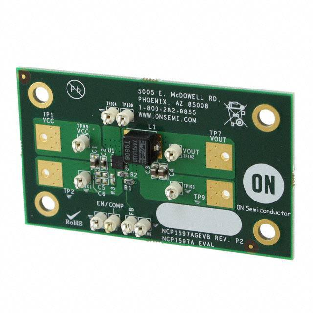
NCP1597AGEVB 是安森美半导体(ON Semiconductor)推出的一款评估板,配套使用的电源管理芯片为 NCP1597A,主要用于评估和开发基于该芯片的 DC/DC 和 AC/DC(离线)开关电源(SMPS)应用。

该评估板主要适用于以下应用场景:

1. 电源适配器:适用于笔记本电脑、工业设备、消费类电子产品的 AC/DC 电源适配器设计评估。

2. 电池充电器:支持用于多节锂电池充电的高效电源拓扑设计,适用于便携设备和工业电池管理系统。

3. 工业电源系统:适合用于工业自动化设备、通信设备、服务器电源等对效率和稳定性要求较高的场景。

4. LED 照明电源:可评估用于高亮度 LED 驱动的恒流/恒压电源设计。

5. 反激式和升压式变换器开发:NCP1597A 支持多种拓扑结构,评估板可帮助工程师快速验证反激、升压等电路性能。

该评估板具备完整的保护功能,如过流、过压、欠压保护,适用于开发高可靠性电源系统。同时支持多种输入电压范围,便于在不同地区和应用场景中使用。
| 参数 | 数值 |
| 产品目录 | 编程器,开发系统 |
| 描述 | BOARD EVALUATION NCP1597A |
| 产品分类 | |
| 品牌 | ON Semiconductor |
| 数据手册 | |
| 产品图片 |
|
| 产品型号 | NCP1597AGEVB |
| rohs | 无铅 / 符合限制有害物质指令(RoHS)规范要求 |
| 产品系列 | - |
| 主要用途 | DC/DC,步降 |
| 使用的IC/零件 | NCP1597A |
| 其它名称 | NCP1597AGEVBOS |
| 功率-输出 | - |
| 所含物品 | 板 |
| 板类型 | 完全填充 |
| 标准包装 | 1 |
| 电压-输入 | 4 V ~ 5.5 V |
| 电压-输出 | 最低可调至 0.8V |
| 电流-输出 | 2A |
| 相关产品 | /product-detail/zh/NCP1597AMNTWG/NCP1597AMNTWG-ND/2748349/product-detail/zh/NCP1597BMNTWG/NCP1597BMNTWG-ND/2481971 |
| 稳压器拓扑 | 降压 |
| 设计资源 | |
| 输出和类型 | 1,非隔离 |
| 频率-开关 | 1MHz |


- 商务部:美国ITC正式对集成电路等产品启动337调查
- 曝三星4nm工艺存在良率问题 高通将骁龙8 Gen1或转产台积电
- 太阳诱电将投资9.5亿元在常州建新厂生产MLCC 预计2023年完工
- 英特尔发布欧洲新工厂建设计划 深化IDM 2.0 战略
- 台积电先进制程称霸业界 有大客户加持明年业绩稳了
- 达到5530亿美元!SIA预计今年全球半导体销售额将创下新高
- 英特尔拟将自动驾驶子公司Mobileye上市 估值或超500亿美元
- 三星加码芯片和SET,合并消费电子和移动部门,撤换高东真等 CEO
- 三星电子宣布重大人事变动 还合并消费电子和移动部门
- 海关总署:前11个月进口集成电路产品价值2.52万亿元 增长14.8%


PDF Datasheet 数据手册内容提取
NCP1597A 1 MHz, 2.0 A Synchronous Buck Regulator The NCP1597A family are fixed 1 MHz, high−output−current, synchronous PWM converters that integrate a low−resistance, high−side P−channel MOSFET and a low−side N−channel MOSFET. The NCP1597A utilizes current mode control to provide fast transient http://onsemi.com response and excellent loop stability. It regulates input voltages from 4.0 V to 5.5 V down to an output voltage as low as 0.8 V and is able to MARKING DIAGRAM supply up to 2.0 A. The NCP1597A includes an internally fixed switching frequency 1 1 1597A (pFinSW, s)h, uantddo awnn i nstueprpnlayl scoufrtr−esntta irst troe dliumceitd i ntoru 3s h(cid:2) Acu rmreanxtism. Uumsi.ng the EN DFN6 AYW(cid:2)W(cid:2) CASE 506AH Other features include cycle−by−cycle current limiting, short−circuit protection, power saving mode and thermal shutdown. A = Assembly Location Y = Year Features WW = Work Week • Input Voltage Range: from 4.0 V to 5.5 V (cid:2) = Pb−Free Package • Internal 140 m(cid:3) High−Side Switching P−Channel MOSFET and (Note: Microdot may be in either location) 90 m(cid:3) Low−Side N−Channel MOSFET • PIN CONNECTIONS Fixed 1 MHz Switching Frequency • Cycle−by−Cycle Current Limiting • FB 1 6 EN Overtemperature Protection • Internal Soft−Start GND 2 5 VCC • Start−up with Pre−Biased Output Load • LX 3 4 VCCP Adjustable Output Voltage Down to 0.8 V • Power Saving Mode During Light Load • These are Pb−Free Devices ORDERING INFORMATION Applications • Device Package Shipping† DSP Power • NCP1597AMNTWG DFN6 3000 / Tape & Hard Disk Drivers (Pb−Free) Reel • Computer Peripherals • †For information on tape and reel specifications, Home Audio including part orientation and tape sizes, please • Set−Top Boxes refer to our Tape and Reel Packaging Specifications • Brochure, BRD8011/D. Networking Equipment • LCD TV • Wireless and DSL/Cable Modem • USB Power Devices © Semiconductor Components Industries, LLC, 2013 1 Publication Order Number: April, 2013 − Rev. 3 NCP1597/D
NCP1597A BLOCK DIAGRAM NCP1597A VCCP VCC + CA Power Reset − NC/EN UTVHLDO Hiccup + OSC PMOS Soft−Start M1 − + PWM Control Vref + gm + Logic LX FB − GND Figure 1. Block Diagram PIN DESCRIPTIONS Pin No Symbol Description 1 FB Feedback input pin of the Error Amplifier. Connect a resistor divider from the converter’s output voltage to this pin to set the converter’s output voltage. 2 GND Ground pin. Connect to thermal pad. 3 LX The drains of the internal MOSFETs. The output inductor should be connected to this pin. 4 VCCP Power input for the power stage 5 VCC Input supply pin for internal bias circuitry. A 0.1 (cid:2)F ceramic bypass capacitor is preferred to connect to this pin. 6 EN Logic input to enable the part. Logic high to turn on the part and logic low to shut off the part. EP PAD Exposed pad of the package provides both electrical contact to the ground and good thermal contact to the PCB. This pad must be soldered to the PCB for proper operation. http://onsemi.com 2
NCP1597A APPLICATION CIRCUIT Vin VCCP LX Vout 4.0 V − 5.5 V VCC GND FB NC/EN Figure 2. NCP1597A ABSOLUTE MAXIMUM RATINGS Rating Symbol Value Unit Power Supply Pin (Pin 4, 5) to GND Vin 6.5 V −0.3 (DC) −1.0 (t < 100 ns) LX to GND Vin + 0.7 V Vin + 1.0 (t < 20 ns) −0.7 (DC) −5.0 (t < 100 ns) All other pins 6.0 V −0.3 (DC) −1.0 (t < 100 ns) Operating Temperature Range TA −40 to +85 °C Junction Temperature TJ −40 to +150 °C Storage Temperature Range TS −55 to +150 °C Thermal Resistance Junction−to−Air (Note 1) R(cid:4)JA 68.5 °C/W Stresses exceeding Maximum Ratings may damage the device. Maximum Ratings are stress ratings only. Functional operation above the Recommended Operating Conditions is not implied. Extended exposure to stresses above the Recommended Operating Conditions may affect device reliability. 1. R(cid:4)JA measured on approximately 1x1 inch sq. of 1 oz. Copper. http://onsemi.com 3
NCP1597A ELECTRICAL CHARACTERISTICS (Vin = 4.0 V − 5.5 V, Vout = 1.2 V, TJ = +25°C for typical value; −40°C < TJ < 85°C for min/max values unless noted otherwise) Parameter Symbol Test Conditions Min Typ Max Unit Vin Input Voltage Range Vin 4.0 5.5 V VCC UVLO Threshold 3.2 3.5 3.8 V UVLO Hysteresis 335 mV VCC Quiescent Current IinVCC Vin = 5 V,VFB = 1.5 V, (No Switching) 1.7 2.0 mA VCCP Quiescent Current IinVCCP Vin = 5 V,VFB = 1.5 V, (No Switching) 25 (cid:2)A Vin Shutdown Supply Current (Note 2) IQSHDN EN = 0 V 1.8 3.0 (cid:2)A FEEDBACK VOLTAGE Reference Voltage VFB 0.788 0.800 0.812 V Feedback Input Bias Current IFB VFB = 0.8 V 10 100 nA Feedback Voltage Line Regulation Vin = 4.0 V to 5.5 V 0.06 %/V PWM Maximum Duty Cycle (Regulating) 82 85 % Minimum Controllable ON Time (Note 2) 50 ns PULSE−BY−PULSE CURRENT LIMIT Pulse−by−Pulse Current Limit (Regulation) ILIM 2.7 3.9 4.3 A Pulse−by−Pulse Current Limit (Soft−Start) ILIMSS 4.0 5.3 6.1 A OSCILLATOR Oscillator Frequency FSW 0.87 1.0 1.13 MHz MOSFET High Side MOSFET ON Resistance RRDDSS((oonn)) IDS = 100 mA, VGS = 5 V 140 200 m(cid:3) HHSS High Side MOSFET Leakage (Note 2) VEN = 0 V, VSW = 0 V 10 (cid:2)A Low Side MOSFET ON Resistance RRDDSS((oonn)) IDS = 100 mA, VGS = 5 V 90 125 m(cid:3) LLSS Low Side MOSFET Leakage (Note 2) VEN = 0 V, VSW = 5 V 10 (cid:2)A ENABLE (NCP1597A) EN HI Threshold ENHI 1.4 V EN LO Threshold ENLO 0.4 V EN Hysteresis 200 mV EN Pullup Current 1.4 3.0 (cid:2)A SOFT−START Soft−Start Ramp Time tSS FSW = 1 MHz 1.0 ms Hiccup Timer 2.0 ms THERMAL SHUTDOWN Thermal Shutdown Threshold 185 °C Thermal Shutdown Hysteresis 30 °C 2. Guaranteed by design. Not production tested. http://onsemi.com 4
NCP1597A TYPICAL OPERATING CHARACTERISTICS 3.7 815 V) 3.6 D ( 810 L O 3.5 UVLO Rising Threshold H 805 S E V) R O ( 3.4 TH 800 L T V U U P 3.3 N 795 UVLO Falling Threshold B I F 3.2 , B790 F V 3.1 785 −40 −15 10 35 60 85 −40 −15 10 35 60 85 TA, AMBIENT TEMPERATURE (°C) TA, AMBIENT TEMPERATURE (°C) Figure 3. Undervoltage Lockout vs. Figure 4. Feedback Input Threshold vs. Temperature Temperature 1.3 6.0 z) NCY (MH 11..12 MIT (A) 5.5 ILIM (Soft−Start) E LI 5.0 EQU 1.0 ENT R R H F UR 4.5 C 0.9 C WIT , M , SW 0.8 ILI 4.0 ILIM (Regulation) S f 0.7 3.5 −40 −15 10 35 60 85 −40 −15 10 35 60 85 TA, AMBIENT TEMPERATURE (°C) TA, AMBIENT TEMPERATURE (°C) Figure 5. Switching Frequency vs. Figure 6. Current Limit vs. Temperature Temperature 2.0 2.0 1.8 1.8 mA) A) G( 1.6 (cid:2)D( 1.6 N E HI L WITC 1.4 DISAB 1.4 , SC , CC C I I 1.2 1.2 1.0 1.0 −40 −15 10 35 60 85 −40 −15 10 35 60 85 TA, AMBIENT TEMPERATURE (°C) TA, AMBIENT TEMPERATURE (°C) Figure 7. Quiescent Current Into V vs. CC Figure 8. Quiescent Current Into V vs. CC Temperature Temperature http://onsemi.com 5
NCP1597A TYPICAL OPERATING CHARACTERISTICS 3.40 100 3.38 VOUT = 3.3 V 90 VIN = 4.0 V V) L = 3.3 (cid:2)H GE ( 3.36 COUT = 2 x 22 (cid:2)F 80 VIN = 5.0 V OLTA 33..3324 Y (%) 70 V C T 3.30 N 60 U E UTP 3.28 VIN = 5.0 V FICI 50 O 3.26 EF V, OUT 3.24 VIN = 4.0 V 4300 VL O=U 3T. 3= (cid:2)3H.3 V 3.22 COUT = 2 x 22 (cid:2)F 3.20 20 0 0.2 0.4 0.6 0.8 1.0 1.2 1.4 1.6 1.8 2.0 0.01 0.1 1 10 IOUT, OUTPUT CURRENT (A) IOUT, OUTPUT CURRENT (A) Figure 9. Load Regulation for V = 3.3 V Figure 10. Efficiency vs. Output Current for OUT V = 3.3 V OUT 1.90 100 V) 1.88 VL O=U 3T. 3= (cid:2)1H.8 V 90 VIN = 4.0 V TAGE ( 11..8846 COUT = 2 x 22 (cid:2)F %) 80 VIN = 5.0 V VOL 1.82 VIN = 5.0 V CY ( 70 T 1.80 N 60 U E OUTP 11..7768 VIN = 4.0 V FFICI 50 , UT 1.74 E 40 VOUT = 1.8 V VO L = 3.3 (cid:2)H 1.72 30 COUT = 2 x 22 (cid:2)F 1.70 20 0 0.2 0.4 0.6 0.8 1.0 1.2 1.4 1.6 1.8 2.0 0.01 0.1 1 10 IOUT, OUTPUT CURRENT (A) IOUT, OUTPUT CURRENT (A) Figure 11. Load Regulation for V = 1.8 V Figure 12. Efficiency vs. Output Current for OUT V = 1.8 V OUT 1.30 100 V) 1.28 VL O=U 3T. 3= (cid:2)1H.2 V 90 VIN = 4.0 V E ( 1.26 COUT = 2 x 22 (cid:2)F 80 G TA 1.24 %) VIN = 5.0 V OL 1.22 VIN = 5.0 V Y ( 70 V C T 1.20 N 60 U E UTP 1.18 VIN = 4.0 V FICI 50 , OUT 11..1146 EF 40 VOUT = 1.2 V VO 30 L = 3.3 (cid:2)H 1.12 COUT = 2 x 22 (cid:2)F 1.10 20 0 0.2 0.4 0.6 0.8 1.0 1.2 1.4 1.6 1.8 2.0 0.01 0.1 1 10 IOUT, OUTPUT CURRENT (A) IOUT, OUTPUT CURRENT (A) Figure 13. Load Regulation for V = 1.2 V Figure 14. Efficiency vs. Output Current for OUT V = 1.2 V OUT http://onsemi.com 6
NCP1597A (VIN = 5 V, ILOAD = 100 mA, L = 3.3 (cid:2)H, COUT = 2 x 22 (cid:2)F) (VIN = 5 V, ILOAD = 700 mA, L = 3.3 (cid:2)H, COUT = 2 x 22 (cid:2)F) Upper Trace: LX Pin Switching Waveform, 2 V/div Upper Trace: LX Pin Switching Waveform, 2 V/div Middle Trace: Output Ripple Voltage, 20 mV/div Middle Trace: Output Ripple Voltage, 20 mV/div Lower Trace: Inductor Current, 1 A/div Lower Trace: Inductor Current, 1 A/div Time Scale: 1.0 (cid:2)s/div Time Scale: 1.0 (cid:2)s/div Figure 15. DCM Switching Waveform for Figure 16. CCM Switching Waveform for V = 3.3 V V = 3.3 V OUT OUT (VIN = 5 V, ILOAD = 100 mA, L = 3.3 (cid:2)H, COUT = 2 x 22 (cid:2)F) (VIN = 5 V, ILOAD = 400 mA, L = 3.3 (cid:2)H, COUT = 2 x 22 (cid:2)F) Upper Trace: LX Pin Switching Waveform, 2 V/div Upper Trace: LX Pin Switching Waveform, 2 V/div Middle Trace: Output Ripple Voltage, 20 mV/div Middle Trace: Output Ripple Voltage, 20 mV/div Lower Trace: Inductor Current, 200 mA/div Lower Trace: Inductor Current, 1 A/div Time Scale: 1.0 (cid:2)s/div Time Scale: 1.0 (cid:2)s/div Figure 17. DCM Switching Waveform for Figure 18. CCM Switching Waveform for V = 1.2 V V = 1.2 V OUT OUT (VIN = 5 V, ILOAD = 100 mA, L = 3.3 (cid:2)H, COUT = 2 x 22 (cid:2)F) (VIN = 5 V, ILOAD = 100 mA, L = 3.3 (cid:2)H, COUT = 2 x 22 (cid:2)F) Upper Trace: EN Pin Voltage, 2 V/div Upper Trace: EN Pin Voltage, 2 V/div Middle Trace: Output Voltage, 1 V/div Middle Trace: Output Voltage, 1 V/div Lower Trace: Inductor Current, 100 mA/div Lower Trace: Inductor Current, 100 mA/div Time Scale: 500 (cid:2)s/div Time Scale: 500 (cid:2)s/div Figure 19. Soft−Start Waveforms for V = 3.3 V Figure 20. Soft−Start Waveforms for V = 1.2 V OUT OUT http://onsemi.com 7
NCP1597A (VIN = 5 V, ILOAD = 100 mA, L = 3.3 (cid:2)H, COUT = 2 x 22 (cid:2)F) (VIN = 5 V, ILOAD = 100 mA, L = 3.3 (cid:2)H, COUT = 2 x 22 (cid:2)F) Upper Trace: Output Dynamic Voltage, 100 mV/div Upper Trace: Output Dynamic Voltage, 100 mV/div Lower Trace: Output Current, 500 mA/div Lower Trace: Output Current, 500 mA/div Time Scale: 200 (cid:2)s/div Time Scale: 200 (cid:2)s/div Figure 21. Transient Response for V = Figure 22. Transient Response for V = OUT OUT 3.3 V 3.3 V (VIN = 5 V, ILOAD = 100 mA, L = 3.3 H, COUT = 2 x 22 (cid:2)F) (VIN = 5 V, ILOAD = 100 mA, L = 3.3 H, COUT = 2 x 22 (cid:2)F) Upper Trace: Output Dynamic Voltage, 100 mV/div Upper Trace: Output Dynamic Voltage, 100 mV/div Lower Trace: Output Current, 500 mA/div Lower Trace: Output Current, 500 mA/div Time Scale: 200 (cid:2)s/div Time Scale: 200 (cid:2)s/div Figure 23. Transient Response for V = Figure 24. Transient Response for V = OUT OUT 1.2 V 1.2 V http://onsemi.com 8
NCP1597A DETAILED DESCRIPTION Overview delivering up to 2.0 A of current. When the controller is The NCP1597A is a synchronous PWM controller that disabled or during a Fault condition, the controller’s output incorporates all the control and protection circuitry stage is tri−stated by turning OFF both the upper and lower necessary to satisfy a wide range of applications. The MOSFETs. NCP1597A employs current mode control to provide fast transient response, simple compensation, and excellent Adaptive Dead Time Gate Driver stability. The features of the NCP1597A include a precision In a synchronous buck converter, a certain dead time is reference, fixed 1 MHz switching frequency, a required between the low side drive signal and high side transconductance error amplifier, an integrated high−side drive signal to avoid shoot through. During the dead time, P−channel MOSFET and low−side N−Channel MOSFET, the body diode of the low side FET freewheels the current. internal soft−start, and very low shutdown current. The The body diode has much higher voltage drop than that of protection features of the NCP1597A include internal the MOSFET, which reduces the efficiency significantly. soft−start, pulse−by−pulse current limit, and thermal The longer the body diode conducts, the lower the shutdown. efficiency. In NCP1597A, the drivers and MOSFETs are integrated in a single chip. The parasitic inductance is Reference Voltage minimized. Adaptive dead time control method is used in The NCP1597A incorporates an internal reference that NCP1597A to prevent the shoot through from happening allows output voltages as low as 0.8 V. The tolerance of the and minimizing the diode conduction loss at the same time. internal reference is guaranteed over the entire operating temperature range of the controller. The reference voltage is Pulse Width Modulation trimmed using a test configuration that accounts for error A high−speed PWM comparator, capable of pulse widths amplifier offset and bias currents. as low as 50 ns, is included in the NCP1597A. The inverting input of the comparator is connected to the output of the Oscillator Frequency error amplifier. The non−inverting input is connected to the A fixed precision oscillator is provided. The oscillator the current sense signal. At the beginning of each PWM frequency range is 1 MHz with (cid:2)13% variation. cycle, the CLK signal sets the PWM flip−flop and the upper MOSFET is turned ON. When the current sense signal rises Transconductance Error Amplifier above the error amplifier’s voltage then the comparator will The transconductance error amplifier’s primary function reset the PWM flip−flop and the upper MOSFET will be is to regulate the converter’s output voltage using a resistor turned OFF. divider connected from the converter’s output to the FB pin of the controller, as shown in the applications Schematic. If Power Save Mode a Fault occurs, the amplifier’s output is immediately pulled If the load current decreases, the converter will enter to GND and PWM switching is inhibited. power save mode operation automatically. During power save mode, the converter skips switching and operates with Internal Soft−Start reduced frequency, which minimizes the quiescent current To limit the startup inrush current, an internal soft start and maintain high efficiency. circuit is used to ramp up the reference voltage from 0 V to its final value linearly. The internal soft start time is 1 ms Current Sense typically. The NCP1597A monitors the current in the upper MOSFET. The current signal is required by the PWM Output MOSFETs comparator and the pulse−by−pulse current limiter. The NCP1597A includes low R , both high−side DS(on) P−channel and low−side N−channel MOSFETs capable of http://onsemi.com 9
NCP1597A PROTECTIONS Undervoltage Lockout (UVLO) overcurrent detection while charging the output capacitors. The under voltage lockout feature prevents the controller Hiccup mode reduces input supply current and power from switching when the input voltage is too low to power dissipation during a short circuit. It also allows for much the internal power supplies and reference. Hysteresis must improved system up−time, allowing auto−restart upon be incorporated in the UVLO comparator to prevent IxR removal of a temporary short−circuit. drops in the wiring or PCB traces from causing ON/OFF cycling of the controller during heavy loading at power up Pre−Bias Startup or power down. In some applications the controller will be required to start switching when it’s output capacitors are charged anywhere Overcurrent Protection (OCP) from slightly above 0 V to just below the regulation voltage. NCP1597A detects high side switch current and then This situation occurs for a number of reasons: the compares to a voltage level representing the overcurrent converter’s output capacitors may have residual charge on threshold limit. If the current through the high side FET them or the converter’s output may be held up by a low exceeds the overcurrent threshold limit for seven current standby power supply. NCP1597A supports consecutive switching cycles, overcurrent protection is pre−bias start up by holding Low side FETs off till soft start triggered. ramp reaches the FB Pin voltage. Once the overcurrent protection occurs, hiccup mode engages. First, hiccup mode, turns off both FETs and Thermal Shutdown discharges the internal compensation network at the output The NCP1597A protects itself from over heating with an of the OTA. Next, the IC waits typically 2 ms and then resets internal thermal monitoring circuit. If the junction the overcurrent counter. After this reset, the circuit attempts temperature exceeds the thermal shutdown threshold both another normal soft−start. During soft−start, the overcurrent the upper and lower MOSFETs will be shut OFF. protection threshold is increased to prevent false http://onsemi.com 10
NCP1597A APPLICATION INFORMATION Programming the Output Voltage I ripple The output voltage is set using a resistive voltage divider C (cid:3) (eq. 3) OUT(min) 8(cid:4)f(cid:4)V from the output voltage to FB pin (see Figure 25). So the ripple output voltage is calculated according to Eq.1. Where V is the allowed output voltage ripple. ripple R (cid:5)R The required ESR for this amount of ripple can be Vout(cid:3)VFB(cid:4) 1R 2 (eq. 1) calculated by equation 5. 2 V ripple ESR(cid:3) (eq. 4) Vout I ripple Based on Equation 2 to choose capacitor and check its R1 ESR according to Equation 3. If ESR exceeds the value from Eq.4, multiple capacitors should be used in parallel. Ceramic capacitor can be used in most of the applications. FB In addition, both surface mount tantalum and through−hole aluminum electrolytic capacitors can be used as well. R2 Maximum Output Capacitor NCP1597A family has internal 1 ms fixed soft−start and overcurrent limit. It limits the maximum allowed output Figure 25. Output divider capacitor to startup successfully. The maximum allowed output capacitor can be determined by the equation: Inductor Selection I (cid:7)I (cid:7)(cid:5)ip−p The inductor is the key component in the switching C (cid:3) lim(min) load(max) 2 (eq. 5) regulator. The selection of inductor involves trade−offs out(max) V (cid:9)T out SS(min) among size, cost and efficiency. The inductor value is Where T is the minimum soft−start period (1ms); selected according to the equation 2. SS(min) (cid:6) (cid:8) D is the current ripple. iPP L(cid:3) Vout (cid:4) 1(cid:7) Vout (eq. 2) This is assuming that a constant load is connected. For f(cid:4)I V example, with 3.3 V/2.0 A output and 20% ripple, the max ripple in(max) allowed output capacitors is 546 (cid:2)F. Where V − the output voltage; out f − switching frequency, 1.0 MHz; Input Capacitor Selection Iripple − Ripple current, usually it’s 20% − 30% of output The input capacitor can be calculated by Equation 6. current; 1 Vin(max) − maximum input voltage. Cin(min)(cid:3)Iout(max)(cid:4)Dmax(cid:4)f(cid:4)V (eq. 6) Choose a standard value close to the calculated value to in(ripple) maintain a maximum ripple current within 30% of the Where V is the required input ripple voltage. in(ripple) maximum load current. If the ripple current exceeds this V 30% limit, the next larger value should be selected. Dmax(cid:3) out isthemaximumdutycycle. (eq. 7) The inductor’s RMS current rating must be greater than V in(min) the maximum load current and its saturation current should be about 30% higher. For robust operation in fault conditions Power Dissipation (start−up or short circuit), the saturation current should be The NCP1597A is available in a thermally enhanced high enough. To keep the efficiency high, the series 6−pin, DFN package. When the die temperature reaches resistance (DCR) should be less than 0.1 (cid:3), and the core +185°C, the NCP1597A shuts down (see the material should be intended for high frequency applications. Thermal−Overload Protection section). The power dissipated in the device is the sum of the power dissipated Output Capacitor Selection from supply current (PQ), power dissipated due to switching The output capacitor acts to smooth the dc output voltage the internal power MOSFET (P ), and the power SW and also provides energy storage. So the major parameter dissipated due to the RMS current through the internal necessary to define the output capacitor is the maximum power MOSFET (PON). The total power dissipated in the allowed output voltage ripple of the converter. This ripple is package must be limited so the junction temperature does related to capacitance and the ESR. The minimum not exceed its absolute maximum rating of +150°C at capacitance required for a certain output ripple can be calculated by Equation 4. http://onsemi.com 11
NCP1597A (cid:6) (cid:8) maximum ambient temperature. Calculate the power lost in T (cid:3)T (cid:5) P (cid:4)(cid:4) (eq. 15) J C TOTAL JC the NCP1597A using the following equations: (cid:4) is the junction−to−case thermal resistance equal to 1. High side MOSFET JC 1.7°C/W. T is the temperature of the case and TJ is the C The conduction loss in the top switch is: junction temperature, or die temperature. The P (cid:3)I2 (cid:10)R (eq. 8) case−to−ambient thermal resistance is dependent on how HSON RMS_HSFET DS(on)HS well heat can be transferred from the PC board to the air. Where: (cid:11) Solder the underside−exposed pad to a large copper GND (cid:6) (cid:8) (cid:5)I 2 plane. If the die temperature reaches the thermal shutdown I (cid:3) I 2(cid:5) PP (cid:10)D (eq. 9) threshold the NCP1597A shut down and does not restart RMS_FET out 12 again until the die temperature cools by 30°C. (cid:5)IPP is the peak−to−peak inductor current ripple. Layout Consideration The power lost due to switching the internal power high side As with all high frequency switchers, when considering MOSFET is: layout, care must be taken in order to achieve optimal (cid:6) (cid:8) electrical, thermal and noise performance. For 1.0MHz P (cid:3)Vin(cid:4)Iout(cid:4) tr(cid:5)tf (cid:4)fSW (eq. 10) switching frequency, switch rise and fall times are typically HSSW 2 in few nanosecond range. To prevent noise both radiated and conducted the high speed switching current path must be tr and tf are the rise and fall times of the internal power kept as short as possible. Shortening the current path will MOSFET measured at SW node. also reduce the parasitic trace inductance of approximately 2. Low side MOSFET 25 nH/inch. At switch off, this parasitic inductance The power dissipated in the top switch is: produces a flyback spike across the NCP1597A switch. P (cid:3)I 2(cid:4)R (eq. 11) When operating at higher currents and input voltages, with LSON RMS_LSFET DS(on)LS poor layout, this spike can generate voltages across the Where: NCP1597A that may exceed its absolute maximum rating. (cid:11) (cid:6) (cid:8) A ground plane should always be used under the switcher (cid:5)I 2 IRMS_LSFET(cid:3) Iout2(cid:5) 1P2P (cid:4)(1(cid:7)D) (eq. 12) cirTcuhiet rFyB t oc opmrepvoennet nitn stehropulladn eb ec okeupptl iansg f aarn daw oavye raasl lp noossiisbel.e from the switch node. The ground for these components (cid:5)I is the peak−to−peak inductor current ripple. PP should be separated from the switch current path. Failure to The switching loss for the low side MOSFET can be do so will result in poor stability or subharmonic like ignored. oscillation. The power lost due to the quiescent current (I ) of the device Board layout also has a significant effect on thermal Q is: resistance. Reducing the thermal resistance from ground pin and exposed pad onto the board will reduce die temperature P (cid:3)V (cid:4)I (eq. 13) Q in Q and increase the power capability of the NCP1597A. This is IQ is the switching quiescent current of the NCP1597A. achieved by providing as much copper area as possible P (cid:3)P (cid:5)P (cid:5)P (cid:5)P (eq. 14) around the exposed pad. Adding multiple thermal vias under TOTAL HSON HSSW LSON Q and around this pad to an internal ground plane will also Calculate the temperature rise of the die using the following help. Similar treatment to the inductor pads will reduce any equation: additional heating effects. http://onsemi.com 12
NCP1597A PACKAGE DIMENSIONS DFN6 3x3, 0.95P CASE 506AH ISSUE O D A NOTES: B 1. DIMENSIONS AND TOLERANCING PER ASME Y14.5M, 1994. 2. CONTROLLING DIMENSION: MILLIMETERS. 3. DIMESNION b APPLIES TO PLATED TERMINAL AND IS MEASURED BETWEEN 0.25 AND 0.30 PIN 1 MM FROM TERMINAL. REFERENCE ÇÇÇ 4. COPLANARITY APPLIES TO THE EXPOSED E PAD AS WELL AS THE TERMINALS. ÇÇÇ MILLIMETERS 2X ÇÇÇ DIM MIN NOM MAX 0.15 C A 0.80 0.90 1.00 ÇÇÇ A1 0.00 0.03 0.05 2X A3 0.20 REF 0.15 C b 0.35 0.40 0.45 TOP VIEW D 3.00 BSC D2 2.40 2.50 2.60 0.10 C E 3.00 BSC E2 1.50 1.60 1.70 A e 0.95 BSC 6X K 0.21 −−− −−− 0.08 C SEATING L 0.30 0.40 0.50 (A3) PLANE SIDE VIEW A1 C SOLDERING FOOTPRINT* D2 6XL e 4X 00..0415707 0.950 1 3 0.0374 E2 6X K 3.31 1.700 6 4 0.130 0.685 6X b (NOTE 3) 0.10 C A B 0.05 C BOTTOM VIEW 2.60 0.63 0.025 0.1023 (cid:6) (cid:8) mm SCALE 10:1 inches *For additional information on our Pb−Free strategy and soldering details, please download the ON Semiconductor Soldering and Mounting Techniques Reference Manual, SOLDERRM/D. ON Semiconductor and are registered trademarks of Semiconductor Components Industries, LLC (SCILLC). SCILLC reserves the right to make changes without further notice to any products herein. SCILLC makes no warranty, representation or guarantee regarding the suitability of its products for any particular purpose, nor does SCILLC assume any liability arising out of the application or use of any product or circuit, and specifically disclaims any and all liability, including without limitation special, consequential or incidental damages. “Typical” parameters which may be provided in SCILLC data sheets and/or specifications can and do vary in different applications and actual performance may vary over time. All operating parameters, including “Typicals” must be validated for each customer application by customer’s technical experts. SCILLC does not convey any license under its patent rights nor the rights of others. SCILLC products are not designed, intended, or authorized for use as components in systems intended for surgical implant into the body, or other applications intended to support or sustain life, or for any other application in which the failure of the SCILLC product could create a situation where personal injury or death may occur. Should Buyer purchase or use SCILLC products for any such unintended or unauthorized application, Buyer shall indemnify and hold SCILLC and its officers, employees, subsidiaries, affiliates, and distributors harmless against all claims, costs, damages, and expenses, and reasonable attorney fees arising out of, directly or indirectly, any claim of personal injury or death associated with such unintended or unauthorized use, even if such claim alleges that SCILLC was negligent regarding the design or manufacture of the part. SCILLC is an Equal Opportunity/Affirmative Action Employer. This literature is subject to all applicable copyright laws and is not for resale in any manner. PUBLICATION ORDERING INFORMATION LITERATURE FULFILLMENT: N. American Technical Support: 800−282−9855 Toll Free ON Semiconductor Website: www.onsemi.com Literature Distribution Center for ON Semiconductor USA/Canada P.O. Box 5163, Denver, Colorado 80217 USA Europe, Middle East and Africa Technical Support: Order Literature: http://www.onsemi.com/orderlit Phone: 303−675−2175 or 800−344−3860 Toll Free USA/Canada Phone: 421 33 790 2910 Fax: 303−675−2176 or 800−344−3867 Toll Free USA/Canada Japan Customer Focus Center For additional information, please contact your local Email: orderlit@onsemi.com Phone: 81−3−5817−1050 Sales Representative http://onsemi.com NCP1597/D 13