ICGOO在线商城 > 集成电路(IC) > 逻辑 - 栅极和逆变器 > NC7SVL04L6X
 Datasheet下载
- 型号: NC7SVL04L6X
- 制造商: Fairchild Semiconductor
- 库位|库存: xxxx|xxxx
- 要求:
| 数量阶梯 | 香港交货 | 国内含税 |
| +xxxx | $xxxx | ¥xxxx |
查看当月历史价格
查看今年历史价格
NC7SVL04L6X产品简介:
ICGOO电子元器件商城为您提供NC7SVL04L6X由Fairchild Semiconductor设计生产,在icgoo商城现货销售,并且可以通过原厂、代理商等渠道进行代购。 NC7SVL04L6X价格参考。Fairchild SemiconductorNC7SVL04L6X封装/规格:逻辑 - 栅极和逆变器, 反相器 IC 1 Channel 6-MicroPak。您可以下载NC7SVL04L6X参考资料、Datasheet数据手册功能说明书,资料中有NC7SVL04L6X 详细功能的应用电路图电压和使用方法及教程。
ON Semiconductor(安森美)的NC7SVL04L6X是一款超低电压、单通道反相器(逆变器),属于逻辑 - 栅极和逆变器类别。该器件采用先进的CMOS技术,工作电压范围宽(1.65V至3.6V),功耗低,适合电池供电或对能效要求较高的便携式设备。

其主要应用场景包括:

1. 移动通信设备:广泛用于智能手机、平板电脑中的信号电平转换与逻辑控制,支持低电压系统间的接口匹配。
2. 消费类电子产品:如可穿戴设备、智能手表、无线耳机等,利用其小封装(SOT-363/SC-88)和低静态电流特性,节省空间并延长电池寿命。
3. 工业控制与传感器模块:在微控制器(MCU)与外围传感器、执行器之间实现信号整形与驱动,提升系统稳定性。
4. 电源管理电路:用于使能信号反相、复位电路设计等,确保数字系统的时序正确性。
5. 物联网(IoT)终端设备:适用于各类无线模块(如Wi-Fi、蓝牙、ZigBee)中的逻辑电平处理,满足小型化和低功耗需求。

NC7SVL04L6X具备高噪声抑制能力和快速响应时间,能够在复杂电磁环境中稳定运行,是现代低功耗数字系统中理想的逻辑反相解决方案。
| 参数 | 数值 |
| 产品目录 | 集成电路 (IC) |
| 描述 | IC INVERTER SGL 6-MICROPAK |
| 产品分类 | |
| 品牌 | Fairchild Semiconductor |
| 数据手册 | |
| 产品图片 |
|
| 产品型号 | NC7SVL04L6X |
| PCN设计/规格 | |
| rohs | 无铅 / 符合限制有害物质指令(RoHS)规范要求 |
| 产品系列 | 7SVL |
| 不同V、最大CL时的最大传播延迟 | 3.5ns @ 3V, 30pF |
| 产品目录页面 | |
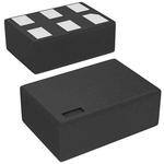
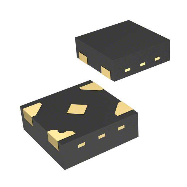
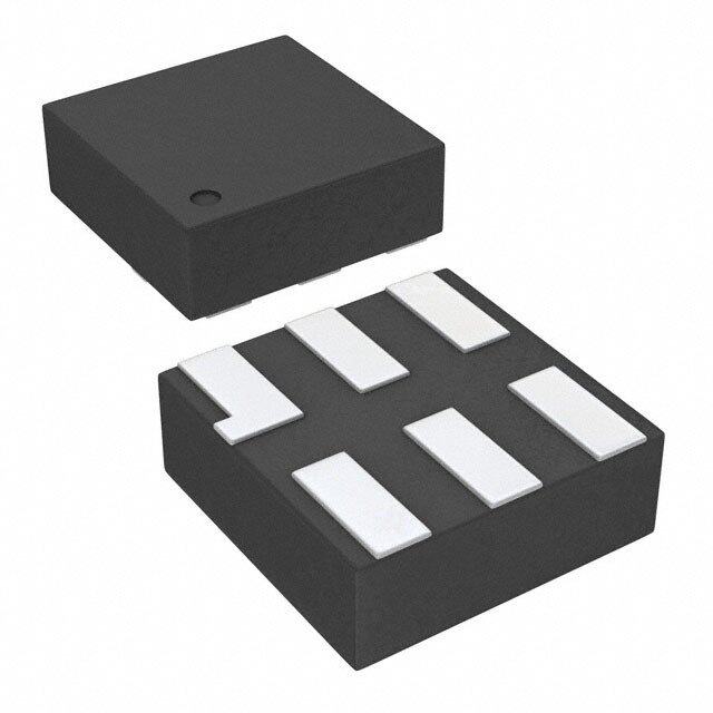
| 供应商器件封装 | 6-MicroPak |
| 其它名称 | NC7SVL04L6XDKR |
| 包装 | Digi-Reel® |
| 安装类型 | 表面贴装 |
| 封装/外壳 | 6-UFDFN |
| 工作温度 | -40°C ~ 85°C |
| 标准包装 | 1 |
| 特性 | - |
| 电压-电源 | 0.9 V ~ 3.6 V |
| 电流-输出高,低 | 24mA,24mA |
| 电流-静态(最大值) | 0.9µA |
| 电路数 | 1 |
| 输入数 | 1 |
| 逻辑电平-低 | 0.7 V ~ 0.8 V |
| 逻辑电平-高 | 0.9 V ~ 1.5 V |
| 逻辑类型 |


PDF Datasheet 数据手册内容提取
Is Now Part of To learn more about ON Semiconductor, please visit our website at www.onsemi.com Please note: As part of the Fairchild Semiconductor integration, some of the Fairchild orderable part numbers will need to change in order to meet ON Semiconductor’s system requirements. Since the ON Semiconductor product management systems do not have the ability to manage part nomenclature that utilizes an underscore (_), the underscore (_) in the Fairchild part numbers will be changed to a dash (-). This document may contain device numbers with an underscore (_). Please check the ON Semiconductor website to verify the updated device numbers. The most current and up-to-date ordering information can be found at www.onsemi.com. Please email any questions regarding the system integration to Fairchild_questions@onsemi.com. ON Semiconductor and the ON Semiconductor logo are trademarks of Semiconductor Components Industries, LLC dba ON Semiconductor or its subsidiaries in the United States and/or other countries. ON Semiconductor owns the rights to a number of patents, trademarks, copyrights, trade secrets, and other intellectual property. A listing of ON Semiconductor’s product/patent coverage may be accessed at www.onsemi.com/site/pdf/Patent-Marking.pdf. ON Semiconductor reserves the right to make changes without further notice to any products herein. ON Semiconductor makes no warranty, representation or guarantee regarding the suitability of its products for any particular purpose, nor does ON Semiconductor assume any liability arising out of the application or use of any product or circuit, and specifically disclaims any and all liability, including without limitation special, consequential or incidental damages. Buyer is responsible for its products and applications using ON Semiconductor products, including compliance with all laws, regulations and safety requirements or standards, regardless of any support or applications information provided by ON Semiconductor. “Typical” parameters which may be provided in ON Semiconductor data sheets and/or specifications can and do vary in different applications and actual performance may vary over time. All operating parameters, including “Typicals” must be validated for each customer application by customer’s technical experts. ON Semiconductor does not convey any license under its patent rights nor the rights of others. ON Semiconductor products are not designed, intended, or authorized for use as a critical component in life support systems or any FDA Class 3 medical devices or medical devices with a same or similar classification in a foreign jurisdiction or any devices intended for implantation in the human body. Should Buyer purchase or use ON Semiconductor products for any such unintended or unauthorized application, Buyer shall indemnify and hold ON Semiconductor and its officers, employees, subsidiaries, affiliates, and distributors harmless against all claims, costs, damages, and expenses, and reasonable attorney fees arising out of, directly or indirectly, any claim of personal injury or death associated with such unintended or unauthorized use, even if such claim alleges that ON Semiconductor was negligent regarding the design or manufacture of the part. ON Semiconductor is an Equal Opportunity/Affirmative Action Employer. This literature is subject to all applicable copyright laws and is not for resale in any manner.
N C 7 S V November 2010 L 0 4 — T i n y NC7SVL04 L o ® g TinyLogic Low-I Inverter i CCT c ® L o w - Features Description CI C T (cid:131) 0.9V to 3.6V VCC Supply Operation The NC7SVL04 is a single inverter with a low-ICCT input In design from Fairchild’s Ultra-Low Power (ULP-A) series v (cid:131) 3.6V Over-Voltage Tolerant I/Os at VCC from 0.9V of TinyLogic®. The NC7SVL04 features very low e r to 3.6V quiescent current, even when the input voltage is lower t e (cid:131) Power-Off High Impedance Inputs and Outputs than the VCC supply. This feature services mobile r handset applications very well, allowing for direct (cid:131) Proprietary Quiet Series™ Noise / EMI Reduction interface with baseband processor general-purpose Circuitry I/Os. Since mobile devices rely on a battery supply, the (cid:131) Ultra-Small MicroPak™ Package NC7SVL04 facilitates lower power consumption in mixed-voltage rail environments. (cid:131) Ultra-Low Dynamic Power This product is designed on an advanced CMOS technology for a wide low-voltage operating range (0.9V to 3.6V V ), high drive needs (up to 24mA), and speed CC (maximum propagation delay of 3.5ns, V =3.3V). It CC achieves this performance while maintaining low CMOS power dissipation. Ordering Information Part Number Top Mark Package Packing Method 3000 Units on NC7SVL04P5X L04 5-Lead SC70, EIAJ SC-88a, 1.25mm Wide Tape & Reel 5000 Units on NC7SVL04L6X CD 6-Lead MicroPak™, 1.00mm Wide Tape & Reel 5000 Units on NC7SVL04FHX CD 6-Lead, MicroPak2™, 1x1mm Body, .35mm Pitch Tape & Reel © 2008 Fairchild Semiconductor Corporation www.fairchildsemi.com NC7SVL04 • Rev. 1.0.4
N C 7 Connection Diagram S V L IEEE/IEC 0 4 — T i n y L o Figure 1. Logic Symbol g i c ® L o w Pin Configurations I C C T I n v e r t e r Figure 2. SC70 (Top View) Figure 3. MicroPak™ (Top Through View) Pin Definitions Pin # SC70 Pin # MicroPak™ Name Description 1 1 NC No Connect 2 2 A Input 3 3 GND Ground 4 4 Y Output 5 6 V Supply Voltage CC 5 NC No Connect Function Table Y=/A Inputs Output A Y L H H L H = HIGH Logic Level L = LOW Logic Level © 2008 Fairchild Semiconductor Corporation www.fairchildsemi.com NC7SVL04 • Rev. 1.0.4 2
N Absolute Maximum Ratings C 7 Stresses exceeding the absolute maximum ratings may damage the device. The device may not function or be S V operable above the recommended operating conditions and stressing the parts to these levels is not recommended. L In addition, extended exposure to stresses above the recommended operating conditions may affect device 0 4 reliability. The absolute maximum ratings are stress ratings only. — Symbol Parameter Min. Max. Unit T i V Supply Voltage -0.5 4.6 V n CC y V DC Input Voltage -0.5 4.6 V L IN o HIGH or LOW State(1) -0.5 V + 0.5 g VOUT DC Output Voltage CC V ic VCC=0V -0.5 4.6 ® L IIK DC Input Diode Current VIN < 0V -50 mA o w V < 0V -50 IOK DC Output Diode Current OUT mA C I VOUT > VCC +50 C T IOH / IOL DC Output Source/Sink Current ±50 mA In I or I DC V or Ground Current per Supply Pin ±50 mA v CC GND CC e r TSTG Storage Temperature Range -65 +150 °C te r TJ Junction Temperature Under Bias +150 °C T Junction Lead Temperature, Soldering 10 Seconds +260 °C L SC70-5 150 P Power Dissipation at +85°C MicroPak™-6 130 mW D MicroPak2™-6 120 Human Body Model, JEDEC:JESD22-A114 4000 ESD V Charge Device Model, JEDEC:JESD22-C101 2000 Note: 1. I absolute maximum ratings must be observed. O Recommended Operating Conditions The Recommended Operating Conditions table defines the conditions for actual device operation. Recommended operating conditions are specified to ensure optimal performance to the datasheet specifications. Fairchild does not recommend exceeding them or designing to Absolute Maximum Ratings. Symbol Parameter Conditions Min. Max. Unit V Supply Voltage 0.9 3.6 V CC V Input Voltage 0 3.6 V IN V =0V 0 3.6 CC V Output Voltage V OUT HIGH or LOW State 0 V CC V =3.0V to 3.6V ±24.0 CC V =2.3V to 2.7V ±18.0 CC V =1.65V to 1.95V ±6.0 CC I /I Output Current in I /I mA OH OL OH OL V =1.4V to 1.6V ±4.0 CC V =1.1V to 1.3V ±2.0 CC V =0.9V ±0.1 CC T Operating Temperature, Free Air -40 +85 °C A Δt/ΔV Minimum Input Edge Rate VIN=0.8V to 2.0V, VCC=3.0V 10 ns/V SC70-5 425 θ Thermal Resistance MicroPak™-6 500 °C/W JA MicroPak2™-6 560 Note: 2. Unused inputs must be held HIGH or LOW. They may not float. © 2008 Fairchild Semiconductor Corporation www.fairchildsemi.com NC7SVL04 • Rev. 1.0.4 3
N C DC Electrical Characteristics 7 S V T =25°C T =-40 to +85°C Symbol Parameter V Conditions A A Units L CC 0 Min. Max. Min. Max. 4 0.90 .65 x VCC .65 x VCC — 1.10 ≤ VCC ≤ 1.30 .65 x VCC .65 x VCC T i n HIGH Level Input 1.40 ≤ VCC ≤ 1.60 .65 x VCC .65 x VCC y VIH Voltage 1.65 ≤ VCC ≤ 1.95 0.90 .0.90 V Lo g 2.30 ≤ VCC ≤ 2.70 1.50 1.50 i c 2.70 ≤ VCC ≤ 3.60 1.50 1.50 ® L 0.90 .25 x VCC .25 x VCC o w 1.10 ≤ VCC ≤ 1.30 .25 x VCC .25 x VCC I C LOW Level Input 1.40 ≤ VCC ≤ 1.60 .25 x VCC .25 x VCC C VIL Voltage 1.65 ≤ VCC ≤ 1.95 .25 x VCC .25 x VCC V T In 2.30 ≤ VCC ≤ 2.70 0.70 0.70 ve 2.70 ≤ VCC ≤ 3.60 0.80 0.80 rte 0.90 VCC-0.10 VCC-0.10 r 1.10 ≤ VCC ≤ 1.30 VCC-0.10 VCC-0.10 1.40 ≤ VCC ≤ 1.60 VCC-0.20 VCC-0.20 IOH=-100µA 1.65 ≤ VCC ≤ 1.95 VCC-0.20 VCC-0.20 2.30 ≤ VCC ≤ 2.70 VCC-0.20 VCC-0.20 2.70 ≤ VCC ≤ 3.60 VCC-0.20 VCC-0.20 1.10 ≤ VCC ≤ 1.30 IOH=-2mA .75 x VCC .75 x VCC HIGH Level Output VOH Voltage 1.40 ≤ VCC ≤ 1.60 IOH=-4mA .75 x VCC .75 x VCC V 1.65 ≤ VCC ≤ 1.95 1.25 1.25 IOH=-6mA 2.30 ≤ VCC ≤ 2.70 2.00 2.00 2.30 ≤ VCC ≤ 2.70 1.80 1.80 IOH=-12mA 2.70≤ VCC ≤ 3.60 2.20 2.20 2.30 ≤ VCC ≤ 2.70 1.70 1.70 IOH=-18mA 2.70 ≤ VCC ≤ 3.60 2.40 2.40 2.70 ≤ VCC ≤ 3.60 IOH=-24mA 2.20 2.20 Continued on the following page… © 2008 Fairchild Semiconductor Corporation www.fairchildsemi.com NC7SVL04 • Rev. 1.0.4 4
N C DC Electrical Characteristics (Continued) 7 S V T =25°C T =-40 to 85°C Symbol Parameter V Conditions A A Units L CC 0 Min. Max. Min. Max. 4 0.90 0.10 0.10 — 1.10 ≤ VCC ≤ 1.30 0.10 0.10 T i n 1.40 ≤ VCC ≤ 1.60 0.20 0.20 y IOL=100µA L 1.65 ≤ VCC ≤ 1.95 0.20 0.20 o g 2.30 ≤ VCC ≤ 2.70 0.20 0.20 i c 2.70 ≤ VCC ≤ 3.60 0.20 0.20 ® L LOW Level 1.10 ≤ VCC ≤ 1.30 IOL=2mA 0.25 x VCC 0.25 x VCC o VOL Output Voltage 1.40 ≤ VCC ≤ 1.60 IOL=4mA 0.25 x VCC 0.25 x VCC V w I 1.65 ≤ VCC ≤ 1.95 IOL=6mA 0.30 0.30 CC T 22..3700 ≤≤ VVCCCC ≤≤ 23..7600 IOL=12mA 00..4400 00..4400 Inve 22..3700 ≤≤ VVCCCC ≤≤ 23..7600 IOL=18mA 00..6400 00..6400 rter 2.70 ≤ VCC ≤ 3.60 IOL=24mA 0.55 0.55 Input Leakage IIN Current 0.90 to 3.60 0 ≤ VIN ≤ 3.60V ±0.1 ±0.5 µA Power Off IOFF Leakage 0 0 ≤ (VIN, VO) ≤ 3.60V 0.5 0.5 µA Current Quiescent VIN=VCC or GND 0.9 0.9 ICC Supply Current 0.90 to 3.60 VCC ≤ VIN ≤ 3.60V ±0.9 µA ICCT Ipnecrr eInapsuet in ICC 13..9650 VVIINN==01..95VV 66 88 µA AC Electrical Characteristics T =25°C T =-40 to 85°C A A Symbol Parameter V Conditions Units Figure CC Min. Typ. Max. Min. Max. 0.90 CL=15pF, RL=1MΩ 34.0 1.10 ≤ VCC ≤ 1.30 3.5 8.1 16.5 3.0 27.8 CL=15pF, RL=2kΩ Propagation 1.40 ≤ VCC ≤ 1.60 1.5 3.7 7.0 1.5 7.5 Figure 4 tPHL, tPLH Delay 1.65 ≤ VCC ≤ 1.95 1.1 2.8 5.8 1.0 6.3 ns Figure 5 2.30 ≤ VCC ≤ 2.70 CRLL==53000pΩF, 0.6 2.0 4.0 0.6 4.5 2.70 ≤ VCC ≤ 3.60 0.5 1.5 3.5 0.5 4.0 Input CIN Capacitance 0 3 pF Power CPD Dissipation 0.90 to 3.60 fV=IN1=00MVH ozr VCC, 5 pF Capacitance © 2008 Fairchild Semiconductor Corporation www.fairchildsemi.com NC7SVL04 • Rev. 1.0.4 5
N C AC Loadings and Waveforms 7 S V L 0 4 — T i n y L o g i c ® L o w I C C Figure 4. AC Test Circuit T I n v e r t e r Figure 5. AC Waveforms V CC Symbol 3.3V ± 0.3V 2.5V ± 0.2V 1.8V ± 0.15V 1.5V ± 0.1V 1.2V ± 0.1V 0.9V V 1.5V V /2 V /2 V /2 V /2 V /2 mi CC CC CC CC CC V 1.5V V /2 V /2 V /2 V /2 V /2 mo CC CC CC CC CC © 2008 Fairchild Semiconductor Corporation www.fairchildsemi.com NC7SVL04 • Rev. 1.0.4 6
N C Physical Dimensions 7 S V L 0 4 — T i n y L o g i c ® L o w I C C T I n v e r t e r Figure 6. 5-Lead, SC70, EIAJ SC-88a, 1.25mm Wide Package drawings are provided as a service to customers considering Fairchild components. Drawings may change in any manner without notice. Please note the revision and/or date on the drawing and contact a Fairchild Semiconductor representative to verify or obtain the most recent revision. Package specifications do not expand the terms of Fairchild’s worldwide terms and conditions, specifically the warranty therein, which covers Fairchild products. Always visit Fairchild Semiconductor’s online packaging area for the most recent package drawings: http://www.fairchildsemi.com/packaging/. Tape and Reel Specifications Please visit Fairchild Semiconductor’s online packaging area for the most recent tape and reel specifications: http://www.fairchildsemi.com/products/analog/pdf/sc70-5_tr.pdf. Package Designator Tape Section Cavity Number Cavity Status Cover Type Status Leader (Start End) 125 (Typical) Empty Sealed P5X Carrier 3000 Filled Sealed Trailer (Hub End) 75 (Typical) Empty Sealed © 2008 Fairchild Semiconductor Corporation www.fairchildsemi.com NC7SVL04 • Rev. 1.0.4 7
N C 7 Physical Dimensions S V L 2X 0 4 0.05 C 1.45 B 2X (1) — 0.05 C T i n y L (0.254) 1.00 (0.49) o 5X g i (0.75) c ® L (0.52) o PIN 1 IDENTIFIER TOP VIEW A 1X w 5 CI 0.55MAX (0.30) C T PIN 1 6X I 0.05 C n v 0.05 RECOMMENED e 0.00 r LAND PATTERN t e 0.05 C r C 0.45 0.106X 0.35 0.25 0.00 6X 0.15 DETAIL A 1.0 0.10 C B A 0.05 C 0.40 0.30 0.35 5X 0.25 00..4300 5X DETAIL A 0.075 X 45 PIN 1 TERMINAL (0.05) 0.5 CHAMFER (0.13) 6X 4X BOTTOM VIEW Notes: 1. CONFORMS TO JEDEC STANDARD M0-252 VARIATION UAAD 2. DIMENSIONS ARE IN MILLIMETERS 3. DRAWING CONFORMS TO ASME Y14.5M-1994 4. FILENAME AND REVISION: MAC06AREV4 5. PIN ONE IDENTIFIER IS 2X LENGTH OF ANY OTHER LINE IN THE MARK CODE LAYOUT. Figure 7. 6-Lead, MicroPak™, 1.0mm Wide Package drawings are provided as a service to customers considering Fairchild components. Drawings may change in any manner without notice. Please note the revision and/or date on the drawing and contact a Fairchild Semiconductor representative to verify or obtain the most recent revision. Package specifications do not expand the terms of Fairchild’s worldwide terms and conditions, specifically the warranty therein, which covers Fairchild products. Always visit Fairchild Semiconductor’s online packaging area for the most recent package drawings: http://www.fairchildsemi.com/packaging/. Tape and Reel Specifications Please visit Fairchild Semiconductor’s online packaging area for the most recent tape and reel specifications: http://www.fairchildsemi.com/products/logic/pdf/micropak_tr.pdf. Package Designator Tape Section Cavity Number Cavity Status Cover Type Status Leader (Start End) 125 (Typical) Empty Sealed L6X Carrier 5000 Filled Sealed Trailer (Hub End) 75 (Typical) Empty Sealed © 2008 Fairchild Semiconductor Corporation www.fairchildsemi.com NC7SVL04 • Rev. 1.0.4 8
N C Physical Dimensions 7 S V 0.89 L 0.05 C 0.35 04 2X 1.00 B A — 5X 0.40 T i PIN 1 n 0.66 y MIN 250uM L 1.00 o 1X 0.45 g i c ® 6X 0.19 L 0.05 C o TOP VIEW 2X RECOMMENDED LAND PATTERN w FOR SPACE CONSTRAINED PCB I C 0.90 C T 0.05 C 0.35 I n v e C 0.55MAX 5X0.52 rt e r SIDE VIEW 0.73 (0.08) 4X 0.09 1X0.57 DETAIL A 1 2 3 0.19 6X 0.20 6X ALTERNATIVE LAND PATTERN FOR UNIVERSAL APPLICATION (0.05) 6X 5X 0.35 0.25 0.60 6 5 4 0.10 C B A 0.35 0.40 (0.08) .05 C 0.30 4X BOTTOM VIEW NOTES: A. COMPLIES TO JEDEC MO-252 STANDARD B. DIMENSIONS ARE IN MILLIMETERS. C. DIMENSIONS AND TOLERANCES PER ASME Y14.5M, 1994 0.075X45° D. LANDPATTERN RECOMMENDATION IS BASED ON FSC CHAMFER DETAIL A DESIGN. PIN 1 LEAD SCALE: 2X E. DRAWING FILENAME AND REVISION: MGF06AREV3 Figure 8. 6-Lead, MicroPak2™, 1x1mm Body, .35mm Pitch Package drawings are provided as a service to customers considering Fairchild components. Drawings may change in any manner without notice. Please note the revision and/or date on the drawing and contact a Fairchild Semiconductor representative to verify or obtain the most recent revision. Package specifications do not expand the terms of Fairchild’s worldwide terms and conditions, specifically the warranty therein, which covers Fairchild products. Always visit Fairchild Semiconductor’s online packaging area for the most recent package drawings: http://www.fairchildsemi.com/packaging/. Tape and Reel Specifications Please visit Fairchild Semiconductor’s online packaging area for the most recent tape and reel specifications: http://www.fairchildsemi.com/packaging/MicroPAK2_6L_tr.pdf. Package Designator Tape Section Cavity Number Cavity Status Cover Type Status Leader (Start End) 125 (Typical) Empty Sealed FHX Carrier 5000 Filled Sealed Trailer (Hub End) 75 (Typical) Empty Sealed © 2008 Fairchild Semiconductor Corporation www.fairchildsemi.com NC7SVL04 • Rev. 1.0.4 9
N C 7 S V L 0 4 — T i n y L o g i c ® L o w I C C T I n v e r t e r © 2008 Fairchild Semiconductor Corporation www.fairchildsemi.com NC7SVL04 • Rev. 1.0.4 10
ON Semiconductor and are trademarks of Semiconductor Components Industries, LLC dba ON Semiconductor or its subsidiaries in the United States and/or other countries. ON Semiconductor owns the rights to a number of patents, trademarks, copyrights, trade secrets, and other intellectual property. A listing of ON Semiconductor’s product/patent coverage may be accessed at www.onsemi.com/site/pdf/Patent−Marking.pdf. ON Semiconductor reserves the right to make changes without further notice to any products herein. ON Semiconductor makes no warranty, representation or guarantee regarding the suitability of its products for any particular purpose, nor does ON Semiconductor assume any liability arising out of the application or use of any product or circuit, and specifically disclaims any and all liability, including without limitation special, consequential or incidental damages. Buyer is responsible for its products and applications using ON Semiconductor products, including compliance with all laws, regulations and safety requirements or standards, regardless of any support or applications information provided by ON Semiconductor. “Typical” parameters which may be provided in ON Semiconductor data sheets and/or specifications can and do vary in different applications and actual performance may vary over time. All operating parameters, including “Typicals” must be validated for each customer application by customer’s technical experts. ON Semiconductor does not convey any license under its patent rights nor the rights of others. ON Semiconductor products are not designed, intended, or authorized for use as a critical component in life support systems or any FDA Class 3 medical devices or medical devices with a same or similar classification in a foreign jurisdiction or any devices intended for implantation in the human body. Should Buyer purchase or use ON Semiconductor products for any such unintended or unauthorized application, Buyer shall indemnify and hold ON Semiconductor and its officers, employees, subsidiaries, affiliates, and distributors harmless against all claims, costs, damages, and expenses, and reasonable attorney fees arising out of, directly or indirectly, any claim of personal injury or death associated with such unintended or unauthorized use, even if such claim alleges that ON Semiconductor was negligent regarding the design or manufacture of the part. ON Semiconductor is an Equal Opportunity/Affirmative Action Employer. This literature is subject to all applicable copyright laws and is not for resale in any manner. PUBLICATION ORDERING INFORMATION LITERATURE FULFILLMENT: N. American Technical Support: 800−282−9855 Toll Free ON Semiconductor Website: www.onsemi.com Literature Distribution Center for ON Semiconductor USA/Canada 19521 E. 32nd Pkwy, Aurora, Colorado 80011 USA Europe, Middle East and Africa Technical Support: Order Literature: http://www.onsemi.com/orderlit Phone: 303−675−2175 or 800−344−3860 Toll Free USA/Canada Phone: 421 33 790 2910 Fax: 303−675−2176 or 800−344−3867 Toll Free USA/Canada Japan Customer Focus Center For additional information, please contact your local Email: orderlit@onsemi.com Phone: 81−3−5817−1050 Sales Representative © Semiconductor Components Industries, LLC www.onsemi.com www.onsemi.com 1
Mouser Electronics Authorized Distributor Click to View Pricing, Inventory, Delivery & Lifecycle Information: O N Semiconductor: NC7SVL04FHX NC7SVL04P5X NC7SVL04L6X