ICGOO在线商城 > NBVSPA013LNHTAG
 Datasheet下载
- 型号: NBVSPA013LNHTAG
- 制造商: ON Semiconductor
- 库位|库存: xxxx|xxxx
- 要求:
| 数量阶梯 | 香港交货 | 国内含税 |
| +xxxx | $xxxx | ¥xxxx |
查看当月历史价格
查看今年历史价格
NBVSPA013LNHTAG产品简介:
ICGOO电子元器件商城为您提供NBVSPA013LNHTAG由ON Semiconductor设计生产,在icgoo商城现货销售,并且可以通过原厂、代理商等渠道进行代购。 提供NBVSPA013LNHTAG价格参考以及ON SemiconductorNBVSPA013LNHTAG封装/规格参数等产品信息。 你可以下载NBVSPA013LNHTAG参考资料、Datasheet数据手册功能说明书, 资料中有NBVSPA013LNHTAG详细功能的应用电路图电压和使用方法及教程。
| 参数 | 数值 |
| 产品目录 | 集成电路 (IC)半导体 |
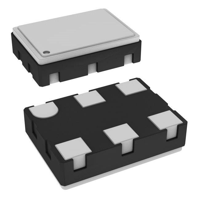
| 描述 | IC OSC VCXO 212MHZ 6CLCC时钟发生器及支持产品 VCXO LVDS 212 MHZ |
| 产品分类 | |
| 品牌 | ON Semiconductor |
| 产品手册 | |
| 产品图片 |
|
| rohs | 符合RoHS无铅 / 符合限制有害物质指令(RoHS)规范要求 |
| 产品系列 | 时钟和计时器IC,时钟发生器及支持产品,ON Semiconductor NBVSPA013LNHTAGPureEdge™ |
| 数据手册 | |
| 产品型号 | NBVSPA013LNHTAG |
| PCN封装 | |
| 产品种类 | 时钟发生器及支持产品 |
| 供应商器件封装 | 6-CLCC(7x5) |
| 其它名称 | NBVSPA013LNHTAGOSDKR |
| 包装 | Digi-Reel® |
| 商标 | ON Semiconductor |
| 安装类型 | 表面贴装 |
| 安装风格 | SMD/SMT |
| 封装 | Reel |
| 封装/外壳 | 6-CLCC |
| 封装/箱体 | CLCC-6 |
| 工作温度 | -40°C ~ 85°C |
| 工作电源电压 | 2.5 V |
| 工作电源电流 | 100 mA |
| 工厂包装数量 | 100 |
| 最大工作温度 | + 85 C |
| 最大输出频率 | 212 MHz |
| 最小工作温度 | - 40 C |
| 标准包装 | 1 |
| 电压-电源 | 2.375 V ~ 2.625 V |
| 电流-电源 | 75mA |
| 类型 | VCXO Clock Generators |
| 系列 | NBVSPA013 |
| 计数 | - |
| 频率 | 212MHz |


PDF Datasheet 数据手册内容提取
NBVSPA013 2.5 V, 212.00 MHz LVDS Voltage-Controlled Clock Oscillator (VCXO) (cid:2) PureEdge Product Series http://onsemi.com The NBVSPA013 voltage−controlled crystal oscillator (VCXO) is designed to meet today’s requirements for 2.5V LVDS clock MARKING DIAGRAMS generation applications. These devices use a high Q fundamental mode crystal and Phase Locked Loop (PLL) multiplier to provide 212.00 MHz with a pullable range of ±100ppm and a frequency NBVSPA013 stability of ±50ppm. The silicon−based PureEdge(cid:2) products design 212.0000 provides users with exceptional frequency stability and reliability. 6 PIN CLCC AWLYYWWG They produce an ultra low jitter and phase noise LVDS differential LN SUFFIX output. CASE 848AB The NBVSPA013 is a member of ON Semiconductor’s PureEdge clock family that provides accurate and precision clock generation A = Assembly Location WL = Wafer Lot solutions. YY = Year Available in the industry standard 5.0 x 7.0 x 1.8 mm SMD (CLCC) WW= Work Week package on 16 mm tape and reel in quantities of 1,000 and 100. G = Pb−Free Package Features • LVDS Differential Output ORDERING INFORMATION • Uses High Q Fundamental Mode Crystal See detailed ordering and shipping information in the • package dimensions section on page 6 of this data sheet. Ultra Low Jitter and Phase Noise − 0.5 ps (12 kHz − 20 MHz) • Pullable Range Minimum of ±100 ppm • Frequency Stability of ±50 ppm • Control Voltage with Positive Slope • Voltage Control Linearity of ±10% • Hermetically Sealed Ceramic SMD Packages of size 5.0 x 7.0 x 1.8mm • Operating Range: 2.5 V ±5% • These Devices are Pb−Free and are RoHS Compliant Applications • Networking • Networking Base Stations • Broadcasting © Semiconductor Components Industries, LLC, 2012 1 Publication Order Number: April, 2012 − Rev. 0 NBVSPA013/D
NBVSPA013 VDD CLK CLK 6 5 4 PLL Crystal Clock Multiplier LVDS 1 2 3 VC OE GND Figure 1. Simplified Logic Diagram VC 1 6 VDD OE 2 5 CLK GND 3 4 CLK Figure 2. Pin Connections (Top View) Table 1. PIN DESCRIPTION Pin No. Symbol I/O Description 1 VC (Note 1) Analog Input Analog control voltage input pin that adjusts output oscillation frequency. f0 =VC = 1.25 V 2 OE LVTTL/LVCMOS Output Enable Pin. When left floating pin defaults to logic HIGH and output is active. Control Input See OE pin description Table 2. 3 GND Power Supply Ground at 0 V. Electrical and Case Ground. 4 CLK LVDS Output Non−Inverted Clock Output. Typically loaded with 100 (cid:2) receiver termination resistor across differential pair. 5 CLK LVDS Output Inverted Clock Output. Typically loaded with 100 (cid:2) receiver termination resistor across differential pair. 6 VDD Power Supply Positive Power Supply Voltage. Voltage should not exceed 2.5 V ±5%. 1. Control voltage has a positive slope with a typical linearity of ±10%; VC = 1.25 V ± 1 V. Table 2. OUTPUT ENABLE TRI−STATE FUNCTION OE Pin Output Pins Open Active HIGH Level Active LOW Level High Z Table 3. ATTRIBUTES Characteristic Value Input Default State Resistor 170 k(cid:2) ESD Protection Human Body Model 2 kV Machine Model 200 V Meets or Exceeds JEDEC Standard EIA/JESD78 IC Latchup Test http://onsemi.com 2
NBVSPA013 Table 4. MAXIMUM RATINGS Symbol Parameter Condition 1 Condition 2 Rating Units VDD Positive Power Supply GND = 0 V 4.6 V VIN Control Input (VC and OE) VIN ≤ VDD + 200 mV V VIN ≥ GND − 200 mV IOSC Output Short Circuit Current CLK to CLK Continuous 12 mA CLK or CLK to GND Continuous 24 TA Operating Temperature Range −40 to +85 °C Tstg Storage Temperature Range −55 to +120 °C Tsol Wave Solder See Figure 5 260 °C Stresses exceeding Maximum Ratings may damage the device. Maximum Ratings are stress ratings only. Functional operation above the Recommended Operating Conditions is not implied. Extended exposure to stresses above the Recommended Operating Conditions may affect device reliability. Table 5. DC CHARACTERISTICS (VDD = 2.5 V ±5%, GND = 0 V, TA = −40°C to +85°C) (Note 2) Symbol Characteristic Conditions Min. Typ. Max. Units IDD Power Supply Current 75 100 mA VIH OE and FSEL Input HIGH Voltage 2000 VDD mV VIL OE and FSEL Input LOW Voltage GND − 300 800 mV IIH Input HIGH Current OE −100 +100 (cid:3)A IIL Input LOW Current OE −100 +100 (cid:3)A (cid:4)VOD Change in Magnitude of VOD for (Note 3) 0 1 25 mV Complementary Output States VOS Offset Voltage 1125 1375 mV (cid:4)VOS Change in Magnitude of VOS for (Note 3) 0 1 25 mV Complementary Output States VOH Output HIGH Voltage 1425 1600 mV VOL Output LOW Voltage 900 1075 mV VOD Differential Output Voltage 250 450 mV NOTE:Device will meet the specifications after thermal equilibrium has been established when mounted in a test socket or printed circuit board with maintained transverse airflow greater than 500 Ifpm. Electrical parameters are guaranteed only over the declared operating temperature range. Functional operation of the device exceeding these conditions is not implied. Device specification limit values are applied individually under normal operating conditions and not valid simultaneously. 2. Measurement taken with outputs terminated with 100 ohm across differential pair. See Figure 4. 3. Parameter guaranteed by design verification not tested in production. http://onsemi.com 3
NBVSPA013 Table 6. AC CHARACTERISTICS (VDD = 2.5 ±5%, GND = 0 V, TA = −40°C to +85°C) (Note 4) Symbol Characteristic Conditions Min. Typ. Max. Unit fCLKOUT Output Clock Frequency NBVSPA013 212.00 MHz (cid:4)f Frequency Stability (Note 5) ±50 ppm tjit((cid:5)) RMS Phase Jitter 12 kHz to 20 MHz 0.4 0.9 ps tjitter Cycle to Cycle, RMS 1000 Cycles 3 8 ps Cycle to Cycle, Peak−to−Peak 1000 Cycles 15 30 ps Period, RMS 10,000 Cycles 2 4 ps Period, Peak−to−Peak 10,000 Cycles 10 20 ps tOE/OD Output Enable/Disable Time 200 ns FP Crystal Pullability (Note 6) 0 V ≤ VC ≤ VDD ±100 ppm VC(bw) Control Voltage Bandwidth −3 dB 20 KHz tDUTY_CYCLE Output Clock Duty Cycle 45 50 55 % (Measured at Cross Point) tR Output Rise Time (20% and 80%) 245 400 ps tF Output Fall Time 245 400 ps (80% and 20%) tstart Start−up Time 1 5 ms Aging 1st Year 3 ppm Every Year After 1st 1 NOTE:Device will meet the specifications after thermal equilibrium has been established when mounted in a test socket or printed circuit board with maintained transverse airflow greater than 500 Ifpm. Electrical parameters are guaranteed only over the declared operating temperature range. Functional operation of the device exceeding these conditions is not implied. Device specification limit values are applied individually under normal operating conditions and not valid simultaneously. 4. Measurement taken with outputs terminated with 100 ohm across differential pair. See Figure 4. 5. Parameter guarantees 10 years of aging. Includes initial stability at 25°C, shock, vibration and first year aging. 6. Gain transfer is positive with a rate of 130 ppm/V. Table 7. PHASE NOISE PERFORMANCE FOR NBVSPA013 Parameter Characteristic Condition 212.00 MHZ Unit (cid:5)NOISE Output Phase−Noise Performance 100 Hz of Carrier −82 dBc/Hz 1 kHz of Carrier −110 dBc/Hz 10 kHz of Carrier −122 dBc/Hz 100 kHz of Carrier −123 dBc/Hz 1 MHz of Carrier −132 dBc/Hz 10 MHz of Carrier −160 dBc/Hz http://onsemi.com 4
NBVSPA013 Figure 3. Typical Phase Noise Plot at 212.00 MHz http://onsemi.com 5
NBVSPA013 Table 8. RELIABILITY COMPLIANCE ÁÁÁÁÁParÁameÁterÁÁÁÁÁÁÁÁSÁtandÁardÁÁÁÁÁÁÁÁÁÁÁMeÁthodÁÁÁÁÁÁ ÁÁÁÁShoÁÁck ÁÁÁÁÁÁÁÁÁÁÁÁÁÁÁÁÁÁMeÁÁchaÁÁnicaÁÁl ÁÁÁÁÁÁÁÁÁÁÁÁÁÁMÁÁIL−ÁÁSTDÁÁ−833ÁÁ, MeÁÁthodÁÁ 200ÁÁ2, CÁÁondÁÁitionÁÁ B ÁÁÁÁÁÁ ÁÁÁÁSoldÁÁeraÁÁbilityÁÁÁÁÁÁÁÁÁÁÁÁÁÁÁÁMeÁÁchaÁÁnicaÁÁl ÁÁÁÁÁÁÁÁÁÁÁÁÁÁMÁÁIL−ÁÁSTDÁÁ−833ÁÁ, MeÁÁthodÁÁ 200ÁÁ3 ÁÁÁÁÁÁÁÁÁÁÁÁ ÁÁÁÁVibrÁÁationÁÁÁÁÁÁÁÁÁÁÁÁÁÁÁÁÁÁMeÁÁchaÁÁnicaÁÁl ÁÁÁÁÁÁÁÁÁÁÁÁÁÁMÁÁIL−ÁÁSTDÁÁ−833ÁÁ, MeÁÁthoÁÁd 20ÁÁ07, CÁÁondÁÁitionÁÁ A ÁÁÁÁÁÁ ÁÁÁÁSolvÁÁent ÁÁResÁÁistanÁÁce ÁÁÁÁÁÁÁÁÁÁÁÁMeÁÁchaÁÁnicaÁÁl ÁÁÁÁÁÁÁÁÁÁÁÁÁÁMÁÁIL−ÁÁSTDÁÁ−202ÁÁ, MeÁÁthodÁÁ 215ÁÁÁÁÁÁÁÁÁÁÁÁÁÁ ÁÁÁÁTheÁÁrmaÁÁl ShoÁÁck ÁÁÁÁÁÁÁÁÁÁÁÁÁÁEnÁÁviroÁÁnmeÁÁnt ÁÁÁÁÁÁÁÁÁÁÁÁÁÁMÁÁIL−ÁÁSTDÁÁ−833ÁÁ, MeÁÁthodÁÁ 10ÁÁ11, CÁÁondÁÁitionÁÁ A ÁÁÁÁÁÁ ÁÁMoiÁstureÁ LevÁel SÁensiÁtivityÁÁÁÁÁEnÁviroÁnmeÁnt ÁÁÁÁÁÁÁMÁSL1Á 260Á°C pÁer IÁPC/JÁEDEÁC J−ÁSTDÁ−02Á0DÁÁÁ NBVSPA013 CLK Zo = 50 (cid:2) D DDreivveicre 100 (cid:2) RDeecveiciever CLK Zo = 50 (cid:2) D Figure 4. Typical Termination for Output Driver and Device Evaluation temp. 260°C Temperature (°C) 20 − 40 sec. max. peak 6°C/sec. max. 260 3°C/sec. max. 217 ramp−up cooling 175 150 pre−heat reflow Time 60(cid:2)180 sec. 60(cid:2)150 sec. Figure 5. Recommended Reflow Soldering Profile Table 9. ORDERING INFORMATION Device Output Frequency (MHz) Package Shipping† 5.0 x 7.0 x 1.8 mm NBVSPA013LN1TAG 212.0000 CLCC−6, Pb−Free 1000 / Tape & Reel NBVSPA013LNHTAG 212.0000 CLCC−6, Pb−Free 100 / Tape & Reel †For information on tape and reel specifications, including part orientation and tape sizes, please refer to our tape and Reel Packaging Specification Brochure, BRD8011/D http://onsemi.com 6
NBVSPA013 PACKAGE DIMENSIONS 6 PIN CLCC, 7x5, 2.54P CASE 848AB ISSUE C D A NOTES: B 1. DIMENSIONING AND TOLERANCING PER D1 ASME Y14.5M, 1994. 4X 0.15 C 2. CONTROLLING DIMENSION: MILLIMETERS. MILLIMETERS DIM MIN NOM MAX A 1.70 1.80 1.90 E2 H E1 E A1 0.70 REF TERMINAL 1 INDICATOR A2 0.36 REF A3 0.08 0.10 0.12 b 1.30 1.40 1.50 D 7.00 BSC D2 D1 6.17 6.20 6.23 D2 6.66 6.81 6.96 TOP VIEW D3 5.08 BSC E 5.00 BSC A3 A2 E1 4.37 4.40 4.43 0.10 C E2 4.65 4.80 4.95 E3 3.49 BSC A e 2.54 BSC H 1.80 REF L 1.17 1.27 1.37 SIDE VIEW R 0.70 REF A1 C SEATING PLANE SOLDERING FOOTPRINT* D3 e 1 2 3 6X R 1.50 E3 5.06 0.10 C A B 6 5 4 0.05 C 6Xb 6XL BOTTOM VIEW 2.54 16.X50 PITCH DIMENSION: MILLIMETERS *For additional information on our Pb−Free strategy and soldering details, please download the ON Semiconductor Soldering and Mounting Techniques Reference Manual, SOLDERRM/D. PureEdge is a trademark of Semiconductor Components Industries, LLC (SCILLC). ON Semiconductor and are registered trademarks of Semiconductor Components Industries, LLC (SCILLC). SCILLC reserves the right to make changes without further notice to any products herein. SCILLC makes no warranty, representation or guarantee regarding the suitability of its products for any particular purpose, nor does SCILLC assume any liability arising out of the application or use of any product or circuit, and specifically disclaims any and all liability, including without limitation special, consequential or incidental damages. “Typical” parameters which may be provided in SCILLC data sheets and/or specifications can and do vary in different applications and actual performance may vary over time. All operating parameters, including “Typicals” must be validated for each customer application by customer’s technical experts. SCILLC does not convey any license under its patent rights nor the rights of others. SCILLC products are not designed, intended, or authorized for use as components in systems intended for surgical implant into the body, or other applications intended to support or sustain life, or for any other application in which the failure of the SCILLC product could create a situation where personal injury or death may occur. Should Buyer purchase or use SCILLC products for any such unintended or unauthorized application, Buyer shall indemnify and hold SCILLC and its officers, employees, subsidiaries, affiliates, and distributors harmless against all claims, costs, damages, and expenses, and reasonable attorney fees arising out of, directly or indirectly, any claim of personal injury or death associated with such unintended or unauthorized use, even if such claim alleges that SCILLC was negligent regarding the design or manufacture of the part. SCILLC is an Equal Opportunity/Affirmative Action Employer. This literature is subject to all applicable copyright laws and is not for resale in any manner. PUBLICATION ORDERING INFORMATION LITERATURE FULFILLMENT: N. American Technical Support: 800−282−9855 Toll Free ON Semiconductor Website: www.onsemi.com Literature Distribution Center for ON Semiconductor USA/Canada P.O. Box 5163, Denver, Colorado 80217 USA Europe, Middle East and Africa Technical Support: Order Literature: http://www.onsemi.com/orderlit Phone: 303−675−2175 or 800−344−3860 Toll Free USA/Canada Phone: 421 33 790 2910 Fax: 303−675−2176 or 800−344−3867 Toll Free USA/Canada Japan Customer Focus Center For additional information, please contact your local Email: orderlit@onsemi.com Phone: 81−3−5817−1050 Sales Representative http://onsemi.com NBVSPA013/D 7