ICGOO在线商城 > 集成电路(IC) > 逻辑 - 缓冲器,驱动器,接收器,收发器 > N74F244D,623

 Datasheet下载
- 型号: N74F244D,623
- 制造商: NXP Semiconductors
- 库位|库存: xxxx|xxxx
- 要求:
| 数量阶梯 | 香港交货 | 国内含税 |
| +xxxx | $xxxx | ¥xxxx |
查看当月历史价格
查看今年历史价格
N74F244D,623产品简介:
ICGOO电子元器件商城为您提供N74F244D,623由NXP Semiconductors设计生产,在icgoo商城现货销售,并且可以通过原厂、代理商等渠道进行代购。 N74F244D,623价格参考¥1.15-¥1.20。NXP SemiconductorsN74F244D,623封装/规格:逻辑 - 缓冲器,驱动器,接收器,收发器, Buffer, Non-Inverting 2 Element 4 Bit per Element 3-State Output 20-SO。您可以下载N74F244D,623参考资料、Datasheet数据手册功能说明书,资料中有N74F244D,623 详细功能的应用电路图电压和使用方法及教程。
NXP USA Inc.生产的N74F244D,623是一款逻辑缓冲器/驱动器/接收器,属于74F系列高速TTL(晶体管-晶体管逻辑)器件。该型号主要用于数据传输和信号处理中的电平转换、信号增强和隔离等应用场景。

 主要功能与特性:
1. 8位双向三态总线收发器:N74F244D可以作为双向三态总线收发器使用,支持8位数据的传输。它可以在两个方向上传输数据,并且可以通过控制信号选择性地使能或禁用输出,从而实现总线共享。

2. 高驱动能力:该器件具有较强的驱动能力,能够驱动多个负载设备,适用于需要大电流驱动的应用场景,如驱动LED、继电器或其他数字电路。

3. 低功耗:相比传统的TTL器件,74F系列具有更低的功耗,适合对功耗敏感的应用场合。

4. 兼容性强:N74F244D与标准的TTL和CMOS逻辑电平兼容,可以方便地与其他逻辑电路集成。

5. 快速开关速度:该器件具有较快的开关速度,适用于高速数据传输场景,确保信号的准确性和完整性。

 应用场景:
1. 计算机系统:在计算机主板、扩展卡等设备中,N74F244D常用于实现数据总线的扩展和隔离,尤其是在多处理器或多总线架构中,它可以有效地管理不同模块之间的数据传输,避免信号冲突。

2. 通信设备:在通信设备中,该器件可用于信号的中继和放大,确保长距离传输时信号的稳定性和完整性。例如,在网络交换机、路由器等设备中,N74F244D可以用于数据包的转发和处理。

3. 工业控制系统:在工业自动化领域,N74F244D可以用于PLC(可编程逻辑控制器)、传感器接口等设备中,负责信号的采集、处理和传输,确保系统的可靠性和实时性。

4. 消费电子:在一些消费电子产品中,如打印机、扫描仪等,N74F244D可以用于内部数据总线的管理和信号的调理,提高设备的性能和稳定性。

总之,N74F244D,623凭借其强大的驱动能力和灵活的信号处理功能,广泛应用于各种需要高效数据传输和信号处理的场景中。
| 参数 | 数值 |
| 产品目录 | 集成电路 (IC)半导体 |
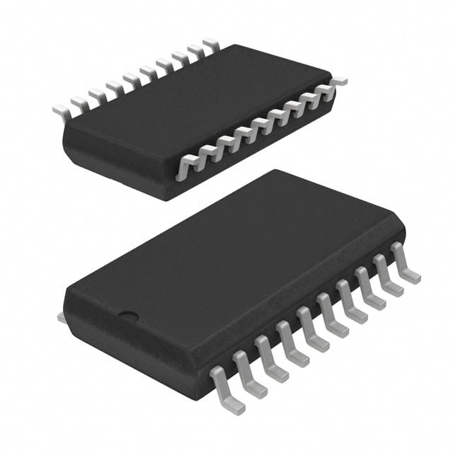
| 描述 | IC BUFF/DVR TRI-ST DUAL 20SOIC缓冲器和线路驱动器 OCTAL BUFFER 3-STATE |
| 产品分类 | |
| 品牌 | NXP Semiconductors |
| 产品手册 | |
| 产品图片 |
|
| rohs | 符合RoHS无铅 / 符合限制有害物质指令(RoHS)规范要求 |
| 产品系列 | 逻辑集成电路,缓冲器和线路驱动器,NXP Semiconductors N74F244D,62374F |
| 数据手册 | |
| 产品型号 | N74F244D,623 |
| PCN封装 | |
| 产品培训模块 | http://www.digikey.cn/PTM/IndividualPTM.page?site=cn&lang=zhs&ptm=24983 |
| 产品目录页面 | |
| 产品种类 | 缓冲器和线路驱动器 |
| 传播延迟时间 | 5.2 ns at 5 V |
| 低电平输出电流 | 64 mA |
| 供应商器件封装 | 20-SO |
| 元件数 | 2 |
| 其它名称 | 568-2323-6 |
| 包装 | Digi-Reel® |
| 商标 | NXP Semiconductors |
| 安装类型 | 表面贴装 |
| 安装风格 | SMD/SMT |
| 封装 | Reel |
| 封装/外壳 | 20-SOIC(0.295",7.50mm 宽) |
| 封装/箱体 | SO-20 |
| 工作温度 | 0°C ~ 70°C |
| 工厂包装数量 | 2000 |
| 最大工作温度 | + 70 C |
| 最小工作温度 | 0 C |
| 极性 | Non-Inverting |
| 标准包装 | 1 |
| 每元件位数 | 4 |
| 每芯片的通道数量 | 8 |
| 电压-电源 | 4.5 V ~ 5.5 V |
| 电流-输出高,低 | 15mA,64mA |
| 电源电压-最大 | 5.5 V |
| 电源电压-最小 | 4.5 V |
| 输入线路数量 | 8 |
| 输出类型 | 3-State |
| 输出线路数量 | 8 |
| 逻辑类型 | 缓冲器/线路驱动器,非反相 |
| 逻辑系列 | F |
| 零件号别名 | N74F244D-T |
| 高电平输出电流 | - 15 mA |


- 商务部:美国ITC正式对集成电路等产品启动337调查
- 曝三星4nm工艺存在良率问题 高通将骁龙8 Gen1或转产台积电
- 太阳诱电将投资9.5亿元在常州建新厂生产MLCC 预计2023年完工
- 英特尔发布欧洲新工厂建设计划 深化IDM 2.0 战略
- 台积电先进制程称霸业界 有大客户加持明年业绩稳了
- 达到5530亿美元!SIA预计今年全球半导体销售额将创下新高
- 英特尔拟将自动驾驶子公司Mobileye上市 估值或超500亿美元
- 三星加码芯片和SET,合并消费电子和移动部门,撤换高东真等 CEO
- 三星电子宣布重大人事变动 还合并消费电子和移动部门
- 海关总署:前11个月进口集成电路产品价值2.52万亿元 增长14.8%


PDF Datasheet 数据手册内容提取
INTEGRATED CIRCUITS 74F244/74F244B Octal buffers (3-State) Product specification 1994 Dec 05 IC15 Data Handbook Philips Semiconductors
Philips Semiconductors Product specification Octal buffers (3-State) 74F244/74F244B FEATURES DESCRIPTION •Octal bus interface The 74F244 is an octal buffer that is ideal for driving bus lines of buffer memory address registers. The outputs are all capable of • 3-State output buffer sink 64mA sinking 64mA and sourcing up to 15mA, producing very good • capacitive drive characteristics. The device features two output 15mA source current enables, OEa and OEb, each controlling four of the 3-State outputs. • Guaranteed output skew less than 2.0ns (74F244B) The 74F244B is functionally equivalent to the 74F244. It has been • Reduced ground bounce (74F244B) designed to reduce effects of ground noise. Other advantages are • noted in the features. Reduced ICC (74F244B) • Reduced loading (74F244B IIL = 40m A) TYPICAL TYPICAL SUPPLY • TYPE PROPAGATION Split lead frame offers increased noise immunity (74F244B) CURRENT (TOTAL) DELAY • Industrial temperature range available (-40°C to +85°C) for 74F244 4.0ns 53mA 74F244 74F244B 4.0ns 33mA • 74F244 available in SSOP Type II package ORDERING INFORMATION ORDER CODE COMMERCIAL RANGE INDUSTRIAL RANGE PPKKGG DDWWGG ## DESCRIPTION VCC = 5V ±10%, VCC = 5V ±10%, ° ° ° ° Tamb = 0 C to +70 C Tamb = -40 C to +85 C 20-pin plastic DIP N74F244N, N74F244BN I74F244N SOT146-1 20-pin plastic SOL N74F244D, N74F244BD I74F244D SOT163-1 20-pin plastic SSOP II N74F244DB SOT339-1 INPUT AND OUTPUT LOADING AND FAN OUT TABLE 74F (U.L.) LOAD VALUE PINS DESCRIPTION HIGH/LOW HIGH/LOW Ian, Ibn Data inputs (74F244) 1.0/2.67 20m A/1.6mA Data inputs (74F244B) 1.0/0.067 20m A/40m A OEa, OEb Output enable inputs (active low) (74F244) 1.0/1.67 20m A/1.0mA Output enable inputs (active low) (74F244B) 1.0/0.067 20m A/40m A Yan, Ybn Data outputs 750/106.7 15mA/64mA NOTE: One (1.0) FAST unit load is defined as: 20m A in the high state and 0.6mA in the low state. PIN CONFIGURATION LOGIC SYMBOL OEa 1 20 VCC 2 4 6 8 17 15 13 11 Ia0 2 19 OEb Yb0 3 18 Ya0 Ia0 Ia1 Ia2 Ia3 Ib0 Ib1 Ib2 Ib3 Ia1 4 17 Ib0 Yb1 5 16 Ya1 1 OEa Ia2 6 15 Ib1 19 OEb Yb2 7 14 Ya2 Ya0 Ya1 Ya2 Ya3 Yb0 Yb1 Yb2 Yb3 Ia3 8 13 Ib2 Yb3 9 12 Ya3 18 16 14 12 3 5 7 9 GND 10 11 Ib3 VCC = Pin 20 GND = Pin 10 SF00227 SF00228 1994 Dec 5 2 853-0357 14381
Philips Semiconductors Product specification Octal buffers (3-State) 74F244/74F244B IEC/IEEE SYMBOL FUNCTION TABLE INPUTS OUTPUTS 1 EN1 OEa Ia OEb Ib Ya Yb 19 EN2 L L L L L L 2 2D 1 18 L H L H H H 4 16 H X H X Z Z 6 14 NOTES: 8 12 H = High voltage level 17 2 3 L = Low voltage level 15 5 X = Don’t care Z = High impedance ”off” state 13 7 11 9 SF00229 LOGIC DIAGRAM Ia0 2 18 Ya0 Ib0 17 3 Yb0 Ia1 4 16 Ya1 Ib1 15 5 Yb1 Ia2 6 14 Ya2 Ib2 13 7 Yb2 Ia3 8 12 Ya3 Ib3 11 9 Yb3 OEa 1 OEb 19 VCC = Pin 20 GND = Pin 10 SF00230 1994 Dec 5 3
Philips Semiconductors Product specification Octal buffers (3-State) 74F244/74F244B ABSOLUTE MAXIMUM RATINGS (Operation beyond the limit set forth in this table may impair the useful life of the device. Unless otherwise noted these limits are over the operating free air temperature range.) SYMBOL PARAMETER RATING UNIT VCC Supply voltage -0.5 to +7.0 V VIN Input voltage -0.5 to +7.0 V IIN Input current -30 to +5 mA VOUT Voltage applied to output in high output state -0.5 to VCC V IOUT Current applied to output in low output state 128 mA ° Commercial range 0 to +70 C TTamb OOperattiing ffree aiir ttemperatture range Industrial range ° -40 to +85 C (74F244 only) Tstg Storage temperature range -65 to +150 °C RECOMMENDED OPERATING CONDITIONS LIMITS SSYYMMBBOOLL PPAARRAAMMEETTEERR UUNNIITT MIN NOM MAX VCC Supply voltage 4.5 5.0 5.5 V VIN High-level input voltage 2.0 V VIL Low-level input voltage 0.8 V IIK Input clamp current –18 mA IOH High-level output current –15 mA iol Low-level output current 64 mA ° Commercial range 0 +70 C TTamb OOperattiing ffree aiir ttemperatture range Industrial range ° –40 +85 C (74F244 only) 1994 Dec 5 4
Philips Semiconductors Product specification Octal buffers (3-State) 74F244/74F244B DC ELECTRICAL CHARACTERISTICS (Over recommended operating free-air temperature range unless otherwise noted.) TEST LIMITS SSYYMMBBOOLL PPAARRAAMMEETTEERR CONDITIONS1 MIN TYP2 MAX UUNNIITT VCC = MIN, IOH = -3mA ±10%VCC 2.5 V VOH High-level output voltage VIL = MAX, ±5%VCC 2.7 3.4 V VIH = MIN IOH = -15mA ±10%VCC 2.0 V ±5%VCC 2.0 V VOL Low-level output voltage VVCILC = = M MAIXN,, IOL = MAX ±10%VCC 0.55 V VIH = MIN, ±5%VCC 0.42 0.55 V VIK Input clamp voltage VCC = MIN, II = IIK -0.73 -1.2 V II Input current at maximum input voltage VCC = MAX, VI = 7.0V 100 m A IIH High-level input current VCC = MAX, VI = 2.7V 20 m A 74F244 OEa, OEb -1.0 mA IIL Low-level input current 74F244 Ian, Ibn VCC = MAX, VI = 0.5V -1.6 mA 74F244B all inputs -40 m A IOZH Ohifgf-hs-tlaetvee lo vuotpltuatg ceu arrpepnlite,d VCC = MAX, VO = 2.7V 50 m A IOZL Olofwf--sletavteel ovuotltpaugte c auprrpelniet,d VCC = MAX, VO = 0.5V -50 m A IOS Short-circuit output current3 VCC = MAX -100 -225 mA ICCH 40 60 mA 74F244 ICCL VCC = MAX 60 90 mA ICC Supply current (total) ICCZ 60 90 mA ICCH 20 30 mA 74F244B ICCL VCC = MAX 50 70 mA ICCZ 29 40 mA NOTES: 1. For conditions shown as MIN or MAX, use the appropriate value specified under recommended operating conditions for the applicable type. ° 2. All typical values are at VCC = 5V, Tamb = 25 C. 3. Not more than one output should be shorted at a time. For testing IOS, the use of high-speed test apparatus and/or sample-and-hold techniques are preferable in order to minimize internal heating and more accurately reflect operational values. Otherwise, prolonged shorting of a high output may raise the chip temperature well above normal and thereby cause invalid readings in other parameter tests. In any sequence of parameter tests, IOS tests should be performed last. 1994 Dec 5 5
Philips Semiconductors Product specification Octal buffers (3-State) 74F244/74F244B AC ELECTRICAL CHARACTERISTICS FOR 74F244 A PORT LIMITS ° ° ° ° ° Tamb = +25 C Tamb = 0 C to +70 C Tamb = -40 C to +85 C ± ± SYMBOL PARAMETER TEST VCC = +5.0V VCC = +5.0V 10% VCC = +5.0V 10% UNIT CONDITION CL = 50pF, CL = 50pF, CL = 50pF, RL = 500W RL = 500W RL = 500W MIN TYP MAX MIN MAX MIN MAX tPLH Propagation delay Waveform 1 2.5 4.0 5.2 2.0 6.2 1.5 7.0 ns tPHL Ian, Ibn to Yn 2.5 4.0 5.2 2.0 6.5 2.0 7.0 tPZH Output enable time Waveform 2 2.0 4.3 5.7 2.0 6.7 2.0 8.0 ns tPZL to high or low Waveform 4 2.0 5.0 7.0 2.0 8.0 2.0 8.5 tPHZ Output disable time Waveform 2 1.5 2.5 5.5 1.0 6.0 1.0 6.0 ns tPLZ from high or low Waveform 4 1.5 2.5 5.5 1.0 5.5 1.0 5.5 AC ELECTRICAL CHARACTERISTICS FOR 74F244B LIMITS ° ° ° Tamb = +25 C Tamb = 0 C to +70 C ± SYMBOL PARAMETER TEST VCC = +5.0V VCC = +5.0V 10% UNIT CONDITION CL = 50pF, RL = 500W CL = 50pF, RL = 500W MIN TYP MAX MIN MAX tPLH Propagation delay Waveform 1 2.5 4.5 5.7 2.0 6.2 ns tPHL Ian, Ibn to Yn 2.5 4.5 6.0 2.5 6.5 tPZH Output enable time Waveform 2 2.0 4.0 6.0 2.0 6.5 ns tPZL to high or low level Waveform 4 3.0 5.5 7.5 3.0 8.0 tPHZ Output disable time Waveform 2 1.5 2.5 5.5 1.0 6.0 ns tPLZ from high or low level Waveform 4 1.5 2.5 5.5 1.0 5.5 tsk(0) Output skew1, 2 Waveform 3 1.5 2.0 ns NOTES: 1. |tPN actual - tPM actual| for any output compared to any other output where N and M are either LH or HL. 2. Skew times are valid only under same test conditions (temperature, VCC, loading, etc.,). 1994 Dec 5 6
Philips Semiconductors Product specification Octal buffers (3-State) 74F244/74F244B AC WAVEFORMS For all waveforms, VM = 1.5V. Ian, Ibn VM VM Yn, Yn VM tPLH tPHL tsk(0) Yn VM VM Yn, Yn VM SF00231 SF00232 Waveform 1. Propagation Delay for data to outputs Waveform 3. Output skew OEn VM VM OEn VM VM tPZH tPHZ tPZL tPLZ 3.5V VOH–0.3V Yn VM Yn VM 0V VOL+0.3V SF00233 SF00234 Waveform 2. 3-State output enable time to high level Waveform 4. 3-State output enable time to low level and output disable time from high level and output disable time from low level TEST CIRCUIT AND WAVEFORMS SWITCH POSITION TEST SWITCH tw AMP (V) 90% 90% tPLZ, tPZL closed VCC 7.0V NPUEGLSAETIVE VM VM All other open 10% 10% 0V VIN VOUT RL tTHL (tf ) tTLH (tr ) PULSE D.U.T. GENERATOR tTLH (tr ) tTHL (tf ) RT CL RL AMP (V) 90% 90% POSITIVE PULSE VM VM Test circuit for 3-State outputs 10% 10% DEFINITIONS: tw 0V RL = Load resistor; see AC electrical characteristics for Input pulse definition value. CL = Load capacitance includes jig and probe family INPUT PULSE REQUIREMENTS capacitance; see AC electrical characteristics for value amplitude VM rep. rate tw tTLH tTHL RT = Termination resistance should be equal to ZOUT of 74F 3.0V 1.5V 1MHz 500ns 2.5ns 2.5ns pulse generators. SF000235 1994 Dec 5 7
Philips Semiconductors Product specification Octal buffers (3-State) 74F244/74F244B DIP20: plastic dual in-line package; 20 leads (300 mil) SOT146-1 1994 Dec 05 8
Philips Semiconductors Product specification Octal buffers (3-State) 74F244/74F244B SO20: plastic small outline package; 20 leads; body width 7.5 mm SOT163-1 1994 Dec 05 9
Philips Semiconductors Product specification Octal buffers (3-State) 74F244/74F244B SSOP20: plastic shrink small outline package; 20 leads; body width 5.3 mm SOT339-1 1994 Dec 05 10
Philips Semiconductors Product specification Octal buffers (3-State) 74F244/74F244B NOTES 1994 Dec 05 11
Philips Semiconductors Product specification Octal buffers (3-State) 74F244/74F244B DEFINITIONS Data Sheet Identification Product Status Definition This data sheet contains the design target or goal specifications for product development. Specifications Objective Specification Formative or in Design 9397-750-05103 may change in any manner without notice. This data sheet contains preliminary data, and supplementary data will be published at a later date. Philips Preliminary Specification Preproduction Product Semiconductors reserves the right to make changes at any time without notice in order to improve design and supply the best possible product. This data sheet contains Final Specifications. Philips Semiconductors reserves the right to make changes Product Specification Full Production at any time without notice, in order to improve design and supply the best possible product. Philips Semiconductors and Philips Electronics North America Corporation reserve the right to make changes, without notice, in the products, including circuits, standard cells, and/or software, described or contained herein in order to improve design and/or performance. Philips Semiconductors assumes no responsibility or liability for the use of any of these products, conveys no license or title under any patent, copyright, or mask work right to these products, and makes no representations or warranties that these products are free from patent, copyright, or mask work right infringement, unless otherwise specified. Applications that are described herein for any of these products are for illustrative purposes only. Philips Semiconductors makes no representation or warranty that such applications will be suitable for the specified use without further testing or modification. LIFE SUPPORT APPLICATIONS Philips Semiconductors and Philips Electronics North America Corporation Products are not designed for use in life support appliances, devices, or systems where malfunction of a Philips Semiconductors and Philips Electronics North America Corporation Product can reasonably be expected to result in a personal injury. Philips Semiconductors and Philips Electronics North America Corporation customers using or selling Philips Semiconductors and Philips Electronics North America Corporation Products for use in such applications do so at their own risk and agree to fully indemnify Philips Semiconductors and Philips Electronics North America Corporation for any damages resulting from such improper use or sale. Philips Semiconductors Philips Semiconductors and Philips Electronics North America Corporation 811 East Arques Avenue register eligible circuits under the Semiconductor Chip Protection Act. P.O. Box 3409 Copyright Philips Electronics North America Corporation 1996 Sunnyvale, California 94088–3409 All rights reserved. Printed in U.S.A. Telephone 800-234-7381 (print code) Date of release: October 28, 1991 Document order number: 9397-750-05103