ICGOO在线商城 > 分立半导体产品 > 二极管 - 整流器 - 阵列 > MUR1620CTG
 Datasheet下载
- 型号: MUR1620CTG
- 制造商: ON Semiconductor
- 库位|库存: xxxx|xxxx
- 要求:
| 数量阶梯 | 香港交货 | 国内含税 |
| +xxxx | $xxxx | ¥xxxx |
查看当月历史价格
查看今年历史价格
MUR1620CTG产品简介:
ICGOO电子元器件商城为您提供MUR1620CTG由ON Semiconductor设计生产,在icgoo商城现货销售,并且可以通过原厂、代理商等渠道进行代购。 MUR1620CTG价格参考¥4.66-¥5.92。ON SemiconductorMUR1620CTG封装/规格:二极管 - 整流器 - 阵列, Diode Array 1 Pair Common Cathode Standard 200V 8A Through Hole TO-220-3。您可以下载MUR1620CTG参考资料、Datasheet数据手册功能说明书,资料中有MUR1620CTG 详细功能的应用电路图电压和使用方法及教程。
MUR1620CTG 是 ON Semiconductor 生产的一款二极管整流器阵列,属于超快速恢复二极管(Ultrafast Recovery Diode)。它具有低正向电压降和非常短的反向恢复时间,适用于需要高效能和高可靠性的电源管理电路中。以下是该型号的一些典型应用场景:

 1. 开关电源(SMPS)
MUR1620CTG 的低正向压降和快速恢复特性使其非常适合用于开关电源中的整流部分。它可以有效减少开关损耗,提高电源转换效率,特别适合于高频开关电源设计。在这些应用中,二极管需要快速响应电流的变化,以确保系统的稳定性和效率。

 2. 逆变器和电机驱动
在逆变器和电机驱动应用中,MUR1620CTG 可以用作续流二极管(Flyback Diode),帮助吸收感性负载(如电机绕组)产生的反电动势,防止电压尖峰对其他元件造成损坏。其快速恢复特性可以减少能量损失,提升系统的整体性能。

 3. 光伏系统
在太阳能光伏发电系统中,MUR1620CTG 可以用于最大功率点跟踪(MPPT)控制器或逆变器模块中。由于其高效的整流性能,能够最大限度地减少能量损耗,确保光伏系统的输出功率最大化。

 4. 不间断电源(UPS)
在不间断电源系统中,MUR1620CTG 可以用于电池充电电路和逆变电路中,确保在市电中断时能够迅速切换到备用电源,并且在整个过程中保持稳定的电力输出。其快速恢复特性有助于减少切换时的瞬态冲击。

 5. 通信设备
在通信设备中,MUR1620CTG 可以用于电源模块中的整流和保护电路,确保设备在各种工作条件下都能稳定运行。其低损耗特性有助于提高通信设备的能效,延长使用寿命。

总之,MUR1620CTG 凭借其优异的电气性能和可靠性,广泛应用于各类电源管理和电力电子设备中,尤其适合对效率和响应速度有较高要求的应用场景。
| 参数 | 数值 |
| 产品目录 | |
| 描述 | DIODE ARRAY 200V 8A TO220AB整流器 200V 16A UltraFast |
| 产品分类 | 二极管,整流器 - 阵列分离式半导体 |
| 品牌 | ON Semiconductor |
| 产品手册 | |
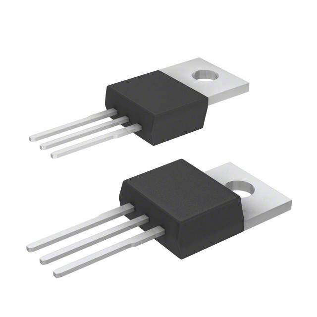
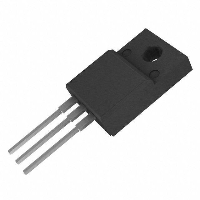
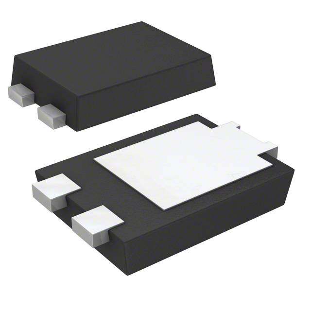
| 产品图片 |
|
| rohs | 符合RoHS无铅 / 符合限制有害物质指令(RoHS)规范要求 |
| 产品系列 | 二极管与整流器,整流器,ON Semiconductor MUR1620CTGSWITCHMODE™ |
| 数据手册 | |
| 产品型号 | MUR1620CTG |
| PCN设计/规格 | |
| 不同If时的电压-正向(Vf) | 975mV @ 8A |
| 不同 Vr时的电流-反向漏电流 | 5µA @ 200V |
| 二极管类型 | 标准 |
| 二极管配置 | 1 对共阴极 |
| 产品 | Ultra Fast Recovery Rectifiers |
| 产品目录页面 | |
| 产品种类 | 整流器 |
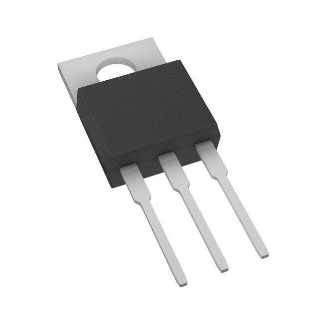
| 供应商器件封装 | TO-220AB |
| 其它名称 | MUR1620CTGOS |
| 包装 | 管件 |
| 反向恢复时间(trr) | 35ns |
| 反向电压 | 200 V |
| 反向电流IR | 5 uA |
| 商标 | ON Semiconductor |
| 安装类型 | 通孔 |
| 安装风格 | Through Hole |
| 封装 | Tube |
| 封装/外壳 | TO-220-3 |
| 封装/箱体 | TO-220-3 |
| 工厂包装数量 | 50 |
| 恢复时间 | 35 ns |
| 最大工作温度 | + 175 C |
| 最大浪涌电流 | 100 A |
| 最小工作温度 | - 65 C |
| 标准包装 | 50 |
| 正向电压下降 | 0.975 V |
| 正向连续电流 | 16 A |
| 热阻 | 3°C/W Jc |
| 电压-DC反向(Vr)(最大值) | 200V |
| 电流-平均整流(Io)(每二极管) | 8A |
| 系列 | MUR1620CT |
| 速度 | 快速恢复 =< 500 ns,> 200mA(Io) |
| 配置 | Dual Common Cathode |


- 商务部:美国ITC正式对集成电路等产品启动337调查
- 曝三星4nm工艺存在良率问题 高通将骁龙8 Gen1或转产台积电
- 太阳诱电将投资9.5亿元在常州建新厂生产MLCC 预计2023年完工
- 英特尔发布欧洲新工厂建设计划 深化IDM 2.0 战略
- 台积电先进制程称霸业界 有大客户加持明年业绩稳了
- 达到5530亿美元!SIA预计今年全球半导体销售额将创下新高
- 英特尔拟将自动驾驶子公司Mobileye上市 估值或超500亿美元
- 三星加码芯片和SET,合并消费电子和移动部门,撤换高东真等 CEO
- 三星电子宣布重大人事变动 还合并消费电子和移动部门
- 海关总署:前11个月进口集成电路产品价值2.52万亿元 增长14.8%


PDF Datasheet 数据手册内容提取
MUR1610CTG, MUR1615CTG, MUR1620CTG, MUR1640CTG, MUR1660CTG Switch Mode Power Rectifiers www.onsemi.com These state−of−the−art devices are a series designed for use in switching power supplies, inverters and as free wheeling diodes. ULTRAFAST RECTIFIERS Features 16 AMPERES, 100−600 VOLTS • Ultrafast 35 and 60 Nanosecond Recovery Times • 175°C Operating Junction Temperature • Popular TO−220 Package 1 • Epoxy Meets UL 94 V−0 @ 0.125 in 2, 4 • High Temperature Glass Passivated Junction 3 • High Voltage Capability to 600 V • Low Leakage Specified @ 150°C Case Temperature • Current Derating @ Both Case and Ambient Temperatures 4 • These are Pb−Free Devices* Mechanical Characteristics: • Case: Epoxy, Molded • Weight: 1.9 Grams (Approximately) TO−220AB • CASE 221A−09 Finish: All External Surfaces Corrosion Resistant and Terminal Leads are Readily Solderable 1 • 2 Lead Temperature for Soldering Purposes: 3 260°C Max. for 10 Seconds MARKING DIAGRAM AY WW U16xxG AKA A =Assembly Location Y =Year WW =Work Week U16xx =Device Code xx = 10, 15, 20, 40 or 60 G =Pb−Free Package KA =Diode Polarity *For additional information on our Pb−Free strategy and soldering details, please download the ON Semiconductor Soldering and Mounting Techniques ORDERING INFORMATION Reference Manual, SOLDERRM/D. See detailed ordering and shipping information in the package dimensions section on page 6 of this data sheet. © Semiconductor Components Industries, LLC, 2015 1 Publication Order Number: January, 2015 − Rev. 8 MUR1620CT/D
MUR1610CTG, MUR1615CTG, MUR1620CTG, MUR1640CTG, MUR1660CTG MAXIMUM RATINGS MUR16 Rating Symbol 10CT 15CT 20CT 40CT 60CT Unit Peak Repetitive Reverse Voltage VRRM 100 150 200 400 600 V Working Peak Reverse Voltage VRWM DC Blocking Voltage VR Average Rectified Forward Current Per Leg IF(AV) 8.0 A Total Device, (Rated VR), TC = 150°C Total Device 16 Peak Rectified Forward Current Per Diode Leg IFM 16 A (Rated VR, Square Wave, 20 kHz), TC = 150°C Nonrepetitive Peak Surge Current IFSM 100 A (Surge applied at rated load conditions halfwave, single phase, 60 Hz) Operating Junction Temperature and Storage Temperature TJ, Tstg (cid:2)65 to +175 °C Stresses exceeding those listed in the Maximum Ratings table may damage the device. If any of these limits are exceeded, device functionality should not be assumed, damage may occur and reliability may be affected. THERMAL CHARACTERISTICS (Per Diode Leg) Parameter Symbol Value Unit Maximum Thermal Resistance, Junction−to−Case R(cid:2)JC 3.0 2.0 °C/W ELECTRICAL CHARACTERISTICS (Per Diode Leg) Characteristic Symbol 1620 1640 1660 Unit Maximum Instantaneous Forward Voltage (Note 1) vF V (iF = 8.0 A, TC = 150°C) 0.895 1.00 1.20 (iF = 8.0 A, TC = 25°C) 0.975 1.30 1.50 Maximum Instantaneous Reverse Current (Note 1) iR (cid:3)A (Rated DC Voltage, TC = 150°C) 250 500 (Rated DC Voltage, TC = 25°C) 5.0 10 Maximum Reverse Recovery Time trr ns (IF = 1.0 A, di/dt = 50 A/(cid:3)s) 35 60 (IF = 0.5 A, IR = 1.0 A, IREC = 0.25 A) 25 50 Product parametric performance is indicated in the Electrical Characteristics for the listed test conditions, unless otherwise noted. Product performance may not be indicated by the Electrical Characteristics if operated under different conditions. 1. Pulse Test: Pulse Width = 300 (cid:3)s, Duty Cycle ≤2.0% www.onsemi.com 2
MUR1610CTG, MUR1615CTG, MUR1620CTG, MUR1640CTG, MUR1660CTG MUR1610CT, MUR1615CT, MUR1620CT 100 800 400 70 200 A) 50 (cid:3)NT ( 4800 TJ = 175°C E 20 R UR 8.0 30 E C 4.0 100°C S 2.0 R 20 REVE 00..84 25°C S) TJ = 175°C 100°C I, R 0.2 P 0.08 M 10 A 0.04 T ( 0.02 N E 7.0 RR 25°C 0 20 40 60 80 100 120 140 160 180 200 U D C 5.0 VR, REVERSE VOLTAGE (VOLTS) R A Figure 2. Typical Reverse Current, Per Leg* W R O 3.0 * The curves shown are typical for the highest voltage device in the F S voltage grouping. Typical reverse current for lower voltage selections U EO 2.0 can be estimated from these same curves if VR is sufficiently below AN rated VR. T N , INSTAiF 10..07 N (WATTS) 981..000 RATED VR APPLIED O ATI 7.0 0.5 P SI S 6.0 DI R 5.0 0.3 E W O 4.0 dc P 0.2 E G 3.0 A R E 2.0 SQUARE WAVE V A 0.1 , V) 1.0 0.2 0.3 0.4 0.5 0.6 0.7 0.8 0.9 1.0 1.1 1.2 F(A 0 vF, INSTANTANEOUS VOLTAGE (VOLTS) I 140 145 150 155 160 165 170 175 180 Figure 1. Typical Forward Voltage, Per Leg TC, CASE TEMPERATURE (°C) Figure 3. Current Derating, Case, Per Leg RD CURRENT (AMPS) 8111.0240 dc R(RN(cid:2)(cid:2)OJJAA H ==E 16A60T°°SCCIN//WWK) DISSIPATION (WATTS) 67891....00000 TJ = 175°C SQUARE WAVE dc WA SQUARE WAVE ER 5.0 R 6.0 W O O 4.0 F P AGE 4.0 dc AGE 3.0 R R E E 2.0 I, AVF(AV) 2.00 0 SQ2U0ARE 4W0AVE60 80 100 120 140 160 180 200 P, AVF(AV) 1.00 0 1.0 2.0 3.0 4.0 5.0 6.0 7.0 8.0 9.0 10 TA, AMBIENT TEMPERATURE (°C) IF(AV), AVERAGE FORWARD CURRENT (AMPS) Figure 4. Current Derating, Ambient, Per Leg Figure 5. Power Dissipation, Per Leg www.onsemi.com 3
MUR1610CTG, MUR1615CTG, MUR1620CTG, MUR1640CTG, MUR1660CTG MUR1640CT 100 800 400 70 200 50 (cid:3)NT ( A) 4800 TJ 1=5 107°5C°C E 20 R UR 8.0 30 E C 4.0 100°C PS) 20 TJ = 175°C 100°C25°C REVERS 002...840 AM , R 0.2 25°C T ( I 0.08 N 10 E 0.04 R R 0.02 U C 7.0 D 0 50 100 150 200 250 300 350 400 450 500 R A W 5.0 VR, REVERSE VOLTAGE (VOLTS) R O Figure 7. Typical Reverse Current, Per Leg* F S OU 3.0 * The curves shown are typical for the highest voltage device in the E N voltage grouping. Typical reverse current for lower voltage selections NTA 2.0 can be estimated from these curves if VR is sufficiently below rated TA VR. S N , IF 1.0 TS) 10 i WAT 9.0 RATED VR APPLIED 0.7 N ( 8.0 O ATI 7.0 0.5 P SI S 6.0 DI R 5.0 0.3 E W O 4.0 dc P 0.2 E G 3.0 A R E 2.0 SQUARE WAVE V A 0.1 , V) 1.0 0.4 0.6 0.8 1.0 1.2 1.4 1.6 F(A 0 vF, INSTANTANEOUS VOLTAGE (VOLTS) I 140 145 150 155 160 165 170 175 180 Figure 6. Typical Forward Voltage, Per Leg TC, CASE TEMPERATURE (°C) Figure 8. Current Derating, Case, Per Leg RD CURRENT (AMPS) 8111.0240 dc RR(N(cid:2)(cid:2)OJJAA H ==E 16A60T°°SCCIN//WWK) DISSIPATION (WATTS) 67891....00000 TJ = 175°C SQUARE WAVE dc WA ER 5.0 R 6.0 SQUARE WAVE W O O 4.0 F P AGE 4.0 dc AGE 3.0 R R E E 2.0 I, AVF(AV) 2.00 0 SQ2U0ARE 4W0AVE60 80 100 120 140 160 180 200 P, AVF(AV) 1.00 0 1.0 2.0 3.0 4.0 5.0 6.0 7.0 8.0 9.0 10 TA, AMBIENT TEMPERATURE (°C) IF(AV), AVERAGE FORWARD CURRENT (AMPS) Figure 9. Current Derating, Ambient, Per Leg Figure 10. Power Dissipation, Per Leg www.onsemi.com 4
MUR1610CTG, MUR1615CTG, MUR1620CTG, MUR1640CTG, MUR1660CTG MUR1660CT 100 800 400 70 A) 200 TJ = 150°C 50 (cid:3)T ( 4800 EN 20 100°C R UR 8.0 30 TJ = 150°C SE C 42..00 R PS) 20 REVE 00..84 25°C T (AM 100°C I, R 00.0.28 EN 10 25°C 0.04 R R 0.02 U C 7.0 D 100 200 300 400 500 600 R A W 5.0 VR, REVERSE VOLTAGE (VOLTS) R O Figure 12. Typical Reverse Current, Per Leg* F S OU 3.0 * The curves shown are typical for the highest voltage device in the E N voltage grouping. Typical reverse current for lower voltage selections NTA 2.0 can be estimated from these same curves if VR is sufficiently below TA rated VR. S N , IF 1.0 TS) 10 i WAT 9.0 RATED VR APPLIED 0.7 N ( 8.0 O ATI 7.0 0.5 P SI S 6.0 DI R 5.0 0.3 E W O 4.0 dc P 0.2 E G 3.0 A R E 2.0 SQUARE WAVE V A 0.1 , V) 1.0 0.4 0.6 0.8 1.0 1.2 1.4 1.6 1.8 F(A 0 vF, INSTANTANEOUS VOLTAGE (VOLTS) I 140 145 150 155 160 165 170 175 180 Figure 11. Typical Forward Voltage, Per Leg TC, CASE TEMPERATURE (°C) Figure 13. Current Derating, Case, Per Leg RD CURRENT (AMPS) 67891....00000 SQUARE WAVdEc R(RN(cid:2)(cid:2)OJJAA H ==E 16A60T°°SCCIN//WWK) DISSIPATION (WATTS) 8911111..0234001 TJ = 175°C SQUARE WAVE dc WA 5.0 ER 7.0 R W 6.0 O 4.0 O AGE F 3.0 dc AGE P 45..00 ER 2.0 ER 3.0 I, AVF(AV) 1.00 0 SQ2U0ARE W40AVE60 80 100 120 140 160 180 200 P, AVF(AV) 12..000 0 1.0 2.0 3.0 4.0 5.0 6.0 7.0 8.0 9.0 10 TA, AMBIENT TEMPERATURE (°C) IF(AV), AVERAGE FORWARD CURRENT (AMPS) Figure 14. Current Derating, Ambient, Per Leg Figure 15. Power Dissipation, Per Leg www.onsemi.com 5
MUR1610CTG, MUR1615CTG, MUR1620CTG, MUR1640CTG, MUR1660CTG D) ZE 1.0 LI MA D = 0.5 R 0.5 O N E ( C AN 0.2 T S 0.1 SI E 0.1 L R 0.05 Z(cid:2)JC(t) = r(t) R(cid:2)JC RMA 0.05 P(pk) D CURVES APPLY FOR POWER HE 0.01 t1 PULSE TRAIN SHOWN T T t2 READ TIME AT T1 N SIE 0.02 SINGLE PULSE DUTY CYCLE, D = t1/t2 TJ(pk) - TC = P(pk) Z(cid:2)JC(t) N RA 0.01 r(t), T 0.01 0.02 0.05 0.1 0.2 0.5 1.0 t, 2T.I0ME (ms) 5.0 10 20 50 100 200 500 1000 Figure 16. Thermal Response 1000 MUR1620CT THRU 1660CT MUR1605CT THRU 1615CT E (pF) 300 TJ = 25°C C N A CIT 100 A P A C C, 30 10 1.0 10 100 VR, REVERSE VOLTAGE (VOLTS) Figure 17. Typical Capacitance, Per Leg ORDERING INFORMATION Device Package Shipping† MUR1610CTG TO−220 (Pb−Free) MUR1615CTG TO−220 (Pb−Free) MUR1620CTG TO−220 50 Units / Rail (Pb−Free) MUR1640CTG TO−220 (Pb−Free) MUR1660CTG TO−220 (Pb−Free) †For information on tape and reel specifications, including part orientation and tape sizes, please refer to our Tape and Reel Packaging Specifications Brochure, BRD8011/D. www.onsemi.com 6
MUR1610CTG, MUR1615CTG, MUR1620CTG, MUR1640CTG, MUR1660CTG PACKAGE DIMENSIONS TO−220 CASE 221A−09 ISSUE AH NOTES: 1. DIMENSIONING AND TOLERANCING PER ANSI Y14.5M, 1982. −T− SPELAATNIENG 2. CONTROLLING DIMENSION: INCH. 3. DIMENSION Z DEFINES A ZONE WHERE ALL B F C BODY AND LEAD IRREGULARITIES ARE T S ALLOWED. INCHES MILLIMETERS 4 DIM MIN MAX MIN MAX A 0.570 0.620 14.48 15.75 Q A B 0.380 0.415 9.66 10.53 C 0.160 0.190 4.07 4.83 1 2 3 U D 0.025 0.038 0.64 0.96 F 0.142 0.161 3.61 4.09 H G 0.095 0.105 2.42 2.66 H 0.110 0.161 2.80 4.10 K J 0.014 0.024 0.36 0.61 Z K 0.500 0.562 12.70 14.27 L 0.045 0.060 1.15 1.52 N 0.190 0.210 4.83 5.33 L R Q 0.100 0.120 2.54 3.04 R 0.080 0.110 2.04 2.79 V J S 0.045 0.055 1.15 1.39 T 0.235 0.255 5.97 6.47 G U 0.000 0.050 0.00 1.27 D V 0.045 --- 1.15 --- Z --- 0.080 --- 2.04 N ON Semiconductor and the are registered trademarks of Semiconductor Components Industries, LLC (SCILLC) or its subsidiaries in the United States and/or other countries. SCILLC owns the rights to a number of patents, trademarks, copyrights, trade secrets, and other intellectual property. A listing of SCILLC’s product/patent coverage may be accessed at www.onsemi.com/site/pdf/Patent−Marking.pdf. SCILLC reserves the right to make changes without further notice to any products herein. SCILLC makes no warranty, representation or guarantee regarding the suitability of its products for any particular purpose, nor does SCILLC assume any liability arising out of the application or use of any product or circuit, and specifically disclaims any and all liability, including without limitation special, consequential or incidental damages. “Typical” parameters which may be provided in SCILLC data sheets and/or specifications can and do vary in different applications and actual performance may vary over time. All operating parameters, including “Typicals” must be validated for each customer application by customer’s technical experts. SCILLC does not convey any license under its patent rights nor the rights of others. SCILLC products are not designed, intended, or authorized for use as components in systems intended for surgical implant into the body, or other applications intended to support or sustain life, or for any other application in which the failure of the SCILLC product could create a situation where personal injury or death may occur. Should Buyer purchase or use SCILLC products for any such unintended or unauthorized application, Buyer shall indemnify and hold SCILLC and its officers, employees, subsidiaries, affiliates, and distributors harmless against all claims, costs, damages, and expenses, and reasonable attorney fees arising out of, directly or indirectly, any claim of personal injury or death associated with such unintended or unauthorized use, even if such claim alleges that SCILLC was negligent regarding the design or manufacture of the part. SCILLC is an Equal Opportunity/Affirmative Action Employer. This literature is subject to all applicable copyright laws and is not for resale in any manner. PUBLICATION ORDERING INFORMATION LITERATURE FULFILLMENT: N. American Technical Support: 800−282−9855 Toll Free ON Semiconductor Website: www.onsemi.com Literature Distribution Center for ON Semiconductor USA/Canada P.O. Box 5163, Denver, Colorado 80217 USA Europe, Middle East and Africa Technical Support: Order Literature: http://www.onsemi.com/orderlit Phone: 303−675−2175 or 800−344−3860 Toll Free USA/Canada Phone: 421 33 790 2910 Fax: 303−675−2176 or 800−344−3867 Toll Free USA/Canada Japan Customer Focus Center For additional information, please contact your local Email: orderlit@onsemi.com Phone: 81−3−5817−1050 Sales Representative www.onsemi.com MUR1620CT/D 7
Mouser Electronics Authorized Distributor Click to View Pricing, Inventory, Delivery & Lifecycle Information: O N Semiconductor: MUR1610CTG MUR1615CTG MUR1620CTG MUR1640CTG MUR1660CTG