ICGOO在线商城 > 分立半导体产品 > 二极管 - 整流器 - 单 > MUR140G
 Datasheet下载
- 型号: MUR140G
- 制造商: ON Semiconductor
- 库位|库存: xxxx|xxxx
- 要求:
| 数量阶梯 | 香港交货 | 国内含税 |
| +xxxx | $xxxx | ¥xxxx |
查看当月历史价格
查看今年历史价格
MUR140G产品简介:
ICGOO电子元器件商城为您提供MUR140G由ON Semiconductor设计生产,在icgoo商城现货销售,并且可以通过原厂、代理商等渠道进行代购。 MUR140G价格参考。ON SemiconductorMUR140G封装/规格:二极管 - 整流器 - 单, 标准 通孔 二极管 400V 1A 轴向。您可以下载MUR140G参考资料、Datasheet数据手册功能说明书,资料中有MUR140G 详细功能的应用电路图电压和使用方法及教程。
MUR140G 是由 ON Semiconductor(安森美半导体)生产的一款高效、快速恢复整流二极管,属于二极管 - 整流器 - 单类别。其主要应用场景包括:

1. 开关电源 (SMPS):
   MUR140G 的高电压额定值(1200V)和低反向恢复时间(典型值为 50ns)使其非常适合用于开关电源中的整流部分。它能够承受高压瞬变,并在高频开关环境中提供高效的整流性能。

2. 逆变器和电机驱动:
   在逆变器和电机驱动应用中,MUR140G 能够处理高压和高频信号,确保电机运行时的电流平稳转换。其快速恢复特性有助于减少开关损耗,提高系统效率。

3. 功率因数校正 (PFC):
   在功率因数校正电路中,该二极管可以作为输出整流器使用,帮助将输入电流波形调整为与电压波形同步,从而提高系统的功率因数。

4. 太阳能逆变器:
   太阳能逆变器需要高效的电力转换,MUR140G 的低正向压降和快速恢复能力使其成为理想选择,能够在直流到交流转换过程中降低能量损耗。

5. 不间断电源 (UPS):
   在 UPS 系统中,MUR140G 可用于电池充电电路和逆变电路的整流部分,确保稳定的电力供应并延长电池寿命。

6. 工业控制设备:
   例如 PLC(可编程逻辑控制器)和其他工业自动化设备中,MUR140G 可用于保护电路或作为功率转换的关键元件,提供可靠的整流功能。

7. 家电产品:
   在需要高压整流的家用电器(如空调、洗衣机等)中,MUR140G 可以用于主电源整流或辅助电路中,确保设备稳定运行。

8. 汽车电子:
   尽管 MUR140G 不是车规级器件,但在某些非关键汽车应用中(如照明或辅助电源),它可以用来实现高效的电力转换。

总结来说,MUR140G 凭借其高耐压、低反向恢复时间和良好的热稳定性,广泛应用于各种需要高效电力转换和整流的场景,特别是在高压和高频条件下表现优异。
| 参数 | 数值 |
| 产品目录 | |
| 描述 | DIODE ULTRA FAST 400V 1A AXIAL整流器 400V 1A UltraFast |
| 产品分类 | 单二极管/整流器分离式半导体 |
| 品牌 | ON Semiconductor |
| 产品手册 | |
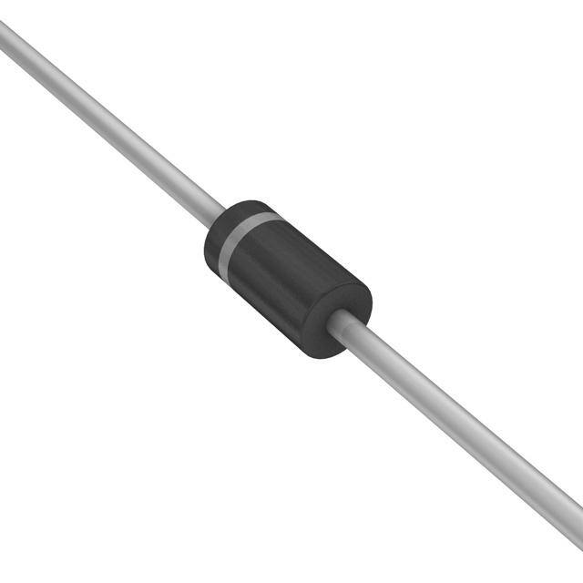
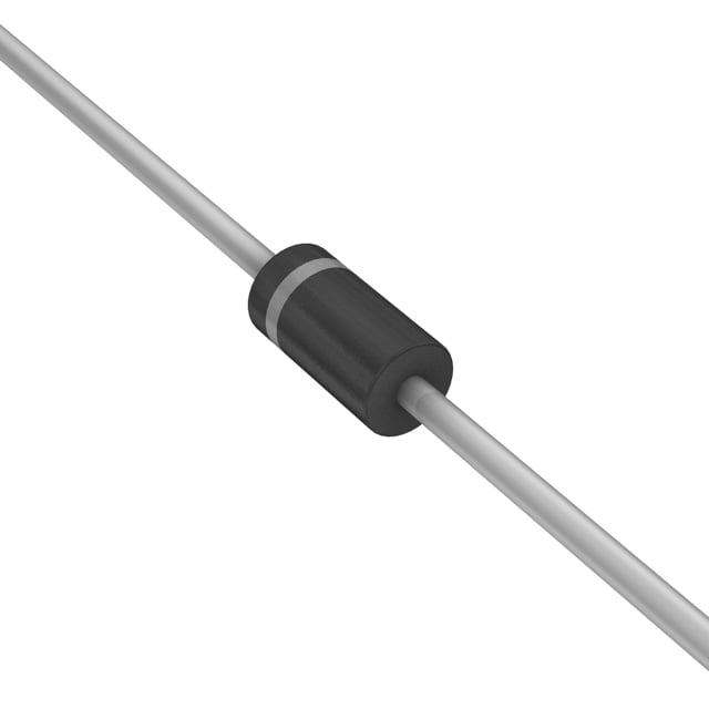
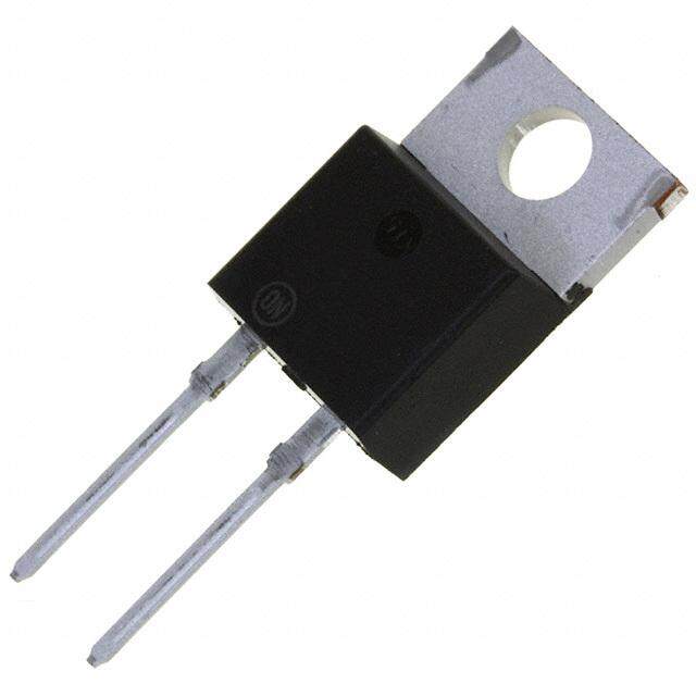
| 产品图片 |
|
| rohs | 符合RoHS无铅 / 符合限制有害物质指令(RoHS)规范要求 |
| 产品系列 | 二极管与整流器,整流器,ON Semiconductor MUR140GSWITCHMODE™ |
| 数据手册 | |
| 产品型号 | MUR140G |
| 不同If时的电压-正向(Vf) | 1.25V @ 1A |
| 不同 Vr、F时的电容 | - |
| 不同 Vr时的电流-反向漏电流 | 5µA @ 400V |
| 二极管类型 | 标准 |
| 产品 | Ultra Fast Recovery Rectifiers |
| 产品种类 | 整流器 |
| 供应商器件封装 | 轴向 |
| 其它名称 | MUR140G-ND |
| 包装 | 散装 |
| 反向恢复时间(trr) | 75ns |
| 反向电压 | 400 V |
| 反向电流IR | 5 uA |
| 商标 | ON Semiconductor |
| 安装类型 | 通孔 |
| 安装风格 | Through Hole |
| 封装 | Bulk |
| 封装/外壳 | DO-204AL,DO-41,轴向 |
| 封装/箱体 | DO-41 |
| 工作温度-结 | -65°C ~ 175°C |
| 工厂包装数量 | 1000 |
| 恢复时间 | 75 ns |
| 最大工作温度 | + 175 C |
| 最大浪涌电流 | 35 A |
| 最小工作温度 | - 65 C |
| 标准包装 | 1,000 |
| 正向电压下降 | 1.25 V |
| 正向连续电流 | 1 A |
| 热阻 | 72°C/W Ja |
| 电压-DC反向(Vr)(最大值) | 400V |
| 电流-平均整流(Io) | 1A |
| 系列 | MUR140 |
| 速度 | 快速恢复 =< 500 ns,> 200mA(Io) |
| 配置 | Single |


PDF Datasheet 数据手册内容提取
MUR120 Series SWITCHMODE Power Rectifiers MUR105, MUR110, MUR115, MUR120, MUR130, MUR140, MUR160 http://onsemi.com The MUR120 series of SWITCHMODE power rectifiers are designed for use in switching power supplies, inverters and as free ULTRAFAST RECTIFIERS wheeling diodes. 1.0 AMPERE, 50 − 600 VOLTS Features • Ultrafast 25, 50 and 75 Nanosecond Recovery Times • 175°C Operating Junction Temperature • Low Forward Voltage • Low Leakage Current • High Temperature Glass Passivated Junction • Reverse Voltage to 600 V • Shipped in Plastic Bags; 1,000 per Bag • Available Tape and Reel; 5,000 per Reel, by adding a “RL’’ Suffix to the Part Number • These are Pb−Free Devices* Mechanical Characteristics: • Case: Epoxy, Molded AXIAL LEAD • CASE 59 Weight: 0.4 Gram (Approximately) STYLE 1 • Finish: All External Surfaces Corrosion Resistant and Terminal Leads are Readily Solderable • Lead Temperature for Soldering Purposes: 260°C Max. for 10 Seconds MARKING DIAGRAM • Polarity: Cathode Indicated by Polarity Band A MUR 1xx YYWW(cid:2) (cid:2) A = Assembly Location MUR1xx= Specific Device Code Y = Year WW = Work Week (cid:2) = Pb−Free Package (Note: Microdot may be in either location) ORDERING INFORMATION See detailed ordering and shipping information in the package dimensions section on page 6 of this data sheet. *For additional information on our Pb−Free strategy and soldering details, please download the ON Semiconductor Soldering and Mounting Techniques Reference Manual, SOLDERRM/D. © Semiconductor Components Industries, LLC, 2013 1 Publication Order Number: May, 2013 − Rev. 12 MUR120/D
MUR120 Series MAXIMUM RATINGS MUR Rating Symbol 105 110 115 120 130 140 160 Unit Peak Repetitive Reverse Voltage VRRM 50 100 150 200 300 400 600 V Working Peak Reverse Voltage VRWM DC Blocking Voltage VR Average Rectified Forward Current IF(AV) 1.0 @ TA = 130°C 1.0 @ TA = 120°C A (Square Wave Mounting Method #3 Per Note 2) Nonrepetitive Peak Surge Current IFSM 35 A (Surge applied at rated load conditions, halfwave, single phase, 60 Hz) Operating Junction Temperature and Storage Temperature TJ, Tstg (cid:2)65 to +175 °C Stresses exceeding Maximum Ratings may damage the device. Maximum Ratings are stress ratings only. Functional operation above the Recommended Operating Conditions is not implied. Extended exposure to stresses above the Recommended Operating Conditions may affect device reliability. THERMAL CHARACTERISTICS Characteristic Symbol Max Unit Maximum Thermal Resistance, Junction−to−Ambient R(cid:2)JA Note 2 °C/W ELECTRICAL CHARACTERISTICS Characteristic Symbol Value Unit Maximum Instantaneous Forward Voltage (Note 1) vF V (iF = 1.0 Amp, TJ = 150°C) 0.710 1.05 (iF = 1.0 Amp, TJ = 25°C) 0.875 1.25 Maximum Instantaneous Reverse Current (Note 1) iR (cid:3)A (Rated DC Voltage, TJ = 150°C) 50 150 (Rated DC Voltage, TJ = 25°C) 2.0 5.0 Maximum Reverse Recovery Time trr ns (IF = 1.0 A, di/dt = 50 A/(cid:3)s) 35 75 (IF = 0.5 A, iR = 1.0 A, IREC = 0.25 A) 25 50 Maximum Forward Recovery Time tfr 25 50 ns (IF = 1.0 A, di/dt = 100 A/(cid:3)s, IREC to 1.0 V) Typical Peak Reverse Recovery Current IRM 0.85 A (IF = 1.0 A, di/dt = 50 A/(cid:3)s) 1. Pulse Test: Pulse Width = 300 (cid:3)s, Duty Cycle ≤2.0%. http://onsemi.com 2
MUR120 Series MUR105, MUR110, MUR115, MUR120 10 100 TJ = 175°C 7.0 5.0 (cid:3)T ( A) 10 N E R UR 1.0 100°C 3.0 C TJ = 175°C 100°C RSE 2.0 E 0.1 PS) 25°C REV AM , R T ( I 0.01 25°C N 1.0 E R R CU 0.7 0.001 D 0 20 40 60 80 100 120 140 160 180 200 R WA 0.5 VR, REVERSE VOLTAGE (VOLTS) R FO Figure 2. Typical Reverse Current* S OU 0.3 * The curves shown are typical for the highest voltage device in the E N voltage grouping. Typical reverse current for lower voltage selections NTA 0.2 can be estimated from these same curves if VR is sufficiently below TA rated VR. S N , IF 0.1 S) 5.0 i P M A 0.07 NT ( 4.0 RATED VR RE R(cid:2)JA = 50°C/W 0.05 R U D C 3.0 R A 0.03 W R O 2.0 dc F 0.02 E G SQUARE WAVE A R E 1.0 V A 0.01 , V) 0.3 0.4 0.5 0.6 0.7 0.8 0.9 1.0 1.1 1.2 1.3 A F( 0 vF, INSTANTANEOUS VOLTAGE (VOLTS) I 0 50 100 150 200 250 Figure 1. Typical Forward Voltage TA, AMBIENT TEMPERATURE (°C) Figure 3. Current Derating (Mounting Method #3 Per Note 1) S) 5.0 50 T ON (WAT 4.0 TJ = 175°C (CAPACITIVE(cid:2)LOAD)IIPAKV(cid:3)20 10 30 TJ = 25°C TI SSIPA 3.0 5.0 E (pF) 20 R DI ANC E T W CI E PO 2.0 CAPA AG dc C, 10 R E 1.0 V A 7.0 , V) SQUARE WAVE A F( 0 5.0 P 0 0.5 1.0 1.5 2.0 2.5 0 10 20 30 40 50 IF(AV), AVERAGE FORWARD CURRENT (AMPS) VR, REVERSE VOLTAGE (VOLTS) Figure 4. Power Dissipation Figure 5. Typical Capacitance http://onsemi.com 3
MUR120 Series MUR130, MUR140, MUR160 10 400 7.0 100 TJ = 175°C 5.0 (cid:3)T ( A) 40 N 10 E R UR 4.0 100°C 3.0 C TJ = 175°C 100°C RSE 1.0 2.0 E 0.4 S) 25°C EV AMP , RR 0.1 25°C T ( I 0.04 N 1.0 E R 0.01 R CU 0.7 0.004 D 0 100 200 300 400 500 600 700 R WA 0.5 VR, REVERSE VOLTAGE (VOLTS) R FO Figure 7. Typical Reverse Current* S OU 0.3 * The curves shown are typical for the highest voltage device in the E N voltage grouping. Typical reverse current for lower voltage selections NTA 0.2 can be estimated from these same curves if VR is sufficiently below TA rated VR. S N , IF 0.1 S) 5.0 i P M A 0.07 NT ( 4.0 RATED VR RE R(cid:2)JA = 50°C/W 0.05 R U D C 3.0 R A 0.03 W R O 2.0 F 0.02 E dc G A R E 1.0 AV SQUARE WAVE 0.01 , V) 0.3 0.5 0.7 0.9 1.1 1.3 1.5 1.7 1.9 2.1 2.3 A F( 0 vF, INSTANTANEOUS VOLTAGE (VOLTS) I 0 50 100 150 200 250 Figure 6. Typical Forward Voltage TA, AMBIENT TEMPERATURE (°C) Figure 8. Current Derating (Mounting Method #3 Per Note 2) S) 5.0 20 T WAT TJ = 175°C ON ( 4.0 TJ = 25°C WER DISSIPATI 3.0 (CAPAICPIKTIV(cid:3)E L2O0AD) 10 5.0 dc CITANCE (pF) 71.00 E PO 2.0 IAV CAPA 5.0 AG SQUARE WAVE C, R E 1.0 AV 3.0 , V) A F( 0 2.0 P 0 0.5 1.0 1.5 2.0 2.5 0 10 20 30 40 50 IF(AV), AVERAGE FORWARD CURRENT (AMPS) VR, REVERSE VOLTAGE (VOLTS) Figure 9. Power Dissipation Figure 10. Typical Capacitance http://onsemi.com 4
MUR120 Series NOTE 2. — AMBIENT MOUNTING DATA Data shown for thermal resistance, junction−to−ambient (R(cid:2)JA) for the mountings shown is to be used as typical guideline values for preliminary engineering or in case the tie point temperature cannot be measured. TYPICAL VALUES FOR R(cid:2)JA IN STILL AIR Mounting Lead Length, L (in.) Method 1/8 1/4 1/2 Units 1 52 65 72 °C/W 2 R(cid:2)JA 67 80 87 °C/W 3 50 °C/W MOUNTING METHOD 1 L L ÉÉÉÉÉÉÉÉÉÉÉ ÉÉÉÉÉÉÉÉÉÉÉ MOUNTING METHOD 2 L L ÉÉÉÉÉÉÉÉÉÉÉÉ ÉÉÉÉÉÉÉÉÉÉÉÉ Vector Pin Mounting MOUNTING METHOD 3 ÉÉ ÉÉ L = 3/8″ ÉÉ ÉÉ ÉÉ ÉÉ Board Ground Plane ÉÉ P.C. Board with 1−1/2 ″ X 1−1/2 ″ Copper Surface http://onsemi.com 5
MUR120 Series ORDERING INFORMATION Device Marking Package Shipping† MUR105 MUR105 Axial Lead* 1000 Units / Bag MUR105G MUR105 Axial Lead* 1000 Units / Bag MUR105RL MUR105 Axial Lead* 5000 Units / Tape & Reel MUR105RLG MUR105 Axial Lead* 5000 Units / Tape & Reel MUR110 MUR110 Axial Lead* 1000 Units / Bag MUR110G MUR110 Axial Lead* 1000 Units / Bag MUR110RL MUR110 Axial Lead* 5000 Units / Tape & Reel MUR110RLG MUR110 Axial Lead* 5000 Units / Tape & Reel MUR115 MUR115 Axial Lead* 1000 Units / Bag MUR115G MUR115 Axial Lead* 1000 Units / Bag MUR115RL MUR115 Axial Lead* 5000 Units / Tape & Reel MUR115RLG MUR115 Axial Lead* 5000 Units / Tape & Reel MUR120 MUR120 Axial Lead* 1000 Units / Bag MUR120G MUR120 Axial Lead* 1000 Units / Bag MUR120RL MUR120 Axial Lead* 5000 Units / Tape & Reel MUR120RLG MUR120 Axial Lead* 5000 Units / Tape & Reel MUR130 MUR130 Axial Lead* 1000 Units / Bag MUR130G MUR130 Axial Lead* 1000 Units / Bag MUR130RL MUR130 Axial Lead* 5000 Units / Tape & Reel MUR130RLG MUR130 Axial Lead* 5000 Units / Tape & Reel MUR140 MUR140 Axial Lead* 1000 Units / Bag MUR140G MUR140 Axial Lead* 1000 Units / Bag MUR140RL MUR140 Axial Lead* 5000 Units / Tape & Reel MUR140RLG MUR140 Axial Lead* 5000 Units / Tape & Reel MUR160 MUR160 Axial Lead* 1000 Units / Bag MUR160G MUR160 Axial Lead* 1000 Units / Bag MUR160RL MUR160 Axial Lead* 5000 Units / Tape & Reel MUR160RLG MUR160 Axial Lead* 5000 Units / Tape & Reel †For information on tape and reel specifications, including part orientation and tape sizes, please refer to our Tape and Reel Packaging Specifications Brochure, BRD8011/D. *This package is inherently Pb−Free. http://onsemi.com 6
MUR120 Series PACKAGE DIMENSIONS AXIAL LEAD CASE 59−10 ISSUE U NOTES: 1. DIMENSIONING AND TOLERANCING PER ANSI B Y14.5M, 1982. 2. CONTROLLING DIMENSION: INCH. 3. ALL RULES AND NOTES ASSOCIATED WITH JEDEC DO−41 OUTLINE SHALL APPLY 4. POLARITY DENOTED BY CATHODE BAND. 5. LEAD DIAMETER NOT CONTROLLED WITHIN F DIMENSION. K D INCHES MILLIMETERS DIM MIN MAX MIN MAX F A 0.161 0.205 4.10 5.20 B 0.079 0.106 2.00 2.70 D 0.028 0.034 0.71 0.86 A F −−− 0.050 −−− 1.27 K 1.000 −−− 25.40 −−− POLARITY INDICATOR OPTIONAL AS NEEDED F STYLE 1: (SEE STYLES) PIN 1.CATHODE (POLARITY BAND) 2.ANODE K ON Semiconductor and are registered trademarks of Semiconductor Components Industries, LLC (SCILLC). SCILLC owns the rights to a number of patents, trademarks, copyrights, trade secrets, and other intellectual property. A listing of SCILLC’s product/patent coverage may be accessed at www.onsemi.com/site/pdf/Patent−Marking.pdf. SCILLC reserves the right to make changes without further notice to any products herein. SCILLC makes no warranty, representation or guarantee regarding the suitability of its products for any particular purpose, nor does SCILLC assume any liability arising out of the application or use of any product or circuit, and specifically disclaims any and all liability, including without limitation special, consequential or incidental damages. “Typical” parameters which may be provided in SCILLC data sheets and/or specifications can and do vary in different applications and actual performance may vary over time. All operating parameters, including “Typicals” must be validated for each customer application by customer’s technical experts. SCILLC does not convey any license under its patent rights nor the rights of others. SCILLC products are not designed, intended, or authorized for use as components in systems intended for surgical implant into the body, or other applications intended to support or sustain life, or for any other application in which the failure of the SCILLC product could create a situation where personal injury or death may occur. Should Buyer purchase or use SCILLC products for any such unintended or unauthorized application, Buyer shall indemnify and hold SCILLC and its officers, employees, subsidiaries, affiliates, and distributors harmless against all claims, costs, damages, and expenses, and reasonable attorney fees arising out of, directly or indirectly, any claim of personal injury or death associated with such unintended or unauthorized use, even if such claim alleges that SCILLC was negligent regarding the design or manufacture of the part. SCILLC is an Equal Opportunity/Affirmative Action Employer. This literature is subject to all applicable copyright laws and is not for resale in any manner. PUBLICATION ORDERING INFORMATION LITERATURE FULFILLMENT: N. American Technical Support: 800−282−9855 Toll Free ON Semiconductor Website: www.onsemi.com Literature Distribution Center for ON Semiconductor USA/Canada P.O. Box 5163, Denver, Colorado 80217 USA Europe, Middle East and Africa Technical Support: Order Literature: http://www.onsemi.com/orderlit Phone: 303−675−2175 or 800−344−3860 Toll Free USA/Canada Phone: 421 33 790 2910 Fax: 303−675−2176 or 800−344−3867 Toll Free USA/Canada Japan Customer Focus Center For additional information, please contact your local Email: orderlit@onsemi.com Phone: 81−3−5817−1050 Sales Representative http://onsemi.com MUR120/D 7
Mouser Electronics Authorized Distributor Click to View Pricing, Inventory, Delivery & Lifecycle Information: O N Semiconductor: MUR105G MUR105RLG MUR110G MUR110RLG MUR115G MUR115RLG MUR120G MUR120RLG MUR130G MUR130RLG MUR140G MUR140RLG MUR160G MUR160RLG