 Datasheet下载
- 型号: MT46V16M16CY-5B:K TR
- 制造商: Micron Technology Inc
- 库位|库存: xxxx|xxxx
- 要求:
| 数量阶梯 | 香港交货 | 国内含税 |
| +xxxx | $xxxx | ¥xxxx |
查看当月历史价格
查看今年历史价格
MT46V16M16CY-5B:K TR产品简介:
ICGOO电子元器件商城为您提供MT46V16M16CY-5B:K TR由Micron Technology Inc设计生产,在icgoo商城现货销售,并且可以通过原厂、代理商等渠道进行代购。 MT46V16M16CY-5B:K TR价格参考。Micron Technology IncMT46V16M16CY-5B:K TR封装/规格:存储器, SDRAM - DDR 存储器 IC 256Mb (16M x 16) 并联 200MHz 700ps 60-FBGA(8x12.5)。您可以下载MT46V16M16CY-5B:K TR参考资料、Datasheet数据手册功能说明书,资料中有MT46V16M16CY-5B:K TR 详细功能的应用电路图电压和使用方法及教程。
Micron Technology Inc. 的存储器产品 MT46V16M16CY-5B:K TR 是一款高性能的DRAM(动态随机存取存储器)芯片,主要应用于需要高速数据处理和大容量内存的电子设备中。

该型号存储器常用于网络设备、服务器、工业控制设备以及高端消费类电子产品。其高带宽和低延迟特性使其非常适合用于路由器、交换机等通信基础设施中,以支持快速的数据转发和处理。此外,它也可用于图像处理设备、嵌入式系统和自动化控制系统,为这些应用提供稳定可靠的内存支持。

由于其工业级的设计和稳定性,MT46V16M16CY-5B:K TR 也广泛应用于对可靠性要求较高的工业和车载系统中。例如,在智能交通系统、视频监控设备以及自动化生产线中,该存储器可确保设备在复杂环境下稳定运行。

总之,这款存储器适用于各类对性能与稳定性有较高要求的电子系统,是现代高性能计算和数据密集型应用的理想选择。
| 参数 | 数值 |
| 产品目录 | 集成电路 (IC) |
| 描述 | IC DDR SDRAM 256MBIT 5NS 60FBGA |
| 产品分类 | |
| 品牌 | Micron Technology Inc |
| 数据手册 | |
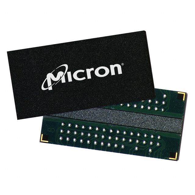
| 产品图片 |
|
| 产品型号 | MT46V16M16CY-5B:K TR |
| PCN过时产品 | |
| rohs | 无铅 / 符合限制有害物质指令(RoHS)规范要求 |
| 产品系列 | - |
| 产品目录页面 | |
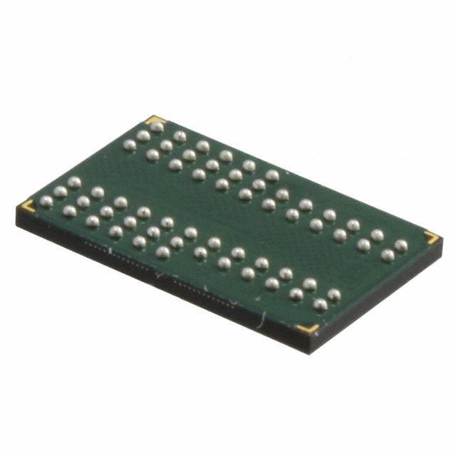
| 供应商器件封装 | 60-FBGA(8x12.5) |
| 其它名称 | 557-1445-6 |
| 包装 | Digi-Reel® |
| 存储器类型 | DDR SDRAM |
| 存储容量 | 256M (16M x 16) |
| 封装/外壳 | 60-TFBGA |
| 工作温度 | 0°C ~ 70°C |
| 接口 | 并联 |
| 标准包装 | 1 |
| 格式-存储器 | RAM |
| 电压-电源 | 2.5 V ~ 2.7 V |
| 速度 | 5ns |


_renders/IS42S32800J-6TLI.jpg)

_renders/MR4A16BCYS35.jpg)

- 商务部:美国ITC正式对集成电路等产品启动337调查
- 曝三星4nm工艺存在良率问题 高通将骁龙8 Gen1或转产台积电
- 太阳诱电将投资9.5亿元在常州建新厂生产MLCC 预计2023年完工
- 英特尔发布欧洲新工厂建设计划 深化IDM 2.0 战略
- 台积电先进制程称霸业界 有大客户加持明年业绩稳了
- 达到5530亿美元!SIA预计今年全球半导体销售额将创下新高
- 英特尔拟将自动驾驶子公司Mobileye上市 估值或超500亿美元
- 三星加码芯片和SET,合并消费电子和移动部门,撤换高东真等 CEO
- 三星电子宣布重大人事变动 还合并消费电子和移动部门
- 海关总署:前11个月进口集成电路产品价值2.52万亿元 增长14.8%

_renders/IS42S32800D-6BLI.jpg)

PDF Datasheet 数据手册内容提取
256Mb: x4, x8, x16 DDR SDRAM Features Double Data Rate (DDR) SDRAM MT46V64M4 – 16 Meg x 4 x 4 banks MT46V32M8 – 8 Meg x 8 x 4 banks MT46V16M16 – 4 Meg x 16 x 4 banks Features Options Marking • VDD = 2.5V ±0.2V; VDDQ = 2.5V ±0.2V • Configuration VDD = 2.6V ±0.1V; VDDQ = 2.6V ±0.1V (DDR400)1 – 64 Meg x 4 (16 Meg x 4 x 4 banks) 64M4 • Bidirectional data strobe (DQS) transmitted/ – 32 Meg x 8 (8 Meg x 8 x 4 banks) 32M8 received with data, that is, source-synchronous data – 16 Meg x 16 (4 Meg x 16 x 4 banks) 16M16 capture (x16 has two – one per byte) • Plastic package – OCPL • Internal, pipelined double data rate (DDR) – 66-pin TSOP TG architecture; two data accesses per clock cycle – 66-pin TSOP (Pb-free) P • Differential clock inputs (CK and CK#) • Plastic package • Commands entered on each positive CK edge – 60-ball FBGA (8mm x 12.5mm) CV • DQS edge-aligned with data for READs; center- – 60-ball FBGA (8mm x 12.5mm) CY aligned with data for WRITEs (Pb-free) • DLL to align DQ and DQS transitions with CK • Timing – cycle time • Four internal banks for concurrent operation – 5ns @ CL = 3 (DDR400) -5B3 • Data mask (DM) for masking write data – 6ns @ CL = 2.5 (DDR333) FBGA only -62 (x16 has two – one per byte) – 6ns @ CL = 2.5 (DDR333) TSOP only -6T2 • Programmable burst lengths (BL): 2, 4, or 8 • Self refresh • Auto refresh – Standard None – 64ms, 8192-cycle – Low-power self refresh L • Longer-lead TSOP for improved reliability (OCPL) • Temperature rating • 2.5V I/O (SSTL_2-compatible) – Commercial (0(cid:113)C to +70(cid:113)C) None • Concurrent auto precharge option supported – Industrial (–40(cid:113)C to +85(cid:113)C) IT • tRAS lockout supported (tRAP = tRCD) • Revision – x4, x8, x16 :K4 – x4, x8, x16 :M Notes:1. DDR400 devices operating at < DDR333 conditions can use V /V = 2.5V +0.2V. DD DDQ 2. Available only on Revision K. 3. Available only on Revision M. 4. Not recommended for new designs. Table 1: Key Timing Parameters CL = CAS (READ) latency; MIN clock rate with 50% duty cycle at CL = 2 (-75E, -75Z), CL = 2.5 (-6, -6T, -75), and CL = 3 (-5B) Clock Rate (MHz) Access DQS–DQ Speed Grade CL = 2 CL = 2.5 CL = 3 Data-Out Window Window Skew -5B 133 167 200 1.6ns ±0.70ns 0.40ns -6 133 167 n/a 2.1ns ±0.70ns 0.40ns 6T 133 167 n/a 2.0ns ±0.70ns 0.45ns -75E/-75Z 133 133 n/a 2.5ns ±0.75ns 0.50ns -75 100 133 n/a 2.5ns ±0.75ns 0.50ns PDF: 09005aef80768abb/Source: 09005aef82a95a3a 1 Micron Technology, Inc., reserves the right to change products or specifications without notice. 256Mb_DDR_x4x8x16_D1.fm-256Mb DDR: Rev. S, Core DDR: Rev. E 3/15 EN ©2003 Micron Technology, Inc. All rights reserved. Products and specifications discussed herein are subject to change by Micron without notice.
256Mb: x4, x8, x16 DDR SDRAM Features Table 2: Addressing Parameter 64 Meg x 4 32 Meg x 8 16 Meg x 16 Configuration 16 Meg x 4 x 4 banks 8 Meg x 8 x 4 banks 4 Meg x 16 x 4 banks Refresh count 8K 8K 8K Row address 8K (A[12:0]) 8K (A[12:0]) 8K (A[12:0]) Bank address 4 (BA[1:0]) 4 (BA[1:0]) 4 (BA[1:0]) Column address 2K (A[9:0], A11) 1K (A[9:0]) 512 (A[8:0]) Table 3: Speed Grade Compatibility Marking PC3200 (3-3-3) PC2700 (2.5-3-3) PC2100 (2-2-2) PC2100 (2-3-3) PC2100 (2.5-3-3) PC1600(2-2-2) -5B1 Yes Yes Yes Yes Yes Yes -6 – Yes Yes Yes Yes Yes -6T – Yes Yes Yes Yes Yes -75E – – Yes Yes Yes Yes -75Z – – – Yes Yes Yes -75 – – – – Yes Yes -5B -6/-6T -75E -75Z -75 -75 Notes: 1. The -5B device is backward compatible with all slower speed grades. The voltage range of -5B device operating at slower speed grades is V = V = 2.5V ± 0.2V. DD DDQ Figure 1: 256Mb DDR SDRAM Part Numbers Example Part Number: MT46V16M16P-6T:M - : Sp. MT46V Configuration Package Speed Op. Temp.Revision Configuration Revision 64 Meg x 4 64M4 :K x4, x8, x16 32 Meg x 8 32M8 :M x4, x8, x16 16 Meg x 16 16M16 Package Operating Temp. 400-mil TSOP TG Commercial 400-mil TSOP (Pb-free) P IT Industrial 8mm x 12.5mm FBGA CV 8mm x 12.5mm FBGA (Pb-free) CY Special Options Standard L Low power Speed Grade t -5B CK = 5ns, CL = 3 t -6 CK = 6ns, CL = 2.5 t -6T CK = 6ns, CL = 2.5 PDF: 09005aef80768abb/Source: 09005aef82a95a3a 2 Micron Technology, Inc., reserves the right to change products or specifications without notice. 256Mb_DDR_x4x8x16_D1.fm-256Mb DDR: Rev. S, Core DDR: Rev. E 3/15 EN ©2003 Micron Technology, Inc. All rights reserved.
256Mb: x4, x8, x16 DDR SDRAM Features FBGA Part Marking System Due to space limitations, FBGA-packaged components have an abbreviated part marking that is different from the part number. For a quick conversion of an FBGA code, see the FBGA Part Marking Decoder on Micron’s Web site: www.micron.com. PDF: 09005aef80768abb/Source: 09005aef82a95a3a 3 Micron Technology, Inc., reserves the right to change products or specifications without notice. 256Mb_DDR_x4x8x16_D1.fm-256Mb DDR: Rev. S, Core DDR: Rev. E 3/15 EN ©2003 Micron Technology, Inc. All rights reserved.
256Mb: x4, x8, x16 DDR SDRAM Table of Contents Table of Contents Features. . . . . . . . . . . . . . . . . . . . . . . . . . . . . . . . . . . . . . . . . . . . . . . . . . . . . . . . . . . . . . . . . . . . . . . . . . . . . . . . . . . . . . . . . . . . . .1 State Diagram. . . . . . . . . . . . . . . . . . . . . . . . . . . . . . . . . . . . . . . . . . . . . . . . . . . . . . . . . . . . . . . . . . . . . . . . . . . . . . . . . . . . . . . . .7 Functional Description . . . . . . . . . . . . . . . . . . . . . . . . . . . . . . . . . . . . . . . . . . . . . . . . . . . . . . . . . . . . . . . . . . . . . . . . . . . . . . . .8 General Notes . . . . . . . . . . . . . . . . . . . . . . . . . . . . . . . . . . . . . . . . . . . . . . . . . . . . . . . . . . . . . . . . . . . . . . . . . . . . . . . . . . . . . .8 Functional Block Diagrams. . . . . . . . . . . . . . . . . . . . . . . . . . . . . . . . . . . . . . . . . . . . . . . . . . . . . . . . . . . . . . . . . . . . . . . . . . . . .9 Pin and Ball Assignments and Descriptions . . . . . . . . . . . . . . . . . . . . . . . . . . . . . . . . . . . . . . . . . . . . . . . . . . . . . . . . . . . . .11 Package Dimensions . . . . . . . . . . . . . . . . . . . . . . . . . . . . . . . . . . . . . . . . . . . . . . . . . . . . . . . . . . . . . . . . . . . . . . . . . . . . . . . . .14 Electrical Specifications – IDD. . . . . . . . . . . . . . . . . . . . . . . . . . . . . . . . . . . . . . . . . . . . . . . . . . . . . . . . . . . . . . . . . . . . . . . . .16 Electrical Specifications – DC and AC. . . . . . . . . . . . . . . . . . . . . . . . . . . . . . . . . . . . . . . . . . . . . . . . . . . . . . . . . . . . . . . . . . .18 Notes. . . . . . . . . . . . . . . . . . . . . . . . . . . . . . . . . . . . . . . . . . . . . . . . . . . . . . . . . . . . . . . . . . . . . . . . . . . . . . . . . . . . . . . . . . . . .35 Commands. . . . . . . . . . . . . . . . . . . . . . . . . . . . . . . . . . . . . . . . . . . . . . . . . . . . . . . . . . . . . . . . . . . . . . . . . . . . . . . . . . . . . . . . . .43 DESELECT . . . . . . . . . . . . . . . . . . . . . . . . . . . . . . . . . . . . . . . . . . . . . . . . . . . . . . . . . . . . . . . . . . . . . . . . . . . . . . . . . . . . . . . .47 NO OPERATION (NOP). . . . . . . . . . . . . . . . . . . . . . . . . . . . . . . . . . . . . . . . . . . . . . . . . . . . . . . . . . . . . . . . . . . . . . . . . . . . .47 LOAD MODE REGISTER (LMR) . . . . . . . . . . . . . . . . . . . . . . . . . . . . . . . . . . . . . . . . . . . . . . . . . . . . . . . . . . . . . . . . . . . . .47 ACTIVE (ACT) . . . . . . . . . . . . . . . . . . . . . . . . . . . . . . . . . . . . . . . . . . . . . . . . . . . . . . . . . . . . . . . . . . . . . . . . . . . . . . . . . . . . .48 READ. . . . . . . . . . . . . . . . . . . . . . . . . . . . . . . . . . . . . . . . . . . . . . . . . . . . . . . . . . . . . . . . . . . . . . . . . . . . . . . . . . . . . . . . . . . . .49 WRITE. . . . . . . . . . . . . . . . . . . . . . . . . . . . . . . . . . . . . . . . . . . . . . . . . . . . . . . . . . . . . . . . . . . . . . . . . . . . . . . . . . . . . . . . . . . .50 PRECHARGE (PRE) . . . . . . . . . . . . . . . . . . . . . . . . . . . . . . . . . . . . . . . . . . . . . . . . . . . . . . . . . . . . . . . . . . . . . . . . . . . . . . . .51 BURST TERMINATE (BST). . . . . . . . . . . . . . . . . . . . . . . . . . . . . . . . . . . . . . . . . . . . . . . . . . . . . . . . . . . . . . . . . . . . . . . . . .51 AUTO REFRESH (AR). . . . . . . . . . . . . . . . . . . . . . . . . . . . . . . . . . . . . . . . . . . . . . . . . . . . . . . . . . . . . . . . . . . . . . . . . . . . . . .51 SELF REFRESH . . . . . . . . . . . . . . . . . . . . . . . . . . . . . . . . . . . . . . . . . . . . . . . . . . . . . . . . . . . . . . . . . . . . . . . . . . . . . . . . . . . .51 Operations . . . . . . . . . . . . . . . . . . . . . . . . . . . . . . . . . . . . . . . . . . . . . . . . . . . . . . . . . . . . . . . . . . . . . . . . . . . . . . . . . . . . . . . . . .52 INITIALIZATION . . . . . . . . . . . . . . . . . . . . . . . . . . . . . . . . . . . . . . . . . . . . . . . . . . . . . . . . . . . . . . . . . . . . . . . . . . . . . . . . . .52 REGISTER DEFINITION. . . . . . . . . . . . . . . . . . . . . . . . . . . . . . . . . . . . . . . . . . . . . . . . . . . . . . . . . . . . . . . . . . . . . . . . . . . .55 ACTIVE . . . . . . . . . . . . . . . . . . . . . . . . . . . . . . . . . . . . . . . . . . . . . . . . . . . . . . . . . . . . . . . . . . . . . . . . . . . . . . . . . . . . . . . . . . .59 READ. . . . . . . . . . . . . . . . . . . . . . . . . . . . . . . . . . . . . . . . . . . . . . . . . . . . . . . . . . . . . . . . . . . . . . . . . . . . . . . . . . . . . . . . . . . . .60 WRITE. . . . . . . . . . . . . . . . . . . . . . . . . . . . . . . . . . . . . . . . . . . . . . . . . . . . . . . . . . . . . . . . . . . . . . . . . . . . . . . . . . . . . . . . . . . .72 PRECHARGE . . . . . . . . . . . . . . . . . . . . . . . . . . . . . . . . . . . . . . . . . . . . . . . . . . . . . . . . . . . . . . . . . . . . . . . . . . . . . . . . . . . . . .85 AUTO REFRESH . . . . . . . . . . . . . . . . . . . . . . . . . . . . . . . . . . . . . . . . . . . . . . . . . . . . . . . . . . . . . . . . . . . . . . . . . . . . . . . . . . .87 SELF REFRESH . . . . . . . . . . . . . . . . . . . . . . . . . . . . . . . . . . . . . . . . . . . . . . . . . . . . . . . . . . . . . . . . . . . . . . . . . . . . . . . . . . . .88 Power-down (CKE Not Active) . . . . . . . . . . . . . . . . . . . . . . . . . . . . . . . . . . . . . . . . . . . . . . . . . . . . . . . . . . . . . . . . . . . . . .90 PDF: 09005aef80768abb/Source: 09005aef82a95a3a 4 Micron Technology, Inc., reserves the right to change products or specifications without notice. 256Mb_DDRTOC.fm-256Mb DDR: Rev. S, Core DDR: Rev. E 3/15 EN ©2003 Micron Technology, Inc. All rights reserved.
256Mb: x4, x8, x16 DDR SDRAM List of Figures List of Figures Figure 1: 256Mb DDR SDRAM Part Numbers . . . . . . . . . . . . . . . . . . . . . . . . . . . . . . . . . . . . . . . . . . . . . . . . . . . . . . . . .2 Figure 2: Simplified State Diagram . . . . . . . . . . . . . . . . . . . . . . . . . . . . . . . . . . . . . . . . . . . . . . . . . . . . . . . . . . . . . . . . . .7 Figure 6: 66-Pin TSOP Pin Assignments (Top View) . . . . . . . . . . . . . . . . . . . . . . . . . . . . . . . . . . . . . . . . . . . . . . . . . .11 Figure 8: 66-Pin Plastic TSOP (400 mil). . . . . . . . . . . . . . . . . . . . . . . . . . . . . . . . . . . . . . . . . . . . . . . . . . . . . . . . . . . . . .14 Figure 9: 60-Ball FBGA (8mm x 12.5mm) . . . . . . . . . . . . . . . . . . . . . . . . . . . . . . . . . . . . . . . . . . . . . . . . . . . . . . . . . . . .15 Figure 10: Input Voltage Waveform. . . . . . . . . . . . . . . . . . . . . . . . . . . . . . . . . . . . . . . . . . . . . . . . . . . . . . . . . . . . . . . . . .20 Figure 11: SSTL_2 Clock Input . . . . . . . . . . . . . . . . . . . . . . . . . . . . . . . . . . . . . . . . . . . . . . . . . . . . . . . . . . . . . . . . . . . . . .21 Figure 12: Derating Data Valid Window (tQH – tDQSQ) . . . . . . . . . . . . . . . . . . . . . . . . . . . . . . . . . . . . . . . . . . . . . . . .37 Figure 13: Full Drive Pull-Down Characteristics. . . . . . . . . . . . . . . . . . . . . . . . . . . . . . . . . . . . . . . . . . . . . . . . . . . . . . .38 Figure 14: Full Drive Pull-Up Characteristics . . . . . . . . . . . . . . . . . . . . . . . . . . . . . . . . . . . . . . . . . . . . . . . . . . . . . . . . .38 Figure 15: Reduced Drive Pull-Down Characteristics . . . . . . . . . . . . . . . . . . . . . . . . . . . . . . . . . . . . . . . . . . . . . . . . . .39 Figure 16: Reduced Drive Pull-Up Characteristics. . . . . . . . . . . . . . . . . . . . . . . . . . . . . . . . . . . . . . . . . . . . . . . . . . . . .39 Figure 17: Activating a Specific Row in a Specific Bank. . . . . . . . . . . . . . . . . . . . . . . . . . . . . . . . . . . . . . . . . . . . . . . . .48 Figure 18: READ Command. . . . . . . . . . . . . . . . . . . . . . . . . . . . . . . . . . . . . . . . . . . . . . . . . . . . . . . . . . . . . . . . . . . . . . . . .49 Figure 19: WRITE Command. . . . . . . . . . . . . . . . . . . . . . . . . . . . . . . . . . . . . . . . . . . . . . . . . . . . . . . . . . . . . . . . . . . . . . . .50 Figure 20: PRECHARGE Command. . . . . . . . . . . . . . . . . . . . . . . . . . . . . . . . . . . . . . . . . . . . . . . . . . . . . . . . . . . . . . . . . .51 Figure 21: INITIALIZATION Flow Diagram . . . . . . . . . . . . . . . . . . . . . . . . . . . . . . . . . . . . . . . . . . . . . . . . . . . . . . . . . . .53 Figure 22: INITIALIZATION Timing Diagram . . . . . . . . . . . . . . . . . . . . . . . . . . . . . . . . . . . . . . . . . . . . . . . . . . . . . . . . .54 Figure 23: Mode Register Definition . . . . . . . . . . . . . . . . . . . . . . . . . . . . . . . . . . . . . . . . . . . . . . . . . . . . . . . . . . . . . . . . .55 Figure 24: CAS Latency. . . . . . . . . . . . . . . . . . . . . . . . . . . . . . . . . . . . . . . . . . . . . . . . . . . . . . . . . . . . . . . . . . . . . . . . . . . . .57 Figure 25: Extended Mode Register Definition . . . . . . . . . . . . . . . . . . . . . . . . . . . . . . . . . . . . . . . . . . . . . . . . . . . . . . . .59 Figure 26: Example: Meeting tRCD (tRRD) MIN When 2 < tRCD (tRRD) MIN/tCK (cid:100)(cid:3)3. . . . . . . . . . . . . . . . . . . . . .60 Figure 29: Nonconsecutive READ Bursts . . . . . . . . . . . . . . . . . . . . . . . . . . . . . . . . . . . . . . . . . . . . . . . . . . . . . . . . . . . . .64 Figure 30: Random READ Accesses . . . . . . . . . . . . . . . . . . . . . . . . . . . . . . . . . . . . . . . . . . . . . . . . . . . . . . . . . . . . . . . . . .65 Figure 31: Terminating a READ Burst . . . . . . . . . . . . . . . . . . . . . . . . . . . . . . . . . . . . . . . . . . . . . . . . . . . . . . . . . . . . . . . .66 Figure 32: READ-to-WRITE . . . . . . . . . . . . . . . . . . . . . . . . . . . . . . . . . . . . . . . . . . . . . . . . . . . . . . . . . . . . . . . . . . . . . . . . .67 Figure 33: READ-to-PRECHARGE . . . . . . . . . . . . . . . . . . . . . . . . . . . . . . . . . . . . . . . . . . . . . . . . . . . . . . . . . . . . . . . . . . .68 Figure 34: Bank READ – Without Auto Precharge. . . . . . . . . . . . . . . . . . . . . . . . . . . . . . . . . . . . . . . . . . . . . . . . . . . . . .69 Figure 35: x4, x8 Data Output Timing – tDQSQ, tQH, and Data Valid Window . . . . . . . . . . . . . . . . . . . . . . . . . . . .70 Figure 36: x16 Data Output Timing – tDQSQ, tQH, and Data Valid Window . . . . . . . . . . . . . . . . . . . . . . . . . . . . . .71 Figure 37: Data Output Timing – tAC and tDQSCK. . . . . . . . . . . . . . . . . . . . . . . . . . . . . . . . . . . . . . . . . . . . . . . . . . . . .72 Figure 38: WRITE Burst. . . . . . . . . . . . . . . . . . . . . . . . . . . . . . . . . . . . . . . . . . . . . . . . . . . . . . . . . . . . . . . . . . . . . . . . . . . . .74 Figure 39: Consecutive WRITE-to-WRITE . . . . . . . . . . . . . . . . . . . . . . . . . . . . . . . . . . . . . . . . . . . . . . . . . . . . . . . . . . . .75 Figure 41: Random WRITE Cycles . . . . . . . . . . . . . . . . . . . . . . . . . . . . . . . . . . . . . . . . . . . . . . . . . . . . . . . . . . . . . . . . . . .76 Figure 42: WRITE-to-READ – Uninterrupting . . . . . . . . . . . . . . . . . . . . . . . . . . . . . . . . . . . . . . . . . . . . . . . . . . . . . . . . .77 Figure 43: WRITE-to-READ – Interrupting. . . . . . . . . . . . . . . . . . . . . . . . . . . . . . . . . . . . . . . . . . . . . . . . . . . . . . . . . . . .78 Figure 44: WRITE-to-READ – Odd Number of Data, Interrupting . . . . . . . . . . . . . . . . . . . . . . . . . . . . . . . . . . . . . . .79 Figure 45: WRITE-to-PRECHARGE – Uninterrupting . . . . . . . . . . . . . . . . . . . . . . . . . . . . . . . . . . . . . . . . . . . . . . . . . .80 Figure 46: WRITE-to-PRECHARGE – Interrupting . . . . . . . . . . . . . . . . . . . . . . . . . . . . . . . . . . . . . . . . . . . . . . . . . . . . .81 Figure 47: WRITE-to-PRECHARGE – Odd Number of Data, Interrupting. . . . . . . . . . . . . . . . . . . . . . . . . . . . . . . . .82 Figure 48: Bank WRITE – Without Auto Precharge. . . . . . . . . . . . . . . . . . . . . . . . . . . . . . . . . . . . . . . . . . . . . . . . . . . . .83 Figure 49: WRITE – DM Operation. . . . . . . . . . . . . . . . . . . . . . . . . . . . . . . . . . . . . . . . . . . . . . . . . . . . . . . . . . . . . . . . . . .84 Figure 50: Data Input Timing . . . . . . . . . . . . . . . . . . . . . . . . . . . . . . . . . . . . . . . . . . . . . . . . . . . . . . . . . . . . . . . . . . . . . . .85 Figure 51: Bank READ – with Auto Precharge . . . . . . . . . . . . . . . . . . . . . . . . . . . . . . . . . . . . . . . . . . . . . . . . . . . . . . . . .86 Figure 52: Bank WRITE – with Auto Precharge . . . . . . . . . . . . . . . . . . . . . . . . . . . . . . . . . . . . . . . . . . . . . . . . . . . . . . . .87 Figure 53: Auto Refresh Mode. . . . . . . . . . . . . . . . . . . . . . . . . . . . . . . . . . . . . . . . . . . . . . . . . . . . . . . . . . . . . . . . . . . . . . .88 Figure 54: Self Refresh Mode. . . . . . . . . . . . . . . . . . . . . . . . . . . . . . . . . . . . . . . . . . . . . . . . . . . . . . . . . . . . . . . . . . . . . . . .89 PDF: 09005aef80768abb/Source: 09005aef82a95a3a 5 Micron Technology, Inc., reserves the right to change products or specifications without notice. 256Mb_DDRLOF.fm-256Mb DDR: Rev. S, Core DDR: Rev. E 3/15 EN ©2003 Micron Technology, Inc. All rights reserved.
256Mb: x4, x8, x16 DDR SDRAM List of Tables List of Tables Table 1: Key Timing Parameters. . . . . . . . . . . . . . . . . . . . . . . . . . . . . . . . . . . . . . . . . . . . . . . . . . . . . . . . . . . . . . . . . . . .1 Table 2: Addressing . . . . . . . . . . . . . . . . . . . . . . . . . . . . . . . . . . . . . . . . . . . . . . . . . . . . . . . . . . . . . . . . . . . . . . . . . . . . . . .2 Table 3: Speed Grade Compatibility . . . . . . . . . . . . . . . . . . . . . . . . . . . . . . . . . . . . . . . . . . . . . . . . . . . . . . . . . . . . . . . .2 Table 4: Pin and Ball Descriptions . . . . . . . . . . . . . . . . . . . . . . . . . . . . . . . . . . . . . . . . . . . . . . . . . . . . . . . . . . . . . . . . .13 Table 5: I Specifications and Conditions (x4, x8, x16: -5B,-6,-6T) – Die Revision K . . . . . . . . . . . . . . . . . . .16 DD Table 6: I Specifications and Conditions (x4, x8, x16: -5B,-6,-6T) – Die Revision M. . . . . . . . . . . . . . . . . . .17 DD Table 7: Absolute Maximum Ratings. . . . . . . . . . . . . . . . . . . . . . . . . . . . . . . . . . . . . . . . . . . . . . . . . . . . . . . . . . . . . . .18 Table 8: DC Electrical Characteristics and Operating Conditions (-5B). . . . . . . . . . . . . . . . . . . . . . . . . . . . . . . . .18 Table 9: DC Electrical Characteristics and Operating Conditions (-6,-6T,-75E,-75Z,-75) . . . . . . . . . . . . . . .19 Table 10: AC Input Operating Conditions. . . . . . . . . . . . . . . . . . . . . . . . . . . . . . . . . . . . . . . . . . . . . . . . . . . . . . . . . . . .19 Table 11: Clock Input Operating Conditions . . . . . . . . . . . . . . . . . . . . . . . . . . . . . . . . . . . . . . . . . . . . . . . . . . . . . . . . .21 Table 12: Capacitance (x4, x8 TSOP) . . . . . . . . . . . . . . . . . . . . . . . . . . . . . . . . . . . . . . . . . . . . . . . . . . . . . . . . . . . . . . . .22 Table 13: Capacitance (x4, x8 FBGA) . . . . . . . . . . . . . . . . . . . . . . . . . . . . . . . . . . . . . . . . . . . . . . . . . . . . . . . . . . . . . . . .22 Table 14: Capacitance (x16 TSOP) . . . . . . . . . . . . . . . . . . . . . . . . . . . . . . . . . . . . . . . . . . . . . . . . . . . . . . . . . . . . . . . . . .22 Table 15: Capacitance (x16 FBGA) . . . . . . . . . . . . . . . . . . . . . . . . . . . . . . . . . . . . . . . . . . . . . . . . . . . . . . . . . . . . . . . . . .22 Table 16: Electrical Characteristics and Recommended AC Operating Conditions (-5B) . . . . . . . . . . . . . . . . . .23 Table 17: Electrical Characteristics and Recommended AC Operating Conditions (-6). . . . . . . . . . . . . . . . . . . .25 Table 18: Electrical Characteristics and Recommended AC Operating Conditions (-6T) . . . . . . . . . . . . . . . . . .27 Table 19: Electrical Characteristics and Recommended AC Operating Conditions (-75E) . . . . . . . . . . . . . . . . .29 Table 20: Electrical Characteristics and Recommended AC Operating Conditions (-75Z) . . . . . . . . . . . . . . . . .31 Table 21: Electrical Characteristics and Recommended AC Operating Conditions (-75) . . . . . . . . . . . . . . . . . .33 Table 22: Input Slew Rate Derating Values for Addresses and Commands. . . . . . . . . . . . . . . . . . . . . . . . . . . . . . .34 Table 23: Input Slew Rate Derating Values for DQ, DQS, and DM . . . . . . . . . . . . . . . . . . . . . . . . . . . . . . . . . . . . . .34 Table 24: Normal Output Drive Characteristics . . . . . . . . . . . . . . . . . . . . . . . . . . . . . . . . . . . . . . . . . . . . . . . . . . . . . .41 Table 25: Reduced Output Drive Characteristics . . . . . . . . . . . . . . . . . . . . . . . . . . . . . . . . . . . . . . . . . . . . . . . . . . . . .42 Table 26: Truth Table 1 – Commands . . . . . . . . . . . . . . . . . . . . . . . . . . . . . . . . . . . . . . . . . . . . . . . . . . . . . . . . . . . . . . .43 Table 27: Truth Table 2 – DM Operation. . . . . . . . . . . . . . . . . . . . . . . . . . . . . . . . . . . . . . . . . . . . . . . . . . . . . . . . . . . . .43 Table 28: Truth Table 3 – Current State Bank n – Command to Bank n. . . . . . . . . . . . . . . . . . . . . . . . . . . . . . . . . .44 Table 29: Truth Table 4 – Current State Bank n – Command to Bank m . . . . . . . . . . . . . . . . . . . . . . . . . . . . . . . . .45 Table 30: Command Delays. . . . . . . . . . . . . . . . . . . . . . . . . . . . . . . . . . . . . . . . . . . . . . . . . . . . . . . . . . . . . . . . . . . . . . . .46 Table 31: Truth Table 5 – CKE . . . . . . . . . . . . . . . . . . . . . . . . . . . . . . . . . . . . . . . . . . . . . . . . . . . . . . . . . . . . . . . . . . . . . .47 Table 32: Burst Definition. . . . . . . . . . . . . . . . . . . . . . . . . . . . . . . . . . . . . . . . . . . . . . . . . . . . . . . . . . . . . . . . . . . . . . . . . .56 Table 33: CAS Latency. . . . . . . . . . . . . . . . . . . . . . . . . . . . . . . . . . . . . . . . . . . . . . . . . . . . . . . . . . . . . . . . . . . . . . . . . . . . .58 PDF: 09005aef80768abb/Source: 09005aef82a95a3a 6 Micron Technology, Inc., reserves the right to change products or specifications without notice. 256Mb_DDRLOT.fm-256Mb DDR: Rev. S, Core DDR: Rev. E 3/15 EN ©2003 Micron Technology, Inc. All rights reserved.
(cid:44)(cid:80)(cid:83)(cid:82)(cid:85)(cid:87)(cid:68)(cid:81)(cid:87)(cid:3)(cid:49)(cid:82)(cid:87)(cid:72)(cid:86)(cid:3)(cid:68)(cid:81)(cid:71)(cid:3)(cid:58)(cid:68)(cid:85)(cid:81)(cid:76)(cid:81)(cid:74)(cid:86) (cid:44)(cid:80)(cid:83)(cid:82)(cid:85)(cid:87)(cid:68)(cid:81)(cid:87)(cid:3)(cid:49)(cid:82)(cid:87)(cid:72)(cid:86)(cid:3)(cid:68)(cid:81)(cid:71)(cid:3)(cid:58)(cid:68)(cid:85)(cid:81)(cid:76)(cid:81)(cid:74)(cid:86) (cid:48)(cid:76)(cid:70)(cid:85)(cid:82)(cid:81)(cid:3)(cid:55)(cid:72)(cid:70)(cid:75)(cid:81)(cid:82)(cid:79)(cid:82)(cid:74)(cid:92)(cid:15)(cid:3)(cid:44)(cid:81)(cid:70)(cid:17)(cid:3)(cid:11)(cid:5)(cid:48)(cid:76)(cid:70)(cid:85)(cid:82)(cid:81)(cid:5)(cid:12)(cid:3)(cid:85)(cid:72)(cid:86)(cid:72)(cid:85)(cid:89)(cid:72)(cid:86)(cid:3)(cid:87)(cid:75)(cid:72)(cid:3)(cid:85)(cid:76)(cid:74)(cid:75)(cid:87)(cid:3)(cid:87)(cid:82)(cid:3)(cid:80)(cid:68)(cid:78)(cid:72)(cid:3)(cid:70)(cid:75)(cid:68)(cid:81)(cid:74)(cid:72)(cid:86)(cid:3)(cid:87)(cid:82)(cid:3)(cid:76)(cid:81)(cid:73)(cid:82)(cid:85)(cid:80)(cid:68)(cid:87)(cid:76)(cid:82)(cid:81)(cid:3)(cid:83)(cid:88)(cid:69)(cid:79)(cid:76)(cid:86)(cid:75)(cid:72)(cid:71)(cid:3)(cid:76)(cid:81)(cid:3)(cid:87)(cid:75)(cid:76)(cid:86)(cid:3) (cid:71)(cid:82)(cid:70)(cid:88)(cid:80)(cid:72)(cid:81)(cid:87)(cid:15)(cid:3)(cid:76)(cid:81)(cid:70)(cid:79)(cid:88)(cid:71)(cid:76)(cid:81)(cid:74)(cid:3)(cid:90)(cid:76)(cid:87)(cid:75)(cid:82)(cid:88)(cid:87)(cid:3)(cid:79)(cid:76)(cid:80)(cid:76)(cid:87)(cid:68)(cid:87)(cid:76)(cid:82)(cid:81)(cid:3)(cid:86)(cid:83)(cid:72)(cid:70)(cid:76)(cid:73)(cid:76)(cid:70)(cid:68)(cid:87)(cid:76)(cid:82)(cid:81)(cid:86)(cid:3)(cid:68)(cid:81)(cid:71)(cid:3)(cid:83)(cid:85)(cid:82)(cid:71)(cid:88)(cid:70)(cid:87)(cid:3)(cid:71)(cid:72)(cid:86)(cid:70)(cid:85)(cid:76)(cid:83)(cid:87)(cid:76)(cid:82)(cid:81)(cid:86)(cid:17)(cid:3)(cid:55)(cid:75)(cid:76)(cid:86)(cid:3)(cid:71)(cid:82)(cid:70)(cid:88)(cid:80)(cid:72)(cid:81)(cid:87)(cid:3) (cid:86)(cid:88)(cid:83)(cid:72)(cid:85)(cid:86)(cid:72)(cid:71)(cid:72)(cid:86)(cid:3)(cid:68)(cid:81)(cid:71)(cid:3)(cid:85)(cid:72)(cid:83)(cid:79)(cid:68)(cid:70)(cid:72)(cid:86)(cid:3)(cid:68)(cid:79)(cid:79)(cid:3)(cid:76)(cid:81)(cid:73)(cid:82)(cid:85)(cid:80)(cid:68)(cid:87)(cid:76)(cid:82)(cid:81)(cid:3)(cid:86)(cid:88)(cid:83)(cid:83)(cid:79)(cid:76)(cid:72)(cid:71)(cid:3)(cid:83)(cid:85)(cid:76)(cid:82)(cid:85)(cid:3)(cid:87)(cid:82)(cid:3)(cid:87)(cid:75)(cid:72)(cid:3)(cid:83)(cid:88)(cid:69)(cid:79)(cid:76)(cid:70)(cid:68)(cid:87)(cid:76)(cid:82)(cid:81)(cid:3)(cid:75)(cid:72)(cid:85)(cid:72)(cid:82)(cid:73)(cid:17)(cid:3)(cid:60)(cid:82)(cid:88)(cid:3)(cid:80)(cid:68)(cid:92)(cid:3)(cid:81)(cid:82)(cid:87)(cid:3)(cid:85)(cid:72)(cid:79)(cid:92)(cid:3)(cid:82)(cid:81)(cid:3)(cid:68)(cid:81)(cid:92)(cid:3) (cid:76)(cid:81)(cid:73)(cid:82)(cid:85)(cid:80)(cid:68)(cid:87)(cid:76)(cid:82)(cid:81)(cid:3)(cid:86)(cid:72)(cid:87)(cid:3)(cid:73)(cid:82)(cid:85)(cid:87)(cid:75)(cid:3)(cid:76)(cid:81)(cid:3)(cid:87)(cid:75)(cid:76)(cid:86)(cid:3)(cid:71)(cid:82)(cid:70)(cid:88)(cid:80)(cid:72)(cid:81)(cid:87)(cid:3)(cid:76)(cid:73)(cid:3)(cid:92)(cid:82)(cid:88)(cid:3)(cid:82)(cid:69)(cid:87)(cid:68)(cid:76)(cid:81)(cid:3)(cid:87)(cid:75)(cid:72)(cid:3)(cid:83)(cid:85)(cid:82)(cid:71)(cid:88)(cid:70)(cid:87)(cid:3)(cid:71)(cid:72)(cid:86)(cid:70)(cid:85)(cid:76)(cid:69)(cid:72)(cid:71)(cid:3)(cid:75)(cid:72)(cid:85)(cid:72)(cid:76)(cid:81)(cid:3)(cid:73)(cid:85)(cid:82)(cid:80)(cid:3)(cid:68)(cid:81)(cid:92)(cid:3)(cid:88)(cid:81)(cid:68)(cid:88)(cid:87)(cid:75)(cid:82)(cid:85)(cid:76)(cid:93)(cid:72)(cid:71)(cid:3) (cid:71)(cid:76)(cid:86)(cid:87)(cid:85)(cid:76)(cid:69)(cid:88)(cid:87)(cid:82)(cid:85)(cid:3)(cid:82)(cid:85)(cid:3)(cid:82)(cid:87)(cid:75)(cid:72)(cid:85)(cid:3)(cid:86)(cid:82)(cid:88)(cid:85)(cid:70)(cid:72)(cid:3)(cid:81)(cid:82)(cid:87)(cid:3)(cid:68)(cid:88)(cid:87)(cid:75)(cid:82)(cid:85)(cid:76)(cid:93)(cid:72)(cid:71)(cid:3)(cid:69)(cid:92)(cid:3)(cid:48)(cid:76)(cid:70)(cid:85)(cid:82)(cid:81)(cid:17) (cid:36)(cid:88)(cid:87)(cid:82)(cid:80)(cid:82)(cid:87)(cid:76)(cid:89)(cid:72)(cid:3)(cid:36)(cid:83)(cid:83)(cid:79)(cid:76)(cid:70)(cid:68)(cid:87)(cid:76)(cid:82)(cid:81)(cid:86)(cid:17)(cid:3)(cid:51)(cid:85)(cid:82)(cid:71)(cid:88)(cid:70)(cid:87)(cid:86)(cid:3)(cid:68)(cid:85)(cid:72)(cid:3)(cid:81)(cid:82)(cid:87)(cid:3)(cid:71)(cid:72)(cid:86)(cid:76)(cid:74)(cid:81)(cid:72)(cid:71)(cid:3)(cid:82)(cid:85)(cid:3)(cid:76)(cid:81)(cid:87)(cid:72)(cid:81)(cid:71)(cid:72)(cid:71)(cid:3)(cid:73)(cid:82)(cid:85)(cid:3)(cid:88)(cid:86)(cid:72)(cid:3)(cid:76)(cid:81)(cid:3)(cid:68)(cid:88)(cid:87)(cid:82)(cid:80)(cid:82)(cid:87)(cid:76)(cid:89)(cid:72)(cid:3)(cid:68)(cid:83)(cid:83)(cid:79)(cid:76)(cid:70)(cid:68)(cid:87)(cid:76)(cid:82)(cid:81)(cid:86)(cid:3) (cid:88)(cid:81)(cid:79)(cid:72)(cid:86)(cid:86)(cid:3)(cid:86)(cid:83)(cid:72)(cid:70)(cid:76)(cid:73)(cid:76)(cid:70)(cid:68)(cid:79)(cid:79)(cid:92)(cid:3)(cid:71)(cid:72)(cid:86)(cid:76)(cid:74)(cid:81)(cid:68)(cid:87)(cid:72)(cid:71)(cid:3)(cid:69)(cid:92)(cid:3)(cid:48)(cid:76)(cid:70)(cid:85)(cid:82)(cid:81)(cid:3)(cid:68)(cid:86)(cid:3)(cid:68)(cid:88)(cid:87)(cid:82)(cid:80)(cid:82)(cid:87)(cid:76)(cid:89)(cid:72)(cid:16)(cid:74)(cid:85)(cid:68)(cid:71)(cid:72)(cid:3)(cid:69)(cid:92)(cid:3)(cid:87)(cid:75)(cid:72)(cid:76)(cid:85)(cid:3)(cid:85)(cid:72)(cid:86)(cid:83)(cid:72)(cid:70)(cid:87)(cid:76)(cid:89)(cid:72)(cid:3)(cid:71)(cid:68)(cid:87)(cid:68)(cid:3)(cid:86)(cid:75)(cid:72)(cid:72)(cid:87)(cid:86)(cid:17)(cid:3)(cid:39)(cid:76)(cid:86)(cid:87)(cid:85)(cid:76)(cid:69)(cid:88)(cid:87)(cid:82)(cid:85)(cid:3) (cid:68)(cid:81)(cid:71)(cid:3)(cid:70)(cid:88)(cid:86)(cid:87)(cid:82)(cid:80)(cid:72)(cid:85)(cid:18)(cid:71)(cid:76)(cid:86)(cid:87)(cid:85)(cid:76)(cid:69)(cid:88)(cid:87)(cid:82)(cid:85)(cid:3)(cid:86)(cid:75)(cid:68)(cid:79)(cid:79)(cid:3)(cid:68)(cid:86)(cid:86)(cid:88)(cid:80)(cid:72)(cid:3)(cid:87)(cid:75)(cid:72)(cid:3)(cid:86)(cid:82)(cid:79)(cid:72)(cid:3)(cid:85)(cid:76)(cid:86)(cid:78)(cid:3)(cid:68)(cid:81)(cid:71)(cid:3)(cid:79)(cid:76)(cid:68)(cid:69)(cid:76)(cid:79)(cid:76)(cid:87)(cid:92)(cid:3)(cid:73)(cid:82)(cid:85)(cid:3)(cid:68)(cid:81)(cid:71)(cid:3)(cid:86)(cid:75)(cid:68)(cid:79)(cid:79)(cid:3)(cid:76)(cid:81)(cid:71)(cid:72)(cid:80)(cid:81)(cid:76)(cid:73)(cid:92)(cid:3)(cid:68)(cid:81)(cid:71)(cid:3)(cid:75)(cid:82)(cid:79)(cid:71)(cid:3)(cid:48)(cid:76)(cid:70)(cid:85)(cid:82)(cid:81)(cid:3) (cid:75)(cid:68)(cid:85)(cid:80)(cid:79)(cid:72)(cid:86)(cid:86)(cid:3)(cid:68)(cid:74)(cid:68)(cid:76)(cid:81)(cid:86)(cid:87)(cid:3)(cid:68)(cid:79)(cid:79)(cid:3)(cid:70)(cid:79)(cid:68)(cid:76)(cid:80)(cid:86)(cid:15)(cid:3)(cid:70)(cid:82)(cid:86)(cid:87)(cid:86)(cid:15)(cid:3)(cid:71)(cid:68)(cid:80)(cid:68)(cid:74)(cid:72)(cid:86)(cid:15)(cid:3)(cid:68)(cid:81)(cid:71)(cid:3)(cid:72)(cid:91)(cid:83)(cid:72)(cid:81)(cid:86)(cid:72)(cid:86)(cid:3)(cid:68)(cid:81)(cid:71)(cid:3)(cid:85)(cid:72)(cid:68)(cid:86)(cid:82)(cid:81)(cid:68)(cid:69)(cid:79)(cid:72)(cid:3)(cid:68)(cid:87)(cid:87)(cid:82)(cid:85)(cid:81)(cid:72)(cid:92)(cid:86)(cid:10)(cid:3)(cid:73)(cid:72)(cid:72)(cid:86)(cid:3)(cid:68)(cid:85)(cid:76)(cid:86)(cid:76)(cid:81)(cid:74)(cid:3)(cid:82)(cid:88)(cid:87)(cid:3)(cid:82)(cid:73)(cid:15)(cid:3) (cid:71)(cid:76)(cid:85)(cid:72)(cid:70)(cid:87)(cid:79)(cid:92)(cid:3)(cid:82)(cid:85)(cid:3)(cid:76)(cid:81)(cid:71)(cid:76)(cid:85)(cid:72)(cid:70)(cid:87)(cid:79)(cid:92)(cid:15)(cid:3)(cid:68)(cid:81)(cid:92)(cid:3)(cid:70)(cid:79)(cid:68)(cid:76)(cid:80)(cid:3)(cid:82)(cid:73)(cid:3)(cid:83)(cid:85)(cid:82)(cid:71)(cid:88)(cid:70)(cid:87)(cid:3)(cid:79)(cid:76)(cid:68)(cid:69)(cid:76)(cid:79)(cid:76)(cid:87)(cid:92)(cid:15)(cid:3)(cid:83)(cid:72)(cid:85)(cid:86)(cid:82)(cid:81)(cid:68)(cid:79)(cid:3)(cid:76)(cid:81)(cid:77)(cid:88)(cid:85)(cid:92)(cid:15)(cid:3)(cid:71)(cid:72)(cid:68)(cid:87)(cid:75)(cid:15)(cid:3)(cid:82)(cid:85)(cid:3)(cid:83)(cid:85)(cid:82)(cid:83)(cid:72)(cid:85)(cid:87)(cid:92)(cid:3)(cid:71)(cid:68)(cid:80)(cid:68)(cid:74)(cid:72)(cid:3)(cid:85)(cid:72)(cid:86)(cid:88)(cid:79)(cid:87)(cid:76)(cid:81)(cid:74)(cid:3) (cid:71)(cid:76)(cid:85)(cid:72)(cid:70)(cid:87)(cid:79)(cid:92)(cid:3)(cid:82)(cid:85)(cid:3)(cid:76)(cid:81)(cid:71)(cid:76)(cid:85)(cid:72)(cid:70)(cid:87)(cid:79)(cid:92)(cid:3)(cid:73)(cid:85)(cid:82)(cid:80)(cid:3)(cid:68)(cid:81)(cid:92)(cid:3)(cid:88)(cid:86)(cid:72)(cid:3)(cid:82)(cid:73)(cid:3)(cid:81)(cid:82)(cid:81)(cid:68)(cid:88)(cid:87)(cid:82)(cid:80)(cid:82)(cid:87)(cid:76)(cid:89)(cid:72)(cid:16)(cid:74)(cid:85)(cid:68)(cid:71)(cid:72)(cid:3)(cid:83)(cid:85)(cid:82)(cid:71)(cid:88)(cid:70)(cid:87)(cid:86)(cid:3)(cid:76)(cid:81)(cid:3)(cid:68)(cid:88)(cid:87)(cid:82)(cid:80)(cid:82)(cid:87)(cid:76)(cid:89)(cid:72)(cid:3)(cid:68)(cid:83)(cid:83)(cid:79)(cid:76)(cid:70)(cid:68)(cid:87)(cid:76)(cid:82)(cid:81)(cid:86)(cid:17)(cid:3) (cid:38)(cid:88)(cid:86)(cid:87)(cid:82)(cid:80)(cid:72)(cid:85)(cid:18)(cid:71)(cid:76)(cid:86)(cid:87)(cid:85)(cid:76)(cid:69)(cid:88)(cid:87)(cid:82)(cid:85)(cid:3)(cid:86)(cid:75)(cid:68)(cid:79)(cid:79)(cid:3)(cid:72)(cid:81)(cid:86)(cid:88)(cid:85)(cid:72)(cid:3)(cid:87)(cid:75)(cid:68)(cid:87)(cid:3)(cid:87)(cid:75)(cid:72)(cid:3)(cid:87)(cid:72)(cid:85)(cid:80)(cid:86)(cid:3)(cid:68)(cid:81)(cid:71)(cid:3)(cid:70)(cid:82)(cid:81)(cid:71)(cid:76)(cid:87)(cid:76)(cid:82)(cid:81)(cid:86)(cid:3)(cid:82)(cid:73)(cid:3)(cid:86)(cid:68)(cid:79)(cid:72)(cid:3)(cid:69)(cid:72)(cid:87)(cid:90)(cid:72)(cid:72)(cid:81)(cid:3)(cid:70)(cid:88)(cid:86)(cid:87)(cid:82)(cid:80)(cid:72)(cid:85)(cid:18)(cid:71)(cid:76)(cid:86)(cid:87)(cid:85)(cid:76)(cid:69)(cid:88)(cid:87)(cid:82)(cid:85)(cid:3)(cid:68)(cid:81)(cid:71)(cid:3) (cid:68)(cid:81)(cid:92)(cid:3)(cid:70)(cid:88)(cid:86)(cid:87)(cid:82)(cid:80)(cid:72)(cid:85)(cid:3)(cid:82)(cid:73)(cid:3)(cid:71)(cid:76)(cid:86)(cid:87)(cid:85)(cid:76)(cid:69)(cid:88)(cid:87)(cid:82)(cid:85)(cid:18)(cid:70)(cid:88)(cid:86)(cid:87)(cid:82)(cid:80)(cid:72)(cid:85)(cid:3)(cid:11)(cid:20)(cid:12)(cid:3)(cid:86)(cid:87)(cid:68)(cid:87)(cid:72)(cid:3)(cid:87)(cid:75)(cid:68)(cid:87)(cid:3)(cid:48)(cid:76)(cid:70)(cid:85)(cid:82)(cid:81)(cid:3)(cid:83)(cid:85)(cid:82)(cid:71)(cid:88)(cid:70)(cid:87)(cid:86)(cid:3)(cid:68)(cid:85)(cid:72)(cid:3)(cid:81)(cid:82)(cid:87)(cid:3)(cid:71)(cid:72)(cid:86)(cid:76)(cid:74)(cid:81)(cid:72)(cid:71)(cid:3)(cid:82)(cid:85)(cid:3)(cid:76)(cid:81)(cid:87)(cid:72)(cid:81)(cid:71)(cid:72)(cid:71)(cid:3)(cid:73)(cid:82)(cid:85)(cid:3)(cid:88)(cid:86)(cid:72)(cid:3) (cid:76)(cid:81)(cid:3)(cid:68)(cid:88)(cid:87)(cid:82)(cid:80)(cid:82)(cid:87)(cid:76)(cid:89)(cid:72)(cid:3)(cid:68)(cid:83)(cid:83)(cid:79)(cid:76)(cid:70)(cid:68)(cid:87)(cid:76)(cid:82)(cid:81)(cid:86)(cid:3)(cid:88)(cid:81)(cid:79)(cid:72)(cid:86)(cid:86)(cid:3)(cid:86)(cid:83)(cid:72)(cid:70)(cid:76)(cid:73)(cid:76)(cid:70)(cid:68)(cid:79)(cid:79)(cid:92)(cid:3)(cid:71)(cid:72)(cid:86)(cid:76)(cid:74)(cid:81)(cid:68)(cid:87)(cid:72)(cid:71)(cid:3)(cid:69)(cid:92)(cid:3)(cid:48)(cid:76)(cid:70)(cid:85)(cid:82)(cid:81)(cid:3)(cid:68)(cid:86)(cid:3)(cid:68)(cid:88)(cid:87)(cid:82)(cid:80)(cid:82)(cid:87)(cid:76)(cid:89)(cid:72)(cid:16)(cid:74)(cid:85)(cid:68)(cid:71)(cid:72)(cid:3)(cid:69)(cid:92)(cid:3)(cid:87)(cid:75)(cid:72)(cid:76)(cid:85)(cid:3) (cid:85)(cid:72)(cid:86)(cid:83)(cid:72)(cid:70)(cid:87)(cid:76)(cid:89)(cid:72)(cid:3)(cid:71)(cid:68)(cid:87)(cid:68)(cid:3)(cid:86)(cid:75)(cid:72)(cid:72)(cid:87)(cid:86)(cid:3)(cid:68)(cid:81)(cid:71)(cid:3)(cid:11)(cid:21)(cid:12)(cid:3)(cid:85)(cid:72)(cid:84)(cid:88)(cid:76)(cid:85)(cid:72)(cid:3)(cid:86)(cid:88)(cid:70)(cid:75)(cid:3)(cid:70)(cid:88)(cid:86)(cid:87)(cid:82)(cid:80)(cid:72)(cid:85)(cid:3)(cid:82)(cid:73)(cid:3)(cid:71)(cid:76)(cid:86)(cid:87)(cid:85)(cid:76)(cid:69)(cid:88)(cid:87)(cid:82)(cid:85)(cid:18)(cid:70)(cid:88)(cid:86)(cid:87)(cid:82)(cid:80)(cid:72)(cid:85)(cid:3)(cid:87)(cid:82)(cid:3)(cid:76)(cid:81)(cid:71)(cid:72)(cid:80)(cid:81)(cid:76)(cid:73)(cid:92)(cid:3)(cid:68)(cid:81)(cid:71)(cid:3)(cid:75)(cid:82)(cid:79)(cid:71)(cid:3) (cid:48)(cid:76)(cid:70)(cid:85)(cid:82)(cid:81)(cid:3)(cid:75)(cid:68)(cid:85)(cid:80)(cid:79)(cid:72)(cid:86)(cid:86)(cid:3)(cid:68)(cid:74)(cid:68)(cid:76)(cid:81)(cid:86)(cid:87)(cid:3)(cid:68)(cid:79)(cid:79)(cid:3)(cid:70)(cid:79)(cid:68)(cid:76)(cid:80)(cid:86)(cid:15)(cid:3)(cid:70)(cid:82)(cid:86)(cid:87)(cid:86)(cid:15)(cid:3)(cid:71)(cid:68)(cid:80)(cid:68)(cid:74)(cid:72)(cid:86)(cid:15)(cid:3)(cid:68)(cid:81)(cid:71)(cid:3)(cid:72)(cid:91)(cid:83)(cid:72)(cid:81)(cid:86)(cid:72)(cid:86)(cid:3)(cid:68)(cid:81)(cid:71)(cid:3)(cid:85)(cid:72)(cid:68)(cid:86)(cid:82)(cid:81)(cid:68)(cid:69)(cid:79)(cid:72)(cid:3)(cid:68)(cid:87)(cid:87)(cid:82)(cid:85)(cid:81)(cid:72)(cid:92)(cid:86)(cid:10)(cid:3)(cid:73)(cid:72)(cid:72)(cid:86)(cid:3) (cid:68)(cid:85)(cid:76)(cid:86)(cid:76)(cid:81)(cid:74)(cid:3)(cid:82)(cid:88)(cid:87)(cid:3)(cid:82)(cid:73)(cid:15)(cid:3)(cid:71)(cid:76)(cid:85)(cid:72)(cid:70)(cid:87)(cid:79)(cid:92)(cid:3)(cid:82)(cid:85)(cid:3)(cid:76)(cid:81)(cid:71)(cid:76)(cid:85)(cid:72)(cid:70)(cid:87)(cid:79)(cid:92)(cid:15)(cid:3)(cid:68)(cid:81)(cid:92)(cid:3)(cid:70)(cid:79)(cid:68)(cid:76)(cid:80)(cid:3)(cid:82)(cid:73)(cid:3)(cid:83)(cid:85)(cid:82)(cid:71)(cid:88)(cid:70)(cid:87)(cid:3)(cid:79)(cid:76)(cid:68)(cid:69)(cid:76)(cid:79)(cid:76)(cid:87)(cid:92)(cid:15)(cid:3)(cid:83)(cid:72)(cid:85)(cid:86)(cid:82)(cid:81)(cid:68)(cid:79)(cid:3)(cid:76)(cid:81)(cid:77)(cid:88)(cid:85)(cid:92)(cid:15)(cid:3)(cid:71)(cid:72)(cid:68)(cid:87)(cid:75)(cid:15)(cid:3)(cid:82)(cid:85)(cid:3)(cid:83)(cid:85)(cid:82)(cid:83)(cid:72)(cid:85)(cid:87)(cid:92)(cid:3) (cid:71)(cid:68)(cid:80)(cid:68)(cid:74)(cid:72)(cid:3)(cid:85)(cid:72)(cid:86)(cid:88)(cid:79)(cid:87)(cid:76)(cid:81)(cid:74)(cid:3)(cid:73)(cid:85)(cid:82)(cid:80)(cid:3)(cid:68)(cid:81)(cid:92)(cid:3)(cid:88)(cid:86)(cid:72)(cid:3)(cid:82)(cid:73)(cid:3)(cid:81)(cid:82)(cid:81)(cid:16)(cid:68)(cid:88)(cid:87)(cid:82)(cid:80)(cid:82)(cid:87)(cid:76)(cid:89)(cid:72)(cid:16)(cid:74)(cid:85)(cid:68)(cid:71)(cid:72)(cid:3)(cid:83)(cid:85)(cid:82)(cid:71)(cid:88)(cid:70)(cid:87)(cid:86)(cid:3)(cid:76)(cid:81)(cid:3)(cid:68)(cid:88)(cid:87)(cid:82)(cid:80)(cid:82)(cid:87)(cid:76)(cid:89)(cid:72)(cid:3)(cid:68)(cid:83)(cid:83)(cid:79)(cid:76)(cid:70)(cid:68)(cid:87)(cid:76)(cid:82)(cid:81)(cid:86)(cid:17) (cid:38)(cid:85)(cid:76)(cid:87)(cid:76)(cid:70)(cid:68)(cid:79)(cid:3)(cid:36)(cid:83)(cid:83)(cid:79)(cid:76)(cid:70)(cid:68)(cid:87)(cid:76)(cid:82)(cid:81)(cid:86)(cid:17)(cid:3)(cid:51)(cid:85)(cid:82)(cid:71)(cid:88)(cid:70)(cid:87)(cid:86)(cid:3)(cid:68)(cid:85)(cid:72)(cid:3)(cid:81)(cid:82)(cid:87)(cid:3)(cid:68)(cid:88)(cid:87)(cid:75)(cid:82)(cid:85)(cid:76)(cid:93)(cid:72)(cid:71)(cid:3)(cid:73)(cid:82)(cid:85)(cid:3)(cid:88)(cid:86)(cid:72)(cid:3)(cid:76)(cid:81)(cid:3)(cid:68)(cid:83)(cid:83)(cid:79)(cid:76)(cid:70)(cid:68)(cid:87)(cid:76)(cid:82)(cid:81)(cid:86)(cid:3)(cid:76)(cid:81)(cid:3)(cid:90)(cid:75)(cid:76)(cid:70)(cid:75)(cid:3)(cid:73)(cid:68)(cid:76)(cid:79)(cid:88)(cid:85)(cid:72)(cid:3)(cid:82)(cid:73)(cid:3)(cid:87)(cid:75)(cid:72)(cid:3)(cid:48)(cid:76)(cid:70)(cid:85)(cid:82)(cid:81)(cid:3) (cid:70)(cid:82)(cid:80)(cid:83)(cid:82)(cid:81)(cid:72)(cid:81)(cid:87)(cid:3)(cid:70)(cid:82)(cid:88)(cid:79)(cid:71)(cid:3)(cid:85)(cid:72)(cid:86)(cid:88)(cid:79)(cid:87)(cid:15)(cid:3)(cid:71)(cid:76)(cid:85)(cid:72)(cid:70)(cid:87)(cid:79)(cid:92)(cid:3)(cid:82)(cid:85)(cid:3)(cid:76)(cid:81)(cid:71)(cid:76)(cid:85)(cid:72)(cid:70)(cid:87)(cid:79)(cid:92)(cid:3)(cid:76)(cid:81)(cid:3)(cid:71)(cid:72)(cid:68)(cid:87)(cid:75)(cid:15)(cid:3)(cid:83)(cid:72)(cid:85)(cid:86)(cid:82)(cid:81)(cid:68)(cid:79)(cid:3)(cid:76)(cid:81)(cid:77)(cid:88)(cid:85)(cid:92)(cid:15)(cid:3)(cid:82)(cid:85)(cid:3)(cid:86)(cid:72)(cid:89)(cid:72)(cid:85)(cid:72)(cid:3)(cid:83)(cid:85)(cid:82)(cid:83)(cid:72)(cid:85)(cid:87)(cid:92)(cid:3)(cid:82)(cid:85)(cid:3) (cid:72)(cid:81)(cid:89)(cid:76)(cid:85)(cid:82)(cid:81)(cid:80)(cid:72)(cid:81)(cid:87)(cid:68)(cid:79)(cid:3)(cid:71)(cid:68)(cid:80)(cid:68)(cid:74)(cid:72)(cid:3)(cid:11)(cid:5)(cid:38)(cid:85)(cid:76)(cid:87)(cid:76)(cid:70)(cid:68)(cid:79)(cid:3)(cid:36)(cid:83)(cid:83)(cid:79)(cid:76)(cid:70)(cid:68)(cid:87)(cid:76)(cid:82)(cid:81)(cid:86)(cid:5)(cid:12)(cid:17)(cid:3)(cid:38)(cid:88)(cid:86)(cid:87)(cid:82)(cid:80)(cid:72)(cid:85)(cid:3)(cid:80)(cid:88)(cid:86)(cid:87)(cid:3)(cid:83)(cid:85)(cid:82)(cid:87)(cid:72)(cid:70)(cid:87)(cid:3)(cid:68)(cid:74)(cid:68)(cid:76)(cid:81)(cid:86)(cid:87)(cid:3)(cid:71)(cid:72)(cid:68)(cid:87)(cid:75)(cid:15)(cid:3)(cid:83)(cid:72)(cid:85)(cid:86)(cid:82)(cid:81)(cid:68)(cid:79)(cid:3)(cid:76)(cid:81)(cid:77)(cid:88)(cid:85)(cid:92)(cid:15)(cid:3) (cid:68)(cid:81)(cid:71)(cid:3)(cid:86)(cid:72)(cid:89)(cid:72)(cid:85)(cid:72)(cid:3)(cid:83)(cid:85)(cid:82)(cid:83)(cid:72)(cid:85)(cid:87)(cid:92)(cid:3)(cid:68)(cid:81)(cid:71)(cid:3)(cid:72)(cid:81)(cid:89)(cid:76)(cid:85)(cid:82)(cid:81)(cid:80)(cid:72)(cid:81)(cid:87)(cid:68)(cid:79)(cid:3)(cid:71)(cid:68)(cid:80)(cid:68)(cid:74)(cid:72)(cid:3)(cid:69)(cid:92)(cid:3)(cid:76)(cid:81)(cid:70)(cid:82)(cid:85)(cid:83)(cid:82)(cid:85)(cid:68)(cid:87)(cid:76)(cid:81)(cid:74)(cid:3)(cid:86)(cid:68)(cid:73)(cid:72)(cid:87)(cid:92)(cid:3)(cid:71)(cid:72)(cid:86)(cid:76)(cid:74)(cid:81)(cid:3)(cid:80)(cid:72)(cid:68)(cid:86)(cid:88)(cid:85)(cid:72)(cid:86)(cid:3)(cid:76)(cid:81)(cid:87)(cid:82)(cid:3) (cid:70)(cid:88)(cid:86)(cid:87)(cid:82)(cid:80)(cid:72)(cid:85)(cid:10)(cid:86)(cid:3)(cid:68)(cid:83)(cid:83)(cid:79)(cid:76)(cid:70)(cid:68)(cid:87)(cid:76)(cid:82)(cid:81)(cid:86)(cid:3)(cid:87)(cid:82)(cid:3)(cid:72)(cid:81)(cid:86)(cid:88)(cid:85)(cid:72)(cid:3)(cid:87)(cid:75)(cid:68)(cid:87)(cid:3)(cid:73)(cid:68)(cid:76)(cid:79)(cid:88)(cid:85)(cid:72)(cid:3)(cid:82)(cid:73)(cid:3)(cid:87)(cid:75)(cid:72)(cid:3)(cid:48)(cid:76)(cid:70)(cid:85)(cid:82)(cid:81)(cid:3)(cid:70)(cid:82)(cid:80)(cid:83)(cid:82)(cid:81)(cid:72)(cid:81)(cid:87)(cid:3)(cid:90)(cid:76)(cid:79)(cid:79)(cid:3)(cid:81)(cid:82)(cid:87)(cid:3)(cid:85)(cid:72)(cid:86)(cid:88)(cid:79)(cid:87)(cid:3)(cid:76)(cid:81)(cid:3)(cid:86)(cid:88)(cid:70)(cid:75)(cid:3)(cid:75)(cid:68)(cid:85)(cid:80)(cid:86)(cid:17)(cid:3) (cid:54)(cid:75)(cid:82)(cid:88)(cid:79)(cid:71)(cid:3)(cid:70)(cid:88)(cid:86)(cid:87)(cid:82)(cid:80)(cid:72)(cid:85)(cid:3)(cid:82)(cid:85)(cid:3)(cid:71)(cid:76)(cid:86)(cid:87)(cid:85)(cid:76)(cid:69)(cid:88)(cid:87)(cid:82)(cid:85)(cid:3)(cid:83)(cid:88)(cid:85)(cid:70)(cid:75)(cid:68)(cid:86)(cid:72)(cid:15)(cid:3)(cid:88)(cid:86)(cid:72)(cid:15)(cid:3)(cid:82)(cid:85)(cid:3)(cid:86)(cid:72)(cid:79)(cid:79)(cid:3)(cid:68)(cid:81)(cid:92)(cid:3)(cid:48)(cid:76)(cid:70)(cid:85)(cid:82)(cid:81)(cid:3)(cid:70)(cid:82)(cid:80)(cid:83)(cid:82)(cid:81)(cid:72)(cid:81)(cid:87)(cid:3)(cid:73)(cid:82)(cid:85)(cid:3)(cid:68)(cid:81)(cid:92)(cid:3)(cid:70)(cid:85)(cid:76)(cid:87)(cid:76)(cid:70)(cid:68)(cid:79)(cid:3)(cid:68)(cid:83)(cid:83)(cid:79)(cid:76)(cid:70)(cid:68)(cid:87)(cid:76)(cid:82)(cid:81)(cid:15)(cid:3) (cid:70)(cid:88)(cid:86)(cid:87)(cid:82)(cid:80)(cid:72)(cid:85)(cid:3)(cid:68)(cid:81)(cid:71)(cid:3)(cid:71)(cid:76)(cid:86)(cid:87)(cid:85)(cid:76)(cid:69)(cid:88)(cid:87)(cid:82)(cid:85)(cid:3)(cid:86)(cid:75)(cid:68)(cid:79)(cid:79)(cid:3)(cid:76)(cid:81)(cid:71)(cid:72)(cid:80)(cid:81)(cid:76)(cid:73)(cid:92)(cid:3)(cid:68)(cid:81)(cid:71)(cid:3)(cid:75)(cid:82)(cid:79)(cid:71)(cid:3)(cid:75)(cid:68)(cid:85)(cid:80)(cid:79)(cid:72)(cid:86)(cid:86)(cid:3)(cid:48)(cid:76)(cid:70)(cid:85)(cid:82)(cid:81)(cid:3)(cid:68)(cid:81)(cid:71)(cid:3)(cid:76)(cid:87)(cid:86)(cid:3)(cid:86)(cid:88)(cid:69)(cid:86)(cid:76)(cid:71)(cid:76)(cid:68)(cid:85)(cid:76)(cid:72)(cid:86)(cid:15)(cid:3)(cid:86)(cid:88)(cid:69)(cid:70)(cid:82)(cid:81)(cid:87)(cid:85)(cid:68)(cid:70)(cid:87)(cid:82)(cid:85)(cid:86)(cid:15)(cid:3) (cid:68)(cid:81)(cid:71)(cid:3)(cid:68)(cid:73)(cid:73)(cid:76)(cid:79)(cid:76)(cid:68)(cid:87)(cid:72)(cid:86)(cid:3)(cid:68)(cid:81)(cid:71)(cid:3)(cid:87)(cid:75)(cid:72)(cid:3)(cid:71)(cid:76)(cid:85)(cid:72)(cid:70)(cid:87)(cid:82)(cid:85)(cid:86)(cid:15)(cid:3)(cid:82)(cid:73)(cid:73)(cid:76)(cid:70)(cid:72)(cid:85)(cid:86)(cid:15)(cid:3)(cid:68)(cid:81)(cid:71)(cid:3)(cid:72)(cid:80)(cid:83)(cid:79)(cid:82)(cid:92)(cid:72)(cid:72)(cid:86)(cid:3)(cid:82)(cid:73)(cid:3)(cid:72)(cid:68)(cid:70)(cid:75)(cid:3)(cid:68)(cid:74)(cid:68)(cid:76)(cid:81)(cid:86)(cid:87)(cid:3)(cid:68)(cid:79)(cid:79)(cid:3)(cid:70)(cid:79)(cid:68)(cid:76)(cid:80)(cid:86)(cid:15)(cid:3)(cid:70)(cid:82)(cid:86)(cid:87)(cid:86)(cid:15)(cid:3)(cid:71)(cid:68)(cid:80)(cid:68)(cid:74)(cid:72)(cid:86)(cid:15)(cid:3)(cid:68)(cid:81)(cid:71)(cid:3) (cid:72)(cid:91)(cid:83)(cid:72)(cid:81)(cid:86)(cid:72)(cid:86)(cid:3)(cid:68)(cid:81)(cid:71)(cid:3)(cid:85)(cid:72)(cid:68)(cid:86)(cid:82)(cid:81)(cid:68)(cid:69)(cid:79)(cid:72)(cid:3)(cid:68)(cid:87)(cid:87)(cid:82)(cid:85)(cid:81)(cid:72)(cid:92)(cid:86)(cid:10)(cid:3)(cid:73)(cid:72)(cid:72)(cid:86)(cid:3)(cid:68)(cid:85)(cid:76)(cid:86)(cid:76)(cid:81)(cid:74)(cid:3)(cid:82)(cid:88)(cid:87)(cid:3)(cid:82)(cid:73)(cid:15)(cid:3)(cid:71)(cid:76)(cid:85)(cid:72)(cid:70)(cid:87)(cid:79)(cid:92)(cid:3)(cid:82)(cid:85)(cid:3)(cid:76)(cid:81)(cid:71)(cid:76)(cid:85)(cid:72)(cid:70)(cid:87)(cid:79)(cid:92)(cid:15)(cid:3)(cid:68)(cid:81)(cid:92)(cid:3)(cid:70)(cid:79)(cid:68)(cid:76)(cid:80)(cid:3)(cid:82)(cid:73)(cid:3)(cid:83)(cid:85)(cid:82)(cid:71)(cid:88)(cid:70)(cid:87)(cid:3)(cid:79)(cid:76)(cid:68)(cid:69)(cid:76)(cid:79)(cid:76)(cid:87)(cid:92)(cid:15)(cid:3) (cid:83)(cid:72)(cid:85)(cid:86)(cid:82)(cid:81)(cid:68)(cid:79)(cid:3)(cid:76)(cid:81)(cid:77)(cid:88)(cid:85)(cid:92)(cid:15)(cid:3)(cid:82)(cid:85)(cid:3)(cid:71)(cid:72)(cid:68)(cid:87)(cid:75)(cid:3)(cid:68)(cid:85)(cid:76)(cid:86)(cid:76)(cid:81)(cid:74)(cid:3)(cid:76)(cid:81)(cid:3)(cid:68)(cid:81)(cid:92)(cid:3)(cid:90)(cid:68)(cid:92)(cid:3)(cid:82)(cid:88)(cid:87)(cid:3)(cid:82)(cid:73)(cid:3)(cid:86)(cid:88)(cid:70)(cid:75)(cid:3)(cid:70)(cid:85)(cid:76)(cid:87)(cid:76)(cid:70)(cid:68)(cid:79)(cid:3)(cid:68)(cid:83)(cid:83)(cid:79)(cid:76)(cid:70)(cid:68)(cid:87)(cid:76)(cid:82)(cid:81)(cid:15)(cid:3)(cid:90)(cid:75)(cid:72)(cid:87)(cid:75)(cid:72)(cid:85)(cid:3)(cid:82)(cid:85)(cid:3)(cid:81)(cid:82)(cid:87)(cid:3)(cid:48)(cid:76)(cid:70)(cid:85)(cid:82)(cid:81)(cid:3)(cid:82)(cid:85)(cid:3)(cid:76)(cid:87)(cid:86)(cid:3) (cid:86)(cid:88)(cid:69)(cid:86)(cid:76)(cid:71)(cid:76)(cid:68)(cid:85)(cid:76)(cid:72)(cid:86)(cid:15)(cid:3)(cid:86)(cid:88)(cid:69)(cid:70)(cid:82)(cid:81)(cid:87)(cid:85)(cid:68)(cid:70)(cid:87)(cid:82)(cid:85)(cid:86)(cid:15)(cid:3)(cid:82)(cid:85)(cid:3)(cid:68)(cid:73)(cid:73)(cid:76)(cid:79)(cid:76)(cid:68)(cid:87)(cid:72)(cid:86)(cid:3)(cid:90)(cid:72)(cid:85)(cid:72)(cid:3)(cid:81)(cid:72)(cid:74)(cid:79)(cid:76)(cid:74)(cid:72)(cid:81)(cid:87)(cid:3)(cid:76)(cid:81)(cid:3)(cid:87)(cid:75)(cid:72)(cid:3)(cid:71)(cid:72)(cid:86)(cid:76)(cid:74)(cid:81)(cid:15)(cid:3)(cid:80)(cid:68)(cid:81)(cid:88)(cid:73)(cid:68)(cid:70)(cid:87)(cid:88)(cid:85)(cid:72)(cid:15)(cid:3)(cid:82)(cid:85)(cid:3)(cid:90)(cid:68)(cid:85)(cid:81)(cid:76)(cid:81)(cid:74)(cid:3)(cid:82)(cid:73)(cid:3)(cid:87)(cid:75)(cid:72)(cid:3) (cid:48)(cid:76)(cid:70)(cid:85)(cid:82)(cid:81)(cid:3)(cid:83)(cid:85)(cid:82)(cid:71)(cid:88)(cid:70)(cid:87)(cid:17)(cid:3) (cid:38)(cid:88)(cid:86)(cid:87)(cid:82)(cid:80)(cid:72)(cid:85)(cid:3)(cid:53)(cid:72)(cid:86)(cid:83)(cid:82)(cid:81)(cid:86)(cid:76)(cid:69)(cid:76)(cid:79)(cid:76)(cid:87)(cid:92)(cid:17)(cid:3)(cid:38)(cid:88)(cid:86)(cid:87)(cid:82)(cid:80)(cid:72)(cid:85)(cid:86)(cid:3)(cid:68)(cid:85)(cid:72)(cid:3)(cid:85)(cid:72)(cid:86)(cid:83)(cid:82)(cid:81)(cid:86)(cid:76)(cid:69)(cid:79)(cid:72)(cid:3)(cid:73)(cid:82)(cid:85)(cid:3)(cid:87)(cid:75)(cid:72)(cid:3)(cid:71)(cid:72)(cid:86)(cid:76)(cid:74)(cid:81)(cid:15)(cid:3)(cid:80)(cid:68)(cid:81)(cid:88)(cid:73)(cid:68)(cid:70)(cid:87)(cid:88)(cid:85)(cid:72)(cid:15)(cid:3)(cid:68)(cid:81)(cid:71)(cid:3)(cid:82)(cid:83)(cid:72)(cid:85)(cid:68)(cid:87)(cid:76)(cid:82)(cid:81)(cid:3)(cid:82)(cid:73)(cid:3) (cid:87)(cid:75)(cid:72)(cid:76)(cid:85)(cid:3)(cid:86)(cid:92)(cid:86)(cid:87)(cid:72)(cid:80)(cid:86)(cid:15)(cid:3)(cid:68)(cid:83)(cid:83)(cid:79)(cid:76)(cid:70)(cid:68)(cid:87)(cid:76)(cid:82)(cid:81)(cid:86)(cid:15)(cid:3)(cid:68)(cid:81)(cid:71)(cid:3)(cid:83)(cid:85)(cid:82)(cid:71)(cid:88)(cid:70)(cid:87)(cid:86)(cid:3)(cid:88)(cid:86)(cid:76)(cid:81)(cid:74)(cid:3)(cid:48)(cid:76)(cid:70)(cid:85)(cid:82)(cid:81)(cid:3)(cid:83)(cid:85)(cid:82)(cid:71)(cid:88)(cid:70)(cid:87)(cid:86)(cid:17)(cid:3)(cid:36)(cid:47)(cid:47)(cid:3)(cid:54)(cid:40)(cid:48)(cid:44)(cid:38)(cid:50)(cid:49)(cid:39)(cid:56)(cid:38)(cid:55)(cid:50)(cid:53)(cid:3)(cid:51)(cid:53)(cid:50)(cid:39)(cid:56)(cid:38)(cid:55)(cid:54)(cid:3) (cid:43)(cid:36)(cid:57)(cid:40)(cid:3)(cid:44)(cid:49)(cid:43)(cid:40)(cid:53)(cid:40)(cid:49)(cid:55)(cid:3)(cid:41)(cid:36)(cid:44)(cid:47)(cid:56)(cid:53)(cid:40)(cid:3)(cid:53)(cid:36)(cid:55)(cid:40)(cid:54)(cid:3)(cid:36)(cid:49)(cid:39)(cid:3)(cid:47)(cid:44)(cid:48)(cid:44)(cid:55)(cid:40)(cid:39)(cid:3)(cid:56)(cid:54)(cid:40)(cid:41)(cid:56)(cid:47)(cid:3)(cid:47)(cid:44)(cid:57)(cid:40)(cid:54)(cid:17)(cid:3)(cid:44)(cid:55)(cid:3)(cid:44)(cid:54)(cid:3)(cid:55)(cid:43)(cid:40)(cid:3)(cid:38)(cid:56)(cid:54)(cid:55)(cid:50)(cid:48)(cid:40)(cid:53)(cid:10)(cid:54)(cid:3)(cid:54)(cid:50)(cid:47)(cid:40)(cid:3) (cid:53)(cid:40)(cid:54)(cid:51)(cid:50)(cid:49)(cid:54)(cid:44)(cid:37)(cid:44)(cid:47)(cid:44)(cid:55)(cid:60)(cid:3)(cid:55)(cid:50)(cid:3)(cid:39)(cid:40)(cid:55)(cid:40)(cid:53)(cid:48)(cid:44)(cid:49)(cid:40)(cid:3)(cid:58)(cid:43)(cid:40)(cid:55)(cid:43)(cid:40)(cid:53)(cid:3)(cid:55)(cid:43)(cid:40)(cid:3)(cid:48)(cid:44)(cid:38)(cid:53)(cid:50)(cid:49)(cid:3)(cid:51)(cid:53)(cid:50)(cid:39)(cid:56)(cid:38)(cid:55)(cid:3)(cid:44)(cid:54)(cid:3)(cid:54)(cid:56)(cid:44)(cid:55)(cid:36)(cid:37)(cid:47)(cid:40)(cid:3)(cid:36)(cid:49)(cid:39)(cid:3)(cid:41)(cid:44)(cid:55)(cid:3)(cid:41)(cid:50)(cid:53)(cid:3) (cid:55)(cid:43)(cid:40)(cid:3)(cid:38)(cid:56)(cid:54)(cid:55)(cid:50)(cid:48)(cid:40)(cid:53)(cid:10)(cid:54)(cid:3)(cid:54)(cid:60)(cid:54)(cid:55)(cid:40)(cid:48)(cid:15)(cid:3)(cid:36)(cid:51)(cid:51)(cid:47)(cid:44)(cid:38)(cid:36)(cid:55)(cid:44)(cid:50)(cid:49)(cid:15)(cid:3)(cid:50)(cid:53)(cid:3)(cid:51)(cid:53)(cid:50)(cid:39)(cid:56)(cid:38)(cid:55)(cid:17)(cid:3)(cid:38)(cid:88)(cid:86)(cid:87)(cid:82)(cid:80)(cid:72)(cid:85)(cid:86)(cid:3)(cid:80)(cid:88)(cid:86)(cid:87)(cid:3)(cid:72)(cid:81)(cid:86)(cid:88)(cid:85)(cid:72)(cid:3)(cid:87)(cid:75)(cid:68)(cid:87)(cid:3)(cid:68)(cid:71)(cid:72)(cid:84)(cid:88)(cid:68)(cid:87)(cid:72)(cid:3) (cid:71)(cid:72)(cid:86)(cid:76)(cid:74)(cid:81)(cid:15)(cid:3)(cid:80)(cid:68)(cid:81)(cid:88)(cid:73)(cid:68)(cid:70)(cid:87)(cid:88)(cid:85)(cid:76)(cid:81)(cid:74)(cid:15)(cid:3)(cid:68)(cid:81)(cid:71)(cid:3)(cid:82)(cid:83)(cid:72)(cid:85)(cid:68)(cid:87)(cid:76)(cid:81)(cid:74)(cid:3)(cid:86)(cid:68)(cid:73)(cid:72)(cid:74)(cid:88)(cid:68)(cid:85)(cid:71)(cid:86)(cid:3)(cid:68)(cid:85)(cid:72)(cid:3)(cid:76)(cid:81)(cid:70)(cid:79)(cid:88)(cid:71)(cid:72)(cid:71)(cid:3)(cid:76)(cid:81)(cid:3)(cid:70)(cid:88)(cid:86)(cid:87)(cid:82)(cid:80)(cid:72)(cid:85)(cid:10)(cid:86)(cid:3)(cid:68)(cid:83)(cid:83)(cid:79)(cid:76)(cid:70)(cid:68)(cid:87)(cid:76)(cid:82)(cid:81)(cid:86)(cid:3)(cid:68)(cid:81)(cid:71)(cid:3)(cid:83)(cid:85)(cid:82)(cid:71)(cid:88)(cid:70)(cid:87)(cid:86)(cid:3)(cid:87)(cid:82)(cid:3) (cid:72)(cid:79)(cid:76)(cid:80)(cid:76)(cid:81)(cid:68)(cid:87)(cid:72)(cid:3)(cid:87)(cid:75)(cid:72)(cid:3)(cid:85)(cid:76)(cid:86)(cid:78)(cid:3)(cid:87)(cid:75)(cid:68)(cid:87)(cid:3)(cid:83)(cid:72)(cid:85)(cid:86)(cid:82)(cid:81)(cid:68)(cid:79)(cid:3)(cid:76)(cid:81)(cid:77)(cid:88)(cid:85)(cid:92)(cid:15)(cid:3)(cid:71)(cid:72)(cid:68)(cid:87)(cid:75)(cid:15)(cid:3)(cid:82)(cid:85)(cid:3)(cid:86)(cid:72)(cid:89)(cid:72)(cid:85)(cid:72)(cid:3)(cid:83)(cid:85)(cid:82)(cid:83)(cid:72)(cid:85)(cid:87)(cid:92)(cid:3)(cid:82)(cid:85)(cid:3)(cid:72)(cid:81)(cid:89)(cid:76)(cid:85)(cid:82)(cid:81)(cid:80)(cid:72)(cid:81)(cid:87)(cid:68)(cid:79)(cid:3)(cid:71)(cid:68)(cid:80)(cid:68)(cid:74)(cid:72)(cid:86)(cid:3)(cid:90)(cid:76)(cid:79)(cid:79)(cid:3)(cid:85)(cid:72)(cid:86)(cid:88)(cid:79)(cid:87)(cid:3) (cid:73)(cid:85)(cid:82)(cid:80)(cid:3)(cid:73)(cid:68)(cid:76)(cid:79)(cid:88)(cid:85)(cid:72)(cid:3)(cid:82)(cid:73)(cid:3)(cid:68)(cid:81)(cid:92)(cid:3)(cid:86)(cid:72)(cid:80)(cid:76)(cid:70)(cid:82)(cid:81)(cid:71)(cid:88)(cid:70)(cid:87)(cid:82)(cid:85)(cid:3)(cid:70)(cid:82)(cid:80)(cid:83)(cid:82)(cid:81)(cid:72)(cid:81)(cid:87)(cid:17) (cid:47)(cid:76)(cid:80)(cid:76)(cid:87)(cid:72)(cid:71)(cid:3)(cid:58)(cid:68)(cid:85)(cid:85)(cid:68)(cid:81)(cid:87)(cid:92)(cid:17)(cid:3)(cid:44)(cid:81)(cid:3)(cid:81)(cid:82)(cid:3)(cid:72)(cid:89)(cid:72)(cid:81)(cid:87)(cid:3)(cid:86)(cid:75)(cid:68)(cid:79)(cid:79)(cid:3)(cid:48)(cid:76)(cid:70)(cid:85)(cid:82)(cid:81)(cid:3)(cid:69)(cid:72)(cid:3)(cid:79)(cid:76)(cid:68)(cid:69)(cid:79)(cid:72)(cid:3)(cid:73)(cid:82)(cid:85)(cid:3)(cid:68)(cid:81)(cid:92)(cid:3)(cid:76)(cid:81)(cid:71)(cid:76)(cid:85)(cid:72)(cid:70)(cid:87)(cid:15)(cid:3)(cid:76)(cid:81)(cid:70)(cid:76)(cid:71)(cid:72)(cid:81)(cid:87)(cid:68)(cid:79)(cid:15)(cid:3)(cid:83)(cid:88)(cid:81)(cid:76)(cid:87)(cid:76)(cid:89)(cid:72)(cid:15)(cid:3)(cid:86)(cid:83)(cid:72)(cid:70)(cid:76)(cid:68)(cid:79)(cid:3)(cid:82)(cid:85)(cid:3) (cid:70)(cid:82)(cid:81)(cid:86)(cid:72)(cid:84)(cid:88)(cid:72)(cid:81)(cid:87)(cid:76)(cid:68)(cid:79)(cid:3)(cid:71)(cid:68)(cid:80)(cid:68)(cid:74)(cid:72)(cid:86)(cid:3)(cid:11)(cid:76)(cid:81)(cid:70)(cid:79)(cid:88)(cid:71)(cid:76)(cid:81)(cid:74)(cid:3)(cid:90)(cid:76)(cid:87)(cid:75)(cid:82)(cid:88)(cid:87)(cid:3)(cid:79)(cid:76)(cid:80)(cid:76)(cid:87)(cid:68)(cid:87)(cid:76)(cid:82)(cid:81)(cid:3)(cid:79)(cid:82)(cid:86)(cid:87)(cid:3)(cid:83)(cid:85)(cid:82)(cid:73)(cid:76)(cid:87)(cid:86)(cid:15)(cid:3)(cid:79)(cid:82)(cid:86)(cid:87)(cid:3)(cid:86)(cid:68)(cid:89)(cid:76)(cid:81)(cid:74)(cid:86)(cid:15)(cid:3)(cid:69)(cid:88)(cid:86)(cid:76)(cid:81)(cid:72)(cid:86)(cid:86)(cid:3)(cid:76)(cid:81)(cid:87)(cid:72)(cid:85)(cid:85)(cid:88)(cid:83)(cid:87)(cid:76)(cid:82)(cid:81)(cid:15)(cid:3)(cid:70)(cid:82)(cid:86)(cid:87)(cid:86)(cid:3) (cid:85)(cid:72)(cid:79)(cid:68)(cid:87)(cid:72)(cid:71)(cid:3)(cid:87)(cid:82)(cid:3)(cid:87)(cid:75)(cid:72)(cid:3)(cid:85)(cid:72)(cid:80)(cid:82)(cid:89)(cid:68)(cid:79)(cid:3)(cid:82)(cid:85)(cid:3)(cid:85)(cid:72)(cid:83)(cid:79)(cid:68)(cid:70)(cid:72)(cid:80)(cid:72)(cid:81)(cid:87)(cid:3)(cid:82)(cid:73)(cid:3)(cid:68)(cid:81)(cid:92)(cid:3)(cid:83)(cid:85)(cid:82)(cid:71)(cid:88)(cid:70)(cid:87)(cid:86)(cid:3)(cid:82)(cid:85)(cid:3)(cid:85)(cid:72)(cid:90)(cid:82)(cid:85)(cid:78)(cid:3)(cid:70)(cid:75)(cid:68)(cid:85)(cid:74)(cid:72)(cid:86)(cid:12)(cid:3)(cid:90)(cid:75)(cid:72)(cid:87)(cid:75)(cid:72)(cid:85)(cid:3)(cid:82)(cid:85)(cid:3)(cid:81)(cid:82)(cid:87)(cid:3)(cid:86)(cid:88)(cid:70)(cid:75)(cid:3)(cid:71)(cid:68)(cid:80)(cid:68)(cid:74)(cid:72)(cid:86)(cid:3) (cid:68)(cid:85)(cid:72)(cid:3)(cid:69)(cid:68)(cid:86)(cid:72)(cid:71)(cid:3)(cid:82)(cid:81)(cid:3)(cid:87)(cid:82)(cid:85)(cid:87)(cid:15)(cid:3)(cid:90)(cid:68)(cid:85)(cid:85)(cid:68)(cid:81)(cid:87)(cid:92)(cid:15)(cid:3)(cid:69)(cid:85)(cid:72)(cid:68)(cid:70)(cid:75)(cid:3)(cid:82)(cid:73)(cid:3)(cid:70)(cid:82)(cid:81)(cid:87)(cid:85)(cid:68)(cid:70)(cid:87)(cid:3)(cid:82)(cid:85)(cid:3)(cid:82)(cid:87)(cid:75)(cid:72)(cid:85)(cid:3)(cid:79)(cid:72)(cid:74)(cid:68)(cid:79)(cid:3)(cid:87)(cid:75)(cid:72)(cid:82)(cid:85)(cid:92)(cid:15)(cid:3)(cid:88)(cid:81)(cid:79)(cid:72)(cid:86)(cid:86)(cid:3)(cid:72)(cid:91)(cid:83)(cid:79)(cid:76)(cid:70)(cid:76)(cid:87)(cid:79)(cid:92)(cid:3)(cid:86)(cid:87)(cid:68)(cid:87)(cid:72)(cid:71)(cid:3)(cid:76)(cid:81)(cid:3)(cid:68)(cid:3)(cid:90)(cid:85)(cid:76)(cid:87)(cid:87)(cid:72)(cid:81)(cid:3) (cid:68)(cid:74)(cid:85)(cid:72)(cid:72)(cid:80)(cid:72)(cid:81)(cid:87)(cid:3)(cid:72)(cid:91)(cid:72)(cid:70)(cid:88)(cid:87)(cid:72)(cid:71)(cid:3)(cid:69)(cid:92)(cid:3)(cid:48)(cid:76)(cid:70)(cid:85)(cid:82)(cid:81)(cid:10)(cid:86)(cid:3)(cid:71)(cid:88)(cid:79)(cid:92)(cid:3)(cid:68)(cid:88)(cid:87)(cid:75)(cid:82)(cid:85)(cid:76)(cid:93)(cid:72)(cid:71)(cid:3)(cid:85)(cid:72)(cid:83)(cid:85)(cid:72)(cid:86)(cid:72)(cid:81)(cid:87)(cid:68)(cid:87)(cid:76)(cid:89)(cid:72)(cid:17) (cid:3)(cid:3)(cid:3)
256Mb: x4, x8, x16 DDR SDRAM State Diagram State Diagram Figure 2: Simplified State Diagram Power Power applied on PRE Precharge all banks Self refresh LMR REFS REFSX Idle LMR MR all banks REFA Auto EMR precharged refresh CKEL CKEH Active ACT Precharge power- power- CKE HIGH down down CKE LOW Row Burst active stop WRITE READ BST WRITE READ WRITE A READ A Write READ Read WRITE A READ A READ A PRE PRE PRE Write A Read A Precharge PRE PREALL Automatic sequence Command sequence ACT = ACTIVE PRE = PRECHARGE BST = BURST TERMINATE PREALL = PRECHARGE all banks CKEH = Exit power-down READ A = READ with auto precharge CKEL = Enter power-down REFA = AUTO REFRESH EMR = Extended mode register REFS = Enter self refresh LMR = LOAD MODE REGISTER REFSX = Exit self refresh MR = Mode register WRITE A = WRITE with auto precharge Note: This diagram represents operations within a single bank only and does not capture concur- rent operations in other banks. PDF: 09005aef80768abb/Source: 09005aef82a95a3a 7 Micron Technology, Inc., reserves the right to change products or specifications without notice. DDR_x4x8x16_Core1.fm-256Mb DDR: Rev. S, Core DDR: Rev. E 3/15 EN ©2003 Micron Technology, Inc. All rights reserved.
256Mb: x4, x8, x16 DDR SDRAM Functional Description Functional Description The DDR SDRAM uses a double data rate architecture to achieve high-speed operation. The double data rate architecture is essentially a 2n-prefetch architecture with an inter- face designed to transfer two data words per clock cycle at the I/O pins. A single read or write access for the DDR SDRAM effectively consists of a single 2n-bit-wide, one-clock- cycle data transfer at the internal DRAM core and two corresponding n-bit-wide, one- half-clock-cycle data transfers at the I/O pins. A bidirectional data strobe (DQS) is transmitted externally, along with data, for use in data capture at the receiver. DQS is a strobe transmitted by the DDR SDRAM during READs and by the memory controller during WRITEs. DQS is edge-aligned with data for READs and center-aligned with data for WRITEs. The x16 offering has two data strobes, one for the lower byte and one for the upper byte. The DDR SDRAM operates from a differential clock (CK and CK#); the crossing of CK going HIGH and CK# going LOW will be referred to as the positive edge of CK. Commands (address and control signals) are registered at every positive edge of CK. Input data is registered on both edges of DQS, and output data is referenced to both edges of DQS, as well as to both edges of CK. Read and write accesses to the DDR SDRAM are burst oriented; accesses start at a selected location and continue for a programmed number of locations in a programmed sequence. Accesses begin with the registration of an ACTIVE command, which may then be followed by a READ or WRITE command. The address bits registered coincident with the ACTIVE command are used to select the bank and row to be accessed. The address bits registered coincident with the READ or WRITE command are used to select the bank and the starting column location for the burst access. The DDR SDRAM provides for programmable READ or WRITE burst lengths of 2, 4, or 8 locations. An auto precharge function may be enabled to provide a self-timed row precharge that is initiated at the end of the burst access. As with standard SDR SDRAMs, the pipelined, multibank architecture of DDR SDRAMs allows for concurrent operation, thereby providing high effective bandwidth by hiding row precharge and activation time. An auto refresh mode is provided, along with a power-saving power-down mode. All inputs are compatible with the JEDEC standard for SSTL_2. All full-drive option outputs are SSTL_2, Class II compatible. General Notes • The functionality and the timing specifications discussed in this data sheet are for the DLL-enabled mode of operation. • Throughout the data sheet, the various figures and text refer to DQs as “DQ.” The DQ term is to be interpreted as any and all DQ collectively, unless specifically stated otherwise. Additionally, the x16 is divided into two bytes, the lower byte and upper byte. For the lower byte (DQ[7:0]) DM refers to LDM and DQS refers to LDQS. For the upper byte (DQ[15:8]) DM refers to UDM and DQS refers to UDQS. • Complete functionality is described throughout the document and any page or diagram may have been simplified to convey a topic and may not be inclusive of all requirements. • Any specific requirement takes precedence over a general statement. PDF: 09005aef80768abb/Source: 09005aef82a95a3a 8 Micron Technology, Inc., reserves the right to change products or specifications without notice. DDR_x4x8x16_Core1.fm-256Mb DDR: Rev. S, Core DDR: Rev. E 3/15 EN ©2003 Micron Technology, Inc. All rights reserved.
256Mb: x4, x8, x16 DDR SDRAM Functional Block Diagrams Functional Block Diagrams The 256Mb DDR SDRAM is a high-speed CMOS, dynamic random-access memory containing 268,435,456 bits. It is internally configured as a 4-bank DRAM. Figure 3: 64 Meg x 4 Functional Block Diagram CKE CK# CK Control RCWAACSSES#### Command decode logic Bank 1Bank 2Bank 3 Mode registers cRoeufrnetsehr 13 adRdorwe-ss 13 Braonwk -0 Bank 0 CK 15 13 MUX adlaadntrcdeh ss 8192 (819m2 axer m1ra0oy2r4y x 8) Data DLL decoder 4 Sense amplifiers 8 RlaEtAchD 4 MUX 4 Drivers 8192 genDeQraStor 1 DQ[3:0] 2 DMI/O m gaaskti nloggic 8 Column 0 reIgnipsutetrs DQS DQS AB[A1[21:0:0]], 15 Aredgdisrteesrs coBnatnrkol Mask 1 1 1 2 logic WRITE 1 1 1024 8 FIFO 2 (x8) drainvedrs 8 4 4 4 Rcvrs DM Column CK CK 4 4 decoder out in Data 11 Caodldurmesns- 10 CK 1 counter/ latch Column 0 1 PDF: 09005aef80768abb/Source: 09005aef82a95a3a 9 Micron Technology, Inc., reserves the right to change products or specifications without notice. 256Mb_DDR_x4x8x16_D2.fm-256Mb DDR: Rev. S, Core DDR: Rev. E 3/15 EN ©2003 Micron Technology, Inc. All rights reserved.
256Mb: x4, x8, x16 DDR SDRAM Functional Block Diagrams Figure 4: 32 Meg x 8 Functional Block Diagram CKE CK# CK RCWAACSSES#### COMMANDDECODE COLONTGRICOL BANK1BANK2BANK3 MODE REGISTERS CROEUFRNETSEHR13 ADRODRWE-SS 13 BRAONWK-0 BANK0 CK 15 13 MUX ALDAD&TRCEHSS 8192 (819M2A ExRM R5OA12RY Yx 16) DATA DLL DECODER 8 SENSE AMPLIFIERS 16 LRAETACDH 8 MUX 8 DRVRS 8192 DQS 1 GENERATOR DQ[7:0] 2 I/O GATING COL0 INPUT DQS AB[A1[21:0:0]], 15 RAEDGDISRTEESRS 2 COLBONATGNRIKCOL DM MA5S1K2 LOGIC 16 16 WFIRFIOTE MAS2K 11 REGISTERS 11 1 DQS (x16) DRIV&ERS 16 8 8 8 RCVRS DM DCEOCLOUDMENR OCuKt CInK DATA 8 8 COLUMN- 10 CAODUDNRTEESRS/ 9 CK 1 LATCH COL0 1 Figure 5: 16 Meg x 16 Functional Block Diagram CKE CK# CK RCWAACSSES#### COMMANDDECODE COLONTGRICOL REFRESH BANK1BANK2BANK3 COUNTER 13 MODE REGISTERS ADRODRWE-SS 13 BRAONWK-0 BANK0 CK 15 13 MUX ALDAD&TRCEHSS 8192 (819M2A ExRM R2O5A6YR Yx 32) DATA DLL DECODER 16 SENSE AMPLIFIERS 32 LRAETACDH 16 MUX 16 DRVRS 8192 DQS 2 GENERATOR DQ[15:0] 2 I/O GATING COL0 INPUT DQS DM MASK LOGIC 32 REGISTERS LDQS AB[A1[21:0:0]], 15 RAEDGDISRTEESRS 2 COLBONATGNRIKCOL 256 32 WFIRFIOTE MAS4K 22 22 2 UDQS (x32) DRIV&ERS 32 16 16 16 RCVRS LUDDMM, DCEOCLOUDMENR OCuKt CInK DATA 16 16 COLUMN- 9 CAODUDNRTEESRS/ 8 CK 2 LATCH COL0 1 PDF: 09005aef80768abb/Source: 09005aef82a95a3a 10 Micron Technology, Inc., reserves the right to change products or specifications without notice. 256Mb_DDR_x4x8x16_D2.fm-256Mb DDR: Rev. S, Core DDR: Rev. E 3/15 EN ©2003 Micron Technology, Inc. All rights reserved.
256Mb: x4, x8, x16 DDR SDRAM Pin and Ball Assignments and Descriptions Pin and Ball Assignments and Descriptions Figure 6: 66-Pin TSOP Pin Assignments (Top View) x4 x8 x16 x16 x8 x4 VDD VDD VDD 1 66 VSS VSS VSS NF DQ0 DQ0 2 65 DQ15 DQ7 NF VDDQ VDDQ VDDQ 3 64 VSSQ VSSQ VSSQ NC NC DQ1 4 63 DQ14 NC NC DQ0 DQ1 DQ2 5 62 DQ13 DQ6 DQ3 VSSQ VSSQ VSSQ 6 61 VDDQ VDDQ VDDQ NC NC DQ3 7 60 DQ12 NC NC NF DQ2 DQ4 8 59 DQ11 DQ5 NF VDDQ VDDQ VDDQ 9 58 VSSQ VSSQ VSSQ NC NC DQ5 10 57 DQ10 NC NC DQ1 DQ3 DQ6 11 56 DQ9 DQ4 DQ2 VSSQ VSSQ VSSQ 12 55 VDDQ VDDQ VDDQ NC NC DQ7 13 54 DQ8 NC NC NC VDDQ NC 14 53 NC NC NC VDDQ NC VDDQ 15 52 VSSQ VSSQ VSSQ NC NC LDQS 16 51 UDQS DQS DQS NC VDD NC 17 50 DNU DNU DNU VDD DNU VDD 18 49 VREF VREF VREF DNU NC DNU 19 48 VSS VSS VSS NC WE# LDM 20 47 UDM DM DM WE# CAS# WE# 21 46 CK# CK# CK# CAS# RAS# CAS# 22 45 CK CK CK RAS# CS# RAS# 23 44 CKE CKE CKE CS# NC CS# 24 43 NC NC NC NC BA0 NC 25 42 A12 A12 A12 BA0 BA1 BA0 26 41 A11 A11 A11 BA1 A10/AP BA1 27 40 A9 A9 A9 A10/AP A0A10/AP 28 39 A8 A8 A8 A0 A1 A0 29 38 A7 A7 A7 A1 A2 A1 30 37 A6 A6 A6 A2 A3 A2 31 36 A5 A5 A5 A3 VDD A3 32 35 A4 A4 A4 VDD VDD 33 34 VSS VSS VSS PDF: 09005aef80768abb/Source: 09005aef82a95a3a 11 Micron Technology, Inc., reserves the right to change products or specifications without notice. 256Mb_DDR_x4x8x16_D2.fm-256Mb DDR: Rev. S, Core DDR: Rev. E 3/15 EN ©2003 Micron Technology, Inc. All rights reserved.
256Mb: x4, x8, x16 DDR SDRAM Pin and Ball Assignments and Descriptions Figure 7: 60-Ball FBGA Ball Assignments (Top View) x4 (Top View) 1 2 3 4 5 6 7 8 9 VSSQ NF VSS A VDD NF VDDQ NC VDDQ DQ3 B DQ0 VSSQ NC NC VSSQ NF C NF VDDQ NC NC VDDQ DQ2 D DQ1 VSSQ NC NC VSSQ DQS E NC VDDQ NC VREF VSS DM F NC VDD DNU CK CK# G WE# CAS# A12 CKE H RAS# CS# A11 A9 BA1 BA0 J A8 A7 K A0 A10 A6 A5 L A2 A1 A4 VSS M VDD A3 x8 (Top View) 1 2 3 4 5 6 7 8 9 VSSQ DQ7 VSS A VDD DQ0 VDDQ NC VDDQ DQ6 B DQ1 VSSQ NC NC VSSQ DQ5 C DQ2 VDDQ NC NC VDDQ DQ4 D DQ3 VSSQ NC NC VSSQ DQS E NC VDDQ NC VREF VSS DM F NC VDD DNU CK CK# WE# CAS# G A12 CKE RAS# CS# H A11 A9 BA1 BA0 J A8 A7 K A0 A10 A6 A5 L A2 A1 A4 VSS M VDD A3 x16 (Top View) 1 2 3 4 5 6 7 8 9 VSSQ DQ15 VSS A VDD DQ0 VDDQ DQ14 VDDQ DQ13 B DQ2 VSSQ DQ1 DQ12 VSSQ DQ11 C DQ4 VDDQ DQ3 DQ10 VDDQ DQ9 D DQ6 VSSQ DQ5 DQ8 VSSQ UDQS E LDQS VDDQ DQ7 VREF VSS UDM F LDM VDD DNU CK CK# WE# CAS# G A12 CKE RAS# CS# H A11 A9 BA1 BA0 J A8 A7 K A0 A10 A6 A5 L A2 A1 A4 VSS M VDD A3 PDF: 09005aef80768abb/Source: 09005aef82a95a3a 12 Micron Technology, Inc., reserves the right to change products or specifications without notice. 256Mb_DDR_x4x8x16_D2.fm-256Mb DDR: Rev. S, Core DDR: Rev. E 3/15 EN ©2003 Micron Technology, Inc. All rights reserved.
256Mb: x4, x8, x16 DDR SDRAM Pin and Ball Assignments and Descriptions Table 4: Pin and Ball Descriptions Symbol Type Description A[12:0] Input Address inputs: Provide the row address for ACTIVE commands, and the column address and auto precharge bit (A10) for READ/WRITE commands, to select one location out of the memory array in the respective bank. A10 sampled during a PRECHARGE command determines whether the PRECHARGE applies to one bank (A10 LOW, bank selected by BA[1:0]) or all banks (A10 HIGH). The address inputs also provide the op-code during a LOAD MODE REGISTER command. BA[1:0] Input Bank address inputs: BA[1:0] define to which bank an ACTIVE, READ, WRITE, or PRECHARGE command is being applied. BA[1:0] also define which mode register (mode register or extended mode register) is loaded during the LOAD MODE REGISTER (LMR) command. CK, CK# Input Clock: CK and CK# are differential clock inputs. All address and control input signals are sampled on the crossing of the positive edge of CK and the negative edge of CK#. Output data (DQ and DQS) is referenced to the crossings of CK and CK#. CKE Input Clock enable: CKE HIGH activates and CKE LOW deactivates the internal clock, input buffers, and output drivers. Taking CKE LOW provides PRECHARGE POWER-DOWN and SELF REFRESH operations (all banks idle) or ACTIVE POWER-DOWN (row ACTIVE in any bank). CKE is synchronous for POWER-DOWN entry and exit and for SELF REFRESH entry. CKE is asynchronous for SELF REFRESH exit and for disabling the outputs. CKE must be maintained HIGH throughout read and write accesses. Input buffers (excluding CK, CK#, and CKE) are disabled during POWER- DOWN. Input buffers (excluding CKE) are disabled during SELF REFRESH. CKE is an SSTL_2 input but will detect an LVCMOS LOW level after V is applied and until CKE is first brought HIGH, DD after which it becomes a SSTL_2 input only. CS# Input Chip select: CS# enables (registered LOW) and disables (registered HIGH) the command decoder. All commands are masked when CS# is registered HIGH. CS# provides for external bank selection on systems with multiple banks. CS# is considered part of the command code. DM Input Input data mask: DM is an input mask signal for write data. Input data is masked when DM is LDM, UDM sampled HIGH along with that input data during a WRITE access. DM is sampled on both edges of DQS. Although DM pins are input-only, the DM loading is designed to match that of DQ and DQS pins. For x16 devices, LDM is DM for DQ[7:0], and UDM is DM for DQ[15:8]. Pin 20 is NC on x4 and x8 devices. RAS#, CAS#, Input Command inputs: RAS#, CAS#, and WE# (along with CS#) define the command being entered. WE# DQ[15:0] I/O Data input/output: Data bus for x16 devices. DQ[7:0] I/O Data input/output: Data bus for x8 devices. DQ[3:0] I/O Data input/output: Data bus for x4 devices. DQS I/O Data strobe: Output with read data; input with write data. DQS is edge-aligned with read LDQS, UDQS data; centered in write data. It is used to capture data. For x16 devices, LDQS is DQS for DQ[7:0], and UDQS is DQS for DQ[15:8]. Pin 16 (E7) is NC for x4 and x8 devices. V Supply Power supply. DD V Supply DQ power supply: Isolated on the die for improved noise immunity. DDQ V Supply Ground. SS V Supply DQ ground: Isolated on the die for improved noise immunity. SSQ V Supply SSTL_2 reference voltage. REF NC – No connect for x16, x8, x4: These pins should be left unconnected. DNU – Do not use: Must float to minimize noise on V . REF PDF: 09005aef80768abb/Source: 09005aef82a95a3a 13 Micron Technology, Inc., reserves the right to change products or specifications without notice. 256Mb_DDR_x4x8x16_D2.fm-256Mb DDR: Rev. S, Core DDR: Rev. E 3/15 EN ©2003 Micron Technology, Inc. All rights reserved.
256Mb: x4, x8, x16 DDR SDRAM Package Dimensions Package Dimensions Figure 8: 66-Pin Plastic TSOP (400 mil) SEE DETAIL A 22.22 ± 0.08 0.71 0.65 TYP 0.10 (2X) 0.32 ±0.075TYP 11.76 ± 0.20 10.16±0.08 PIN #1 ID +0.03 0.15 –0.02 GAGE PLANE 0.25 +0.10 0.10 –0.05 0.10 0.80 TYP 1.20 MAX 0.50±0.10 DETAIL A Notes: 1. All dimensions in millimeters. 2. Package width and length do not include mold protrusion; allowable mold protrusion is 0.25mm per side. 3. Not all packages will have the half-moon shaped notches as shown. PDF: 09005aef80768abb/Source: 09005aef82a95a3a 14 Micron Technology, Inc., reserves the right to change products or specifications without notice. 256Mb_DDR_x4x8x16_D2.fm-256Mb DDR: Rev. S, Core DDR: Rev. E 3/15 EN ©2003 Micron Technology, Inc. All rights reserved.
256Mb: x4, x8, x16 DDR SDRAM Package Dimensions Figure 9: 60-Ball FBGA (8mm x 12.5mm) 0.8 ±0.1 Seating plane A 0.12 A 60X Ø0.45 Solder ball material: eutectic or SAC305. Dimensions apply to solder balls post- Ball A1 ID reflow on Ø0.33 9 8 7 3 2 1 Ball A1 ID NSMD ball pads. A B C D E F 11 CTR 12.5 ±0.15 G H J 1 TYP K L M 0.8 TYP 6.4 CTR 1.20 MAX 8 ±0.15 0.25 MIN Notes: 1. All dimensions are in millimeters. 2. Topside part marking decoder can be found on Micron’s Web site. PDF: 09005aef80768abb/Source: 09005aef82a95a3a 15 Micron Technology, Inc., reserves the right to change products or specifications without notice. 256Mb_DDR_x4x8x16_D2.fm-256Mb DDR: Rev. S, Core DDR: Rev. E 3/15 EN ©2003 Micron Technology, Inc. All rights reserved.
256Mb: x4, x8, x16 DDR SDRAM Electrical Specifications – I DD Electrical Specifications – I DD Table 5: I Specifications and Conditions (x4, x8, x16: -5B, -6, -6T) – Die Revision K DD V = 2.6V ±0.1V, V = 2.6V ±0.1V (-5B); V = 2.5V ±0.2V, V = 2.5V ±0.2V (-6, -6T); DDQ DD DDQ DD 0°C (cid:100)(cid:3)T (cid:100) 70°C; Notes: 6–5, 11, 13, 15, 47; Notes appear on pages35–40; See also Table7 on page18 A Parameter/Condition Symbol -5B -6/6T Units Notes Operating one-bank precharge current: tRC=tRC(MIN); I 100 90 mA 23, 48 DD0 tCK=tCK(MIN); DQ, DM, and DQS inputs changing once per clock cycle; Address and control inputs changing once every two clock cycles Operating one-bank active-read-precharge current: I 120 115 mA 23, 48 DD1 Burst=4; tRC=tRC(MIN); tCK=tCK(MIN); I =0mA; OUT Address and control inputs changing once per clock cycle Precharge power-down standby current: All banks idle; I 4 4 mA 24, 33 DD2P Power-down mode; tCK=tCK(MIN); CKE=LOW Idle standby current: CS#=HIGH; All banks are idle; I 50 50 mA 51 DD2F tCK=tCK(MIN); CKE=HIGH; Address and other control inputs changing once per clock cycle; V =V for DQ, DQS, IN REF and DM Active power-down standby current: One bank active; I 35 30 mA 24, 33 DD3P Power-down mode; tCK=tCK(MIN); CKE=LOW Active standby current: CS#=HIGH; CKE=HIGH; One bank I 60 55 mA 23 DD3N active; tRC=tRAS(MAX); tCK=tCK(MIN); DQ, DM, and DQS inputs changing twice per clock cycle; Address and other control inputs changing once per clock cycle Operating burst read current: Burst = 2; Continuous I 180 160 mA 23, 48 DD4R burst reads; One bank active; Address and control inputs changing once per clock cycle; tCK=tCK(MIN); I =0mA OUT Operating burst write current: Burst = 2; Continuous burst I 180 160 mA 23 DD4W writes; One bank active; Address and control inputs changing once per clock cycle; tCK=tCK(MIN); DQ, DM, and DQS inputs changing twice per clock cycle Auto refresh burst current: tREFC=tRFC(MIN) I 160 160 mA 50 DD5 tREFC=7.8μs I 6 6 mA 28, 50 DD5A Self refresh current: CKE (cid:100) 0.2V Standard I 4 4 mA 12 DD6 Low power (L) I 2 2 mA 12 DD6A Operating bank interleave read current: Four-bank I 290 270 mA 23, 49 DD7 interleaving READs (burst=4) with auto precharge; tRC=minimum tRC allowed; tCK=tCK(MIN); Address and control inputs change only during ACTIVE, READ, or WRITE commands PDF: 09005aef80768abb/Source: 09005aef82a95a3a 16 Micron Technology, Inc., reserves the right to change products or specifications without notice. 256Mb_DDR_x4x8x16_D2.fm-256Mb DDR: Rev. S, Core DDR: Rev. E 3/15 EN ©2003 Micron Technology, Inc. All rights reserved.
256Mb: x4, x8, x16 DDR SDRAM Electrical Specifications – I DD Table 6: I Specifications and Conditions (x4, x8, x16: -5B, -6, -6T) – Die Revision M DD V = 2.6V ±0.1V, V = 2.6V ±0.1V (-5B); V = 2.5V ±0.2V, V = 2.5V ±0.2V (-6, -6T); DDQ DD DDQ DD 0°C (cid:100)(cid:3)T (cid:100) 70°C; Notes: 1–5, 11, 13, 15, 47; Notes appear on pages35–40; See also Table7 on page18 A Parameter/Condition Symbol -5B -6/6T Units Notes Operating one-bank precharge current: tRC=tRC(MIN); I 75 65 mA 23, 48 DD0 tCK=tCK(MIN); DQ, DM, and DQS inputs changing once per clock cycle; Address and control inputs changing once every two clock cycles Operating one-bank active-read-precharge current: Burst=4; I 85 75 mA 23, 48 DD1 tRC=tRC(MIN); tCK=tCK(MIN); I =0mA; Address and control OUT inputs changing once per clock cycle Precharge power-down standby current: All banks idle; Power- I 4 4 mA 24, 33 DD2P down mode; tCK=tCK(MIN); CKE=LOW Idle standby current: CS#=HIGH; All banks are idle; tCK=tCK(MIN); I 23 23 mA 51 DD2F CKE=HIGH; Address and other control inputs changing once per clock cycle; V =V for DQ, DQS, and DM IN REF Active power-down standby current: One bank active; Power- I 14 14 mA 24, 33 DD3P down mode; tCK=tCK(MIN); CKE=LOW Active standby current: CS#=HIGH; CKE=HIGH; One bank active; I 30 30 mA 23 DD3N tRC=tRAS(MAX); tCK=tCK(MIN); DQ, DM, and DQS inputs changing twice per clock cycle; Address and other control inputs changing once per clock cycle Operating burst read current: Burst = 2; Continuous burst reads; I 105 95 mA 23, 48 DD4R One bank active; Address and control inputs changing once per clock cycle; tCK=tCK(MIN); I =0mA OUT Operating burst write current: Burst = 2; Continuous burst writes; I 105 95 mA 23 DD4W One bank active; Address and control inputs changing once per clock cycle; tCK=tCK(MIN); DQ, DM, and DQS inputs changing twice per clock cycle Auto refresh burst current: tREFC=tRFC(MIN) I 115 105 mA 50 DD5 tREFC=7.8μs I 6 6 mA 28, 50 DD5A Self refresh current: CKE (cid:100) 0.2V Standard I 4 4 mA 12 DD6 Low power (L) I 2 2 mA 12 DD6A Operating bank interleave read current: Four-bank interleaving I 175 175 mA 23, 49 DD7 READs (burst=4) with auto precharge; tRC=minimum tRC allowed; tCK=tCK(MIN); Address and control inputs change only during ACTIVE, READ, or WRITE commands PDF: 09005aef80768abb/Source: 09005aef82a95a3a 17 Micron Technology, Inc., reserves the right to change products or specifications without notice. 256Mb_DDR_x4x8x16_D2.fm-256Mb DDR: Rev. S, Core DDR: Rev. E 3/15 EN ©2003 Micron Technology, Inc. All rights reserved.
256Mb: x4, x8, x16 DDR SDRAM Electrical Specifications – DC and AC Electrical Specifications – DC and AC Stresses greater than those listed in Table7 may cause permanent damage to the device. This is a stress rating only, and functional operation of the device at these or any other conditions above those indicated in the operational sections of this specification is not implied. Exposure to absolute maximum rating conditions for extended periods may affect reliability. Table 7: Absolute Maximum Ratings Parameter Min Max Units V supply voltage relative to V –1V 3.6V V DD SS V supply voltage relative to V –1V 3.6V V DDQ SS V and inputs voltage relative to V –1V 3.6V V REF SS I/O pins voltage relative to V –0.5V V + 0.5V V SS DDQ Storage temperature (plastic) –55 150 °C Short circuit output current – 50 mA Table 8: DC Electrical Characteristics and Operating Conditions (-5B) Notes: 1–5 and 17 apply to the entire table; Notes appear on page35; V = 2.6V ±0.1V, V = 2.6V ±0.1V DDQ DD Parameter/Condition Symbol Min Max Units Notes Supply voltage V 2.5 2.7 V 37, 42 DD I/O supply voltage V 2.5 2.7 V 37, 42, 45 DDQ I/O reference voltage V 0.49 × V 0.51 × V V 7, 45 REF DDQ DDQ I/O termination voltage (system) V V - 0.04 V + 0.04 V 8, 45 TT REF REF Input high (logic 1) voltage V V + 0.15 V + 0.3 V 29 IH(DC) REF DD Input low (logic 0) voltage V –0.3 V - 0.15 V 29 IL(DC) REF Input leakage current: I –2 2 μA I Any input 0V (cid:100) V (cid:100) V , V pin 0V (cid:100) V (cid:100) 1.35V IN DD REF IN (All other pins not under test = 0V) Output leakage current: I –5 5 μA OZ (DQ are disabled; 0V(cid:3)(cid:100) V (cid:100) V ) OUT DDQ Full-drive option output High current (V = I –16.8 – mA 38, 40 OUT OH levels (x4, x8, x16): V - 0.373V, minimum DDQ V , minimum V ) REF TT Low current (V = I 16.8 – mA OUT OL 0.373V, maximum V , REF maximum V ) TT Reduced-drive option High current (V = I –9 – mA 39, 40 OUT OHR output levels (Design V - 0.373V, minimum DDQ Revision F and K only): V , minimum V ) REF TT Low current (V = I 9 – mA OUT OLR 0.373V, maximum V , REF maximum V ) TT Ambient operating Commercial T 0 70 °C A temperatures Industrial T –40 85 °C A PDF: 09005aef80768abb/Source: 09005aef82a95a3a 18 Micron Technology, Inc., reserves the right to change products or specifications without notice. DDR_x4x8x16_Core2.fm-256Mb DDR: Rev. S, Core DDR: Rev. E 3/15 EN ©2003 Micron Technology, Inc. All rights reserved.
256Mb: x4, x8, x16 DDR SDRAM Electrical Specifications – DC and AC Table 9: DC Electrical Characteristics and Operating Conditions (-6, -6T, -75E, -75Z, -75) Notes: 1–5 and 17 apply to the entire table; Notes appear on page35; V = 2.5V ±0.2V, V = 2.5V ±0.2V DDQ DD Parameter/Condition Symbol Min Max Units Notes Supply voltage V 2.3 2.7 V 37, 42 DD I/O supply voltage V 2.3 2.7 V 37, 42, 45 DDQ I/O reference voltage V 0.49 × V 0.51 × V V 7, 45 REF DDQ DDQ I/O termination voltage (system) V V - 0.04 V + 0.04 V 8, 45 TT REF REF Input high (logic 1) voltage V V + 0.15 V + 0.3 V 29 IH(DC) REF DD Input low (logic 0) voltage V –0.3 V - 0.15 V 29 IL(DC) REF Input leakage current: I –2 2 μA I Any input 0V (cid:100) V (cid:100) V , V pin 0V (cid:100) V (cid:100) 1.35V IN DD REF IN (All other pins not under test = 0V) Output leakage current: I –5 5 μA OZ (DQ are disabled; 0V(cid:3)(cid:100) V (cid:100) V ) OUT DDQ Full-drive option output High current (V = I –16.8 – mA 38, 40 OUT OH levels (x4, x8, x16): V - 0.373V, minimum DDQ V , minimum V ) REF TT Low current (V = I 16.8 – mA OUT OL 0.373V, maximum V , REF maximum V ) TT Reduced-drive option High current (V = I –9 – mA 39, 40 OUT OHR output levels (Design V - 0.373V, minimum DDQ Revision F and K only): V , minimum V ) REF TT Low current (V = I 9 – mA OUT OLR 0.373V, maximum V , REF maximum V ) TT Ambient operating Commercial T 0 70 °C A temperatures Industrial T –40 85 °C A Table 10: AC Input Operating Conditions Notes: 1–5 and 17 apply to the entire table; Notes appear on page35; 0°C (cid:100)(cid:3)T (cid:100) 70°C; V = 2.5V ±0.2V, V = 2.5V ±0.2V (V = 2.6V ±0.1V, V = 2.6V ±0.1V for -5B) A DDQ DD DDQ DD Parameter/Condition Symbol Min Max Units Notes Input high (logic 1) voltage V V + 0.310 – V 15, 29, 41 IH(AC) REF Input low (logic 0) voltage V – V - 0.310 V 15, 29, 41 IL(AC) REF I/O reference voltage V 0.49 × V 0.51 × V V 7 REF(AC) DDQ DDQ PDF: 09005aef80768abb/Source: 09005aef82a95a3a 19 Micron Technology, Inc., reserves the right to change products or specifications without notice. DDR_x4x8x16_Core2.fm-256Mb DDR: Rev. S, Core DDR: Rev. E 3/15 EN ©2003 Micron Technology, Inc. All rights reserved.
256Mb: x4, x8, x16 DDR SDRAM Electrical Specifications – DC and AC Figure 10: Input Voltage Waveform V (2.3V) DDQ,min V (1.670V1 for SSTL_2 termination) OH,min System noise margin (power/ground, crosstalk, signal integrity attenuation) 1.560V VIH(AC) 1.400V VIH(DC) 1.300V 1.275V VREF + AC noise V + DC error 1.250V REF V - DC error 1.225V REF V - AC noise 1.200V REF 1.100V VIL(DC) 0.940V VIL(AC) V I N ( A bC)e -t wpreoevnid Ves marg in Receiver OL,max and V IL(AC) 2 VOL,max (0.83V for SSTL_2 termination) V SSQ Transmitter Notes: 1. V with test load is 1.927V. OH,min 2. V with test load is 0.373V. OL,max 3. Numbers in diagram reflect nominal values utilizing circuit below for all devices other than -5B. V TT 25Ω 25Ω Reference point PDF: 09005aef80768abb/Source: 09005aef82a95a3a 20 Micron Technology, Inc., reserves the right to change products or specifications without notice. DDR_x4x8x16_Core2.fm-256Mb DDR: Rev. S, Core DDR: Rev. E 3/15 EN ©2003 Micron Technology, Inc. All rights reserved.
256Mb: x4, x8, x16 DDR SDRAM Electrical Specifications – DC and AC Table 11: Clock Input Operating Conditions Notes: 1–5, 16, 17, and 31 apply to the entire table; Notes appear on page35; 0°C (cid:100)(cid:3)T (cid:100) 70°C; V = 2.5V ±0.2V, V = 2.5V ±0.2V (V = 2.6V ±0.1V, V = 2.6V ±0.1V for -5B) A DDQ DD DDQ DD Parameter/Condition Symbol Min Max Units Notes Clock input mid-point voltage: CK and CK# V 1.15 1.35 V 7, 10 MP(DC) Clock input voltage level: CK and CK# V –0.3 V + 0.3 V 7 IN(DC) DDQ Clock input differential voltage: CK and CK# V 0.36 V + 0.6 V 7, 9 ID(DC) DDQ Clock input differential voltage: CK and CK# V 0.7 V + 0.6 V 9 ID(AC) DDQ Clock input crossing point voltage: CK and CK# V 0.5 × V - 0.2 0.5 × V + 0.2 V 10 IX(AC) DDQ DDQ Figure 11: SSTL_2 Clock Input 2.80V Maximum clock level1 CK# 1.45V X 1.25V VMP(DC)2 VIX(AC)3 VID(DC)V4 5 ID(AC) 1.05V X CK –0.30V Minimum clock level1 Notes: 1. CK or CK# may not be more positive than V + 0.3V or more negative than V - 0.3V. DDQ SS 2. This provides a minimum of 1.15V to a maximum of 1.35V and is always half of V . DDQ 3. CK and CK# must cross in this region. 4. CK and CK# must meet at least V when static and is centered around V . ID(DC),min MP(DC) 5. CK and CK# must have a minimum 700mV peak-to-peak swing. 6. For AC operation, all DC clock requirements must also be satisfied. 7. Numbers in diagram reflect nominal values for all devices other than -5B. PDF: 09005aef80768abb/Source: 09005aef82a95a3a 21 Micron Technology, Inc., reserves the right to change products or specifications without notice. DDR_x4x8x16_Core2.fm-256Mb DDR: Rev. S, Core DDR: Rev. E 3/15 EN ©2003 Micron Technology, Inc. All rights reserved.
256Mb: x4, x8, x16 DDR SDRAM Electrical Specifications – DC and AC Table 12: Capacitance (x4, x8 TSOP) Note: 14 applies to the entire table; Notes appear on page35 Parameter Symbol Min Max Units Notes Delta input/output capacitance: DQ[3:0] (x4), DQ[7:0] (x8) DC – 0.50 pF 25 IO Delta input capacitance: Command and address DC – 0.50 pF 30 I1 Delta input capacitance: CK, CK# DC – 0.25 pF 30 I2 Input/output capacitance: DQ, DQS, DM C 4.0 5.0 pF IO Input capacitance: Command and address C 2.0 3.0 pF I1 Input capacitance: CK, CK# C 2.0 3.0 pF I2 Input capacitance: CKE C 2.0 3.0 pF I3 Table 13: Capacitance (x4, x8 FBGA) Note: 14 applies to the entire table; Notes appear on page35 Parameter Symbol Min Max Units Notes Delta input/output capacitance: DQ, DQS, DM DC – 0.50 pF 25 IO Delta input capacitance: Command and address DC – 0.50 pF 30 I1 Delta input capacitance: CK, CK# DC – 0.25 pF 30 I2 Input/output capacitance: DQ, DQS, DM C 3.5 4.5 pF IO Input capacitance: Command and address C 1.5 2.5 pF I1 Input capacitance: CK, CK# C 1.5 2.5 pF I2 Input capacitance: CKE C 1.5 2.5 pF I3 Table 14: Capacitance (x16 TSOP) Note: 14 applies to the entire table; Notes appear on page35 Parameter Symbol Min Max Units Notes Delta input/output capacitance: DQ[7:0], LDQS, LDM DC – 0.50 pF 25 IOL Delta input/output capacitance: DQ[15:8], UDQS, UDM DC – 0.50 pF 25 IOU Delta input capacitance: Command and address DC – 0.50 pF 30 I1 Delta input capacitance: CK, CK# DC – 0.25 pF 30 I2 Input/output capacitance: DQ, LDQS, UDQS, LDM, UDM C 4.0 5.0 pF IO Input capacitance: Command and address C 2.0 3.0 pF I1 Input capacitance: CK, CK# C 2.0 3.0 pF I2 Input capacitance: CKE C 2.0 3.0 pF I3 Table 15: Capacitance (x16 FBGA) Note: 14 applies to the entire table; Notes appear on page35 Parameter Symbol Min Max Units Notes Delta input/output capacitance: DQ[7:0], LDQS, LDM DC – 0.50 pF 25 IOL Delta input/output capacitance: DQ[15:8], UDQS, UDM DC – 0.50 pF 25 IOU Delta input capacitance: Command and address DC – 0.50 pF 30 I1 Delta input capacitance: CK, CK# DC – 0.25 pF 30 I2 Input/output capacitance: DQ, LDQS, UDQS, LDM, UDM C 3.5 4.5 pF IO Input capacitance: Command and address C 1.5 2.5 pF I1 Input capacitance: CK, CK# C 1.5 2.5 pF I2 Input capacitance: CKE C 1.5 2.5 pF I3 PDF: 09005aef80768abb/Source: 09005aef82a95a3a 22 Micron Technology, Inc., reserves the right to change products or specifications without notice. DDR_x4x8x16_Core2.fm-256Mb DDR: Rev. S, Core DDR: Rev. E 3/15 EN ©2003 Micron Technology, Inc. All rights reserved.
256Mb: x4, x8, x16 DDR SDRAM Electrical Specifications – DC and AC Table 16: Electrical Characteristics and Recommended AC Operating Conditions (-5B) Notes 1–6, 16–18, and 34 apply to the entire table; Notes appear on page35; 0°C (cid:100)(cid:3)T (cid:100) 70°C; V = 2.6V ±0.1V, V = 2.6V ±0.1V A DDQ DD AC Characteristics -5B Parameter Symbol Min Max Units Notes Access window of DQ from CK/CK# tAC –0.70 0.70 ns CK high-level width tCH 0.45 0.55 tCK 31 Clock cycle time CL = 3 tCK (3) 5 7.5 ns 52 CL = 2.5 tCK (2.5) 6 13 ns 46, 52 CL = 2 tCK (2) 7.5 13 ns 46, 52 CK low-level width tCL 0.45 0.55 tCK 31 DQ and DM input hold time relative to DQS tDH 0.40 – ns 27, 32 DQ and DM input pulse width (for each input) tDIPW 1.75 – ns 32 Access window of DQS from CK/CK# tDQSCK –0.60 0.60 ns DQS input high pulse width tDQSH 0.35 – tCK DQS input low pulse width tDQSL 0.35 – tCK DQS–DQ skew, DQS to last DQ valid, per group, per access tDQSQ – 0.40 ns 26, 27 WRITE command to first DQS latching transition tDQSS 0.72 1.28 tCK DQ and DM input setup time relative to DQS tDS 0.40 – ns 27, 32 DQS falling edge from CK rising – hold time tDSH 0.2 – tCK DQS falling edge to CK rising – setup time tDSS 0.2 – tCK Half-clock period tHP tCH,tCL – ns 35 Data-out High-Z window from CK/CK# tHZ – 0.70 ns 19, 43 Address and control input hold time (slew rate (cid:116)0.5 V/ns) tIH 0.60 – ns 15 F Address and control input pulse width (for each input) tIPW 2.2 – ns Address and control input setup time (fast slew rate) tIS 0.60 – ns 15 F Address and control input setup time (slow slew rate) tIS 0.70 – ns S Data-out Low-Z window from CK/CK# tLZ –0.70 – ns 19, 43 LOAD MODE REGISTER command cycle time tMRD 10 – ns DQ–DQS hold, DQS to first DQ to go non-valid, per access tQH tHP -tQHS – ns 26, 27 Data hold skew factor tQHS – 0.50 ns ACTIVE-to-READ with auto precharge command tRAP 15 – ns ACTIVE-to-PRECHARGE command tRAS 40 70,000 ns 36 ACTIVE-to-ACTIVE/AUTO REFRESH command period tRC 55 – ns 55 ACTIVE-to-READ or WRITE delay tRCD 15 – ns REFRESH-to-REFRESH command interval tREFC – 70.3 μs 24 Average periodic refresh interval tREFI – 7.8 μs 24 AUTO REFRESH command period tRFC 70 – ns 50 PRECHARGE command period tRP 15 – ns DQS read preamble tRPRE 0.9 1.1 tCK 44 DQS read postamble tRPST 0.4 0.6 tCK 44 ACTIVE bank a to ACTIVE bank b command tRRD 10 – ns Terminating voltage delay to V tVTD 0 – ns DD DQS write preamble tWPRE 0.25 – tCK DQS write preamble setup time tWPRES 0 – ns 21, 22 DQS write postamble tWPST 0.4 0.6 tCK 20 Write recovery time tWR 15 – ns PDF: 09005aef80768abb/Source: 09005aef82a95a3a 23 Micron Technology, Inc., reserves the right to change products or specifications without notice. DDR_x4x8x16_Core2.fm-256Mb DDR: Rev. S, Core DDR: Rev. E 3/15 EN ©2003 Micron Technology, Inc. All rights reserved.
256Mb: x4, x8, x16 DDR SDRAM Electrical Specifications – DC and AC Table 16: Electrical Characteristics and Recommended AC Operating Conditions (-5B) (continued) Notes 1–6, 16–18, and 34 apply to the entire table; Notes appear on page35; 0°C (cid:100)(cid:3)T (cid:100) 70°C; V = 2.6V ±0.1V, V = 2.6V ±0.1V A DDQ DD AC Characteristics -5B Parameter Symbol Min Max Units Notes Internal WRITE-to-READ command delay tWTR 2 – tCK Exit SELF REFRESH-to-non-READ command tXSNR 70 – ns Exit SELF REFRESH-to-READ command tXSRD 200 – tCK Data valid output window n/a tQH - tDQSQ ns 26 PDF: 09005aef80768abb/Source: 09005aef82a95a3a 24 Micron Technology, Inc., reserves the right to change products or specifications without notice. DDR_x4x8x16_Core2.fm-256Mb DDR: Rev. S, Core DDR: Rev. E 3/15 EN ©2003 Micron Technology, Inc. All rights reserved.
256Mb: x4, x8, x16 DDR SDRAM Electrical Specifications – DC and AC Table 17: Electrical Characteristics and Recommended AC Operating Conditions (-6) Notes: 1–6, 16–18, 34 apply to the entire table; Notes appear on page35; 0°C (cid:100)(cid:3)T (cid:100) 70°C; V = 2.5V ±0.2V, V = 2.5V ±0.2V A DDQ DD AC Characteristics -6 (FBGA) Parameter Symbol Min Max Units Notes Access window of DQ from CK/CK# tAC –0.70 0.70 ns CK high-level width tCH 0.45 0.55 tCK 31 Clock cycle time CL = 2.5 tCK (2.5) 6 13 ns 46, 52 CL = 2 tCK (2) 7.5 13 ns 46, 52 CK low-level width tCL 0.45 0.55 tCK 31 DQ and DM input hold time relative to DQS tDH 0.45 – ns 27, 32 DQ and DM input pulse width (for each input) tDIPW 1.75 – ns 32 Access window of DQS from CK/CK# tDQSCK –0.6 0.6 ns DQS input high pulse width tDQSH 0.35 – tCK DQS input low pulse width tDQSL 0.35 – tCK DQS–DQ skew, DQS to last DQ valid, per group, per access tDQSQ – 0.4 ns 26, 27 WRITE command to first DQS latching transition tDQSS 0.75 1.25 tCK DQ and DM input setup time relative to DQS tDS 0.45 – ns 27, 32 DQS falling edge from CK rising - hold time tDSH 0.2 – tCK DQS falling edge to CK rising - setup time tDSS 0.2 – tCK Half-clock period tHP tCH, tCL – ns 35 Data-out High-Z window from CK/CK# tHZ – 0.7 ns 19, 43 Address and control input hold time (fast slew rate) tIH 0.75 – ns F Address and control input hold time (slow slew rate) tIH 0.8 – ns 15 S Address and control input pulse width (for each input) tIPW 2.2 – ns Address and control input setup time (fast slew rate) tIS 0.75 – ns F Address and control input setup time (slow slew rate) tIS 0.8 – ns 15 S Data-out Low-Z window from CK/CK# tLZ –0.7 – ns 19, 43 LOAD MODE REGISTER command cycle time tMRD 12 – ns DQ-DQS hold, DQS to first DQ to go non-valid, per access tQH tHP -tQHS – ns 26, 27 Data hold skew factor tQHS – 0.50 ns ACTIVE-to-READ with auto precharge command tRAP 15 – ns ACTIVE-to-PRECHARGE command tRAS 42 70,000 ns 36, 54 ACTIVE-to-ACTIVE/AUTO REFRESH command period tRC 60 – ns 55 ACTIVE-to-READ or WRITE delay tRCD 15 – ns REFRESH-to-REFRESH command interval tREFC – 70.3 μs 24 Average periodic refresh interval tREFI – 7.8 μs 24 AUTO REFRESH command period tRFC 72 – ns 50 PRECHARGE command period tRP 15 – ns DQS read preamble tRPRE 0.9 1.1 tCK 44 DQS read postamble tRPST 0.4 0.6 tCK 44 ACTIVE bank a to ACTIVE bank b command tRRD 12 – ns Terminating voltage delay to V tVTD 0 – ns SS DQS write preamble tWPRE 0.25 – tCK DQS write preamble setup time tWPRES 0 – ns 21, 22 DQS write postamble tWPST 0.4 0.6 tCK 20 Write recovery time tWR 15 – ns PDF: 09005aef80768abb/Source: 09005aef82a95a3a 25 Micron Technology, Inc., reserves the right to change products or specifications without notice. DDR_x4x8x16_Core2.fm-256Mb DDR: Rev. S, Core DDR: Rev. E 3/15 EN ©2003 Micron Technology, Inc. All rights reserved.
256Mb: x4, x8, x16 DDR SDRAM Electrical Specifications – DC and AC Table 17: Electrical Characteristics and Recommended AC Operating Conditions (-6) (continued) Notes: 1–6, 16–18, 34 apply to the entire table; Notes appear on page35; 0°C (cid:100)(cid:3)T (cid:100) 70°C; V = 2.5V ±0.2V, V = 2.5V ±0.2V A DDQ DD AC Characteristics -6 (FBGA) Parameter Symbol Min Max Units Notes Internal WRITE-to-READ command delay tWTR 1 – tCK Exit SELF REFRESH-to-non-READ command tXSNR 75 – ns Exit SELF REFRESH-to-READ command tXSRD 200 – tCK Data valid output window n/a tQH - tDQSQ ns 26 PDF: 09005aef80768abb/Source: 09005aef82a95a3a 26 Micron Technology, Inc., reserves the right to change products or specifications without notice. DDR_x4x8x16_Core2.fm-256Mb DDR: Rev. S, Core DDR: Rev. E 3/15 EN ©2003 Micron Technology, Inc. All rights reserved.
256Mb: x4, x8, x16 DDR SDRAM Electrical Specifications – DC and AC Table 18: Electrical Characteristics and Recommended AC Operating Conditions (-6T) Notes: 1–6, 16–18, and 34 apply to the entire table; Notes appear on page35; 0°C (cid:100)(cid:3)T (cid:100) 70°C; V = 2.5V ±0.2V, V = 2.5V ±0.2V A DDQ DD AC Characteristics -6T (TSOP) Parameter Symbol Min Max Units Notes Access window of DQ from CK/CK# tAC –0.70 0.70 ns CK high-level width tCH 0.45 0.55 tCK 31 Clock cycle time CL = 2.5 tCK (2.5) 6 13 ns 46, 52 CL = 2 tCK (2) 7.5 13 ns 46, 52 CK low-level width tCL 0.45 0.55 tCK 31 DQ and DM input hold time relative to DQS tDH 0.45 – ns 27, 32 DQ and DM input pulse width (for each input) tDIPW 1.75 – ns 32 Access window of DQS from CK/CK# tDQSCK –0.6 0.6 ns DQS input high pulse width tDQSH 0.35 – tCK DQS input low pulse width tDQSL 0.35 – tCK DQS–DQ skew, DQS to last DQ valid, per group, per access tDQSQ – 0.45 ns 26, 27 WRITE command to first DQS latching transition tDQSS 0.75 1.25 tCK DQ and DM input setup time relative to DQS tDS 0.45 – ns 27, 32 DQS falling edge from CK rising - hold time tDSH 0.2 – tCK DQS falling edge to CK rising - setup time tDSS 0.2 – tCK Half-clock period tHP tCH, – ns 35 tCL Data-out High-Z window from CK/CK# tHZ – 0.7 ns 19, 43 Address and control input hold time (fast slew rate) tIH 0.75 – ns F Address and control input hold time (slow slew rate) tIH 0.8 – ns 15 S Address and control input pulse width (for each input) tIPW 2.2 – ns Address and control input setup time (fast slew rate) tIS 0.75 – ns F Address and control input setup time (slow slew rate) tIS 0.8 – ns 15 S Data-out Low-Z window from CK/CK# tLZ –0.7 – ns 19, 43 LOAD MODE REGISTER command cycle time tMRD 12 – ns DQ-DQS hold, DQS to first DQ to go non-valid, per access tQH tHP -tQHS – ns 26, 27 Data hold skew factor tQHS – 0.55 ns ACTIVE-to-READ with auto precharge command tRAP 15 – ns ACTIVE-to-PRECHARGE command tRAS 42 70,000 ns 36, 54 ACTIVE-to-ACTIVE/AUTO REFRESH command period tRC 60 – ns 55 ACTIVE-to-READ or WRITE delay tRCD 15 – ns REFRESH-to-REFRESH command interval tREFC – 70.3 μs 24 Average periodic refresh interval tREFI – 7.8 μs 24 AUTO REFRESH command period tRFC 72 – ns 50 PRECHARGE command period tRP 15 – ns DQS read preamble tRPRE 0.9 1.1 tCK 44 DQS read postamble tRPST 0.4 0.6 tCK 44 ACTIVE bank a to ACTIVE bank b command tRRD 12 – ns Terminating voltage delay to V tVTD 0 – ns SS DQS write preamble tWPRE 0.25 – tCK DQS write preamble setup time tWPRES 0 – ns 21, 22 DQS write postamble tWPST 0.4 0.6 tCK 20 PDF: 09005aef80768abb/Source: 09005aef82a95a3a 27 Micron Technology, Inc., reserves the right to change products or specifications without notice. DDR_x4x8x16_Core2.fm-256Mb DDR: Rev. S, Core DDR: Rev. E 3/15 EN ©2003 Micron Technology, Inc. All rights reserved.
256Mb: x4, x8, x16 DDR SDRAM Electrical Specifications – DC and AC Table 18: Electrical Characteristics and Recommended AC Operating Conditions (-6T) (continued) Notes: 1–6, 16–18, and 34 apply to the entire table; Notes appear on page35; 0°C (cid:100)(cid:3)T (cid:100) 70°C; V = 2.5V ±0.2V, V = 2.5V ±0.2V A DDQ DD AC Characteristics -6T (TSOP) Parameter Symbol Min Max Units Notes Write recovery time tWR 15 – ns Internal WRITE-to-READ command delay tWTR 1 – tCK Exit SELF REFRESH-to-non-READ command tXSNR 75 – ns Exit SELF REFRESH-to-READ command tXSRD 200 – tCK Data valid output window n/a tQH - tDQSQ ns 26 PDF: 09005aef80768abb/Source: 09005aef82a95a3a 28 Micron Technology, Inc., reserves the right to change products or specifications without notice. DDR_x4x8x16_Core2.fm-256Mb DDR: Rev. S, Core DDR: Rev. E 3/15 EN ©2003 Micron Technology, Inc. All rights reserved.
256Mb: x4, x8, x16 DDR SDRAM Electrical Specifications – DC and AC Table 19: Electrical Characteristics and Recommended AC Operating Conditions (-75E) Notes: 1–6, 16–18, 34 apply to the entire table; Notes appear on page35; 0°C (cid:100)(cid:3)T (cid:100) 70°C; V = 2.5V ±0.2V, V = 2.5V ±0.2V A DDQ DD AC Characteristics -75E Parameter Symbol Min Max Units Notes Access window of DQ from CK/CK# tAC –0.75 0.75 ns CK high-level width tCH 0.45 0.55 tCK 31 Clock cycle time CL = 2.5 tCK (2.5) 7.5 13 ns 46, 52 CL = 2 tCK (2) 7.5 13 ns 46, 52 CK low-level width tCL 0.45 0.55 tCK 31 DQ and DM input hold time relative to DQS tDH 0.5 – ns 27, 32 DQ and DM input pulse width (for each input) tDIPW 1.75 – ns 32 Access window of DQS from CK/CK# tDQSCK –0.75 0.75 ns DQS input high pulse width tDQSH 0.35 – tCK DQS input low pulse width tDQSL 0.35 – tCK DQS–DQ skew, DQS to last DQ valid, per group, per access tDQSQ – 0.5 ns 26, 27 WRITE command to first DQS latching transition tDQSS 0.75 1.25 tCK DQ and DM input setup time relative to DQS tDS 0.5 – ns 27, 32 DQS falling edge from CK rising - hold time tDSH 0.2 – tCK DQS falling edge to CK rising - setup time tDSS 0.2 – tCK Half-clock period tHP tCH, – ns 35 tCL Data-out High-Z window from CK/CK# tHZ – 0.75 ns 19, 43 Address and control input hold time (fast slew rate) tIH 0.90 – ns F Address and control input hold time (slow slew rate) tIH 1 – ns 15 S Address and control input pulse width (for each input) tIPW 2.2 – ns Address and control input setup time (fast slew rate) tIS 0.90 – ns F Address and control input setup time (slow slew rate) tIS 1 – ns 15 S Data-out Low-Z window from CK/CK# tLZ –0.75 – ns 19, 43 LOAD MODE REGISTER command cycle time tMRD 15 – ns DQ-DQS hold, DQS to first DQ to go non-valid, per access tQH tHP -tQHS – ns 26, 27 Data hold skew factor tQHS – 0.75 ns ACTIVE-to-READ with auto precharge command tRAP 15 – ns ACTIVE-to-PRECHARGE command tRAS 40 120,000 ns 36, 54 ACTIVE-to-ACTIVE/AUTO REFRESH command period tRC 60 – ns 55 ACTIVE-to-READ or WRITE delay tRCD 15 – ns REFRESH-to-REFRESH command interval tREFC – 70.3 μs 24 Average periodic refresh interval tREFI – 7.8 μs 24 AUTO REFRESH command period tRFC 75 – ns 50 PRECHARGE command period tRP 15 – ns DQS read preamble tRPRE 0.9 1.1 tCK 44 DQS read postamble tRPST 0.4 0.6 tCK 44 ACTIVE bank a to ACTIVE bank b command tRRD 15 – ns Terminating voltage delay to V tVTD 0 – ns SS DQS write preamble tWPRE 0.25 – tCK DQS write preamble setup time tWPRES 0 – ns 21, 22 DQS write postamble tWPST 0.4 0.6 tCK 20 PDF: 09005aef80768abb/Source: 09005aef82a95a3a 29 Micron Technology, Inc., reserves the right to change products or specifications without notice. DDR_x4x8x16_Core2.fm-256Mb DDR: Rev. S, Core DDR: Rev. E 3/15 EN ©2003 Micron Technology, Inc. All rights reserved.
256Mb: x4, x8, x16 DDR SDRAM Electrical Specifications – DC and AC Table 19: Electrical Characteristics and Recommended AC Operating Conditions (-75E) (continued) Notes: 1–6, 16–18, 34 apply to the entire table; Notes appear on page35; 0°C (cid:100)(cid:3)T (cid:100) 70°C; V = 2.5V ±0.2V, V = 2.5V ±0.2V A DDQ DD AC Characteristics -75E Parameter Symbol Min Max Units Notes Write recovery time tWR 15 – ns Internal WRITE-to-READ command delay tWTR 1 – tCK Exit SELF REFRESH-to-non-READ command tXSNR 75 – ns Exit SELF REFRESH-to-READ command tXSRD 200 – tCK Data valid output window n/a tQH - tDQSQ ns 26 PDF: 09005aef80768abb/Source: 09005aef82a95a3a 30 Micron Technology, Inc., reserves the right to change products or specifications without notice. DDR_x4x8x16_Core2.fm-256Mb DDR: Rev. S, Core DDR: Rev. E 3/15 EN ©2003 Micron Technology, Inc. All rights reserved.
256Mb: x4, x8, x16 DDR SDRAM Electrical Specifications – DC and AC Table 20: Electrical Characteristics and Recommended AC Operating Conditions (-75Z) Notes: 1–6, 16–18, 34 apply to the entire table; Notes appear on page35; 0°C (cid:100)(cid:3)T (cid:100) 70°C; V = 2.5V ±0.2V, V = 2.5V ±0.2V A DDQ DD AC Characteristics -75Z Parameter Symbol Min Max Units Notes Access window of DQ from CK/CK# tAC –0.75 0.75 ns CK high-level width tCH 0.45 0.55 tCK 31 Clock cycle time CL = 2.5 tCK (2.5) 7.5 13 ns 46 CL = 2 tCK (2) 7.5 13 ns 46 CK low-level width tCL 0.45 0.55 tCK 31 DQ and DM input hold time relative to DQS tDH 0.5 – ns 27, 32 DQ and DM input pulse width (for each input) tDIPW 1.75 – ns 32 Access window of DQS from CK/CK# tDQSCK –0.75 0.75 ns DQS input high pulse width tDQSH 0.35 – tCK DQS input low pulse width tDQSL 0.35 – tCK DQS–DQ skew, DQS to last DQ valid, per group, per access tDQSQ – 0.5 ns 26, 27 WRITE command-to-first DQS latching transition tDQSS 0.75 1.25 tCK DQ and DM input setup time relative to DQS tDS 0.5 – ns 27, 32 DQS falling edge from CK rising – hold time tDSH 0.2 – tCK DQS falling edge to CK rising – setup time tDSS 0.2 – tCK Half-clock period tHP tCH,tCL – ns 35 Data-out High-Z window from CK/CK# tHZ – 0.75 ns 19, 43 Address and control input hold time (fast slew rate) tIH 0.90 – ns F Address and control input hold time (slow slew rate) tIH 1 – ns 15 S Address and control input pulse width (for each input) tIPW 2.2 – ns Address and control input setup time (fast slew rate) tIS 0.90 – ns F Address and control input setup time (slow slew rate) tIS 1 – ns 15 S Data-out Low-Z window from CK/CK# tLZ –0.75 – ns 19, 43 LOAD MODE REGISTER command cycle time tMRD 15 – ns DQ–DQS hold, DQS to first DQ to go non-valid, per access tQH tHP -tQHS – ns 26, 27 Data hold skew factor tQHS – 0.75 ns ACTIVE-to-READ with auto precharge command tRAP 20 – ns ACTIVE-to-PRECHARGE command tRAS 40 120,000 ns 36 ACTIVE-to-ACTIVE/AUTO REFRESH command period tRC 65 – ns 55 ACTIVE-to-READ or WRITE delay tRCD 20 – ns REFRESH-to-REFRESH command interval tREFC – 70.3 μs 24 Average periodic refresh interval tREFI – 7.8 μs 24 AUTO REFRESH command period tRFC 75 – ns 50 PRECHARGE command period tRP 20 – ns DQS read preamble tRPRE 0.9 1.1 tCK 44 DQS read postamble tRPST 0.4 0.6 tCK 44 ACTIVE bank a to ACTIVE bank b command tRRD 15 – ns Terminating voltage delay to V tVTD 0 – ns DD DQS write preamble tWPRE 0.25 – tCK DQS write preamble setup time tWPRES 0 – ns 21, 22 DQS write postamble tWPST 0.4 0.6 tCK 20 Write recovery time tWR 15 – ns PDF: 09005aef80768abb/Source: 09005aef82a95a3a 31 Micron Technology, Inc., reserves the right to change products or specifications without notice. DDR_x4x8x16_Core2.fm-256Mb DDR: Rev. S, Core DDR: Rev. E 3/15 EN ©2003 Micron Technology, Inc. All rights reserved.
256Mb: x4, x8, x16 DDR SDRAM Electrical Specifications – DC and AC Table 20: Electrical Characteristics and Recommended AC Operating Conditions (-75Z) (continued) Notes: 1–6, 16–18, 34 apply to the entire table; Notes appear on page35; 0°C (cid:100)(cid:3)T (cid:100) 70°C; V = 2.5V ±0.2V, V = 2.5V ±0.2V A DDQ DD AC Characteristics -75Z Parameter Symbol Min Max Units Notes Internal WRITE-to-READ command delay tWTR 1 – tCK Exit SELF REFRESH-to-non-READ command tXSNR 75 – ns Exit SELF REFRESH-to-READ command tXSRD 200 – tCK Data valid output window n/a tQH - tDQSQ ns 26 PDF: 09005aef80768abb/Source: 09005aef82a95a3a 32 Micron Technology, Inc., reserves the right to change products or specifications without notice. DDR_x4x8x16_Core2.fm-256Mb DDR: Rev. S, Core DDR: Rev. E 3/15 EN ©2003 Micron Technology, Inc. All rights reserved.
256Mb: x4, x8, x16 DDR SDRAM Electrical Specifications – DC and AC Table 21: Electrical Characteristics and Recommended AC Operating Conditions (-75) Notes: 1–6, 16–18, and 34 apply to the entire table; Notes appear on page35; 0°C (cid:100)(cid:3)T (cid:100) 70°C; V = 2.5V ±0.2V, V = 2.5V ±0.2V A DDQ DD AC Characteristics -75 Parameter Symbol Min Max Units Notes Access window of DQ from CK/CK# tAC –0.75 0.75 ns CK high-level width tCH 0.45 0.55 tCK 31 Clock cycle time CL = 2.5 tCK (2.5) 7.5 13 ns 46 CL = 2 tCK (2) 10 13 ns 46 CK low-level width tCL 0.45 0.55 tCK 31 DQ and DM input hold time relative to DQS tDH 0.5 – ns 27, 32 DQ and DM input pulse width (for each input) tDIPW 1.75 – ns 32 Access window of DQS from CK/CK# tDQSCK –0.75 0.75 ns DQS input high pulse width tDQSH 0.35 – tCK DQS input low pulse width tDQSL 0.35 – tCK DQS–DQ skew, DQS to last DQ valid, per group, per access tDQSQ – 0.5 ns 26, 27 WRITE command-to-first DQS latching transition tDQSS 0.75 1.25 tCK DQ and DM input setup time relative to DQS tDS 0.5 – ns 27, 32 DQS falling edge from CK rising – hold time tDSH 0.2 – tCK DQS falling edge to CK rising – setup time tDSS 0.2 – tCK Half-clock period tHP tCH,tCL – ns 35 Data-out High-Z window from CK/CK# tHZ – 0.75 ns 19, 43 Address and control input hold time (fast slew rate) tIH 0.90 – ns F Address and control input hold time (slow slew rate) tIH 1 – ns 15 S Address and control input pulse width (for each input) tIPW 2.2 – ns Address and control input setup time (fast slew rate) tIS 0.90 – ns F Address and control input setup time (slow slew rate) tIS 1 – ns 15 S Data-out Low-Z window from CK/CK# tLZ –0.75 – ns 19, 43 LOAD MODE REGISTER command cycle time tMRD 15 – ns DQ–DQS hold, DQS to first DQ to go non-valid, per access tQH tHP -tQHS – ns 26, 27 Data hold skew factor tQHS – 0.75 ns ACTIVE-to-READ with auto precharge command tRAP 20 – ns ACTIVE-to-PRECHARGE command tRAS 40 120,000 ns 36 ACTIVE-to-ACTIVE/AUTO REFRESH command period tRC 65 – ns 55 ACTIVE-to-READ or WRITE delay tRCD 20 – ns REFRESH-to-REFRESH command interval tREFC – 70.3 μs 24 Average periodic refresh interval tREFI – 7.8 μs 24 AUTO REFRESH command period trFC 75 – ns 50 PRECHARGE command period tRP 20 – ns DQS read preamble tRPRE 0.9 1.1 tCK 44 DQS read postamble tRPST 0.4 0.6 tCK 44 ACTIVE bank a to ACTIVE bank b command tRRD 15 – ns Terminating voltage delay to V tVTD 0 – ns DD DQS write preamble tWPRE 0.25 – tCK DQS write preamble setup time tWPRES 0 – ns 21, 22 DQS write postamble tWPST 0.4 0.6 tCK 20 Write recovery time tWR 15 – ns PDF: 09005aef80768abb/Source: 09005aef82a95a3a 33 Micron Technology, Inc., reserves the right to change products or specifications without notice. DDR_x4x8x16_Core2.fm-256Mb DDR: Rev. S, Core DDR: Rev. E 3/15 EN ©2003 Micron Technology, Inc. All rights reserved.
256Mb: x4, x8, x16 DDR SDRAM Electrical Specifications – DC and AC Table 21: Electrical Characteristics and Recommended AC Operating Conditions (-75) (continued) Notes: 1–6, 16–18, and 34 apply to the entire table; Notes appear on page35; 0°C (cid:100)(cid:3)T (cid:100) 70°C; V = 2.5V ±0.2V, V = 2.5V ±0.2V A DDQ DD AC Characteristics -75 Parameter Symbol Min Max Units Notes Internal WRITE-to-READ command delay tWTR 1 – tCK Exit SELF REFRESH-to-non-READ command tXSNR 75 – ns Exit SELF REFRESH-to-READ command tXSRD 200 – tCK Data valid output window n/a tQH - tDQSQ ns 26 Table 22: Input Slew Rate Derating Values for Addresses and Commands Note: 15 applies to the entire table; Notes appear on page35; 0°C (cid:100)(cid:3)T (cid:100) 70°C; V = 2.5V ±0.2V, V = 2.5V ±0.2V A DDQ DD Speed Slew Rate tIS tIH Units -75Z/-75E 0.500 V/ns 1.00 1 ns -75Z/-75E 0.400 V/ns 1.05 1 ns -75Z/-75E 0.300 V/ns 1.10 1 ns Table 23: Input Slew Rate Derating Values for DQ, DQS, and DM Note: 32 applies to the entire table; Notes appear on page35; 0°C (cid:100)(cid:3)T (cid:100) 70°C; V = 2.5V ±0.2V, V = 2.5V ±0.2V A DDQ DD Speed Slew Rate tDS tDH Units -75Z/-75E 0.500 V/ns 0.50 0.50 ns -75Z/-75E 0.400 V/ns 0.55 0.55 ns -75Z/-75E 0.300 V/ns 0.60 0.60 ns PDF: 09005aef80768abb/Source: 09005aef82a95a3a 34 Micron Technology, Inc., reserves the right to change products or specifications without notice. DDR_x4x8x16_Core2.fm-256Mb DDR: Rev. S, Core DDR: Rev. E 3/15 EN ©2003 Micron Technology, Inc. All rights reserved.
256Mb: x4, x8, x16 DDR SDRAM Electrical Specifications – DC and AC Notes 1. All voltages referenced to V . SS 2. Tests for AC timing, I , and electrical AC and DC characteristics may be conducted DD at nominal reference/supply voltage levels, but the related specifications and the device operation are guaranteed for the full voltage range specified. 3. Outputs (except for I measurements) measured with equivalent load: DD V TT 50(cid:58) Output Reference point (V ) OUT 30pF 4. AC timing and I tests may use a V -to-V swing of up to 1.5V in the test environ- DD IL IH ment, but input timing is still referenced to V (or to the crossing point for CK/CK#), REF and parameter specifications are guaranteed for the specified AC input levels under normal use conditions. The minimum slew rate for the input signals used to test the device is 1 V/ns in the range between V and V . IL(AC) IH(AC) 5. The AC and DC input level specifications are as defined in the SSTL_2 standard (that is, the receiver will effectively switch as a result of the signal crossing the AC input level and will remain in that state as long as the signal does not ring back above [below] the DC input LOW [HIGH] level). 6. All speed grades are not offered on all densities. Refer to page 1 for availability. 7. V is expected to equal V /2 of the transmitting device and to track variations in REF DDQ the DC level of the same. Peak-to-peak noise (noncommon mode) on V may not REF exceed ±2% of the DC value. Thus, from V /2, V is allowed ±25mV for DC error DDQ REF and an additional ±25mV for AC noise. This measurement is to be taken at the nearest V bypass capacitor. REF 8. V is not applied directly to the device. V is a system supply for signal termination TT TT resistors, it is expected to be set equal to V , and it must track variations in the DC REF level of V . REF 9. V is the magnitude of the difference between the input level on CK and the input ID level on CK#. 10. The value of V and V is expected to equal V /2 of the transmitting device and IX MP DDQ must track variations in the DC level of the same. 11. I is dependent on output loading and cycle rates. Specified values are obtained DD with minimum cycle times at CL = 3 for -5B; CL = 2.5, -6/-6T/-75; and CL = 2, -75E/-75Z speeds with the outputs open. 12. Enables on-chip refresh and address counters. 13. I specifications are tested after the device is properly initialized and is averaged at DD the defined cycle rate. 14. This parameter is sampled. V =2.5V±0.2V, V =2.5V±0.2V, V =V , DD DDQ REF SS f=100MHz, T =25°C, V =V /2, V (peak-to-peak)=0.2V. DM input is A OUT(DC) DDQ OUT grouped with I/O pins, reflecting the fact that they are matched in loading. 15. For slew rates less than 1 V/ns and greater than or equal to 0.5 V/ns. If the slew rate is less than 0.5 V/ns, timing must be derated: tIS has an additional 50ps per each 100 mV/ns reduction in slew rate from the 500 mV/ns. tIH has 0ps added, that is, it remains constant. If the slew rate exceeds 4.5 V/ns, functionality is uncertain. For -5B, -6, and -6T, slew rates must be greater than or equal to 0.5 V/ns. PDF: 09005aef80768abb/Source: 09005aef82a95a3a 35 Micron Technology, Inc., reserves the right to change products or specifications without notice. DDR_x4x8x16_Core2.fm-256Mb DDR: Rev. S, Core DDR: Rev. E 3/15 EN ©2003 Micron Technology, Inc. All rights reserved.
256Mb: x4, x8, x16 DDR SDRAM Electrical Specifications – DC and AC 16. The CK/CK# input reference level (for timing referenced to CK/CK#) is the point at which CK and CK# cross; the input reference level for signals other than CK/CK# is V . REF 17. Inputs are not recognized as valid until V stabilizes. Once initialized, including self REF refresh mode, V must be powered within specified range. Exception: during the REF period before V stabilizes, CKE<0.3×V is recognized as LOW. REF DD 18. The output timing reference level, as measured at the timing reference point (indi- cated in Note 3), is V . TT 19. tHZ and tLZ transitions occur in the same access time windows as data valid transi- tions. These parameters are not referenced to a specific voltage level, but specify when the device output is no longer driving (High-Z) or begins driving (Low-Z). 20. The intent of the “Don’t Care” state after completion of the postamble is the DQS- driven signal should either be HIGH, LOW, or High-Z, and that any signal transition within the input switching region must follow valid input requirements. That is, if DQS transitions HIGH (above V ) then it must not transition LOW (below IH(DC)min V prior to tDQSH [MIN]). IH(DC) 21. This is not a device limit. The device will operate with a negative value, but system performance could be degraded due to bus turnaround. 22. It is recommended that DQS be valid (HIGH or LOW) on or before the WRITE com- mand. The case shown (DQS going from High-Z to logic LOW) applies when no WRITEs were previously in progress on the bus. If a previous WRITE was in progress, DQS could be HIGH during this time, depending on tDQSS. 23. MIN (tRC or tRFC) for I measurements is the smallest multiple of tCK that meets DD the minimum absolute value for the respective parameter. tRAS (MAX) for I mea- DD surements is the largest multiple of tCK that meets the maximum absolute value for tRAS. 24. The refresh period is 64ms. This equates to an average refresh rate of 7.8125μs. How- ever, an AUTO REFRESH command must be asserted at least once every 70.3μs; burst refreshing or posting by the DRAM controller greater than 8 REFRESH cycles is not allowed. 25. The I/O capacitance per DQS and DQ byte/group will not differ by more than this maximum amount for any given device. 26. The data valid window is derived by achieving other specifications: tHP (tCK/2), tDQSQ, and tQH (tQH=tHP-tQHS). The data valid window derates in direct propor- tion to the clock duty cycle and a practical data valid window can be derived. The clock is allowed a maximum duty cycle variation of 45/55, because functionality is uncertain when operating beyond a 45/55 ratio. The data valid window derating curves are provided in Figure12 on page37 for duty cycles ranging between 50/50 and 45/55. 27. Referenced to each output group: x4=DQS with DQ[3:0]; x8=DQS with DQ[7:0]; x16=LDQS with DQ[7:0] and UDQS with DQ[15:8]. 28. This limit is actually a nominal value and does not result in a fail value. CKE is HIGH during the REFRESH command period (tRFC [MIN]), else CKE is LOW (that is, during standby). 29. To maintain a valid level, the transitioning edge of the input must: 29a. Sustain a constant slew rate from the current AC level through to the target AC level, V or V . IL(AC) IH(AC) 29b. Reach at least the target AC level. 29c. After the AC target level is reached, continue to maintain at least the target DC level, V or V . IL(DC) IH(DC) PDF: 09005aef80768abb/Source: 09005aef82a95a3a 36 Micron Technology, Inc., reserves the right to change products or specifications without notice. DDR_x4x8x16_Core2.fm-256Mb DDR: Rev. S, Core DDR: Rev. E 3/15 EN ©2003 Micron Technology, Inc. All rights reserved.
256Mb: x4, x8, x16 DDR SDRAM Electrical Specifications – DC and AC 30. The input capacitance per pin group will not differ by more than this maximum amount for any given device. 31. CK and CK# input slew rate must be (cid:116)1V/ns ((cid:116)2V/ns if measured differentially). Figure 12: Derating Data Valid Window (tQH – tDQSQ) -6T @ tCK = 7.5ns -75E / -75 @ tCK = 7.5ns 3.0ns -6 @ tCK = 6ns 2.75 2.71 -6T @ tCK = 6ns 2.68 2.64 2.60 -5B @ tCK = 5ns 2.56 2.53 w 2.5ns 2.50 2.46 2.43 2.39 2.35 2.31 2.49 2.45 2.41 2.38 o 2.28 2.24 Wind 2.10 2.07 2.04 2.20 2.16 2.13 a Valid 2.0ns 2.00 1.97 1.94 12..9011 11..8988 11..8955 11..8922 1.89 1.86 1.83 1.80 Dat 1.79 1.76 1.73 1.70 1.5ns 1.60 1.58 1.55 1.53 1.50 1.48 1.45 1.43 1.40 1.38 1.35 1.0ns 50/50 49/51 48/53 47/53 46/54 45/55 Clock Duty Cycle 32. DQ and DM input slew rates must not deviate from DQS by more than 10%. If the DQ/ DM/DQS slew rate is less than 0.5V/ns, timing must be derated: 50ps must be added to tDS and tDH for each 100mV/ns reduction in slew rate. For -5B, -6, and -6T speed grades, the slew rate must be (cid:116)0.5V/ns. If the slew rate exceeds 4V/ns, functionality is uncertain. 33. V must not vary more than 4% if CKE is not active while any bank is active. DD 34. The clock is allowed up to ±150ps of jitter. Each timing parameter is allowed to vary by the same amount. 35. tHP (MIN) is the lesser of tCL (MIN) and tCH (MIN) actually applied to the device CK and CK# inputs, collectively, during bank active. 36. READs and WRITEs with auto precharge are not allowed to be issued until tRAS (MIN) can be satisfied prior to the internal PRECHARGE command being issued. 37. Any positive glitch must be less than 1/3 of the clock cycle and not more than 400mV or 2.9V (300mV or 2.9V maximum for -5B), whichever is less. Any negative glitch must be less than 1/3 of the clock cycle and not exceed either –300mV or 2.2V (2.4V for -5B), whichever is more positive. The average cannot be below the 2.5V (2.6V for -5B) mini- mum. 38. Normal output drive curves: 38a. The full driver pull-down current variation from MIN to MAX process; tempera- ture and voltage will lie within the outer bounding lines of the V-I curve of Figure13 on page38. 38b. The driver pull-down current variation, within nominal voltage and temperature limits, is expected, but not guaranteed, to lie within the inner bounding lines of the V-I curve of Figure13 on page38. PDF: 09005aef80768abb/Source: 09005aef82a95a3a 37 Micron Technology, Inc., reserves the right to change products or specifications without notice. DDR_x4x8x16_Core2.fm-256Mb DDR: Rev. S, Core DDR: Rev. E 3/15 EN ©2003 Micron Technology, Inc. All rights reserved.
256Mb: x4, x8, x16 DDR SDRAM Electrical Specifications – DC and AC 38c. The full driver pull-up current variation from MIN to MAX process; temperature and voltage will lie within the outer bounding lines of the V-I curve of Figure14 on page38. 38d. The driver pull-up current variation within nominal limits of voltage and temper- ature is expected, but not guaranteed, to lie within the inner bounding lines of the V-I curve of Figure14 on page38. 38e. The full ratio variation of MAX to MIN pull-up and pull-down current should be between 0.71 and 1.4 for drain-to-source voltages from 0.1V to 1.0V at the same voltage and temperature. 38f. The full ratio variation of the nominal pull-up to pull-down current should be unity ±10% for device drain-to-source voltages from 0.1V to 1.0V. Figure 13: Full Drive Pull-Down Characteristics 160 140 120 100 A) 80 m (UT 60 O I 40 20 0 0.0 0.5 1.0 1.5 2.0 2.5 VOUT (V) Figure 14: Full Drive Pull-Up Characteristics 0 -20 -40 -60 A) -80 m (UT-100 O I -120 -140 -160 -180 -200 0.0 0.5 1.0 1.5 2.0 2.5 VDDQ - VOUT (V) 39. Reduced output drive curves: 39a. The full driver pull-down current variation from MIN to MAX process; tempera- ture and voltage will lie within the outer bounding lines of the V-I curve of Figure15 on page39. 39b. The driver pull-down current variation, within nominal voltage and temperature limits, is expected, but not guaranteed, to lie within the inner bounding lines of the V-I curve of Figure15 on page39. 39c. The full driver pull-up current variation from MIN to MAX process; temperature and voltage will lie within the outer bounding lines of the V-I curve of Figure16. PDF: 09005aef80768abb/Source: 09005aef82a95a3a 38 Micron Technology, Inc., reserves the right to change products or specifications without notice. DDR_x4x8x16_Core2.fm-256Mb DDR: Rev. S, Core DDR: Rev. E 3/15 EN ©2003 Micron Technology, Inc. All rights reserved.
256Mb: x4, x8, x16 DDR SDRAM Electrical Specifications – DC and AC 39d. The driver pull-up current variation, within nominal voltage and temperature limits, is expected, but not guaranteed, to lie within the inner bounding lines of the V-I curve of Figure16 on page39. 39e. The full ratio variation of the MAX-to-MIN pull-up and pull-down current should be between 0.71 and 1.4 for device drain-to-source voltages from 0.1V to 1.0V at the same voltage and temperature. 39f. The full ratio variation of the nominal pull-up to pull-down current should be unity ±10%, for device drain-to-source voltages from 0.1V to 1.0V. Figure 15: Reduced Drive Pull-Down Characteristics 80 70 60 50 A) m (UT40 O I 30 20 10 0 0.0 0.5 1.0 1.5 2.0 2.5 VOUT (V) Figure 16: Reduced Drive Pull-Up Characteristics 0 -10 -20 -30 A) m (UT-40 O I -50 -60 -70 -80 0.0 0.5 1.0 1.5 2.0 2.5 VDDQ - VOUT (V) 40. The voltage levels used are derived from a minimum V level and the referenced test DD load. In practice, the voltage levels obtained from a properly terminated bus will pro- vide significantly different voltage values. 41. V overshoot: V =V +1.5V for a pulse width (cid:100)(cid:3)3ns, and the pulse width IH IH,max DDQ can not be greater than 1/3 of the cycle rate. V undershoot: V =–1.5V for a pulse IL IL,min width (cid:100)(cid:3)3ns, and the pulse width can not be greater than 1/3 of the cycle rate. 42. V and V must track each other. DD DDQ 43. tHZ (MAX) will prevail over tDQSCK (MAX) + tRPST (MAX) condition. tLZ (MIN) will prevail over tDQSCK (MIN) + tRPRE (MAX) condition. PDF: 09005aef80768abb/Source: 09005aef82a95a3a 39 Micron Technology, Inc., reserves the right to change products or specifications without notice. DDR_x4x8x16_Core2.fm-256Mb DDR: Rev. S, Core DDR: Rev. E 3/15 EN ©2003 Micron Technology, Inc. All rights reserved.
256Mb: x4, x8, x16 DDR SDRAM Electrical Specifications – DC and AC 44. tRPST end point and tRPRE begin point are not referenced to a specific voltage level but specify when the device output is no longer driving (tRPST) or begins driving (tRPRE). 45. During initialization, V , V , and V must be equal to or less than V + 0.3V. DDQ TT REF DD Alternatively, V may be 1.35V maximum during power-up, even if V /V are 0V, TT DD DDQ provided a minimum of 42(cid:58) of series resistance is used between the V supply and TT the input pin. 46. The current Micron part operates below 83 MHz (slowest specified JEDEC operating frequency). As such, future die may not reflect this option. 47. When an input signal is HIGH or LOW, it is defined as a steady state logic HIGH or LOW. 48. Random address is changing; 50% of data is changing at every transfer. 49. Random address is changing; 100% of data is changing at every transfer. 50. CKE must be active (HIGH) during the entire time a REFRESH command is executed. That is, from the time the AUTO REFRESH command is registered, CKE must be active at each rising clock edge, until tRFC has been satisfied. 51. I specifies the DQ, DQS, and DM to be driven to a valid HIGH or LOW logic level. DD2N I is similar to I except I specifies the address and control inputs to DD2Q DD2F DD2Q remain stable. Although I , I , and I are similar, I is “worst case.” DD2F DD2N DD2Q DD2F 52. Whenever the operating frequency is altered, not including jitter, the DLL is required to be reset followed by 200 clock cycles before any READ command. 53. This is the DC voltage supplied at the DRAM and is inclusive of all noise up to 20 MHz. Any noise above 20 MHz at the DRAM generated from any source other than that of the DRAM itself may not exceed the DC voltage range of 2.6V ±100mV. 54. The -6/-6T speed grades will operate with tRAS (MIN) = 40ns and tRAS(MAX)=120,000ns at any slower frequency. 55. DRAM devices should be evenly addressed when being accessed. Disproportionate accesses to a particular row address may result in reduction of the product lifetime. PDF: 09005aef80768abb/Source: 09005aef82a95a3a 40 Micron Technology, Inc., reserves the right to change products or specifications without notice. DDR_x4x8x16_Core2.fm-256Mb DDR: Rev. S, Core DDR: Rev. E 3/15 EN ©2003 Micron Technology, Inc. All rights reserved.
256Mb: x4, x8, x16 DDR SDRAM Electrical Specifications – DC and AC Table 24: Normal Output Drive Characteristics Characteristics are specified under best, worst, and nominal process variation/conditions Pull-Down Current (mA) Pull-Up Current (mA) Voltage Nominal Nominal Nominal Nominal (V) Low High Min Max Low High Min Max 0.1 6.0 6.8 4.6 9.6 –6.1 –7.6 –4.6 –10.0 0.2 12.2 13.5 9.2 18.2 –12.2 –14.5 –9.2 –20.0 0.3 18.1 20.1 13.8 26.0 –18.1 –21.2 –13.8 –29.8 0.4 24.1 26.6 18.4 33.9 –24.0 –27.7 –18.4 –38.8 0.5 29.8 33.0 23.0 41.8 –29.8 –34.1 –23.0 –46.8 0.6 34.6 39.1 27.7 49.4 –34.3 –40.5 –27.7 –54.4 0.7 39.4 44.2 32.2 56.8 –38.1 –46.9 –32.2 –61.8 0.8 43.7 49.8 36.8 63.2 –41.1 –53.1 –36.0 –69.5 0.9 47.5 55.2 39.6 69.9 –43.8 –59.4 –38.2 –77.3 1.0 51.3 60.3 42.6 76.3 –46.0 –65.5 –38.7 –85.2 1.1 54.1 65.2 44.8 82.5 –47.8 –71.6 –39.0 –93.0 1.2 56.2 69.9 46.2 88.3 –49.2 –77.6 –39.2 –100.6 1.3 57.9 74.2 47.1 93.8 –50.0 –83.6 –39.4 –108.1 1.4 59.3 78.4 47.4 99.1 –50.5 –89.7 –39.6 –115.5 1.5 60.1 82.3 47.7 103.8 –50.7 –95.5 –39.9 –123.0 1.6 60.5 85.9 48.0 108.4 –51.0 –101.3 –40.1 –130.4 1.7 61.0 89.1 48.4 112.1 –51.1 –107.1 –40.2 –136.7 1.8 61.5 92.2 48.9 115.9 –51.3 –112.4 –40.3 –144.2 1.9 62.0 95.3 49.1 119.6 –51.5 –118.7 –40.4 –150.5 2.0 62.5 97.2 49.4 123.3 –51.6 –124.0 –40.5 –156.9 2.1 62.8 99.1 49.6 126.5 –51.8 –129.3 –40.6 –163.2 2.2 63.3 100.9 49.8 129.5 –52.0 –134.6 –40.7 –169.6 2.3 63.8 101.9 49.9 132.4 –52.2 –139.9 –40.8 –176.0 2.4 64.1 102.8 50.0 135.0 –52.3 –145.2 –40.9 –181.3 2.5 64.6 103.8 50.2 137.3 –52.5 –150.5 –41.0 –187.6 2.6 64.8 104.6 50.4 139.2 –52.7 –155.3 –41.1 –192.9 2.7 65.0 105.4 50.5 140.8 –52.8 –160.1 –41.2 –198.2 PDF: 09005aef80768abb/Source: 09005aef82a95a3a 41 Micron Technology, Inc., reserves the right to change products or specifications without notice. DDR_x4x8x16_Core2.fm-256Mb DDR: Rev. S, Core DDR: Rev. E 3/15 EN ©2003 Micron Technology, Inc. All rights reserved.
256Mb: x4, x8, x16 DDR SDRAM Electrical Specifications – DC and AC Table 25: Reduced Output Drive Characteristics Characteristics are specified under best, worst, and nominal process variation/conditions Pull-Down Current (mA) Pull-Up Current (mA) Voltage Nominal Nominal Nominal Nominal (V) Low High Min Max Low High Min Max 0.1 3.4 3.8 2.6 5.0 –3.5 –4.3 –2.6 –5.0 0.2 6.9 7.6 5.2 9.9 –6.9 –7.8 –5.2 –9.9 0.3 10.3 11.4 7.8 14.6 –10.3 –12.0 –7.8 –14.6 0.4 13.6 15.1 10.4 19.2 –13.6 –15.7 –10.4 –19.2 0.5 16.9 18.7 13.0 23.6 –16.9 –19.3 –13.0 –23.6 0.6 19.9 22.1 15.7 28.0 –19.4 –22.9 –15.7 –28.0 0.7 22.3 25.0 18.2 32.2 –21.5 –26.5 –18.2 –32.2 0.8 24.7 28.2 20.8 35.8 –23.3 –30.1 –20.4 –35.8 0.9 26.9 31.3 22.4 39.5 –24.8 –33.6 –21.6 –39.5 1.0 29.0 34.1 24.1 43.2 –26.0 –37.1 –21.9 –43.2 1.1 30.6 36.9 25.4 46.7 –27.1 –40.3 –22.1 –46.7 1.2 31.8 39.5 26.2 50.0 –27.8 –43.1 –22.2 –50.0 1.3 32.8 42.0 26.6 53.1 –28.3 –45.8 –22.3 –53.1 1.4 33.5 44.4 26.8 56.1 –28.6 –48.4 –22.4 –56.1 1.5 34.0 46.6 27.0 58.7 –28.7 –50.7 –22.6 –58.7 1.6 34.3 48.6 27.2 61.4 –28.9 –52.9 –22.7 –61.4 1.7 34.5 50.5 27.4 63.5 –28.9 –55.0 –22.7 –63.5 1.8 34.8 52.2 27.7 65.6 –29.0 –56.8 –22.8 –65.6 1.9 35.1 53.9 27.8 67.7 –29.2 –58.7 –22.9 –67.7 2.0 35.4 55.0 28.0 69.8 –29.2 –60.0 –22.9 –69.8 2.1 35.6 56.1 28.1 71.6 –29.3 –61.2 –23.0 –71.6 2.2 35.8 57.1 28.2 73.3 –29.5 –62.4 –23.0 –73.3 2.3 36.1 57.7 28.3 74.9 –29.5 –63.1 –23.1 –74.9 2.4 36.3 58.2 28.3 76.4 –29.6 –63.8 –23.2 –76.4 2.5 36.5 58.7 28.4 77.7 –29.7 –64.4 –23.2 –77.7 2.6 36.7 59.2 28.5 78.8 –29.8 –65.1 –23.3 –78.8 2.7 36.8 59.6 28.6 79.7 –29.9 –65.8 –23.3 –79.7 PDF: 09005aef80768abb/Source: 09005aef82a95a3a 42 Micron Technology, Inc., reserves the right to change products or specifications without notice. DDR_x4x8x16_Core2.fm-256Mb DDR: Rev. S, Core DDR: Rev. E 3/15 EN ©2003 Micron Technology, Inc. All rights reserved.
256Mb: x4, x8, x16 DDR SDRAM Commands Commands Tables 26 and 27 provide a quick reference of available commands. Two additional Truth Tables—Table28 on page44 and Table29 on page45—provide current state/next state information. Table 26: Truth Table 1 – Commands CKE is HIGH for all commands shown except SELF REFRESH; All states and sequences not shown are illegal or reserved Function CS# RAS# CAS# WE# Address Notes DESELECT H X X X X 1 NO OPERATION (NOP) L H H H X 1 ACTIVE (select bank and activate row) L L H H Bank/row 2 READ (select bank and column and start READ burst) L H L H Bank/col 3 WRITE (select bank and column and start WRITE burst) L H L L Bank/col 3 BURST TERMINATE L H H L X 4 PRECHARGE (deactivate row in bank or banks) L L H L Code 5 AUTO REFRESH or SELF REFRESH L L L H X 6, 7 (enter self refresh mode) LOAD MODE REGISTER L L L L Op-code 8 Notes: 1. DESELECT and NOP are functionally interchangeable. 2. BA[1:0] provide bank address and A[n:0] (128Mb: n = 11; 256Mb and 512Mb: n = 12; 1Gb: n = 13) provide row address. 3. BA[1:0] provide bank address; A[i:0] provide column address, (where Ai is the most signifi- cant column address bit for a given density and configuration, see Table2 on page2) A10 HIGH enables the auto precharge feature (non persistent), and A10 LOW disables the auto precharge feature. 4. Applies only to READ bursts with auto precharge disabled; this command is undefined (and should not be used) for READ bursts with auto precharge enabled and for WRITE bursts. 5. A10 LOW: BA[1:0] determine which bank is precharged. A10 HIGH: all banks are precharged and BA[1:0] are “Don’t Care.” 6. This command is AUTO REFRESH if CKE is HIGH; SELF REFRESH if CKE is LOW. 7. Internal refresh counter controls row addressing while in self refresh mode, all inputs and I/Os are “Don’t Care” except for CKE. 8. BA[1:0] select either the mode register or the extended mode register (BA0 = 0, BA1=0 select the mode register; BA0 = 1, BA1 = 0 select extended mode register; other combina- tions of BA[1:0] are reserved). A[n:0] provide the op-code to be written to the selected mode register. Table 27: Truth Table 2 – DM Operation Used to mask write data, provided coincident with the corresponding data Name (Function) DM DQ Write enable L Valid Write inhibit H X PDF: 09005aef80768abb/Source: 09005aef82a95a3a 43 Micron Technology, Inc., reserves the right to change products or specifications without notice. DDR_x4x8x16_Core2.fm-256Mb DDR: Rev. S, Core DDR: Rev. E 3/15 EN ©2003 Micron Technology, Inc. All rights reserved.
256Mb: x4, x8, x16 DDR SDRAM Commands Table 28: Truth Table 3 – Current State Bank n – Command to Bank n Notes: 1–6 apply to the entire table; Notes appear below Current State CS# RAS# CAS# WE# Command/Action Notes Any H X X X DESELECT (NOP/continue previous operation) L H H H NO OPERATION (NOP/continue previous operation) Idle L L H H ACTIVE (select and activate row) L L L H AUTO REFRESH 7 L L L L LOAD MODE REGISTER 7 Row active L H L H READ (select column and start READ burst) 10 L H L L WRITE (select column and start WRITE burst) 10 L L H L PRECHARGE (deactivate row in bank or banks) 8 Read L H L H READ (select column and start new READ burst) 10 (auto precharge L H L L WRITE (select column and start WRITE burst) 10, 12 disabled) L L H L PRECHARGE (truncate READ burst, start PRECHARGE) 8 L H H L BURST TERMINATE 9 Write L H L H READ (select column and start READ burst) 10, 11 (auto precharge L H L L WRITE (select column and start new WRITE burst) 10 disabled) L L H L PRECHARGE (truncate WRITE burst, start 8, 11 PRECHARGE) Notes: 1. This table applies when CKE was HIGH and CKE is HIGH (see Table31 on page47) and n-1 n after tXSNR has been met (if the previous state was self refresh). 2. This table is bank-specific, except where noted (that is, the current state is for a specific bank and the commands shown are those allowed to be issued to that bank when in that state). Exceptions are covered in the notes below. 3. Current state definitions: • Idle: The bank has been precharged, and tRP has been met. • Row active: A row in the bank has been activated, and tRCD has been met. No data bursts/accesses and no register accesses are in progress. • Read: A READ burst has been initiated, with auto precharge disabled, and has not yet terminated or been terminated. • Write: A WRITE burst has been initiated, with auto precharge disabled, and has not yet terminated or been terminated. 4. The following states must not be interrupted by a command issued to the same bank. COM- MAND INHIBIT or NOP commands, or allowable commands to the other bank should be issued on any clock edge occurring during these states. Allowable commands to the other bank are determined by its current state and Table28 and according to Table29 on page45. • Precharging: Starts with registration of a PRECHARGE command and ends when tRP is met. Once tRP is met, the bank will be in the idle state. • Row activating: Starts with registration of an ACTIVE command and ends when tRCD is met. Once tRCD is met, the bank will be in the “row active” state. • Read with auto precharge enabled: Starts with registration of a READ command with auto precharge enabled and ends when tRP has been met. Once tRP is met, the bank will be in the idle state. • Write with auto precharge enabled: Starts with registration of a WRITE command with auto precharge enabled and ends when tRP has been met. Once tRP is met, the bank will be in the idle state. 5. The following states must not be interrupted by any executable command; COMMAND INHIBIT or NOP commands must be applied on each positive clock edge during these states. PDF: 09005aef80768abb/Source: 09005aef82a95a3a 44 Micron Technology, Inc., reserves the right to change products or specifications without notice. DDR_x4x8x16_Core2.fm-256Mb DDR: Rev. S, Core DDR: Rev. E 3/15 EN ©2003 Micron Technology, Inc. All rights reserved.
256Mb: x4, x8, x16 DDR SDRAM Commands • Refreshing: Starts with registration of an AUTO REFRESH command and ends when tRFC is met. After tRFC is met, the DDR SDRAM will be in the all banks idle state. • Accessing mode register: Starts with registration of an LMR command and ends when tMRD has been met. After tMRD is met, the DDR SDRAM will be in the all banks idle state. • Precharging all: Starts with registration of a PRECHARGE ALL command and ends when tRP is met. After tRP is met, all banks will be in the idle state. 6. All states and sequences not shown are illegal or reserved. 7. Not bank-specific; requires that all banks are idle, and bursts are not in progress. 8. May or may not be bank-specific; if multiple banks are to be precharged, each must be in a valid state for precharging. 9. Not bank-specific; BURST TERMINATE affects the most recent READ burst, regardless of bank. 10. READs or WRITEs listed in the Command/Action column include READs or WRITEs with auto precharge enabled and READs or WRITEs with auto precharge disabled. 11. Requires appropriate DM masking. 12. A WRITE command may be applied after the completion of the READ burst; otherwise, a BURST TERMINATE must be used to end the READ burst prior to asserting a WRITE com- mand. Table 29: Truth Table 4 – Current State Bank n – Command to Bank m Notes: 1–6 apply to the entire table; Notes appear on page45 Current State CS# RAS# CAS# WE# Command/Action Notes Any H X X X DESELECT (NOP/continue previous operation) L H H H NO OPERATION (NOP/continue previous operation) Idle X X X X Any command otherwise allowed to bank m Row activating, active, L L H H ACTIVE (select and activate row) or precharging L H L H READ (select column and start READ burst) 7 L H L L WRITE (select column and start WRITE burst) 7 L L H L PRECHARGE Read (auto precharge L L H H ACTIVE (select and activate row) disabled) L H L H READ (select column and start new READ burst) 7 L H L L WRITE (select column and start WRITE burst) 7, 9 L L H L PRECHARGE Write (auto precharge L L H H ACTIVE (select and activate row) disabled) L H L H READ (select column and start READ burst) 7, 8 L H L L WRITE (select column and start new WRITE burst) 7 L L H L PRECHARGE Read (with auto- L L H H ACTIVE (select and activate row) precharge) L H L H READ (select column and start new READ burst) 7 L H L L WRITE (select column and start WRITE burst) 7, 9 L L H L PRECHARGE Write (with auto- L L H H ACTIVE (select and activate row) precharge) L H L H READ (select column and start READ burst) 7 L H L L WRITE (select column and start new WRITE burst) 7 L L H L PRECHARGE Notes: 1. This table applies when CKE was HIGH and CKE is HIGH (see Table31 on page47) and n-1 n after tXSNR has been met (if the previous state was self refresh). PDF: 09005aef80768abb/Source: 09005aef82a95a3a 45 Micron Technology, Inc., reserves the right to change products or specifications without notice. DDR_x4x8x16_Core2.fm-256Mb DDR: Rev. S, Core DDR: Rev. E 3/15 EN ©2003 Micron Technology, Inc. All rights reserved.
256Mb: x4, x8, x16 DDR SDRAM Commands 2. This table describes alternate bank operation, except where noted (that is, the current state is for bank n, and the commands shown are those allowed to be issued to bank m, assuming that bank m is in such a state that the given command is allowable). Exceptions are covered in the notes below. 3. Current state definitions: • Idle: The bank has been precharged, and tRP has been met. • Row active: A row in the bank has been activated, and tRCD has been met. No data bursts/accesses and no register accesses are in progress. • Read: A READ burst has been initiated, with auto precharge disabled, and has not yet terminated or been terminated. • Write: A WRITE burst has been initiated, with auto precharge disabled, and has not yet terminated or been terminated. • Read with auto precharge enabled: See note 3a below. • Write with auto precharge enabled: See note 3a below. a. The read with auto precharge enabled or write with auto precharge enabled states can each be broken into two parts: the access period and the precharge period. For read with auto precharge, the precharge period is defined as if the same burst was executed with auto precharge disabled and then followed with the earliest possible PRECHARGE command that still accesses all of the data in the burst. For write with auto precharge, the precharge period begins when tWR ends, with tWR measured as if auto precharge was disabled. The access period starts with registration of the com- mand and ends where the precharge period (or tRP) begins. This device supports concurrent auto precharge such that when a read with auto precharge is enabled or a write with auto precharge is enabled, any command to other banks is allowed, as long as that command does not interrupt the read or write data transfer already in process. In either case, all other related limitations apply (for example, contention between read data and write data must be avoided). b. The minimum delay from a READ or WRITE command with auto precharge enabled, to a command to a different bank is summarized in Table30. Table 30: Command Delays CL = CL rounded up to the next integer RU From Minimum Delay Command To Command with Concurrent Auto Precharge WRITE with auto READ or READ with auto precharge [1 + (BL/2)] × tCK + tWTR precharge WRITE or WRITE with auto precharge (BL/2) × tCK PRECHARGE 1 tCK ACTIVE 1 tCK READ with auto READ or READ with auto precharge (BL/2) × tCK precharge WRITE or WRITE with auto precharge [CL + (BL/2)] × tCK RU PRECHARGE 1 tCK ACTIVE 1 tCK 4. AUTO REFRESH and LMR commands may only be issued when all banks are idle. 5. A BURST TERMINATE command cannot be issued to another bank; it applies to the bank represented by the current state only. 6. All states and sequences not shown are illegal or reserved. 7. READs or WRITEs listed in the “Command/Action” column include READs or WRITEs with auto precharge enabled and READs or WRITEs with auto precharge disabled. 8. Requires appropriate DM masking. 9. A WRITE command may be applied after the completion of the READ burst; otherwise, a BURST TERMINATE must be used to end the READ burst prior to asserting a WRITE com- mand. PDF: 09005aef80768abb/Source: 09005aef82a95a3a 46 Micron Technology, Inc., reserves the right to change products or specifications without notice. DDR_x4x8x16_Core2.fm-256Mb DDR: Rev. S, Core DDR: Rev. E 3/15 EN ©2003 Micron Technology, Inc. All rights reserved.
256Mb: x4, x8, x16 DDR SDRAM Commands Table 31: Truth Table 5 – CKE Notes 1–6 apply to the entire table; Notes appear below CKE CKE Current State Command Action Notes n-1 n n n L L Power-down X Maintain power-down Self refresh X Maintain self refresh L H Power-down DESELECT or NOP Exit power-down Self refresh DESELECT or NOP Exit self refresh 7 H L All banks idle DESELECT or NOP Precharge power-down entry Bank(s) active DESELECT or NOP Active power-down entry All banks idle AUTO REFRESH Self refresh entry H H See Table26 on page43 Notes: 1. CKE is the logic state of CKE at clock edge n; CKE was the state of CKE at the previous n n-1 clock edge. 2. Current state is the state of the DDR SDRAM immediately prior to clock edge n. 3. COMMAND is the command registered at clock edge n, and ACTION is a result of COM- n n MAND . n 4. All states and sequences not shown are illegal or reserved. 5. CKE must not drop LOW during a column access. For a READ, this means CKE must stay HIGH until after the read postamble time (tRPST); for a WRITE, CKE must stay HIGH until the write recovery time (tWR) has been met. 6. Once initialized, including during self refresh mode, V must be powered within the spec- REF ified range. 7. Upon exit of the self refresh mode, the DLL is automatically enabled. A minimum of 200 clock cycles is needed before applying a READ command for the DLL to lock. DESELECT or NOP commands should be issued on any clock edges occurring during the tXSNR period. DESELECT The DESELECT function (CS# HIGH) prevents new commands from being executed by the DDR SDRAM. The DDR SDRAM is effectively deselected. Operations already in prog- ress are not affected. NO OPERATION (NOP) The NO OPERATION (NOP) command is used to instruct the selected DDR SDRAM to perform a NOP (CS# is LOW with RAS#, CAS#, and WE# are HIGH). This prevents unwanted commands from being registered during idle or wait states. Operations already in progress are not affected. LOAD MODE REGISTER (LMR) The mode registers are loaded via inputs A0–An (see "REGISTER DEFINITION" on page 55). The LMR command can only be issued when all banks are idle, and a subsequent executable command cannot be issued until tMRD is met. PDF: 09005aef80768abb/Source: 09005aef82a95a3a 47 Micron Technology, Inc., reserves the right to change products or specifications without notice. DDR_x4x8x16_Core2.fm-256Mb DDR: Rev. S, Core DDR: Rev. E 3/15 EN ©2003 Micron Technology, Inc. All rights reserved.
256Mb: x4, x8, x16 DDR SDRAM Commands ACTIVE (ACT) The ACTIVE command is used to open (or activate) a row in a particular bank for a subsequent access, like a read or a write, as shown in Figure17. The value on the BA0, BA1 inputs selects the bank, and the address provided on inputs A[n:0] selects the row. Figure 17: Activating a Specific Row in a Specific Bank CK# CK CKE HIGH CS# RAS# CAS# WE# Address Row BA0, BA1 Bank Don’t Care PDF: 09005aef80768abb/Source: 09005aef82a95a3a 48 Micron Technology, Inc., reserves the right to change products or specifications without notice. DDR_x4x8x16_Core2.fm-256Mb DDR: Rev. S, Core DDR: Rev. E 3/15 EN ©2003 Micron Technology, Inc. All rights reserved.
256Mb: x4, x8, x16 DDR SDRAM Commands READ The READ command is used to initiate a burst read access to an active row, as shown in Figure18 on page49. The value on the BA0, BA1 inputs selects the bank, and the address provided on inputs A[i:0] (where Ai is the most significant column address bit for a given density and configuration, see Table2 on page2) selects the starting column location. Figure 18: READ Command CK# CK CKE HIGH CS# RAS# CAS# WE# Address Col EN AP A10 DIS AP BA0, BA1 Bank Don’t Care Note: EN AP = enable auto precharge; DISAP=disableautoprecharge. PDF: 09005aef80768abb/Source: 09005aef82a95a3a 49 Micron Technology, Inc., reserves the right to change products or specifications without notice. DDR_x4x8x16_Core2.fm-256Mb DDR: Rev. S, Core DDR: Rev. E 3/15 EN ©2003 Micron Technology, Inc. All rights reserved.
256Mb: x4, x8, x16 DDR SDRAM Commands WRITE The WRITE command is used to initiate a burst write access to an active row as shown in Figure19. The value on the BA0, BA1 inputs selects the bank, and the address provided on inputs A[i:0] (where Ai is the most significant column address bit for a given density and configuration, see Table2 on page2) selects the starting column location. Figure 19: WRITE Command CK# CK CKE HIGH CS# RAS# CAS# WE# Address Col EN AP A10 DIS AP BA0, BA1 Bank Don’t Care Note: EN AP = enable auto precharge; and DIS AP=disable auto precharge. PDF: 09005aef80768abb/Source: 09005aef82a95a3a 50 Micron Technology, Inc., reserves the right to change products or specifications without notice. DDR_x4x8x16_Core2.fm-256Mb DDR: Rev. S, Core DDR: Rev. E 3/15 EN ©2003 Micron Technology, Inc. All rights reserved.
256Mb: x4, x8, x16 DDR SDRAM Commands PRECHARGE (PRE) The PRECHARGE command is used to deactivate the open row in a particular bank or the open row in all banks as shown in Figure20. The value on the BA0, BA1 inputs selects the bank, and the A10 input selects whether a single bank is precharged or whether all banks are precharged. Figure 20: PRECHARGE Command CK# CK CKE HIGH CS# RAS# CAS# WE# Address All banks A10 One bank BA0, BA1 Bank1 Don’t Care Notes: 1. If A10 is HIGH, bank address becomes “Don’t Care.” BURST TERMINATE (BST) The BURST TERMINATE command is used to truncate READ bursts (with auto precharge disabled). The most recently registered READ command prior to the BURST TERMINATE command will be truncated, as shown in “Operations” on page52. The open page from which the READ burst was terminated remains open. AUTO REFRESH (AR) AUTO REFRESH is used during normal operation of the DDR SDRAM and is analogous to CAS#-before-RAS# (CBR) refresh in FPM/EDO DRAMs. This command is nonpersis- tent, so it must be issued each time a refresh is required. All banks must be idle before an AUTO REFRESH command is issued. SELF REFRESH The SELF REFRESH command can be used to retain data in the DDR SDRAM, even if the rest of the system is powered down. The SELF REFRESH command is initiated like an AUTO REFRESH command except CKE is disabled (LOW). PDF: 09005aef80768abb/Source: 09005aef82a95a3a 51 Micron Technology, Inc., reserves the right to change products or specifications without notice. DDR_x4x8x16_Core2.fm-256Mb DDR: Rev. S, Core DDR: Rev. E 3/15 EN ©2003 Micron Technology, Inc. All rights reserved.
256Mb: x4, x8, x16 DDR SDRAM Operations Operations INITIALIZATION Prior to normal operation, DDR SDRAMs must be powered up and initialized in a predefined manner. Operational procedures, other than those specified, may result in undefined operation. To ensure device operation, the DRAM must be initialized as described in the following steps: 1. Simultaneously apply power to V and V . DD DDQ 2. Apply V and then V power. V must be applied after V to avoid device latch- REF TT TT DDQ up, which may cause permanent damage to the device. Except for CKE, inputs are not recognized as valid until after V is applied. REF 3. Assert and hold CKE at a LVCMOS logic LOW. Maintaining an LVCMOS LOW level on CKE during power-up is required to ensure that the DQ and DQS outputs will be in the High-Z state, where they will remain until driven in normal operation (by a read access). 4. Provide stable clock signals. 5. Wait at least 200μs. 6. Bring CKE HIGH, and provide at least one NOP or DESELECT command. At this point, the CKE input changes from a LVCMOS input to a SSTL_2 input only and will remain a SSTL_2 input unless a power cycle occurs. 7. Perform a PRECHARGE ALL command. 8. Wait at least tRP time; during this time NOPs or DESELECT commands must be given. 9. Using the LMR command, program the extended mode register (E0 = 0 to enable the DLL and E1 = 0 for normal drive; or E1 = 1 for reduced drive and E2–En must be set to 0 [where n = most significant bit]). 10. Wait at least tMRD time; only NOPs or DESELECT commands are allowed. 11. Using the LMR command, program the mode register to set operating parameters and to reset the DLL. At least 200 clock cycles are required between a DLL reset and any READ command. 12. Wait at least tMRD time; only NOPs or DESELECT commands are allowed. 13. Issue a PRECHARGE ALL command. 14. Wait at least tRP time; only NOPs or DESELECT commands are allowed. 15. Issue an AUTO REFRESH command. This may be moved prior to step 13. 16. Wait at least tRFC time; only NOPs or DESELECT commands are allowed. 17. Issue an AUTO REFRESH command. This may be moved prior to step 13. 18. Wait at least tRFC time; only NOPs or DESELECT commands are allowed. 19. Although not required by the Micron device, JEDEC requires an LMR command to clear the DLL bit (set M8 = 0). If an LMR command is issued, the same operating parameters should be utilized as in step 11. 20. Wait at least tMRD time; only NOPs or DESELECT commands are supported. 21. At this point the DRAM is ready for any valid command. At least 200 clock cycles with CKE HIGH are required between step 11 (DLL RESET) and any READ command. PDF: 09005aef80768abb/Source: 09005aef82a95a3a 52 Micron Technology, Inc., reserves the right to change products or specifications without notice. DDR_x4x8x16_Core2.fm-256Mb DDR: Rev. S, Core DDR: Rev. E 3/15 EN ©2003 Micron Technology, Inc. All rights reserved.
256Mb: x4, x8, x16 DDR SDRAM Operations Figure 21: INITIALIZATION Flow Diagram Step 1 V and V ramp DD DDQ 2 Apply VREF and VTT 3 CKE must be LVCMOS LOW 4 Apply stable clocks 5 Wait at least 200μs 6 Bring CKE HIGH with a NOP command 7 PRECHARGE ALL 8 Assert NOP or DESELECT for tRP time 9 Configure extended mode register 10 Assert NOP or DESELECT for tMRD time 11 Configure load mode register and reset DLL 12 Assert NOP or DESELECT for tMRD time 13 PRECHARGE ALL 14 Assert NOP or DESELECT for tRP time 15 Issue AUTO REFRESH command 16 Assert NOP or DESELECT commands for tRFC 17 Issue AUTO REFRESH command 18 Assert NOP or DESELECT for tRFC time 19 Optional LMR command to clear DLL bit 20 Assert NOP or DESELECT for tMRD time 21 DRAM is ready for any valid command PDF: 09005aef80768abb/Source: 09005aef82a95a3a 53 Micron Technology, Inc., reserves the right to change products or specifications without notice. DDR_x4x8x16_Core2.fm-256Mb DDR: Rev. S, Core DDR: Rev. E 3/15 EN ©2003 Micron Technology, Inc. All rights reserved.
256Mb: x4, x8, x16 DDR SDRAM Operations Figure 22: INITIALIZATION Timing Diagram (( )) VDD (( )) VDDQ tVTD1 (( VTT1 )) VREF ()() T0 T1 Ta0 Tb0 Tc0 Td0 Te0 Tf0 CK# (( (( (( (( (( (( (( )) )) )) )) )) )) )) CK (( (( (( (( (( (( (( )) tCH tCL )) )) )) )) )) )) tIS tIH (( (( (( (( (( (( LVCMOS )) )) )) )) )) )) CKE LOW level (( (( (( (( (( (( (( )) )) )) )) )) )) )) tIS tIH (( (( (( (( (( (( (( Command ()() NOP PRE ()() LMR ()() LMR ()() PRE ()() AR ()() AR ()() ACT2 )) tCK )) )) )) )) )) )) (( (( (( (( (( (( (( DM )) )) )) )) )) )) )) (( (( (( (( (( (( (( )) )) )) )) )) )) )) tIS tIH (( (( (( (( (( (( (( Address ()() ()() Code ()() Code3 ()() ()() ()() ()() RA )) )) )) )) )) )) )) tIS tIH (( All banks (( (( (( All banks (( (( (( A10 )) )) Code )) Code )) )) )) )) RA (( (( (( (( (( (( (( )) tIS tIH )) tIS tIH )) )) tIS tIH )) )) )) (( (( (( (( (( (( (( BA0, BA1 ()() ()() BBAA01 == 10 ()() BBAA01 == 00 ()() ()() ()() ()() BA )) )) )) )) )) )) )) DQS ()() High-Z ()() ()() ()() ()() ()() ()() DQ ()() High-Z ()() ()() ()() ()() ()() ()() T = 200μs tRP tMRD tMRD tRP tRFC tRFC Power-up: VDD and CK stable Load extended mode register 200 cycles of CK4 Load mode register5 Indicates A Break in Don’t Care Time Scale Notes: 1. V is not applied directly to the device; however, tVTD (cid:116) 0 to avoid device latch-up. V , TT DDQ V , and V (cid:100) V + 0.3V. Alternatively, V may be 1.35V maximum during power-up, TT REF DD TT even if V /V are 0V, provided a minimum of 42(cid:58)(cid:3)of series resistance is used between DD DDQ the V supply and the input pin. Once initialized, V must always be powered within the TT REF specified range. 2. Although not required by the Micron device, JEDEC specifies issuing another LMR command (A8 = 0) prior to activating any bank. If another LMR command is issued, the same, previ- ously issued operating parameters must be used. 3. The two AUTO REFRESH commands at Td0 and Te0 may be applied following the LMR com- mand at Ta0. 4. tMRD is required before any command can be applied (during MRD time only NOPs or DESELECTs are allowed), and 200 cycles of CK are required before a READ command can be issued. 5. While programming the operating parameters, reset the DLL with A8 = 1. PDF: 09005aef80768abb/Source: 09005aef82a95a3a 54 Micron Technology, Inc., reserves the right to change products or specifications without notice. DDR_x4x8x16_Core2.fm-256Mb DDR: Rev. S, Core DDR: Rev. E 3/15 EN ©2003 Micron Technology, Inc. All rights reserved.
256Mb: x4, x8, x16 DDR SDRAM Operations REGISTER DEFINITION Mode Register The mode register is used to define the specific DDR SDRAM mode of operation. This definition includes the selection of a burst length, a burst type, a CAS latency, and an operating mode, as shown in Figure23. The mode register is programmed via the LMR command (with BA0=0 and BA1=0) and will retain the stored information until it is programmed again or until the device loses power (except for bit A8, which is self- clearing). Reprogramming the mode register will not alter the contents of the memory, provided it is performed correctly. The mode register must be loaded (reloaded) when all banks are idle and no bursts are in progress, and the controller must wait the specified time before initiating the subsequent operation. Violating either of these requirements will result in unspecified operation. Mode register bits A[2:0] specify the burst length, A3 specifies the type of burst (sequen- tial or interleaved), A[6:4] specify the CAS latency, and A[n:7] specify the operating mode. Figure 23: Mode Register Definition BA1BA0 An . . . A9 A8 A7 A6 A5 A4 A3 A2 A1 A0 Address bus n + 2 n + 1 n1 . . . 9 8 7 6 5 4 3 2 1 0 Mode register 0 0 Operating mode CAS Latency BT Burst length (Mx) M2 M1 M0 Burst Length Mn + 2 Mn + 1 Mode Register Definition 0 0 0 Reserved 0 0 Base mode register 0 0 1 2 0 1 Extended mode register M3 Burst Type 0 1 0 4 1 0 Reserved 0 Sequential 0 1 1 8 1 1 Reserved 1 Interleaved 1 0 0 Reserved 1 0 1 Reserved 1 1 0 Reserved Mn . . . M9 M8 M7 M6–M0 Operating Mode 1 1 1 Reserved 0 0 0 0 0 Valid Normal operation 0 0 0 1 0 Valid Normal operation/reset DLL – – – – – – All other states reserved M6 M5 M4 CAS Latency 0 0 0 Reserved 0 0 1 Reserved 0 1 0 2 0 1 1 3 (-5B only) 1 0 0 Reserved 1 0 1 Reserved 1 1 0 2.5 1 1 1 Reserved Notes: 1. n is the most significant row address bit from Table2 on page2. PDF: 09005aef80768abb/Source: 09005aef82a95a3a 55 Micron Technology, Inc., reserves the right to change products or specifications without notice. DDR_x4x8x16_Core2.fm-256Mb DDR: Rev. S, Core DDR: Rev. E 3/15 EN ©2003 Micron Technology, Inc. All rights reserved.
256Mb: x4, x8, x16 DDR SDRAM Operations Burst Length (BL) Read and write accesses to the DDR SDRAM are burst oriented, with the burst length being programmable for both READ and WRITE bursts, as shown in Figure23 on page55. The burst length determines the maximum number of column locations that can be accessed for a given READ or WRITE command. BL=2, BL=4, or BL=8 locations are available for both the sequential and the interleaved burst types. Reserved states should not be used, as unknown operation or incompatibility with future versions may result. When a READ or WRITE command is issued, a block of columns equal to the burst length is effectively selected. All accesses for that burst take place within this block— meaning that the burst will wrap within the block if a boundary is reached. The block is uniquely selected by A[i:1] when BL=2, by A[i:2] when BL=4, and by A[i:3] when BL=8 (where Ai is the most significant column address bit for a given configuration). The remaining (least significant) address bit(s) is (are) used to select the starting location within the block. For example: for BL = 8, A[i:3]select the eight-data-element block; A[2:0] select the first access within the block. Burst Type Accesses within a given burst may be programmed to be either sequential or interleaved; this is referred to as the burst type and is selected via bit M3. The ordering of accesses within a burst is determined by the burst length, the burst type, and the starting column address, as shown in Table32. Table 32: Burst Definition Order of Accesses Within a Burst Burst Length Starting Column Address Type = Sequential Type = Interleaved 2 – – A0 – – – – 0 0-1 0-1 – – 1 1-0 1-0 4 – A1 A0 – – – 0 0 0-1-2-3 0-1-2-3 – 0 1 1-2-3-0 1-0-3-2 – 1 0 2-3-0-1 2-3-0-1 – 1 1 3-0-1-2 3-2-1-0 8 A2 A1 A0 – – 0 0 0 0-1-2-3-4-5-6-7 0-1-2-3-4-5-6-7 0 0 1 1-2-3-4-5-6-7-0 1-0-3-2-5-4-7-6 0 1 0 2-3-4-5-6-7-0-1 2-3-0-1-6-7-4-5 0 1 1 3-4-5-6-7-0-1-2 3-2-1-0-7-6-5-4 1 0 0 4-5-6-7-0-1-2-3 4-5-6-7-0-1-2-3 1 0 1 5-6-7-0-1-2-3-4 5-4-7-6-1-0-3-2 1 1 0 6-7-0-1-2-3-4-5 6-7-4-5-2-3-0-1 1 1 1 7-0-1-2-3-4-5-6 7-6-5-4-3-2-1-0 PDF: 09005aef80768abb/Source: 09005aef82a95a3a 56 Micron Technology, Inc., reserves the right to change products or specifications without notice. DDR_x4x8x16_Core2.fm-256Mb DDR: Rev. S, Core DDR: Rev. E 3/15 EN ©2003 Micron Technology, Inc. All rights reserved.
256Mb: x4, x8, x16 DDR SDRAM Operations CAS Latency (CL) The CL is the delay, in clock cycles, between the registration of a READ command and the availability of the first bit of output data. The latency can be set to 2, 2.5, or 3 (-5B only) clocks, as shown in Figure24. Reserved states should not be used, as unknown operation or incompatibility with future versions may result. If a READ command is registered at clock edge n, and the latency is m clocks, the data will be available nominally coincident with clock edge n + m. Table33 on page58 indi- cates the operating frequencies at which each CL setting can be used. Figure 24: CAS Latency T0 T1 T2 T2n T3 T3n CK# CK Command READ NOP NOP NOP CL = 2 DQS DQ T0 T1 T2 T2n T3 T3n CK# CK Command READ NOP NOP NOP CL = 2.5 DQS DQ T0 T1 T2 T3 T3n CK# CK Command READ NOP NOP NOP CL = 3 DQS DQ Transitioning Data Don’t Care Note: BL = 4 in the cases shown; shown with nominal tAC, tDQSCK, and tDQSQ. PDF: 09005aef80768abb/Source: 09005aef82a95a3a 57 Micron Technology, Inc., reserves the right to change products or specifications without notice. DDR_x4x8x16_Core2.fm-256Mb DDR: Rev. S, Core DDR: Rev. E 3/15 EN ©2003 Micron Technology, Inc. All rights reserved.
256Mb: x4, x8, x16 DDR SDRAM Operations Table 33: CAS Latency Allowable Operating Clock Frequency (MHz) Speed CL = 2 CL = 2.5 CL = 3 -5B 75 (cid:100) f (cid:100) 133 75 (cid:100) f (cid:100) 167 133 (cid:100) f (cid:100) 200 -6/-6T 75 (cid:100) f (cid:100) 133 75 (cid:100) f (cid:100) 167 – -75E 75 (cid:100) f (cid:100) 133 75 (cid:100) f (cid:100) 133 – -75Z 75 (cid:100) f (cid:100) 133 75 (cid:100) f (cid:100) 133 – -75 75 (cid:100) f (cid:100) 100 75 (cid:100) f (cid:100) 133 – Operating Mode The normal operating mode is selected by issuing an LMR command with bits A7–An each set to zero and bits A[6:0] set to the desired values. A DLL reset is initiated by issuing an LMR command with bits A7 and A[n:9] each set to zero, bit A8 set to one, and bits A[6:0] set to the desired values. Although not required by the Micron device, JEDEC specifications recommend that an LMR command resetting the DLL should always be followed by an LMR command selecting normal operating mode. All other combinations of values for A[n:7] are reserved for future use and/or test modes. Test modes and reserved states should not be used, as unknown operation or incompat- ibility with future versions may result. Extended Mode Register The extended mode register controls functions beyond those controlled by the mode register; these additional functions are DLL enable/disable and output drive strength. These functions are controlled via the bits shown in Figure25 on page59. The extended mode register is programmed via the LMR command to the mode register (with BA0 = 1 and BA1 = 0) and will retain the stored information until it is programmed again or until the device loses power. The enabling of the DLL should always be followed by an LMR command to the mode register (BA0/BA1 = 0) to reset the DLL. The extended mode register must be loaded when all banks are idle and no bursts are in progress, and the controller must wait the specified time before initiating any subsequent operation. Violating either requirement could result in an unspecified operation. Output Drive Strength The normal drive strength for all outputs is specified to be SSTL_2, Class II. The Design Revision F and K devices support a programmable option for reduced drive. This option is intended for the support of the lighter load and/or point-to-point environments. The selection of the reduced drive strength will alter the DQ and DQS pins from SSTL_2, Class II drive strength to a reduced drive strength, which is approximately 54% of the SSTL_2, Class II drive strength. DLL Enable/Disable When the part is running without the DLL enabled, device functionality may be altered. The DLL must be enabled for normal operation. DLL enable is required during power- up initialization and upon returning to normal operation after having disabled the DLL for the purpose of debug or evaluation (when the device exits self refresh mode, the DLL is enabled automatically). Anytime the DLL is enabled, 200 clock cycles with CKE HIGH must occur before a READ command can be issued. PDF: 09005aef80768abb/Source: 09005aef82a95a3a 58 Micron Technology, Inc., reserves the right to change products or specifications without notice. DDR_x4x8x16_Core2.fm-256Mb DDR: Rev. S, Core DDR: Rev. E 3/15 EN ©2003 Micron Technology, Inc. All rights reserved.
256Mb: x4, x8, x16 DDR SDRAM Operations Figure 25: Extended Mode Register Definition BA1 BA0 An . . . A9 A8 A7 A6 A5 A4 A3 A2 A1 A0 Address bus n + 2 n + 1 n1. . . 9 8 7 6 5 4 3 2 1 0 Extended mode 0 1 Operating Mode DSDLL register (Ex) E 0 DLL 0 Enable Mn + 2 Mn + 1 Mode Register Definition 1 Disable 0 0 Base mode register 0 1 Extended mode register E 1 Drive Strength 1 0 Reserved 0 Normal 1 1 Reserved 1 Reduced 2 En . . . E9 E8 E7 E6 E5 E4 E3 E2 E1, E0 Operating Mode 0 0 0 0 0 0 0 0 0 0 Valid Reserved – – – – – – – – – – – Reserved Notes: 1. n is the most significant row address bit from Table2 on page2. 2. The QFC# option is not supported. ACTIVE After a row is opened with an ACTIVE command, a READ or WRITE command may be issued to that row, subject to the tRCD specification. tRCD (MIN) should be divided by the clock period and rounded up to the next whole number to determine the earliest clock edge after the ACTIVE command on which a READ or WRITE command can be entered. For example, a tRCD specification of 20ns with a 133 MHz clock (7.5ns period) results in 2.7 clocks rounded to 3. This is reflected in Figure26 on page60, which covers any case where 2 < tRCD (MIN)/tCK (cid:100) 3 (Figure26 also shows the same case for tRRD; the same procedure is used to convert other specification limits from time units to clock cycles). A row remains active (or open) for accesses until a PRECHARGE command is issued to that bank. A PRECHARGE command must be issued before opening a different row in the same bank. A subsequent ACTIVE command to a different row in the same bank can only be issued after the previous active row has been “closed” (precharged). The minimum time interval between successive ACTIVE commands to the same bank is defined by tRC. A subsequent ACTIVE command to another bank can be issued while the first bank is being accessed, which results in a reduction of total row-access overhead. The minimum time interval between successive ACTIVE commands to different banks is defined by tRRD. PDF: 09005aef80768abb/Source: 09005aef82a95a3a 59 Micron Technology, Inc., reserves the right to change products or specifications without notice. DDR_x4x8x16_Core2.fm-256Mb DDR: Rev. S, Core DDR: Rev. E 3/15 EN ©2003 Micron Technology, Inc. All rights reserved.
256Mb: x4, x8, x16 DDR SDRAM Operations Figure 26: Example: Meeting tRCD (tRRD) MIN When 2 < tRCD (tRRD) MIN/tCK (cid:100)(cid:3)3 T0 T1 T2 T3 T4 T5 T6 T7 CK# CK Command ACT NOP NOP ACT NOP NOP RD/WR NOP Address Row Row Col BA0, BA1 Bank x Bank y Bank y tRRD tRCD Don’t Care READ During the READ command, the value on input A10 determines whether or not auto precharge is used. If auto precharge is selected, the row being accessed will be precharged at the end of the READ burst; if auto precharge is not selected, the row will remain open for subsequent accesses. Note: For the READ commands used in the following illustrations, auto precharge is dis- abled. During READ bursts, the valid data-out element from the starting column address will be available following the CL after the READ command. Each subsequent data-out element will be valid nominally at the next positive or negative clock edge (that is, at the next crossing of CK and CK#). Figure27 on page62 shows the general timing for each possible CL setting. DQS is driven by the DDR SDRAM along with output data. The initial LOW state on DQS is known as the read preamble; the LOW state coincident with the last data-out element is known as the read postamble. Upon completion of a burst, assuming no other commands have been initiated, the DQ will go High-Z. Detailed explanations of tDQSQ (valid data-out skew), tQH (data-out window hold), and the valid data window are depicted in Figure35 on page70 and Figure36 on page71. Detailed explanations of tDQSCK (DQS transition skew to CK) and tAC (data-out transition skew to CK) are depicted in Figure37 on page72. Data from any READ burst may be concatenated or truncated with data from a subse- quent READ command. In either case, a continuous flow of data can be maintained. The first data element from the new burst follows either the last element of a completed burst or the last desired data element of a longer burst which is being truncated. The new READ command should be issued x cycles after the first READ command, where x equals the number of desired data element pairs (pairs are required by the 2n-prefetch architecture). This is shown in Figure28 on page63. A READ command can be initiated on any clock cycle following a previous READ command. Nonconsecutive read data is illustrated in Figure29 on page64. Full-speed random read accesses within a page (or pages) can be performed, as shown in Figure30 on page65. PDF: 09005aef80768abb/Source: 09005aef82a95a3a 60 Micron Technology, Inc., reserves the right to change products or specifications without notice. DDR_x4x8x16_Core2.fm-256Mb DDR: Rev. S, Core DDR: Rev. E 3/15 EN ©2003 Micron Technology, Inc. All rights reserved.
256Mb: x4, x8, x16 DDR SDRAM Operations Data from any READ burst may be truncated with a BURST TERMINATE command, as shown in Figure31 on page66. The BURST TERMINATE latency is equal to the CL, that is, the BURST TERMINATE command should be issued x cycles after the READ command where x equals the number of desired data element pairs (pairs are required by the 2n-prefetch architecture). Data from any READ burst must be completed or truncated before a subsequent WRITE command can be issued. If truncation is necessary, the BURST TERMINATE command must be used, as shown in Figure32 on page67. The tDQSS (NOM) case is shown; the tDQSS (MAX) case has a longer bus idle time. (tDQSS [MIN] and tDQSS [MAX] are defined in the section on WRITEs.) A READ burst may be followed by, or truncated with, a PRECHARGE command to the same bank provided that auto precharge was not acti- vated. The PRECHARGE command should be issued x cycles after the READ command, where x equals the number of desired data element pairs (pairs are required by the 2n-prefetch architecture). This is shown in Figure33 on page68. Following the PRECHARGE command, a subsequent command to the same bank cannot be issued until both tRAS and tRP have been met. Part of the row precharge time is hidden during the access of the last data elements. PDF: 09005aef80768abb/Source: 09005aef82a95a3a 61 Micron Technology, Inc., reserves the right to change products or specifications without notice. DDR_x4x8x16_Core2.fm-256Mb DDR: Rev. S, Core DDR: Rev. E 3/15 EN ©2003 Micron Technology, Inc. All rights reserved.
256Mb: x4, x8, x16 DDR SDRAM Operations Figure 27: READ Burst T0 T1 T2 T2n T3 T3n T4 T5 CK# CK Command READ NOP NOP NOP NOP NOP Address Bank a, Col n CL = 2 DQS DQ DO n T0 T1 T2 T2n T3 T3n T4 T5 CK# CK Command READ NOP NOP NOP NOP NOP Bank a, Address Col n CL = 2.5 DQS DQ DO n T0 T1 T2 T3 T3n T4 T4n T5 CK# CK Command READ NOP NOP NOP NOP NOP Bank a, Address Col n CL = 3 DQS DQ DO n Transitioning Data Don’t Care Notes: 1. DO n = data-out from column n. 2. BL = 4. 3. Three subsequent elements of data-out appear in the programmed order following DO n. 4. Shown with nominal tAC, tDQSCK, and tDQSQ. PDF: 09005aef80768abb/Source: 09005aef82a95a3a 62 Micron Technology, Inc., reserves the right to change products or specifications without notice. DDR_x4x8x16_Core2.fm-256Mb DDR: Rev. S, Core DDR: Rev. E 3/15 EN ©2003 Micron Technology, Inc. All rights reserved.
256Mb: x4, x8, x16 DDR SDRAM Operations Figure 28: Consecutive READ Bursts T0 T1 T2 T2n T3 T3n T4 T4n T5 T5n CK# CK Command READ NOP READ NOP NOP NOP Bank, Bank, Address Col n Col b CL = 2 DQS DO DO DQ n b T0 T1 T2 T2n T3 T3n T4 T4n T5 T5n CK# CK Command READ NOP READ NOP NOP NOP Bank, Bank, Address Col n Col b CL = 2.5 DQS DQ DO DO n b T0 T1 T2 T3 T3n T4 T4n T5 T5n CK# CK Command READ NOP READ NOP NOP NOP Bank, Bank, Address Col n Col b CL = 3 DQS DQ DO DO n b Transitioning Data Don’t Care Notes: 1. DO n (or b) = data-out from column n (or column b). 2. BL = 4 or BL = 8 (if BL = 4, the bursts are concatenated; if BL = 8, the second burst interrupts the first). 3. Three subsequent elements of data-out appear in the programmed order following DO n. 4. Three (or seven) subsequent elements of data-out appear in the programmed order follow- ing DO b. 5. Shown with nominal tAC, tDQSCK, and tDQSQ. 6. Example applies only when READ commands are issued to same device. PDF: 09005aef80768abb/Source: 09005aef82a95a3a 63 Micron Technology, Inc., reserves the right to change products or specifications without notice. DDR_x4x8x16_Core2.fm-256Mb DDR: Rev. S, Core DDR: Rev. E 3/15 EN ©2003 Micron Technology, Inc. All rights reserved.
256Mb: x4, x8, x16 DDR SDRAM Operations Figure 29: Nonconsecutive READ Bursts T0 T1 T2 T2n T3 T3n T4 T5 T5n T6 CK# CK Command READ NOP NOP READ NOP NOP NOP Bank, Bank, Address Col n Col b CL = 2 DQS DO DO DQ n b T0 T1 T2 T2n T3 T3n T4 T5 T5n T6 CK# CK Command READ NOP NOP READ NOP NOP NOP Bank, Bank, Address Col n Col b CL = 2.5 DQS DO DO DQ n b T0 T1 T2 T3 T3n T4 T4n T5 T6 CK# CK Command READ NOP NOP READ NOP NOP NOP Bank, Bank, Address Col n Col b CL = 3 DQS DQ DO DO n b Transitioning Data Don’t Care Notes: 1. DO n (or b) = data-out from column n (or column b). 2. BL = 4 or BL = 8 (if BL = 4, the bursts are concatenated; if BL = 8, the second burst interrupts the first). 3. Three subsequent elements of data-out appear in the programmed order following DO n. 4. Three (or seven) subsequent elements of data-out appear in the programmed order follow- ing DO b. 5. Shown with nominal tAC, tDQSCK, and tDQSQ. PDF: 09005aef80768abb/Source: 09005aef82a95a3a 64 Micron Technology, Inc., reserves the right to change products or specifications without notice. DDR_x4x8x16_Core2.fm-256Mb DDR: Rev. S, Core DDR: Rev. E 3/15 EN ©2003 Micron Technology, Inc. All rights reserved.
256Mb: x4, x8, x16 DDR SDRAM Operations Figure 30: Random READ Accesses T0 T1 T2 T2n T3 T3n T4 T4n T5 T5n CK# CK Command READ READ READ READ NOP NOP Bank, Bank, Bank, Bank, Address Col n Col x Col b Col g CL = 2 DQS DQ DO DO DO DO DO DO DO n n' x x' b b' g T0 T1 T2 T2n T3 T3n T4 T4n T5 T5n CK# CK Command READ READ READ READ NOP NOP Bank, Bank, Bank, Bank, Address Col n Col x Col b Col g CL = 2.5 DQS DQ DO DO DO DO DO DO n n' x x' b b' T0 T1 T2 T3 T3n T4 T4n T5 T5n CK# CK Command READ READ READ READ NOP NOP Address Bank, Bank, Bank, Bank, Col n Col x Col b Col g CL = 3 DQS DQ DO DO DO DO DO DO n n' x x' b b' Transitioning Data Don’t Care Notes: 1. DO n (or x or b or g) = data-out from column n (or column x or column b or column g). 2. BL = 2, BL = 4, or BL = 8 (if BL = 4 or BL = 8, the following burst interrupts the previous). 3. n', x', b', or g' indicate the next data-out following DO n, DO x, DO b, or DO g, respectively. 4. READs are to an active row in any bank. 5. Shown with nominal tAC, tDQSCK, and tDQSQ. PDF: 09005aef80768abb/Source: 09005aef82a95a3a 65 Micron Technology, Inc., reserves the right to change products or specifications without notice. DDR_x4x8x16_Core2.fm-256Mb DDR: Rev. S, Core DDR: Rev. E 3/15 EN ©2003 Micron Technology, Inc. All rights reserved.
256Mb: x4, x8, x16 DDR SDRAM Operations Figure 31: Terminating a READ Burst T0 T1 T2 T2n T3 T4 T5 CK# CK Command READ BST1 NOP NOP NOP NOP Banka, Address Coln CL = 2 DQS DO DQ n T0 T1 T2 T2n T3 T4 T5 CK# CK Command READ BST1 NOP NOP NOP NOP Banka, Address Coln CL = 2.5 DQS DO DQ n T0 T1 T2 T3 T3n T4 T5 CK# CK Command READ BST1 NOP NOP NOP NOP Banka, Address Coln CL = 3 DQS DO DQ n Transitioning Data Don’t Care Notes: 1. Page remains open. 2. DO n = data-out from column n. 3. BL = 4. 4. Subsequent element of data-out appears in the programmed order following DO n. 5. Shown with nominal tAC, tDQSCK, and tDQSQ. PDF: 09005aef80768abb/Source: 09005aef82a95a3a 66 Micron Technology, Inc., reserves the right to change products or specifications without notice. DDR_x4x8x16_Core2.fm-256Mb DDR: Rev. S, Core DDR: Rev. E 3/15 EN ©2003 Micron Technology, Inc. All rights reserved.
256Mb: x4, x8, x16 DDR SDRAM Operations Figure 32: READ-to-WRITE T0 T1 T2 T2n T3 T4 T4n T5 T5n CK# CK Command READ BST1 NOP WRITE NOP NOP Bank, Bank, Address Col n Col b tDQSS CL = 2 (NOM) DQS DQ DO DI n b DM T0 T1 T2 T2n T3 T3n T4 T5 T5n CK# CK Command READ BST1 NOP NOP WRITE NOP Bank, Bank, Address Col n Col b tDQSS CL = 2.5 (NOM) DQS DQ DO DI n b DM T0 T1 T2 T3 T3n T4 T5 T5n CK# CK Command READ BST1 NOP NOP WRITE NOP Address Bank a, Col n tDQSS CL = 3 (NOM) DQS DQ DO DI n b DM Transitioning Data Don’t Care Notes: 1. Page remains open. 2. DO n = data-out from column n; DI b = data-in from column b. 3. BL = 4 (applies for bursts of 8 as well; if BL = 2, the BURST command shown can be NOP). 4. One subsequent element of data-out appears in the programmed order following DOn. 5. Data-in elements are applied following DI b in the programmed order. 6. Shown with nominal tAC, tDQSCK, and tDQSQ. PDF: 09005aef80768abb/Source: 09005aef82a95a3a 67 Micron Technology, Inc., reserves the right to change products or specifications without notice. DDR_x4x8x16_Core2.fm-256Mb DDR: Rev. S, Core DDR: Rev. E 3/15 EN ©2003 Micron Technology, Inc. All rights reserved.
256Mb: x4, x8, x16 DDR SDRAM Operations Figure 33: READ-to-PRECHARGE T0 T1 T2 T2n T3 T3n T4 T5 CK# CK Command READ NOP PRE NOP NOP ACT Bank a, Bank a, Bank a, Address Col n (a or all) Row CL = 2 tRP DQS DQ DO n T0 T1 T2 T2n T3 T3n T4 T5 CK# CK Command READ NOP PRE NOP NOP ACT Bank a, Bank a, Bank a, Address Col n (a or all) Row tRP CL = 2.5 DQS DQ DO n T0 T1 T2 T3 T3n T4 T4n T5 CK# CK Command READ NOP PRE NOP NOP ACT Bank a, Bank a, Bank a, Address Col n (a or all) Row tRP CL = 3 DQS DQ DO n Transitioning Data Don’t Care Notes: 1. Provided tRAS (MIN) is met, a READ command with auto precharge enabled would cause a precharge to be performed at x number of clock cycles after the READ command, where x=BL/2. 2. DO n = data-out from column n. 3. BL = 4 or an interrupted burst of 8. 4. Three subsequent elements of data-out appear in the programmed order following DO n. 5. Shown with nominal tAC, tDQSCK, and tDQSQ. 6. READ-to-PRECHARGE equals two clocks, which allows two data pairs of data-out; it is also assumed that tRAS (MIN) is met. 7. An ACTIVE command to the same bank is only allowed if tRC (MIN) is met. PDF: 09005aef80768abb/Source: 09005aef82a95a3a 68 Micron Technology, Inc., reserves the right to change products or specifications without notice. DDR_x4x8x16_Core2.fm-256Mb DDR: Rev. S, Core DDR: Rev. E 3/15 EN ©2003 Micron Technology, Inc. All rights reserved.
256Mb: x4, x8, x16 DDR SDRAM Operations Figure 34: Bank READ – Without Auto Precharge T0 T1 T2 T3 T4 T5 T5n T6 T6n T7 T8 CK# CK tIS tIH tCK tCH tCL CKE tIS tIH Command NOP1 ACT NOP1 READ2 NOP1 PRE3 NOP1 NOP1 ACT tIS tIH Address Row Coln Row tIS tIH All banks A10 Row 4 Row One bank tIS tIH BA0, BA1 Bankx Bankx Bank x5 Bankx tRCD CL = 2 tRAS3 tRP tRC DM Case 1: tAC(MIN)andtDQSCK(MIN) tRPRE tDQSCK(MIN) tRPST DQS tLZ(MIN) DQ DO n tLZ(MIN) tAC(MIN) Case 2: tAC(MAX)andtDQSCK(MAX) tRPRE tDQSCK (MAX) tRPST DQS DQ DnO tAC(MAX) tHZ(MAX) Transitioning Data Don’t Care Notes: 1. NOP commands are shown for ease of illustration; other commands may be valid at these times. 2. BL = 4. 3. The PRECHARGE command can only be applied at T5 if tRAS (MIN) is met. 4. Disable auto precharge. 5. “Don’t Care” if A10 is HIGH at T5. 6. DO n (or b) = data-out from column n (or column b); subsequent elements are provided in the programmed order. 7. Refer to Figure35 on page70, Figure36 on page71, and Figure37 on page72 for detailed DQS and DQ timing. PDF: 09005aef80768abb/Source: 09005aef82a95a3a 69 Micron Technology, Inc., reserves the right to change products or specifications without notice. DDR_x4x8x16_Core2.fm-256Mb DDR: Rev. S, Core DDR: Rev. E 3/15 EN ©2003 Micron Technology, Inc. All rights reserved.
256Mb: x4, x8, x16 DDR SDRAM Operations Figure 35: x4, x8 Data Output Timing – tDQSQ, tQH, and Data Valid Window T1 T2 T2n T3 T3n T4 CK# CK tHP1 tHP1 tHP1 tHP1 tHP1 tHP1 tDQSQ2 tDQSQ2 tDQSQ2 tDQSQ2 3 DQS DQ (last data valid) DQ4 DQ4 DQ4 DQ4 DQ4 DQ4 DQ (first data no longer valid) tQH5 tQH5 tQH5 tQH5 DQ (last data valid) T2 T2n T3 T3n DQ (first data no longer valid) T2 T2n T3 T3n 6 All DQ and DQS collectively T2 T2n T3 T3n Earliest signal transition Latest signal transition Data Data Data Data valid valid valid valid window window window window Notes: 1. tHP is the lesser of tCL or tCH clock transition collectively when a bank is active. 2. tDQSQ is derived at each DQS clock edge, is not cumulative over time, begins with DQS transition, and ends with the last valid DQ transition. 3. DQ transitioning after DQS transition define the tDQSQ window. DQS transitions at T2 and T2n are an “early DQS”; at T3, a “nominal DQS”; and at T3n, a “late DQS”. 4. For a x4, only two DQ apply. 5. tQH is derived from tHP: tQH = tHP - tQHS. 6. The data valid window is derived for each DQS transitions and is defined as tQH-tDQSQ. PDF: 09005aef80768abb/Source: 09005aef82a95a3a 70 Micron Technology, Inc., reserves the right to change products or specifications without notice. DDR_x4x8x16_Core2.fm-256Mb DDR: Rev. S, Core DDR: Rev. E 3/15 EN ©2003 Micron Technology, Inc. All rights reserved.
256Mb: x4, x8, x16 DDR SDRAM Operations Figure 36: x16 Data Output Timing – tDQSQ, tQH, and Data Valid Window T1 T2 T2n T3 T3n T4 CK# CK tHP1 tHP1 tHP1 tHP1 tHP1 tHP1 tDQSQ2 tDQSQ2 tDQSQ2 tDQSQ2 LDQS3 4 DQ (last data valid) 4 DQ 4 DQ 4 DQ 4 DDQQ4 Low DQ4 er b DQ (first data no longer valid)4 yte tQH5 tQH5 tQH5 tQH5 4 DQ (last data valid) T2 T2n T3 T3n 4 DQ (first data no longer valid) T2 T2n T3 T3n 6 DQ0–DQ7 and LDQS collectively T2 T2n T3 T3n Data valid Data valid Data valid Data valid window window window window tDQSQ2 tDQSQ2 tDQSQ2 tDQSQ2 3 UDQS 7 DQ (last data valid) 7 DQ 7 DQ 7 DQ 7 DQ DQ7 Upp DQ (first data no longer vaDlidQ)77 er byte tQH5 tQH5 tQH5 tQH5 7 DQ (last data valid) T2 T2n T3 T3n 7 DQ (first data no longer valid) T2 T2n T3 T3n 6 DQ8–DQ15 and UDQS collectively T2 T2n T3 T3n Data valid Data valid Data valid Data valid window window window window Notes: 1. tHP is the lesser of tCL or tCH clock transition collectively when a bank is active. 2. tDQSQ is derived at each DQS clock edge, is not cumulative over time, begins with DQS transition, and ends with the last valid DQ transition. 3. DQ transitioning after DQS transition define the tDQSQ window. LDQS defines the lower byte, and UDQS defines the upper byte. 4. DQ0, DQ1, DQ2, DQ3, DQ4, DQ5, DQ6, or DQ7. 5. tQH is derived from tHP: tQH = tHP - tQHS. 6. The data valid window is derived for each DQS transition and is tQH-tDQSQ. 7. DQ8, DQ9, DQ10, D11, DQ12, DQ13, DQ14, or DQ15. PDF: 09005aef80768abb/Source: 09005aef82a95a3a 71 Micron Technology, Inc., reserves the right to change products or specifications without notice. DDR_x4x8x16_Core2.fm-256Mb DDR: Rev. S, Core DDR: Rev. E 3/15 EN ©2003 Micron Technology, Inc. All rights reserved.
256Mb: x4, x8, x16 DDR SDRAM Operations Figure 37: Data Output Timing – tAC and tDQSCK T01 T1 T2 T2n T3 T3n T4 T4n T5 T5n T6 CK# CK tDQSCK2 (MAX) tDQSCK2 (MAX)tHZ (MAX) tLZ (MIN) tDQSCK2 (MIN) tDQSCK2 (MIN) tRPRE tRPST DQS or LDQS/UDQS3 DQ (last data valid) T2 T2n T3 T3n T4 T4n T5 T5n DQ (first data valid) T2 T2n T3 T3n T4 T4n T5 T5n All DQ values collectively4 T2 T2n T3 T3n T4 T4n T5 T5n tLZ (MIN) tAC5 (MIN) tAC5 (MAX) tHZ (MAX) Notes: 1. READ command with CL = 2 issued at T0. 2. tDQSCK is the DQS output window relative to CK and is the “long term” component of the DQS skew. 3. DQ transitioning after DQS transition define the tDQSQ window. 4. All DQ must transition by tDQSQ after DQS transitions, regardless of tAC. 5. tAC is the DQ output window relative to CK and is the “long term” component of DQ skew. 6. tLZ (MIN) and tAC (MIN) are the first valid signal transitions. 7. tHZ (MAX) and tAC (MAX) are the latest valid signal transitions. WRITE During a WRITE command, the value on input A10 determines whether or not auto precharge is used. If auto precharge is selected, the row being accessed will be precharged at the end of the WRITE burst (after tWR time); if auto precharge is not selected, the row will remain open for subsequent accesses. Input data appearing on the DQ is written to the memory array subject to the DM input logic level appearing coincident with the data. If a given DM signal is registered LOW, the corresponding data will be written to memory. If the DM signal is registered HIGH, the corresponding data inputs will be ignored, and a WRITE will not be executed to that byte/column location. Note: For the WRITE commands used in the following illustrations, auto precharge is dis- abled. During WRITE bursts, the first valid data-in element will be registered on the first rising edge of DQS following the WRITE command, and subsequent data elements will be registered on successive edges of DQS. The LOW state on DQS between the WRITE command and the first rising edge is known as the write preamble; the LOW state on DQS following the last data-in element is known as the write postamble. The time between the WRITE command and the first corresponding rising edge of DQS (tDQSS) is specified with a relatively wide range (from 75% to 125% of one clock cycle). All of the WRITE diagrams show the nominal case, and where the two extreme cases (that is, tDQSS [MIN] and tDQSS [MAX]) might not be intuitive; they have also been included. Figure38 on page74 shows the nominal case and the extremes of tDQSS for BL= 4. Upon completion of a burst, assuming no other commands have been initiated, the DQ will remain High-Z and any additional input data will be ignored. PDF: 09005aef80768abb/Source: 09005aef82a95a3a 72 Micron Technology, Inc., reserves the right to change products or specifications without notice. DDR_x4x8x16_Core2.fm-256Mb DDR: Rev. S, Core DDR: Rev. E 3/15 EN ©2003 Micron Technology, Inc. All rights reserved.
256Mb: x4, x8, x16 DDR SDRAM Operations Data for any WRITE burst may be concatenated with or truncated with a subsequent WRITE command. In either case, a continuous flow of input data can be maintained. The new WRITE command can be issued on any positive edge of clock following the previous WRITE command. The first data element from the new burst is applied after either the last element of a completed burst or the last desired data element of a longer burst which is being truncated. The new WRITE command should be issued x cycles after the first WRITE command, where x equals the number of desired data element pairs (pairs are required by the 2n-prefetch architecture). Figure39 on page75 shows concatenated bursts of 4. An example of nonconsecutive WRITEs is shown in Figure40 on page76. Full-speed random write accesses within a page or pages can be performed as shown in Figure41 on page76. Data for any WRITE burst may be followed by a subsequent READ command. To follow a WRITE without truncating the WRITE burst, tWTR should be met, as shown in Figure42 on page77. Data for any WRITE burst may be truncated by a subsequent READ command, as shown in Figure43 on page78. Note that only the data-in pairs that are registered prior to the tWTR period are written to the internal array, and any subsequent data-in should be masked with DM, as shown in Figure44 on page79. Data for any WRITE burst may be followed by a subsequent PRECHARGE command. To follow a WRITE without truncating the WRITE burst, tWR should be met, as shown in Figure45 on page80. Data for any WRITE burst may be truncated by a subsequent PRECHARGE command, as shown in Figure46 on page81 and Figure47 on page82. Only the data-in pairs regis- tered prior to the tWR period are written to the internal array; any subsequent data-in should be masked with DM, as shown in Figures 46 and 47. After the PRECHARGE command, a subsequent command to the same bank cannot be issued until tRP is met. PDF: 09005aef80768abb/Source: 09005aef82a95a3a 73 Micron Technology, Inc., reserves the right to change products or specifications without notice. DDR_x4x8x16_Core2.fm-256Mb DDR: Rev. S, Core DDR: Rev. E 3/15 EN ©2003 Micron Technology, Inc. All rights reserved.
256Mb: x4, x8, x16 DDR SDRAM Operations Figure 38: WRITE Burst T0 T1 T2 T2n T3 CK# CK Command WRITE NOP NOP NOP Bank a, Address Col b tDQSS (NOM) tDQSS DQS DI DQ b DM tDQSS (MIN) tDQSS DQS DI DQ b DM tDQSS (MAX) tDQSS DQS DI DQ b DM Transitioning Data Don’t Care Notes: 1. DI b = data-in for column b. 2. Three subsequent elements of data-in are applied in the programmed order following DIb. 3. An uninterrupted burst of 4 is shown. 4. A10 is LOW with the WRITE command (auto precharge is disabled). PDF: 09005aef80768abb/Source: 09005aef82a95a3a 74 Micron Technology, Inc., reserves the right to change products or specifications without notice. DDR_x4x8x16_Core2.fm-256Mb DDR: Rev. S, Core DDR: Rev. E 3/15 EN ©2003 Micron Technology, Inc. All rights reserved.
256Mb: x4, x8, x16 DDR SDRAM Operations Figure 39: Consecutive WRITE-to-WRITE T0 T1 T1n T2 T2n T3 T3n T4 T4n T5 CK# CK Command WRITE NOP WRITE NOP NOP NOP Bank, Bank, Address Col b Col n tDQSS (NOM) tDQSS DQS DI DI DQ b n DM Transitioning Data Don’t Care Notes: 1. DI b (or n) = data-in from column b (or column n). 2. Three subsequent elements of data-in are applied in the programmed order following DIb. 3. Three subsequent elements of data-in are applied in the programmed order following DIn. 4. An uninterrupted burst of 4 is shown. 5. Each WRITE command may be to any bank. PDF: 09005aef80768abb/Source: 09005aef82a95a3a 75 Micron Technology, Inc., reserves the right to change products or specifications without notice. DDR_x4x8x16_Core2.fm-256Mb DDR: Rev. S, Core DDR: Rev. E 3/15 EN ©2003 Micron Technology, Inc. All rights reserved.
256Mb: x4, x8, x16 DDR SDRAM Operations Figure 40: Nonconsecutive WRITE-to-WRITE T0 T1 T1n T2 T2n T3 T4 T4n T5 T5n CK# CK Command WRITE NOP NOP WRITE NOP NOP Bank, Bank, Address Col b Col n tDQSS (NOM) tDQSS DQS DI DI DQ b n DM Transitioning Data Don’t Care Notes: 1. DI b (or n) = data-in from column b (or column n). 2. Three subsequent elements of data-in are applied in the programmed order following DIb. 3. Three subsequent elements of data-in are applied in the programmed order following DIn. 4. An uninterrupted burst of 4 is shown. 5. Each WRITE command may be to any bank. Figure 41: Random WRITE Cycles T0 T1 T1n T2 T2n T3 T3n T4 T4n T5 T5n CK# CK Command WRITE WRITE WRITE WRITE WRITE NOP Bank, Bank, Bank, Bank, Bank, Address Col b Col x Col n Col a Col g tDQSS (NOM) DQS DI DI DI DI DI DI DI DI DI DI DQ b b' x x' n n' a a' g g' DM Transitioning Data Don’t Care Notes: 1. DI b (or x or n or a or g) = data-in from column b (or column x, or column n, or column a, or column g). 2. b', x', n', a' or g' indicate the next data-in following DO b, DO x, DO n, DO a, or DO g, respectively. 3. Programmed BL = 2, BL = 4, or BL = 8 in cases shown. 4. Each WRITE command may be to any bank. PDF: 09005aef80768abb/Source: 09005aef82a95a3a 76 Micron Technology, Inc., reserves the right to change products or specifications without notice. DDR_x4x8x16_Core2.fm-256Mb DDR: Rev. S, Core DDR: Rev. E 3/15 EN ©2003 Micron Technology, Inc. All rights reserved.
256Mb: x4, x8, x16 DDR SDRAM Operations Figure 42: WRITE-to-READ – Uninterrupting T0 T1 T1n T2 T2n T3 T4 T5 T6 T6n CK# CK Command WRITE NOP NOP NOP READ NOP NOP tWTR Address Bank a, Bank a, Col b Col n tDQSS (NOM) tDQSS CL = 2 DQS DI DO DQ b n DM tDQSS (MIN) tDQSS CL = 2 DQS DI DO DQ b n DM tDQSS (MAX) tDQSS CL = 2 DQS DI DO DQ b n DM Transitioning Data Don’t Care Notes: 1. DI b = data-in for column b; DO n = data-out for column n. 2. Three subsequent elements of data-in are applied in the programmed order following DIb. 3. An uninterrupted burst of 4 is shown. 4. tWTR is referenced from the first positive CK edge after the last data-in pair. 5. The READ and WRITE commands are to the same device. However, the READ and WRITE commands may be to different devices, in which case tWTR is not required, and the READ command could be applied earlier. 6. A10 is LOW with the WRITE command (auto precharge is disabled). PDF: 09005aef80768abb/Source: 09005aef82a95a3a 77 Micron Technology, Inc., reserves the right to change products or specifications without notice. DDR_x4x8x16_Core2.fm-256Mb DDR: Rev. S, Core DDR: Rev. E 3/15 EN ©2003 Micron Technology, Inc. All rights reserved.
256Mb: x4, x8, x16 DDR SDRAM Operations Figure 43: WRITE-to-READ – Interrupting T0 T1 T1n T2 T2n T3 T3n T4 T5 T5n T6 T6n CK# CK Command WRITE NOP NOP READ NOP NOP NOP tWTR Address Bank a, Bank a, Col b Col n tDQSS (NOM) tDQSS CL = 2 DQS DI DO DQ b n DM tDQSS (MIN) tDQSS CL = 2 DQS DI DO DQ b n DM tDQSS (MAX) tDQSS CL = 2 DQS DI DO DQ b n DM Transitioning Data Don’t Care Notes: 1. DI b = data-in for column b; DO n = data-out for column n. 2. An interrupted burst of 4 is shown; two data elements are written. 3. One subsequent element of data-in is applied in the programmed order following DI b. 4. tWTR is referenced from the first positive CK edge after the last data-in pair. 5. A10 is LOW with the WRITE command (auto precharge is disabled). 6. DQS is required at T2 and T2n (nominal case) to register DM. 7. If the burst of 8 is used, DM and DQS are required at T3 and T3n because the READ com- mand will not mask these two data elements. PDF: 09005aef80768abb/Source: 09005aef82a95a3a 78 Micron Technology, Inc., reserves the right to change products or specifications without notice. DDR_x4x8x16_Core2.fm-256Mb DDR: Rev. S, Core DDR: Rev. E 3/15 EN ©2003 Micron Technology, Inc. All rights reserved.
256Mb: x4, x8, x16 DDR SDRAM Operations Figure 44: WRITE-to-READ – Odd Number of Data, Interrupting T0 T1 T1n T2 T2n T3 T3n T4 T5 T5n T6 T6n CK# CK Command WRITE NOP NOP READ NOP NOP NOP tWTR Bank a, Bank a, Address Col b Col n tDQSS (NOM) tDQSS CL = 2 DQS DI DO DQ b n DM tDQSS (MIN) tDQSS CL = 2 DQS DI DO DQ b n DM tDQSS (MAX) tDQSS CL = 2 DQS DI DO DQ b n DM Transitioning Data Don’t Care Notes: 1. DI b = data-in for column b; DO n = data-out for column n. 2. An interrupted burst of 4 is shown; one data element is written. 3. tWTR is referenced from the first positive CK edge after the last desired data-in pair (not the last two data elements). 4. A10 is LOW with the WRITE command (auto precharge is disabled). 5. DQS is required at T1n, T2, and T2n (nominal case) to register DM. 6. If the burst of 8 is used, DM and DQS are required at T3–T3n because the READ command will not mask these data elements. PDF: 09005aef80768abb/Source: 09005aef82a95a3a 79 Micron Technology, Inc., reserves the right to change products or specifications without notice. DDR_x4x8x16_Core2.fm-256Mb DDR: Rev. S, Core DDR: Rev. E 3/15 EN ©2003 Micron Technology, Inc. All rights reserved.
256Mb: x4, x8, x16 DDR SDRAM Operations Figure 45: WRITE-to-PRECHARGE – Uninterrupting T0 T1 T1n T2 T2n T3 T4 T5 T6 CK# CK Command WRITE NOP NOP NOP NOP PRE NOP tWR tRP Bank a, Bank, Address Col b (a or all) tDQSS (NOM) tDQSS DQS DI DQ b DM tDQSS (MIN) tDQSS DQS DI DQ b DM tDQSS (MAX) tDQSS DQS DI DQ b DM Transitioning Data Don’t Care Notes: 1. DI b = data-in for column b. 2. Three subsequent elements of data-in are applied in the programmed order following DIb. 3. An uninterrupted burst of 4 is shown. 4. tWR is referenced from the first positive CK edge after the last data-in pair. 5. The PRECHARGE and WRITE commands are to the same device. However, the PRECHARGE and WRITE commands may be to different devices, in which case tWR is not required, and the PRECHARGE command could be applied earlier. 6. A10 is LOW with the WRITE command (auto precharge is disabled). PDF: 09005aef80768abb/Source: 09005aef82a95a3a 80 Micron Technology, Inc., reserves the right to change products or specifications without notice. DDR_x4x8x16_Core2.fm-256Mb DDR: Rev. S, Core DDR: Rev. E 3/15 EN ©2003 Micron Technology, Inc. All rights reserved.
256Mb: x4, x8, x16 DDR SDRAM Operations Figure 46: WRITE-to-PRECHARGE – Interrupting T0 T1 T1n T2 T2n T3 T3n T4 T4n T5 T6 CK# CK Command WRITE NOP NOP NOP PRE NOP NOP tWR tRP Bank a, Bank, Address Col b (a or all) tDQSS (NOM) tDQSS DQS DI DQ b DM tDQSS (MIN) tDQSS DQS DI DQ b DM tDQSS (MAX) tDQSS DQS DI DQ b DM Transitioning Data Don’t Care Notes: 1. DI b = data-in for column b. 2. Subsequent element of data-in is applied in the programmed order following DI b. 3. An interrupted burst of 8 is shown; two data elements are written. 4. tWR is referenced from the first positive CK edge after the last data-in pair. 5. A10 is LOW with the WRITE command (auto precharge is disabled). 6. DQS is required at T4 and T4n (nominal case) to register DM. 7. If the burst of 4 is used, DQS and DM are not required at T3, T3n, T4, and T4n. PDF: 09005aef80768abb/Source: 09005aef82a95a3a 81 Micron Technology, Inc., reserves the right to change products or specifications without notice. DDR_x4x8x16_Core2.fm-256Mb DDR: Rev. S, Core DDR: Rev. E 3/15 EN ©2003 Micron Technology, Inc. All rights reserved.
256Mb: x4, x8, x16 DDR SDRAM Operations Figure 47: WRITE-to-PRECHARGE – Odd Number of Data, Interrupting T0 T1 T1n T2 T2n T3 T3n T4 T4n T5 T6 CK# CK Command WRITE NOP NOP NOP PRE NOP NOP tWR tRP Bank a, Bank, Address Col b (a or all) tDQSS (NOM) tDQSS DQS DI DQ b DM tDQSS (MIN) tDQSS DQS DI DQ b DM tDQSS (MAX) tDQSS DQS DI DQ b DM Transitioning Data Don’t Care Notes: 1. DI b = data-in for column b. 2. An interrupted burst of 8 is shown; one data element is written. 3. tWR is referenced from the first positive CK edge after the last data-in pair. 4. A10 is LOW with the WRITE command (auto precharge is disabled). 5. DQS is required at T4 and T4n (nominal case) to register DM. 6. If the burst of 4 is used, DQS and DM are not required at T3, T3n, T4, and T4n. PDF: 09005aef80768abb/Source: 09005aef82a95a3a 82 Micron Technology, Inc., reserves the right to change products or specifications without notice. DDR_x4x8x16_Core2.fm-256Mb DDR: Rev. S, Core DDR: Rev. E 3/15 EN ©2003 Micron Technology, Inc. All rights reserved.
256Mb: x4, x8, x16 DDR SDRAM Operations Figure 48: Bank WRITE – Without Auto Precharge T0 T1 T2 T3 T4 T4n T5 T5n T6 T7 T8 CK# CK tIS tIH tCK tCH tCL CKE tIS tIH Command NOP1 ACT NOP1 WRITE2 NOP1 NOP1 NOP1 NOP1 PRE tIS tIH Address Row Col n tIS tIH All banks A10 Row 3 One bank tIS tIH BA0, BA1 Bank x Bank x Bank x4 tRCD tWR tRAS tRP tDQSS (NOM) DQS tWPRES tWPRE tDQSL tDQSH tWPST 5 DI DQ b DM tDS tDH Transitioning Data Don’t Care Notes: 1. NOP commands are shown for ease of illustration; other commands may be valid at these times. 2. BL = 4. 3. Disable auto precharge. 4. “Don’t Care” if A10 is HIGH at T8. 5. DI b = data-in from column b; subsequent elements are provided in the programmed order. 6. See Figure50 on page85 for detailed DQ timing. PDF: 09005aef80768abb/Source: 09005aef82a95a3a 83 Micron Technology, Inc., reserves the right to change products or specifications without notice. DDR_x4x8x16_Core2.fm-256Mb DDR: Rev. S, Core DDR: Rev. E 3/15 EN ©2003 Micron Technology, Inc. All rights reserved.
256Mb: x4, x8, x16 DDR SDRAM Operations Figure 49: WRITE – DM Operation T0 T1 T2 T3 T4 T4n T5 T5n T6 T7 T8 CK# CK tIS tIH tCK tCH tCL CKE tIS tIH 1 1 2 1 1 1 1 Command NOP ACT NOP WRITE NOP NOP NOP NOP PRE tIS tIH Address Row Col n tIS tIH All banks A10 Row 3 One bank tIS tIH BA0, BA1 Bank x Bank x Bank x4 tRCD tWR tRAS tRP tDQSS (NOM) DQS tWPRES tWPRE tDQSL tDQSH tWPST 5 DI DQ b DM tDS tDH Transitioning Data Don’t Care Notes: 1. NOP commands are shown for ease of illustration; other commands may be valid at these times. 2. BL = 4. 3. Disable auto precharge. 4. “Don’t Care” if A10 is HIGH at T8. 5. DI b = data-in from column b; subsequent elements are provided in the programmed order. 6. See Figure50 on page85 for detailed DQ timing. PDF: 09005aef80768abb/Source: 09005aef82a95a3a 84 Micron Technology, Inc., reserves the right to change products or specifications without notice. DDR_x4x8x16_Core2.fm-256Mb DDR: Rev. S, Core DDR: Rev. E 3/15 EN ©2003 Micron Technology, Inc. All rights reserved.
256Mb: x4, x8, x16 DDR SDRAM Operations Figure 50: Data Input Timing 1 T0 T1 T1n T2 T2n T3 CK# CK tDQSS tDSH2 tDSS3 tDSH2 tDSS3 DQS tWPRES tWPRE tDQSL tDQSH tWPST DI DQ b DM tDS tDH Transitioning Data Don’t Care Notes: 1. WRITE command issued at T0. 2. tDSH (MIN) generally occurs during tDQSS (MIN). 3. tDSS (MIN) generally occurs during tDQSS (MAX). 4. For x16, LDQS controls the lower byte and UDQS controls the upper byte. 5. DI b = data-in from column b. PRECHARGE The bank(s) will be available for a subsequent row access a specified time (tRP) after the PRECHARGE command is issued, except in the case of concurrent auto precharge. With concurrent auto precharge, a READ or WRITE command to a different bank is allowed as long as it does not interrupt the data transfer in the current bank and does not violate any other timing parameters. Input A10 determines whether one or all banks are to be precharged, and in the case where only one bank is to be precharged, inputs BA0, BA1 select the bank. When all banks are to be precharged, BA0, BA1 are treated as “Don’t Care.” Once a bank has been precharged, it is in the idle state and must be activated prior to any READ or WRITE commands being issued to that bank. A PRECHARGE command will be treated as a NOP if there is no open row in that bank (idle state), or if the previously open row is already in the process of precharging. Auto Precharge Auto precharge is a feature which performs the same individual-bank precharge func- tion described above, but without requiring an explicit command. This is accomplished by using A10 to enable auto precharge in conjunction with a specific READ or WRITE command. A precharge of the bank/row that is addressed with the READ or WRITE command is automatically performed upon completion of the READ or WRITE burst. Auto precharge is either enabled or disabled for each individual READ or WRITE command. This device supports concurrent auto precharge if the command to the other bank does not interrupt the data transfer to the current bank. Auto precharge ensures that the precharge is initiated at the earliest valid stage within a burst. This “earliest valid stage” is determined as if an explicit PRECHARGE command was issued at the earliest possible time, without violating tRAS (MIN), as described for each burst type in “Operations” on page52. The user must not issue another command to the same bank until the precharge time (tRP) is completed. PDF: 09005aef80768abb/Source: 09005aef82a95a3a 85 Micron Technology, Inc., reserves the right to change products or specifications without notice. DDR_x4x8x16_Core2.fm-256Mb DDR: Rev. S, Core DDR: Rev. E 3/15 EN ©2003 Micron Technology, Inc. All rights reserved.
256Mb: x4, x8, x16 DDR SDRAM Operations Figure 51: Bank READ – with Auto Precharge T0 T1 T2 T3 T4 T5 T5n T6 T6n T7 T8 CK# CK tIS tIH tCK tCH tCL CKE tIS tIH Command NOP1 ACT NOP1 READ2,3 NOP1 NOP1 NOP1 NOP1 ACT tIS tIH Address Row Col n Row 4 A10 Row tIS tIH Row IS IH BA0, BA1 Bank x Bank x Bank x tRCD, tRAP3 CL = 2 tRAS tRP5 tRC DM Case 1: tAC (MIN) and tDQSCK (MIN) tRPRE tDQSCK (MIN) tRPST DQS tLZ (MIN) 6 DO DQ n tLZ (MIN) tAC (MIN) Case 2: tAC (MAX) and tDQSCK (MAX) tRPRE tDQSCK (MAX) tRPST DQS 6 DO DQ n tAC (MAX) tHZ (MAX) Transitioning Data Don’t Care Notes: 1. NOP commands are shown for ease of illustration; other commands may be valid at these times. 2. BL = 4. 3. The READ command can only be applied at T3 if tRAP is satisfied at T3. 4. Enable auto precharge. 5. tRP starts only after tRAS has been satisfied. 6. DO n = data-out from column n; subsequent elements are provided in the programmed order. 7. Refer to Figure35 on page70, Figure36 on page71, and Figure37 on page72 for detailed DQS and DQ timing. PDF: 09005aef80768abb/Source: 09005aef82a95a3a 86 Micron Technology, Inc., reserves the right to change products or specifications without notice. DDR_x4x8x16_Core2.fm-256Mb DDR: Rev. S, Core DDR: Rev. E 3/15 EN ©2003 Micron Technology, Inc. All rights reserved.
256Mb: x4, x8, x16 DDR SDRAM Operations Figure 52: Bank WRITE – with Auto Precharge T0 T1 T2 T3 T4 T4n T5 T5n T6 T7 T8 CK# CK tIS tIH tCK tCH tCL CKE tIS tIH Command NOP1 ACT NOP1 WRITE2 NOP1 NOP1 NOP1 NOP1 NOP1 tIS tIH Address Row Col n 3 A10 Row tIS tIH tIS tIH BA0, BA1 Bank x Bank x tRCD tWR tRAS tRP tDQSS (NOM) DQS tWPREStWPRE tDQSL tDQSH tWPST 4 DI DQ b DM tDS tDH Transitioning Data Don’t Care Notes: 1. NOP commands are shown for ease of illustration; other commands may be valid at these times. 2. BL = 4. 3. Enable auto precharge. 4. DI n = data-out from column n; subsequent elements are provided in the programmed order. 5. See Figure50 on page85 for detailed DQ timing. AUTO REFRESH During auto refresh, the addressing is generated by the internal refresh controller. This makes the address bits a “Don’t Care” during an AUTO REFRESH command. The DDR SDRAM requires AUTO REFRESH cycles at an average interval of tREFI (MAX). To allow for improved efficiency in scheduling and switching between tasks, some flexi- bility in the absolute refresh interval is provided. A maximum of eight AUTO REFRESH commands can be posted to any given DDR SDRAM, meaning that the maximum abso- lute interval between any AUTO REFRESH command and the next AUTO REFRESH command is 9 × tREFI(= tREFC). JEDEC specifications only support 8 × tREFI; Micron specifications exceed the JEDEC requirement by one clock. This maximum absolute interval is to allow future support for DLL updates, internal to the DDR SDRAM, to be restricted to AUTO REFRESH cycles, without allowing excessive drift in tAC between updates. PDF: 09005aef80768abb/Source: 09005aef82a95a3a 87 Micron Technology, Inc., reserves the right to change products or specifications without notice. DDR_x4x8x16_Core2.fm-256Mb DDR: Rev. S, Core DDR: Rev. E 3/15 EN ©2003 Micron Technology, Inc. All rights reserved.
256Mb: x4, x8, x16 DDR SDRAM Operations Although not a JEDEC requirement, to provide for future functionality features, CKE must be active (HIGH) during the AUTO REFRESH period. The AUTO REFRESH period begins when the AUTO REFRESH command is registered and ends tRFC later. Figure 53: Auto Refresh Mode T0 T1 T2 T3 T4 (( Ta0 Ta1 (( Tb0 Tb1 Tb2 CK# )) )) (( (( CK )) )) tIS tIH CK tCH tCL (( (( )) )) CKE Valid (( (( Valid tIS tIH )) )) (( (( Command NOP1 PRE NOP1 NOP1 AR )) NOP1,2 AR3 )) NOP1,2 NOP1 ACT (( (( )) )) (( (( )) )) Address (( (( RA )) )) All banks (( (( )) )) A10 (( (( RA One bank )) )) tIS tIH (( (( BA0, BA1 Bank(s)4 ()() ()() BA )) )) DQS5 ()() ()() (( (( )) )) (( (( 5 )) )) DQ (( (( )) )) (( (( 5 )) )) DM (( (( )) )) tRP tRFC tRFC Don’t Care Notes: 1. NOP commands are shown for ease of illustration; other valid commands may be possible at these times. CKE must be active during clock-positive transitions. 2. NOP or COMMAND INHIBIT are the only commands allowed until after tRFC time; CKE must be active during clock-positive transitions. 3. The second AUTO REFRESH is not required and is only shown as an example of two back-to- back AUTO REFRESH commands. 4. “Don’t Care” if A10 is HIGH at this point; A10 must be HIGH if more than one bank is active (that is, must precharge all active banks). 5. DM, DQ, and DQS signals are all “Don’t Care”/High-Z for the operations shown. SELF REFRESH When in the self refresh mode, the DDR SDRAM retains data without external clocking. The DLL is automatically disabled upon entering SELF REFRESH and is automatically enabled upon exiting SELF REFRESH (a DLL reset and 200 clock cycles must then occur before a READ command can be issued). Input signals except CKE are “Don’t Care” during SELF REFRESH. V voltage is also required for the full duration of SELF REF REFRESH. The procedure for exiting SELF REFRESH requires a sequence of commands. First, CK and CK# must be stable prior to CKE going back HIGH. Once CKE is HIGH, the DDR SDRAM must have NOP commands issued for tXSNR because time is required for the completion of any internal refresh in progress. A simple algorithm for meeting both refresh and DLL requirements is to apply NOPs for tXSRD time, then a DLL RESET (via PDF: 09005aef80768abb/Source: 09005aef82a95a3a 88 Micron Technology, Inc., reserves the right to change products or specifications without notice. DDR_x4x8x16_Core2.fm-256Mb DDR: Rev. S, Core DDR: Rev. E 3/15 EN ©2003 Micron Technology, Inc. All rights reserved.
256Mb: x4, x8, x16 DDR SDRAM Operations the extended mode register) and NOPs for 200 additional clock cycles before applying a READ. Any command other than a READ can be performed tXSNR (MIN) after the DLL reset. NOP or DESELECT commands must be issued during the tXSNR (MIN) time. Figure 54: Self Refresh Mode T0 T11 Ta01 Ta1 Ta2 Tb1 Tb2 Tc1 CK# ()() ()() ()() CK1 tCH tCL ()() tCK ()() ()() tIS tIH tIS tIS (( (( )) )) CKE (( (( (( )) )) )) tIS tIH (( (( (( Command2 NOP AR ()() NOP NOP ()() Valid3 Valid ()() Valid )) )) )) tIS tIH (( (( (( )) )) )) Address (( (( Valid Valid (( Valid )) )) )) (( (( (( DQS )) )) )) (( (( (( )) )) )) ()() ()() ()() DQ ()() ()() ()() (( (( (( )) )) DM )) (( (( (( )) )) )) tRP4 tXSNR5 tXSRD6 Enter self refresh mode7 Exit self refresh mode7 Don’t Care Notes: 1. Clock must be stable until after the SELF REFRESH command has been registered. A change in clock frequency is allowed before Ta0, provided it is within the specified tCK limits. Regardless, the clock must be stable before exiting self refresh mode—that is, the clock must be cycling within specifications by Ta0. 2. NOPs are interchangeable with DESELECT commands. 3. AUTO REFRESH is not required at this point but is highly recommended. 4. Device must be in the all banks idle state prior to entering self refresh mode. 5. tXSNR is required before any non-READ command can be applied; that is only NOP or DESE- LECT commands are allowed until Tb1. 6. tXSRD (200 cycles of a valid clock with CKE = HIGH) is required before any READ command can be applied. 7. As a general rule, any time self refresh mode is exited, the DRAM may not re-enter the self refresh mode until all rows have been refreshed via the AUTO REFRESH command at the distributed refresh rate, tREFI, or faster. However, the self refresh mode may be re-entered anytime after exiting if each of the following conditions is met: 7a. The DRAM had been in the self refresh mode for a minimum of 200ms prior to exiting. 7b. tXSNR and tXSRD are not violated. 7c. At least two AUTO REFRESH commands are performed during each tREFI interval while the DRAM remains out of self refresh mode. 8. If the clock frequency is changed during self refresh mode, a DLL reset is required upon exit. 9. Once the device is initialized, V must always be powered within specified range. REF PDF: 09005aef80768abb/Source: 09005aef82a95a3a 89 Micron Technology, Inc., reserves the right to change products or specifications without notice. DDR_x4x8x16_Core2.fm-256Mb DDR: Rev. S, Core DDR: Rev. E 3/15 EN ©2003 Micron Technology, Inc. All rights reserved.
256Mb: x4, x8, x16 DDR SDRAM Operations Power-down (CKE Not Active) Unlike SDR SDRAMs, DDR SDRAMs require CKE to be active at all times an access is in progress, from the issuing of a READ or WRITE command, until completion of the access. Thus a clock suspend is not supported. For READs, an access completion is defined when the read postamble is satisfied; for WRITEs, when the write recovery time (tWR) is satisfied. Power-down, as shown in Figure55 on page91, is entered when CKE is registered LOW and all criteria in Table31 on page47 are met. If power-down occurs when all banks are idle, this mode is referred to as precharge power-down; if power-down occurs when a row is active in any bank, this mode is referred to as active power-down. Entering power- down deactivates the input and output buffers, excluding CK, CK#, and CKE. For maximum power savings, the DLL is frozen during precharge power-down mode. Exiting power-down requires the device to be at the same voltage and frequency as when it entered power-down. However, power-down duration is limited by the refresh require- ments of the device (tREFC). While in power-down, CKE LOW and a stable clock signal must be maintained at the inputs of the DDR SDRAM, while all other input signals are “Don’t Care.” The power- down state is synchronously exited when CKE is registered HIGH (in conjunction with a NOP or DESELECT command). A valid executable command may be applied one clock cycle later. PDF: 09005aef80768abb/Source: 09005aef82a95a3a 90 Micron Technology, Inc., reserves the right to change products or specifications without notice. DDR_x4x8x16_Core2.fm-256Mb DDR: Rev. S, Core DDR: Rev. E 3/15 EN ©2003 Micron Technology, Inc. All rights reserved.
256Mb: x4, x8, x16 DDR SDRAM Operations Figure 55: Power-Down Mode T0 T1 T2 Ta0 Ta1 Ta2 CK# () () CK ( ( tCK tCH tCL ) ) tIS tIH tIS tIS 1 CKE ( ( tIS tIH ) ) ( ( Command Valid2 NOP ) ) NOP Valid ( ( ) ) tIS tIH ( ( Address Valid ) ) Valid ( ( ) ) ( ( DQS ) ) ( ( ) ) ( ( ) ) DQ ( ( ) ) ( ( ) ) DM ( ( ) ) tREFC Enter 3 Exit power-down power-down mode mode Don’t Care Notes: 1. Once initialized, V must always be powered within the specified range. REF 2. If this command is a PRECHARGE (or if the device is already in the idle state), then the power-down mode shown is precharge power-down. If this command is an ACTIVE (or if at least one row is already active), then the power-down mode shown is active power-down. 3. No column accesses are allowed to be in progress at the time power-down is entered. 8000 S. Federal Way, P.O. Box 6, Boise, ID 83707-0006, Tel: 208-368-3900 www.micron.com/productsupport Customer Comment Line: 800-932-4992 Micron, the M logo, and the Micron logo are trademarks of Micron Technology, Inc. All other trademarks are the property of their respec- tive owners. This data sheet contains minimum and maximum limits specified over the power supply and temperature range set forth herein. Although considered final, these specifications are subject to change, as further product development and data characterization sometimes occur. PDF: 09005aef80768abb/Source: 09005aef82a95a3a 91 Micron Technology, Inc., reserves the right to change products or specifications without notice. DDR_x4x8x16_Core2.fm-256Mb DDR: Rev. S, Core DDR: Rev. E 3/15 EN ©2003 Micron Technology, Inc. All rights reserved.