ICGOO在线商城 > 集成电路(IC) > 嵌入式 - 微控制器 > MSP430F5132IRSBR

 Datasheet下载
- 型号: MSP430F5132IRSBR
- 制造商: Texas Instruments
- 库位|库存: xxxx|xxxx
- 要求:
| 数量阶梯 | 香港交货 | 国内含税 |
| +xxxx | $xxxx | ¥xxxx |
查看当月历史价格
查看今年历史价格
MSP430F5132IRSBR产品简介:
ICGOO电子元器件商城为您提供MSP430F5132IRSBR由Texas Instruments设计生产,在icgoo商城现货销售,并且可以通过原厂、代理商等渠道进行代购。 MSP430F5132IRSBR价格参考¥11.30-¥23.41。Texas InstrumentsMSP430F5132IRSBR封装/规格:嵌入式 - 微控制器, CPUXV2 微控制器 IC MSP430F5xx 16-位 25MHz 8KB(8K x 8) 闪存 40-WQFN(5x5)。您可以下载MSP430F5132IRSBR参考资料、Datasheet数据手册功能说明书,资料中有MSP430F5132IRSBR 详细功能的应用电路图电压和使用方法及教程。
Texas Instruments 的 MSP430F5132IRSBR 是一款属于 MSP430 超低功耗微控制器系列的嵌入式微控制器,适用于多种低功耗应用场景。该芯片采用 16 位 RISC 架构,主频可达 25MHz,内置 8KB 闪存和 1KB RAM,具备高性能与低功耗兼备的特点。

其典型应用场景包括:

1. 便携式医疗设备:如血糖仪、心率监测仪等,因其低功耗特性可延长电池使用寿命。
2. 智能传感器节点:用于环境监测(温湿度、气体检测等),适合部署在远程或电池供电环境中。
3. 工业自动化与控制系统:如远程 I/O 模块、数据采集系统,可实现高效实时控制。
4. 消费电子产品:如智能手环、电子秤等,适用于对功耗和尺寸有严格要求的产品。
5. 无线传感网络(WSN):配合无线模块使用,构建低功耗无线通信节点。
6. 智能电表与能源管理系统:用于电能监测、远程抄表等应用,支持长时间稳定运行。

MSP430F5132IRSBR 具备丰富的外设资源,如定时器、ADC、UART、SPI 等,适合多种嵌入式开发需求,广泛应用于需要高效能与低功耗平衡的场景。
| 参数 | 数值 |
| 产品目录 | 集成电路 (IC) |
| 描述 | IC MCU 16BIT 8KB FLASH 40WQFN |
| EEPROM容量 | - |
| 产品分类 | |
| I/O数 | 31 |
| 品牌 | Texas Instruments |
| 数据手册 | 点击此处下载产品Datasheet点击此处下载产品Datasheethttp://www.ti.com/lit/pdf/slau208 |
| 产品图片 |
|
| 产品型号 | MSP430F5132IRSBR |
| RAM容量 | 1K x 8 |
| rohs | 无铅 / 符合限制有害物质指令(RoHS)规范要求 |
| 产品系列 | MSP430F5xx |
| 产品培训模块 | http://www.digikey.cn/PTM/IndividualPTM.page?site=cn&lang=zhs&ptm=8361http://www.digikey.cn/PTM/IndividualPTM.page?site=cn&lang=zhs&ptm=8522http://www.digikey.cn/PTM/IndividualPTM.page?site=cn&lang=zhs&ptm=8576http://www.digikey.cn/PTM/IndividualPTM.page?site=cn&lang=zhs&ptm=8679http://www.digikey.cn/PTM/IndividualPTM.page?site=cn&lang=zhs&ptm=25427http://www.digikey.cn/PTM/IndividualPTM.page?site=cn&lang=zhs&ptm=25523http://www.digikey.cn/PTM/IndividualPTM.page?site=cn&lang=zhs&ptm=25524http://www.digikey.cn/PTM/IndividualPTM.page?site=cn&lang=zhs&ptm=25537http://www.digikey.cn/PTM/IndividualPTM.page?site=cn&lang=zhs&ptm=25788http://www.digikey.cn/PTM/IndividualPTM.page?site=cn&lang=zhs&ptm=25882http://www.digikey.cn/PTM/IndividualPTM.page?site=cn&lang=zhs&ptm=25885http://www.digikey.cn/PTM/IndividualPTM.page?site=cn&lang=zhs&ptm=26015http://www.digikey.cn/PTM/IndividualPTM.page?site=cn&lang=zhs&ptm=26006http://www.digikey.cn/PTM/IndividualPTM.page?site=cn&lang=zhs&ptm=30354 |
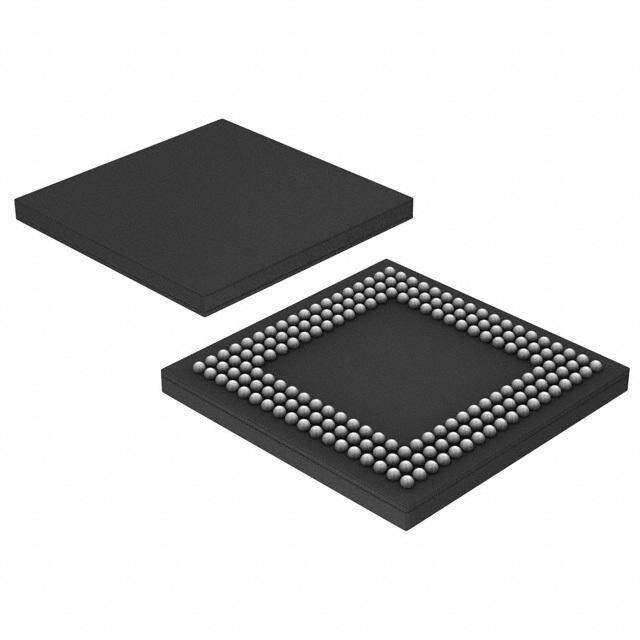
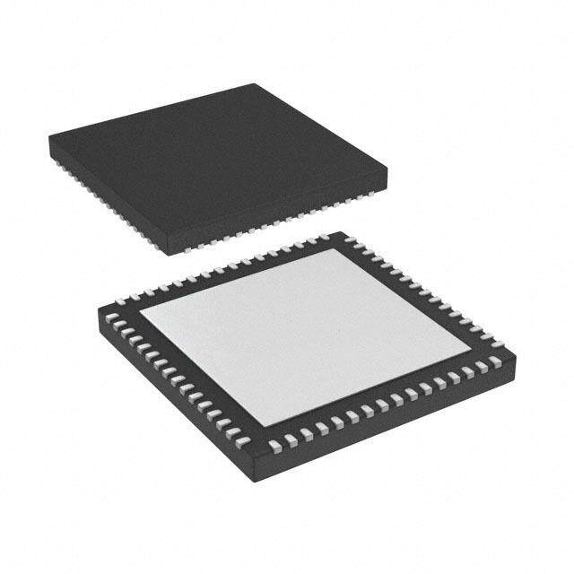
| 供应商器件封装 | 40-WQFN(5x5) |
| 其它名称 | 296-29345-6 |
| 制造商产品页 | http://www.ti.com/general/docs/suppproductinfo.tsp?distId=10&orderablePartNumber=MSP430F5132IRSBR |
| 包装 | Digi-Reel® |
| 外设 | 欠压检测/复位,DMA,POR,PWM,WDT |
| 封装/外壳 | 40-WFQFN 裸露焊盘 |
| 工作温度 | -40°C ~ 85°C |
| 振荡器类型 | 内部 |
| 数据转换器 | A/D 11x10b |
| 标准包装 | 1 |
| 核心处理器 | MSP430 |
| 核心尺寸 | 16-位 |
| 电压-电源(Vcc/Vdd) | 1.8 V ~ 3.6 V |
| 程序存储器类型 | 闪存 |
| 程序存储容量 | 8KB(8K x 8) |
| 连接性 | I²C, IrDA, SCI, SPI, UART/USART |
| 速度 | 25MHz |


- 商务部:美国ITC正式对集成电路等产品启动337调查
- 曝三星4nm工艺存在良率问题 高通将骁龙8 Gen1或转产台积电
- 太阳诱电将投资9.5亿元在常州建新厂生产MLCC 预计2023年完工
- 英特尔发布欧洲新工厂建设计划 深化IDM 2.0 战略
- 台积电先进制程称霸业界 有大客户加持明年业绩稳了
- 达到5530亿美元!SIA预计今年全球半导体销售额将创下新高
- 英特尔拟将自动驾驶子公司Mobileye上市 估值或超500亿美元
- 三星加码芯片和SET,合并消费电子和移动部门,撤换高东真等 CEO
- 三星电子宣布重大人事变动 还合并消费电子和移动部门
- 海关总署:前11个月进口集成电路产品价值2.52万亿元 增长14.8%


PDF Datasheet 数据手册内容提取
Product Order Technical Tools & Support & Folder Now Documents Software Community MSP430F5172,MSP430F5152,MSP430F5132 MSP430F5171,MSP430F5151,MSP430F5131 SLAS619R–AUGUST2010–REVISEDSEPTEMBER2018 MSP430F51x2, MSP430F51x1 Mixed-Signal Microcontrollers 1 Device Overview 1.1 Features 1 • LowSupply-VoltageRange: • 16-BitTimerTD1WithThreeCapture/Compare 3.6VDownto1.8V RegistersandSupportofHigh-ResolutionMode • Ultra-LowPowerConsumption • 16-BitTimerTA0WithThreeCapture/Compare – ActiveMode(AM):180 µA/MHz Registers – StandbyMode(LPM3WDTMode,3V):1.1 µA • UniversalSerialCommunicationInterfaces (USCIs) (1) – OffMode(LPM4RAMRetention,3V):0.9 µA – USCI_A0Supports: – ShutdownMode(LPM4.5,3V):0.25 µA – EnhancedUARTSupportsAutomaticBaud- • WakeupFromStandbyModeinLessThan5µs RateDetection • 16-BitRISCArchitecture,ExtendedMemory,40-ns – IrDAEncoderandDecoder InstructionCycleTime – SynchronousSPI • FlexiblePower-ManagementSystem – USCI_B0Supports: – FullyIntegratedLDOWithProgrammable RegulatedCoreSupplyVoltage – I2C – SupplyVoltageSupervision,Monitoring,and – SynchronousSPI Brownout • 10-Bit200-kspsAnalog-to-DigitalConverter(ADC) • UnifiedClockSystem – InternalReference – FLLControlLoopforFrequencyStabilization – Sample-and-Hold – Low-PowerLow-FrequencyInternalClock – AutoscanFeature Source(VLO) – Upto8ExternalChannelsand2Internal – Low-FrequencyTrimmedInternalReference Channels,IncludingTemperatureSensor(1) Source(REFO) • Upto16-ChannelOn-ChipComparatorIncluding – 32-kHzCrystals(XT1) anUltra-Low-PowerMode(1) – High-FrequencyCrystalsupto25MHz(XT1) • SerialOnboardProgramming,NoExternal • HardwareMultiplierSupports32-BitOperations ProgrammingVoltageNeeded • 3-ChannelDMA • DeviceComparisonSummarizestheAvailable FamilyMembers • UptoTwelve5-V-TolerantDigitalPush/PullI/Os Withupto20-mADriveStrength(1) • Availablein40-PinQFN(RSB),38-PinTSSOP (DA),and40-PinDie-SizedBGA(YFF)Packages • 16-BitTimerTD0WithThreeCapture/Compare RegistersandSupportofHigh-ResolutionMode (1) Fullfunctionalityinthe40-pinQFNpackageoptions.Forthe availablefeaturesofotherpackages,seeSignalDescriptions. 1.2 Applications • AnalogandDigitalSensorSystems • MotorControls • LEDLighting • RemoteControls • DigitalPowerSupplies • Thermostats 1 An IMPORTANT NOTICE at the end of this data sheet addresses availability, warranty, changes, use in safety-critical applications, intellectualpropertymattersandotherimportantdisclaimers.PRODUCTIONDATA.
MSP430F5172,MSP430F5152,MSP430F5132 MSP430F5171,MSP430F5151,MSP430F5131 SLAS619R–AUGUST2010–REVISEDSEPTEMBER2018 www.ti.com 1.3 Description The TI MSP family of ultra-low-power microcontrollers consists of several devices featuring different sets of peripherals targeted for various applications. The architecture, combined with five low-power modes, is optimized to achieve extended battery life in portable measurement applications. The device features a powerful 16-bit RISC CPU, 16-bit registers, and constant generators that contribute to maximum code efficiency.Thedigitallycontrolledoscillator(DCO)allowsthedevicestowakeupfromlow-powermodesto activemodeinlessthan5 µs. The MSP430F51x2 microcontrollers include two 16-bit high-resolution timers, two USCIs (USCI_A0 and USCI_B0), a 32-bit hardware multiplier, a high-performance 10-bit ADC, an on-chip comparator, a 3- channelDMA,5-VtolerantI/Os,andupto29I/Opins. The MSP430F51x1 microcontrollers include two 16-bit high-resolution timers, two USCIs (USCI_A0 and USCI_B0), a 32-bit hardware multiplier, an on-chip comparator, a 3-channel DMA, 5-V tolerant I/Os, and upto29I/Opins. Typical applications for these devices include analog and digital sensor systems, LED lighting, digital powersupplies,motorcontrols,remotecontrols,thermostats,digitaltimers,andhand-heldmeters. Forcompletemoduledescriptions,seethe MSP430F5xxandMSP430F6xxFamilyUser'sGuide. DeviceInformation(1) PARTNUMBER PACKAGE BODYSIZE(2) MSP430F5172IYFF DSBGA(40) SeeSection8 MSP430F5172IRSB WQFN(40) 5mm×5mm MSP430F5172IDA TSSOP(38) 12.5mm×6.2mm (1) Forthemostcurrentpart,package,andorderinginformation,seethePackageOptionAddendumin Section8,orseetheTIwebsiteatwww.ti.com. (2) Thedimensionsshownhereareapproximations.Forthepackagedimensionswithtolerances,seethe MechanicalDatainSection8. 2 DeviceOverview Copyright©2010–2018,TexasInstrumentsIncorporated SubmitDocumentationFeedback ProductFolderLinks:MSP430F5172 MSP430F5152 MSP430F5132MSP430F5171 MSP430F5151 MSP430F5131
MSP430F5172,MSP430F5152,MSP430F5132 MSP430F5171,MSP430F5151,MSP430F5131 www.ti.com SLAS619R–AUGUST2010–REVISEDSEPTEMBER2018 1.4 Functional Block Diagrams Figure1-1showsthefunctionalblockdiagramfortheMSP430F51x2devices. DVCC AVCC DVIO P1.x P2.x P3.x PJ.x XINXOUT RST/NMI DVSS AVSS DVSS 8 8 8 7 I/O Ports I/O Ports I/O Ports I/O Ports ACLK Unified Power SYS Clock 32KB 2KB Management P1 P2 P3 PJ System SMCLK 16KB 2KB Watchdog 2x 58 V I,/ O20s mA 8x58 V I,/ O20s mA 2x58 V I,/ O20s mA 7 I/Os 8KB 1KB Interrupt Interrupt LDO Port and Wakeup, and Wakeup, Flash RAM SVM, SVS Mapping Pullup or Pullup or Pullup or Pullup or Brownout Controller MCLK Pulldown Pulldown Pulldown Pulldown Resistors Resistors Resistors Resistors CPUXV2 3 DMA and Working Channel Registers EEM (S: 3+1) TD0 TD1 COMP_B JSTBAWG, TA0 Timer_D Timer_D USCI ADC10_A 16 Channels REF Interface MPY32 Ti3m CerC_A ≤R2e53g6 Ci sMCteHrsz ≤R2e53g6 Ci sMCteHrsz AIr0D: AU,A SRPTI, 20100 K BSiPtS MedHiuigmh--,, and Voltage CRC16 Registers With Buffer With Buffer B0: SPI, I2C 9 Channels Ultra-Low- Reference Event Event Power Control Control Modes Copyright © 2017,Texas Instruments Incorporated Figure1-1.FunctionalBlockDiagram,MSP430F51x2 Figure1-2showsthefunctionalblockdiagramfortheMSP430F51x1devices. DVCC AVCC DVIO P1.x P2.x P3.x PJ.x XINXOUT RST/NMI DVSS AVSS DVSS 8 8 8 7 I/O Ports I/O Ports ACLK I/O Ports I/O Ports Unified Power SYS Clock P1 P2 32KB 2KB Management P3 PJ System 8 I/Os 8 I/Os SMCLK 16KB 2KB Watchdog 2x 5 V, 20 mA 8x 5 V, 20 mA 8 I/Os 7 I/Os 8KB 1KB 2x 5 V, 20 mA Interrupt Interrupt LDO Port and Wakeup, and Wakeup, Flash RAM SVM, SVS Mapping Pullup or Pullup or Pullup or Pullup or Brownout Controller Pulldown Pulldown MCLK Pulldown Pulldown Resistors Resistors Resistors Resistors CPUXV2 3 DMA and Working Channel Registers EEM (S: 3+1) TD0 TD1 COMP_B JSTBAWG, TA0 Timer_D Timer_D USCI 16 Channels REF Interface MPY32 Ti3m CerC_A ≤R2e53g6 Ci sMCteHrsz ≤R2e53g6 Ci sMCteHrsz AIr0D: AU,A SRPTI, MedHiuigmh--,, and Voltage CRC16 Registers With Buffer With Buffer B0: SPI, I2C Ultra-Low- Reference Event Event Power Control Control Modes Copyright © 2017,Texas Instruments Incorporated Figure1-2.FunctionalBlockDiagram,MSP430F51x1 Copyright©2010–2018,TexasInstrumentsIncorporated DeviceOverview 3 SubmitDocumentationFeedback ProductFolderLinks:MSP430F5172 MSP430F5152 MSP430F5132MSP430F5171 MSP430F5151 MSP430F5131
MSP430F5172,MSP430F5152,MSP430F5132 MSP430F5171,MSP430F5151,MSP430F5131 SLAS619R–AUGUST2010–REVISEDSEPTEMBER2018 www.ti.com Table of Contents 1 DeviceOverview......................................... 1 5.26 PMM,BrownoutReset(BOR)....................... 31 .............................................. ................................. 1.1 Features 1 5.27 PMM,CoreVoltage 31 ........................................... ............................... 1.2 Applications 1 5.28 PMM,SVSHighSide 32 ............................................ ............................... 1.3 Description 2 5.29 PMM,SVMHighSide 33 ........................... ................................ 1.4 FunctionalBlockDiagrams 3 5.30 PMM,SVSLowSide 33 2 Revision History......................................... 5 5.31 PMM,SVMLowSide............................... 33 3 DeviceComparison ..................................... 6 5.32 Wake-upTimesFromLow-PowerModes.......... 34 ..................................... ............................................. 3.1 RelatedProducts 7 5.33 Timer_A 34 4 TerminalConfigurationandFunctions.............. 8 5.34 USCI(UARTMode)................................. 34 ......................................... ............................ 4.1 PinDiagrams 8 5.35 USCI(SPIMasterMode) 35 .................................. ............................. 4.2 SignalDescriptions 11 5.36 USCI(SPISlaveMode) 37 5 Specifications........................................... 14 5.37 USCI(I2CMode).................................... 39 5.1 AbsoluteMaximumRatings ........................ 14 5.38 10-BitADC,PowerSupplyandInputRange .......... ........................................ Conditions(MSP430F51x2DevicesOnly) 40 5.2 ESDRatings 14 ............... 5.39 10-BitADC,TimingParameters(MSP430F51x2 5.3 RecommendedOperatingConditions 14 ....................................... Devices Only) 40 5.4 ActiveModeSupplyCurrentIntoV Excluding ....................C.C................ 5.40 10-BitADC,LinearityParameters(MSP430F51x2 External Current 16 ....................................... Devices Only) 41 5.5 Low-PowerModeSupplyCurrents(IntoV ) ................C.C......... 5.41 REF,ExternalReference(MSP430F51x2Devices ExcludingExternalCurrent 16 ................................................. Only) 41 ................ 5.6 ThermalResistanceCharacteristics 17 5.42 REF,Built-InReference(MSP430F51x2Devices 5.7 Schmitt-TriggerInputs–General-PurposeI/O(P1.0 ................................................. Only) 42 ............ toP1.5,P3.2toP3.7,andPJ.0toPJ.6) 17 ....................................... 5.43 Comparator_B 43 5.8 Schmitt-TriggerInputs–General-PurposeI/O(P1.6 ...... ........ 5.44 Timer_D,PowerSupplyandReferenceClock 44 andP1.7,P2.0toP2.7,andP3.0andP3.1) 17 ........ ........................... 5.45 Timer_D,LocalClockGeneratorFrequency 45 5.9 Inputs–PortsP1andP2 17 .............. ........... 5.46 Timer_D,TrimmedClockFrequencies 47 5.10 LeakageCurrent–General-PurposeI/O 18 ........... 5.11 Outputs–PortsP1,P3,PJ(FullDriveStrength, 5.47 Timer_D,FrequencyMultiplicationMode 47 P1.0toP1.5,P3.2toP3.7,PJ.0toPJ.6)........... 18 5.48 Timer_D,InputCaptureandOutputCompare ............................................... 5.12 Outputs–PortsP1toP3(FullDriveStrength,P1.6 Timing 48 ............ ....................................... andP1.7,P2.0toP2.7,P3.0andP3.1) 18 5.49 FlashMemory 49 5.13 Outputs–PortsP1,P3,PJ(ReducedDrive 5.50 JTAGandSpy-Bi-WireInterface.................... 49 . Strength,P1.0toP1.5,P3.2toP3.7,PJ.0toPJ.6) 19 6 DetailedDescription................................... 50 5.14 Outputs–PortsP1toP3(ReducedDriveStrength, ................................................. ....... 6.1 CPU 50 P1.6andP1.7,P2.0toP2.7,P3.0andP3.1) 19 ....................................... 6.2 InstructionSet 51 5.15 OutputFrequency–PortsP1.0toP1.5,P3.2to P3.7,PJ.0toPJ.6................................... 20 6.3 OperatingModes.................................... 52 .......................... 5.16 OutputFrequency–PortsP1.6andP1.7,P2.0to 6.4 InterruptVectorAddresses 53 P2.7,P3.0andP3.1................................. 20 6.5 Memory Organization............................... 54 5.17 TypicalCharacteristics–Outputs,ReducedDrive 6.6 Bootloader(BSL).................................... 54 Strength(PxDS.y=0),PortsP1.0toP1.5,P3.2to ....................................... ................................... 6.7 FlashMemory 55 P3.7,PJ.0toPJ.6 21 ................................................. 6.8 RAM 55 5.18 TypicalCharacteristics–Outputs,FullDrive .......................................... Strength(PxDS.y=1),PortsP1.0toP1.5,P3.2to 6.9 Peripherals 55 P3.7,PJ.0toPJ.6................................... 22 6.10 Input/OutputDiagrams.............................. 74 5.19 TypicalCharacteristics–Outputs,ReducedDrive .................................. 6.11 Device Descriptors 91 Strength(PxDS.y=0),PortsP1.6andP1.7,P2.0to ................................. 7 DeviceandDocumentationSupport............... 97 P2.7,P3.0andP3.1 23 ..................... 5.20 TypicalCharacteristics–Outputs,FullDrive 7.1 GettingStartedandNextSteps 97 Strength(PxDS.y=1),PortsP1.6andP1.7,P2.0to 7.2 Device Nomenclature............................... 97 ................................. P2.7,P3.0andP3.1 25 ................................. 7.3 ToolsandSoftware 99 ..... 5.21 CrystalOscillator,XT1,Low-FrequencyMode 27 ............................ 7.4 DocumentationSupport 101 .... 5.22 CrystalOscillator,XT1,High-FrequencyMode 28 ...................................... 7.5 RelatedLinks 102 5.23 InternalVery-Low-PowerLow-FrequencyOscillator ............................. ................................................ 7.6 CommunityResources 102 (VLO) 29 ........................................ 7.7 Trademarks 102 5.24 InternalReference,Low-FrequencyOscillator (REFO).............................................. 29 7.8 ElectrostaticDischargeCaution................... 103 5.25 DCO Frequency..................................... 30 7.9 ExportControlNotice.............................. 103 4 TableofContents Copyright©2010–2018,TexasInstrumentsIncorporated SubmitDocumentationFeedback ProductFolderLinks:MSP430F5172 MSP430F5152 MSP430F5132MSP430F5171 MSP430F5151 MSP430F5131
MSP430F5172,MSP430F5152,MSP430F5132 MSP430F5171,MSP430F5151,MSP430F5131 www.ti.com SLAS619R–AUGUST2010–REVISEDSEPTEMBER2018 7.10 Glossary............................................ 103 8 Mechanical,Packaging,andOrderable Information............................................. 104 2 Revision History ChangesfromJuly20,2018toSeptember20,2018 Page • AddedtypicalconditionsstatementsatthebeginningofSection5,Specifications........................................ 14 • UpdatedSection7.4,DocumentationSupport................................................................................. 101 Copyright©2010–2018,TexasInstrumentsIncorporated RevisionHistory 5 SubmitDocumentationFeedback ProductFolderLinks:MSP430F5172 MSP430F5152 MSP430F5132MSP430F5171 MSP430F5151 MSP430F5131
MSP430F5172,MSP430F5152,MSP430F5132 MSP430F5171,MSP430F5151,MSP430F5131 SLAS619R–AUGUST2010–REVISEDSEPTEMBER2018 www.ti.com 3 Device Comparison Table3-1summarizestheavailablefamilymembers. Table3-1.DeviceComparison(1)(2) USCI DEVICE F(LKABS)H S(RKABM) Timer_A(3) Timer_D(4) CUHAARNTN,IErDLAA,: CHANNELB: AD(CC1h0)_A Co(mChp)_B I/Os PACKAGE SPI,I2C SPI 40QFN 9ext,2int 16 31 MSP430F5172 32 2 3 3,3 1 1 40DSBGA 8ext,2int 15 29 38TSSOP 40QFN 9ext,2int 16 31 MSP430F5152 16 2 3 3,3 1 1 40DSBGA 8ext,2int 15 29 38TSSOP 40QFN 9ext,2int 16 31 MSP430F5132 8 1 3 3,3 1 1 40DSBGA 8ext,2int 15 29 38TSSOP 40QFN 16 31 MSP430F5171 32 2 3 3,3 1 1 – 40DSBGA 15 29 38TSSOP 40QFN 16 31 MSP430F5151 16 2 3 3,3 1 1 – 40DSBGA 15 29 38TSSOP 40QFN 16 31 MSP430F5131 8 1 3 3,3 1 1 – 40DSBGA 15 29 38TSSOP (1) Forthemostcurrentpackageandorderinginformation,seethePackageOptionAddenduminSection8,orseetheTIwebsiteat www.ti.com. (2) Packagedrawings,thermaldata,andsymbolizationareavailableatwww.ti.com/packaging. (3) EachnumberinthesequencerepresentsaninstantiationofTimer_AwithitsassociatednumberofcapturecompareregistersandPWM outputgeneratorsavailable.Forexample,anumbersequenceof3,5wouldrepresenttwoinstantiationsofTimer_A,thefirst instantiationhaving3andthesecondinstantiationhaving5capturecompareregistersandPWMoutputgenerators,respectively. (4) EachnumberinthesequencerepresentsaninstantiationofTimer_DwithitsassociatednumberofcapturecompareregistersandPWM outputgeneratorsavailable.Forexample,anumbersequenceof3,5wouldrepresenttwoinstantiationsofTimer_D,thefirst instantiationhaving3andthesecondinstantiationhaving5capturecompareregistersandPWMoutputgenerators,respectively. 6 DeviceComparison Copyright©2010–2018,TexasInstrumentsIncorporated SubmitDocumentationFeedback ProductFolderLinks:MSP430F5172 MSP430F5152 MSP430F5132MSP430F5171 MSP430F5151 MSP430F5131
MSP430F5172,MSP430F5152,MSP430F5132 MSP430F5171,MSP430F5151,MSP430F5131 www.ti.com SLAS619R–AUGUST2010–REVISEDSEPTEMBER2018 3.1 Related Products Forinformationaboutotherdevicesinthisfamilyofproductsorrelatedproducts,seethefollowinglinks. TI16-bitand32-bitmicrocontrollers High-performance, low-power solutions to enable the autonomous future ProductsforMSP430ultra-low-powersensingandmeasurementmicrocontrollers One platform. Oneecosystem.Endlesspossibilities. ProductsforMSP430ultra-low-powermicrocontrollers MCUs for metrology, monitoring, system control,andcommunications CompanionProductsforMSP430F5172 Review products that are frequently purchased or used in conjunctionwiththisproduct. ReferenceDesignsforMSP430F5172 TI Designs Reference Design Library is a robust reference design library that spans analog, embedded processor, and connectivity. Created by TI experts to help you jump start your system design, all TI Designs include schematic or block diagrams, BOMs, and design files to speed your time to market. Search and download designs at ti.com/tidesigns. Copyright©2010–2018,TexasInstrumentsIncorporated DeviceComparison 7 SubmitDocumentationFeedback ProductFolderLinks:MSP430F5172 MSP430F5152 MSP430F5132MSP430F5171 MSP430F5151 MSP430F5131
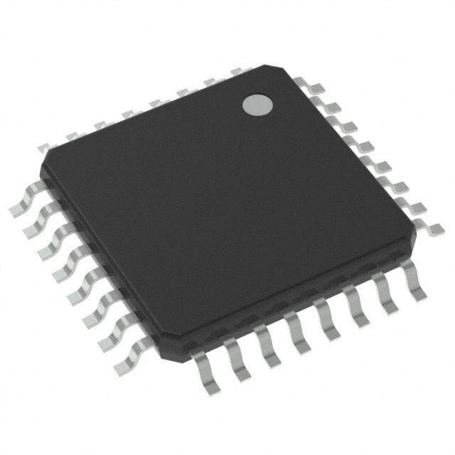
MSP430F5172,MSP430F5152,MSP430F5132 MSP430F5171,MSP430F5151,MSP430F5131 SLAS619R–AUGUST2010–REVISEDSEPTEMBER2018 www.ti.com 4 Terminal Configuration and Functions 4.1 Pin Diagrams Figure4-1showsthepinoutforthe40-pinRSBpackage. B11B12 CC 10REF/-*RE/F+* MCLK BEE _ CVV M 0.0/A6*/0.1/A7*/0.2/A8*/WTDIOCK 0CLK/P AAABT D T TTTSW T SS 5/XIN 4/XOUCC7/PM_6/PM_5/PM_T/NMI/ST/SB 4/PM_ V J. J.V3.3.3.SE 3. A P PAPPPRT P P1.0/PM_UCA0CLK/PM_UCB0STE/A0*/CB0 1 3938373635343332 P3.3/PM_TA0CLK/PM_CBOUT/CB13 P1.1/PM_UCA0TXD/PM_UCA0SIMO/A1*/CB1 2 29 P3.2/PM_TD0.0/PM_SMCLK/CB14 P1.2/PM_UCA0RXD/PM_UCA0SOMI/A2*/CB2 3 28 PJ.6/TD1CLK/TD0.1/CB15 P1.3/PM_UCB0CLK/PM_UCA0STE/A3*/CB3 4 27 DVCC P1.4/PM_UCB0SIMO/PM_UCB0SDA/A4*/CB4 5 26 DVSS P1.5/PM_UCB0SOMI/PM_UCB0SCL/A5*/CB5 6 25 VCORE PJ.0/SMCLK/TDO/CB6 7 24 P3.1/PM_TEC1FLT0/PM_TD1.2 PJ.1/MCLK/TDI/TCLK/CB7 8 23 P3.0/PM_TEC1FLT2/PM_TD1.1 PJ.2/ADC10CLK/TMS/CB8 9 22 P2.7/PM_TEC1CLR/PM_TEC1FLT1/PM_TD1.0 PJ.3/ACLK/TCK/CB9 1213141516171819 P2.6/PM_TEC0FLT1/PM_TD0.2 P1.6/TD0PM_.0P1.7/TDPM_0.1P2.0/PM_TD0.2P2.1/P M_TD1.0 P2.2/TPM_D1.1 P2.3/TPM_D1.2DVIODVSS FLT2 /TPM_D0.0 FLT0/PM_TD0.1 0 0 C C E E T T _ _ M M P P /R 5/ L 2. C P 0 C E T _ M P 4/ * Only MSP430F51x2 devices 2. P Figure4-1.40-PinRSBPackage(TopView) 8 TerminalConfigurationandFunctions Copyright©2010–2018,TexasInstrumentsIncorporated SubmitDocumentationFeedback ProductFolderLinks:MSP430F5172 MSP430F5152 MSP430F5132MSP430F5171 MSP430F5151 MSP430F5131
MSP430F5172,MSP430F5152,MSP430F5132 MSP430F5171,MSP430F5151,MSP430F5131 www.ti.com SLAS619R–AUGUST2010–REVISEDSEPTEMBER2018 Figure4-2showsthepinoutforthe38-pinDApackage. AVCC 1 38 P3.6/PM_TA0.1/A7*/VEREF-*/CB11 - PJ.4/XOUT 2 37 P3.5/PM_TA0.2/A8*/VEREF+*/CB12 PJ.5/XIN 3 36 RST/NMI/SBWTDIO AVSS 4 35 TEST/SBWTCK P1.0/PM_UCA0CLK/PM_UCB0STE/A0*/CB0 5 34 P3.3/PM_TA0CLK/PM_CBOUT/CB13 P1.1/PM_UCA0TXD/PM_UCA0SIMO/A1*/CB1 6 33 P3.2/PM_TD0.0/PM_SMCLK/CB14 P1.2/PM_UCA0RXD/PM_UCA0SOMI/A2*/CB2 7 32 PJ.6/TD1CLK/TD0.1/CB15 P1.3/PM_UCB0CLK/PM_UCA0STE/A3*/CB3 8 31 DVCC P1.4/PM_UCB0SIMO/PM_UCB0SDA/A4*/CB4 9 30 DVSS P1.5/PM_UCB0SOMI/PM_UCB0SCL/A5*/CB5 10 29 VCORE PJ.0/SMCLK/TDO/CB6 11 28 P3.1/PM_TEC1FLT0/PM_TD1.2 PJ.1/MCLK/TDI/TCLK/CB7 12 27 P3.0/PM_TEC1FLT2/PM_TD1.1 PJ.2/ADC10CLK/TMS/CB8 13 26 P2.7/PM_TEC1CLR/PM_TEC1FLT1/PM_TD1.0 PJ.3/ACLK/TCK/CB9 14 25 P2.6/PM_TEC0FLT1/PM_TD0.2 P1.6/PM_TD0.0 15 24 P2.5/PM_TEC0FLT0/PM_TD0.1 P1.7/PM_TD0.1 16 23 P2.4/PM_TEC0CLR/PM_TEC0FLT2 /PM_TD0.0 P2.0/PM_TD0.2 17 22 DVSS P2.1/PM _ TD1.0 18 21 DVIO * Only MSP430F51x2 P2.2/PM_TD1.1 19 20 P2.3/PM_TD1.2 Figure4-2.38-PinDAPackage(TopView) Copyright©2010–2018,TexasInstrumentsIncorporated TerminalConfigurationandFunctions 9 SubmitDocumentationFeedback ProductFolderLinks:MSP430F5172 MSP430F5152 MSP430F5132MSP430F5171 MSP430F5151 MSP430F5131
MSP430F5172,MSP430F5152,MSP430F5132 MSP430F5171,MSP430F5151,MSP430F5131 SLAS619R–AUGUST2010–REVISEDSEPTEMBER2018 www.ti.com Figure4-3showsthepinoutforthe40-pinYFFpackage.Forthepackagedimensions,seethe Mechanical DatainSection8. Top View Ball-Side View P1.6 P2.1 P2.2 DVIO DVSS P2.5 P2.5 DVSS DVIO P2.2 P2.1 P1.6 G6 G5 G4 G3 G2 G1 G1 G2 G3 G4 G5 G6 PJ.2 P1.7 P2.0 P2.4 P2.6 P3.0 P3.0 P2.6 P2.4 P2.0 P1.7 PJ.2 F6 F5 F4 F3 F2 F1 F1 F2 F3 F4 F5 F6 PJ.0 PJ.1 PJ.3 P2.3 P2.7 P3.1 P3.1 P2.7P2.3 PJ.3 PJ.1 PJ.0 E6 E5 E4 E3 E2 E1 E1 E2 E3 E4 E5 E6 P1.5 P1.4 TEST VCORE VCORE TEST P1.4 P1.5 D6 D5 D2 D1 D1 D2 D5 D6 P1.3 P1.2 AVSS AVCC PJ.6 DVSS DVSS PJ.6 AVCC AVSS P1.2 P1.3 C6 C5 C4 C3 C2 C1 C1 C2 C3 C4 C5 C6 P1.1 P1.0 P3.7 RST P3.2 DVCC DVCC P3.2 RST P3.7 P1.0 P1.1 B6 B5 B4 B3 B2 B1 B1 B2 B3 B4 B5 B6 XIN XOUT P3.6 P3.5 P3.4 P3.3 P3.3 P3.4 P3.5 P3.6 XOUT XIN A6 A5 A4 A3 A2 A1 A1 A2 A3 A4 A5 A6 Figure4-3.40-PinYFFPackage(TopViewandBottomView) 10 TerminalConfigurationandFunctions Copyright©2010–2018,TexasInstrumentsIncorporated SubmitDocumentationFeedback ProductFolderLinks:MSP430F5172 MSP430F5152 MSP430F5132MSP430F5171 MSP430F5151 MSP430F5131
MSP430F5172,MSP430F5152,MSP430F5132 MSP430F5171,MSP430F5151,MSP430F5131 www.ti.com SLAS619R–AUGUST2010–REVISEDSEPTEMBER2018 4.2 Signal Descriptions Table4-1describesthesignalsforalldeviceandpackagevariants. Table4-1.SignalDescriptions TERMINAL NO.(2) I/O(1) DESCRIPTION NAME RSB DA YFF P1.0/ General-purposedigitalI/Owithreconfigurableportmappingsecondaryfunction(4) PM_UCA0CLK/ Defaultmapping:Clocksignalinput–USCI_A0SPIslavemode;Clocksignaloutput– <br/> USCI_A0SPImastermode 1 5 B5 I/O PM_UCB0STE/ Defaultmapping:Slavetransmitenable–USCI_B0SPImode A0(3)/ AnaloginputA0–10-bitADC(3) CB0 Comparator_BInput0 P1.1/ General-purposedigitalI/O PM_UCA0TXD/ Defaultmapping:Transmitdata–USCI_A0UARTmode PM_UCA0SIMO/ 2 6 B6 I/O Defaultmapping:Slavein,masterout–USCI_A0SPImode A1(3)/ AnaloginputA1–10-bitADC(3) CB1 Comparator_BInput1 P1.2/ General-purposedigitalI/Owithreconfigurableportmappingsecondaryfunction PM_UCA0RXD/ Defaultmapping:Receivedata–USCI_A0UARTmode PM_UCA0SOMI/ 3 7 C5 I/O Defaultmapping:Slaveout,masterin–USCI_A0SPImode A2(3)/ AnaloginputA2–10-bitADC(3) CB2 Comparator_BInput2 P1.3/ General-purposedigitalI/Owithreconfigurableportmappingsecondaryfunction PM_UCB0CLK/ Defaultmapping:Clocksignalinput–USCI_B0SPIslavemode;Clocksignaloutput– <br/> USCI_B0SPImastermode 4 8 C6 I/O PM_UCA0STE/ Defaultmapping:Slavetransmitenable–USCI_A0SPImode A3(3)/ AnaloginputA3–10-bitADC(3) CB3 Comparator_BInput3 P1.4/ General-purposedigitalI/Owithreconfigurableportmappingsecondaryfunction PM_UCB0SIMO/ Defaultmapping:Slavein,masterout–USCI_B0SPImode PM_UCB0SDA/ 5 9 D5 I/O Defaultmapping:I2Cdata–USCI_B0I2Cmode A4(3)/ AnaloginputA4–10-bitADC(3) CB4 Comparator_BInput4 P1.5/ General-purposedigitalI/Owithreconfigurableportmappingsecondaryfunction PM_UCB0SOMI/ Defaultmapping:Slaveout,masterin–USCI_B0SPImode PM_UCB0SCL/ 6 10 D6 I/O Defaultmapping:I2Cclock–USCI_B0I2Cmode A5(3)/ AnaloginputA5–10-bitADC(3) CB5 Comparator_BInput5 PJ.0/ General-purposedigitalI/O SMCLK/ SMCLKclockoutput 7 11 E6 I/O TDO/ Testdataoutputport CB6 Comparator_BInput6 PJ.1/ General-purposedigitalI/O MCLK/ MCLKclockoutput 8 12 E5 I/O TDI/TCLK/ Testdatainputortestclockinput CB7 Comparator_BInput7 PJ.2/ General-purposedigitalI/O ADC10CLK/ ADC10_Aclockoutput 9 13 F6 I/O TMS/ Testmodeselect CB8 Comparator_BInput8 PJ.3/ General-purposedigitalI/O ACLK/ ACLKoutputport 10 14 E4 I/O TCK/ Testclock CB9 Comparator_BInput9 P1.6/ I/O, General-purposedigitalI/Owithreconfigurableportmappingsecondaryfunction 11 15 G6 PM_TD0.0 DV Defaultmapping:TD0CCR0compareoutput/captureinput IO (1) I=input,O=output (2) N/A=notavailableonthispackageoffering (3) TheADC10_AmoduleisavailableonMSP430F51x2devices.ThesecondarypinfunctionsAx(ADC10_Achannelx)availableonlyin MSP430F51x2devices. (4) FordetailsonthePortMappingController,seeSection6.9.2. Copyright©2010–2018,TexasInstrumentsIncorporated TerminalConfigurationandFunctions 11 SubmitDocumentationFeedback ProductFolderLinks:MSP430F5172 MSP430F5152 MSP430F5132MSP430F5171 MSP430F5151 MSP430F5131
MSP430F5172,MSP430F5152,MSP430F5132 MSP430F5171,MSP430F5151,MSP430F5131 SLAS619R–AUGUST2010–REVISEDSEPTEMBER2018 www.ti.com Table4-1.SignalDescriptions(continued) TERMINAL NO.(2) I/O(1) DESCRIPTION NAME RSB DA YFF P1.7/ I/O, General-purposedigitalI/Owithreconfigurableportmappingsecondaryfunction 12 16 F5 PM_TD0.1 DV Defaultmapping:TD0CCR1compareoutput/captureinput IO P2.0/ I/O, General-purposedigitalI/Owithreconfigurableportmappingsecondaryfunction 13 17 F4 PM_TD0.2 DV Defaultmapping:TD0CCR2compareoutput/captureinput IO P2.1/ I/O, General-purposedigitalI/Owithreconfigurableportmappingsecondaryfunction 14 18 G5 PM_TD1.0 DV Defaultmapping:TD1CCR0compareoutput/captureinput IO P2.2/ I/O, General-purposedigitalI/Owithreconfigurableportmappingsecondaryfunction 15 19 G4 PM_TD1.1 DV Defaultmapping:TD1CCR1compareoutput/captureinput IO P2.3/ I/O, General-purposedigitalI/Owithreconfigurableportmappingsecondaryfunction 16 20 E3 PM_TD1.2 DV Defaultmapping:TD1CCR2compareoutput/captureinput IO DVIO 17 21 G3 5-VtolerantdigitalI/Opowersupply DVSS 18 22 G2 Digitalgroundsupply P2.4/ General-purposedigitalI/Owithreconfigurableportmappingsecondaryfunction PM_TEC0CLR/ I/O, Defaultmapping:TD0externalclearinput 19 23 F3 PM_TEC0FLT2/ DV Defaultmapping:TD0faultinputchannel2(controlledbymoduleinputenable) IO PM_TD0.0 Defaultmapping:TD0CCR0compareoutput P2.5/ General-purposedigitalI/Owithreconfigurableportmappingsecondaryfunction I/O, PM_TEC0FLT0/ 20 24 G1 Defaultmapping:TD0faultinputchannel0 DV PM_TD0.1 IO Defaultmapping:TD0CCR1compareoutput P2.6/ General-purposedigitalI/Owithreconfigurableportmappingsecondaryfunction I/O, PM_TEC0FLT1/ 21 25 F2 Defaultmapping:TD0faultinputchannel1 DV PM_TD0.2 IO Defaultmapping:TD0CCR2compareoutput P2.7/ General-purposedigitalI/Owithreconfigurableportmappingsecondaryfunction PM_TEC1CLR/ I/O, Defaultmapping:TD1externalclear 22 26 E2 PM_TEC1FLT1/ DV Defaultmapping:TD1faultinputchannel1(controlledbymoduleinputenable) IO PM_TD1.0 Defaultmapping:TD1CCR0compareoutput P3.0/ General-purposedigitalI/Owithreconfigurableportmappingsecondaryfunction I/O, PM_TEC1FLT2/ 23 27 F1 Defaultmapping:TD1faultinputchannel2 DV PM_TD1.1 IO Defaultmapping:TD1CCR1compareoutput P3.1/ General-purposedigitalI/Owithreconfigurableportmappingsecondaryfunction I/O, PM_TEC1FLT0/ 24 28 E1 Defaultmapping:TD1faultinputchannel0 DV PM_TD1.2 IO Defaultmapping:TD1CCR2compareoutput VCORE 25 29 D1 Regulatedcorepowersupply DVSS 26 30 C1 Digitalgroundsupply DVCC 27 31 B1 Digitalpowersupply PJ.6/ General-purposedigitalI/O TD1CLK/ TD1clockinput 28 32 C2 I/O TD0.1/ TD0CCR1compareoutput CB15 Comparator_BInput15 P3.2/ General-purposedigitalI/Owithreconfigurableportmappingsecondaryfunction PM_TD0.0/ Defaultmapping:TD0CCR0captureinput 29 33 B2 I/O PM_SMCLK/ Defaultmapping:SMCLKoutput CB14 Comparator_BInput14 P3.3/ General-purposedigitalI/Owithreconfigurableportmappingsecondaryfunction PM_TA0CLK/ Defaultmapping:TA0clockinput 30 34 A1 I/O PM_CBOUT/ Defaultmapping:Comparator_Boutput CB13 Comparator_BInput13 P3.4/ General-purposedigitalI/Owithreconfigurableportmappingsecondaryfunction PM_TD0CLK/ 31 – A2 I/O Defaultmapping:TD0clockinput PM_MCLK Defaultmapping:MCLKoutput TEST/ Testmodepin–selectdigitalI/OonJTAGpins 32 35 D2 SBWTCK Spy-Bi-Wireinputclock RST/ Resetinputactivelow(5) NMI/ 33 36 B3 Nonmaskableinterruptinput SBWTDIO Spy-Bi-Wiredatainput/output (5) Whenthispinisconfiguredasreset,theinternalpullupresistorisenabledbydefault. 12 TerminalConfigurationandFunctions Copyright©2010–2018,TexasInstrumentsIncorporated SubmitDocumentationFeedback ProductFolderLinks:MSP430F5172 MSP430F5152 MSP430F5132MSP430F5171 MSP430F5151 MSP430F5131
MSP430F5172,MSP430F5152,MSP430F5132 MSP430F5171,MSP430F5151,MSP430F5131 www.ti.com SLAS619R–AUGUST2010–REVISEDSEPTEMBER2018 Table4-1.SignalDescriptions(continued) TERMINAL NO.(2) I/O(1) DESCRIPTION NAME RSB DA YFF P3.5/ General-purposedigitalI/Owithreconfigurableportmappingsecondaryfunction PM_TA0.2/ Defaultmapping:TA0CCR2compareoutput/captureinput A8(3) 34 37 A3 I/O AnaloginputA8–10-bitADC(3) VEREF+/ PositiveterminalfortheADCreferencevoltageforanexternalappliedreferencevoltage CB12 Comparator_BInput12 General-purposedigitalI/Owithreconfigurableportmappingsecondaryfunction P3.6/ Defaultmapping:TA0CCR1compareoutput/captureinput PAM7(_3)T/A0.1/ 35 38 A4 I/O AnaloginputA7–10-bitADC(3) NegativeterminalfortheADCreferencevoltageforanexternalappliedreference VEREF-/ voltage CB11 Comparator_BInput11 P3.7/ General-purposedigitalI/Owithreconfigurableportmappingsecondaryfunction PM_TA0.0/ Defaultmapping:TA0CCR0compareoutput/captureinput A6(3)/ 36 – B4 I/O AnaloginputA6–10-bitADC(3) CB10 Comparator_BInput10 AVCC 37 1 C3 Analogpowersupply PJ.4/ General-purposedigitalI/O 38 2 A5 I/O XOUT Outputterminalofcrystaloscillator PJ.5/ General-purposedigitalI/O 39 3 A6 I/O XIN Inputterminalforcrystaloscillator AVSS 40 4 C4 Analoggroundsupply QFNpad – NA NA RecommendedtoconnecttoDVSSexternally Copyright©2010–2018,TexasInstrumentsIncorporated TerminalConfigurationandFunctions 13 SubmitDocumentationFeedback ProductFolderLinks:MSP430F5172 MSP430F5152 MSP430F5132MSP430F5171 MSP430F5151 MSP430F5131
MSP430F5172,MSP430F5152,MSP430F5132 MSP430F5171,MSP430F5151,MSP430F5131 SLAS619R–AUGUST2010–REVISEDSEPTEMBER2018 www.ti.com 5 Specifications Allgraphsinthissectionarefortypicalconditions,unlessotherwisenoted. Typical(TYP)valuesarespecifiedatV =3.3VandT =25°C,unlessotherwisenoted. CC A 5.1 Absolute Maximum Ratings(1) overoperatingfree-airtemperaturerange(unlessotherwisenoted) MIN MAX UNIT VoltageV appliedatDVCCtoDVSS –0.3 4.1V V CC VoltageV appliedatVIOtoDVSS –0.3 6.1V V IO Voltageappliedtoanypin(excludingVCORE)(2) –0.3 V +0.3 V CC Diodecurrentatanydevicepin ±2 mA Maximumoperatingjunctiontemperature,T 95 °C J Storagetemperature,T –55 150 °C stg (1) StressesbeyondthoselistedunderAbsoluteMaximumRatingsmaycausepermanentdamagetothedevice.Thesearestressratings only,andfunctionaloperationofthedeviceattheseoranyotherconditionsbeyondthoseindicatedunderRecommendedOperating Conditionsisnotimplied.Exposuretoabsolute-maximum-ratedconditionsforextendedperiodsmayaffectdevicereliability. (2) AllvoltagesreferencedtoV .V isforinternaldeviceusageonly.NoexternalDCloadingorvoltageshouldbeapplied. SS CORE 5.2 ESD Ratings VALUE UNIT Human-bodymodel(HBM),perANSI/ESDA/JEDECJS-001(1) ±1000 V Electrostaticdischarge V (ESD) Charged-devicemodel(CDM),perJEDECspecificationJESD22-C101(2) ±250 (1) JEDECdocumentJEP155statesthat500-VHBMallowssafemanufacturingwithastandardESDcontrolprocess.Pinslistedas ±1000Vmayactuallyhavehigherperformance. (2) JEDECdocumentJEP157statesthat250-VCDMallowssafemanufacturingwithastandardESDcontrolprocess.Pinslistedas±250V mayactuallyhavehigherperformance. 5.3 Recommended Operating Conditions MIN NOM MAX UNIT PMMCOREVx=0 1.8 3.6 Supplyvoltageduringprogramexecutionandflash PMMCOREVx=0,1 2.0 3.6 V programming V CC V =V =V (1)(2) PMMCOREVx=0,1,2 2.2 3.6 (AVCC) (DVCC) CC PMMCOREVx=0,1,2,3 2.4 3.6 V SupplyvoltageofpinsP1.6,P1.7,P2.0toP2.7,P3.0,andP3.1suppliedbyVIO(3)(4) 1.8 5.5 V IO V SupplyvoltageV =V(DVSS)=V 0 V SS (AVSS) SS T Operatingfree-airtemperature –40 85 °C A T Operatingjunctiontemperature –40 85 °C J C RecommendedcapacitoratVCORE(5) 470 nF (VCORE) C / (DVCC) CapacitorratioofDVCCtoVCORE 10 C (VCORE) (1) TIrecommendspoweringAVCCandDVCCfromthesamesource.Amaximumdifferenceof0.3VbetweenV andV canbe (AVCC) (DVCC) toleratedduringpowerupandoperation. (2) TheminimumsupplyvoltageisdefinedbythesupervisorSVSlevelswhenitisenabled.SeetheSection5.28thresholdparametersfor theexactvaluesandfurtherdetails. (3) IfDVIOisnotsuppliedbythesamesourceasDVCC,TIrecommendspoweringAVCCandDVCCbeforepoweringDVIO.AtDVCCand AVCCvoltageshigherthan1.8V,themaximumdifferenceof0.3VbetweenDVIOand(DVCCandAVCC)canbeexceeded.DVIO mustbehigherthanorequaltoDVCC. IncreasedcrosscurrentcanflowintoDVCCifDVIOislessthan(DVCC–0.3V),withamaximumcurrentflowingwhenDVIOisequalto DVCC/2.ToavoidhighcurrentsintoDVCC,DVIOmustbehigherthanorequaltoDVCC,DVIOmustnotfloat,andDVIOmustbe turnedoffquickly.TIrecommendspullingtheDVIOpinstolowbeforedisablingDVIO. (4) Forbestcross-currentprevention,voltageappliedtoDVIOshouldnotbelowerthanDVCC.However,ifDVIOisswitchedoffduring operation,duetoapplicationrequirements,DVIOshouldbepulledtogroundtopreventafloatingvoltage. (5) Acapacitortoleranceof±20%orbetterisrequired. 14 Specifications Copyright©2010–2018,TexasInstrumentsIncorporated SubmitDocumentationFeedback ProductFolderLinks:MSP430F5172 MSP430F5152 MSP430F5132MSP430F5171 MSP430F5151 MSP430F5131
MSP430F5172,MSP430F5152,MSP430F5132 MSP430F5171,MSP430F5151,MSP430F5131 www.ti.com SLAS619R–AUGUST2010–REVISEDSEPTEMBER2018 Recommended Operating Conditions (continued) MIN NOM MAX UNIT PMMCOREVx=0, 1.8V≤V ≤3.6V 0 12 CC (defaultcondition) PMMCOREVx=1, fSYSTEM P(sreoeceFsigsourrefr5e-q1u)ency(maximumMCLKfrequency)(6) (7) 2.0V≤VCC≤3.6V 0 16 MHz PMMCOREVx=2, 0 20 2.2V≤V ≤3.6V CC PMMCOREVx=3, 0 25 2.4V≤V ≤3.6V CC P Internalpowerdissipation V ×I W INT CC (DVCC) (V –V )×I + P I/OpowerdissipationoftheI/OpinspoweredbyDVCC CC IOH IOH W IO V ×I IOL IOL (V –V )×I + P I/OpowerdissipationoftheI/OpinspoweredbyVIO IO IOH5 IOH5 W IO5 V ×I IOL5 IOL5 P Maximumallowedpowerdissipation,P >P +P +P (T –T )/Rθ W MAX MAX IO IO5 INT J A JA (6) TheMSP430™CPUisclockeddirectlywithMCLK.BoththehighandlowphaseofMCLKmustnotexceedthepulsedurationofthe specifiedmaximumfrequency. (7) Modulesmayhaveadifferentmaximuminputclockspecification.Seethespecificationoftherespectivemoduleinthisdatasheet. 25 3 20 z H M 2 2, 3 y - c n 16 e u q e 1 1, 2 1, 2, 3 Fr m 12 e st y S 0 0, 1 0, 1, 2 0, 1, 2, 3 0 1.8 2.0 2.2 2.4 3.6 Supply Voltage - V NOTE:The numbers within the fields denote the supported PMMCOREVx settings. Figure5-1.FrequencyvsSupplyVoltage Copyright©2010–2018,TexasInstrumentsIncorporated Specifications 15 SubmitDocumentationFeedback ProductFolderLinks:MSP430F5172 MSP430F5152 MSP430F5132MSP430F5171 MSP430F5151 MSP430F5131
MSP430F5172,MSP430F5152,MSP430F5132 MSP430F5171,MSP430F5151,MSP430F5131 SLAS619R–AUGUST2010–REVISEDSEPTEMBER2018 www.ti.com 5.4 Active Mode Supply Current Into V Excluding External Current CC overrecommendedrangesofsupplyvoltageandoperatingfree-airtemperature(unlessotherwisenoted) Vx FREQUENCY(fDCO=fMCLK=fSMCLK) EXECUTION RE 1MHz 8MHz 12MHz 20MHz 25MHz PARAMETER MEMORY VCC CO UNIT M TYP MAX TYP MAX TYP MAX TYP MAX TYP MAX M P 0 0.24 0.27 1.48 1.60 1 0.26 1.66 2.48 2.7 IAM,Flash Flash 3V mA 2 0.28 1.83 2.72 4.50 4.8 3 0.28 1.83 2.66 4.40 5.60 6.15 0 0.17 0.2 0.89 0.97 1 0.18 1.00 1.49 1.62 IAM,RAM RAM 3V mA 2 0.20 1.14 1.68 2.75 3.0 3 0.20 1.20 1.78 2.92 3.64 4.0 5.5 Low-Power Mode Supply Currents (Into V ) Excluding External Current CC overrecommendedrangesofsupplyvoltageandoperatingfree-airtemperature(unlessotherwisenoted)(1) (2) x –40°C 25°C 60°C 85°C V E R PARAMETER VCC CO TYP MAX TYP MAX TYP MAX TYP MAX UNIT M M P 2.2V 0 82 90 85 90 87 95 85 100 ILPM0,1MHz Low-powermode0 µA 3V 3 88 100 85 100 90 104 88 104 2.2V 0 10 12.5 10 12 10 12.5 12.5 13 ILPM2 Low-powermode2 µA 3V 3 9 11.5 11 13 11 15 12 14 2.2V 1.7 – 1.8 2.0 2.5 – 3.5 6.0 0 3V 2.0 – 2.0 2.2 3.0 – 3.7 6.0 2.2V 1.8 – 1.9 – 2.5 – 4.0 – 1 Low-powermode3, 3V 2.1 – 2.2 – 2.5 – 4.0 – ILPM3,XT1LF crystalmode 2.2V 1.8 – 2.0 – 2.5 – 4.2 – µA 2 3V 2.0 – 2.2 – 2.8 – 4.2 – 2.2V 1.9 – 2.0 2.5 2.9 – 4.8 6.5 3 3V 2.1 – 2.2 2.5 3.0 – 5.2 7.0 2.2V 1.0 – 1.0 1.25 1.6 – 3.5 4.5 0 3V 1.1 – 1.2 1.4 1.5 – 3.6 5.0 2.2V 1.0 – 1.1 – 1.8 – 3.0 – 1 Low-powermode3, 3V 1.3 – 1.1 – 2.0 – 3.2 – ILPM3,VLO VLOmode 2.2V 1.1 – 1.1 – 1.8 – 3.1 – µA 2 3V 1.1 – 1.2 – 2.0 – 3.2 – 2.2V 1.1 – 1.1 1.4 1.9 – 3.5 5.0 3 3V 1.1 – 1.2 1.5 2.1 – 4.0 5.2 0 0.8 – 0.9 1.3 1.4 – 3.5 4.7 1 0.8 – 1.0 – 1.4 – 3.5 – ILPM4 Low-powermode4 3V µA 2 0.8 – 1.0 – 1.5 – 3.6 – 3 0.9 – 1.0 1.3 1.6 – 3.6 5.0 2.2V x 0.06 – 0.20 0.26 0.33 – 0.60 0.9 ILPM4.5 Low-powermode4.5 µA 3V x 0.07 – 0.25 0.29 0.37 – 0.77 0.9 (1) Allinputsaretiedto0VortoV .Outputsdonotsourceorsinkanycurrent.DVIO=DVCC=AVCC. CC (2) ThecurrentsarecharacterizedwithaMicroCrystalMS1V-T1KSMDcrystalwithaloadcapacitanceof12.5pF.Theinternaland externalloadcapacitancearechosentocloselymatchtherequired9pF. 16 Specifications Copyright©2010–2018,TexasInstrumentsIncorporated SubmitDocumentationFeedback ProductFolderLinks:MSP430F5172 MSP430F5152 MSP430F5132MSP430F5171 MSP430F5151 MSP430F5131
MSP430F5172,MSP430F5152,MSP430F5132 MSP430F5171,MSP430F5151,MSP430F5131 www.ti.com SLAS619R–AUGUST2010–REVISEDSEPTEMBER2018 5.6 Thermal Resistance Characteristics THERMALMETRIC VALUE UNIT QFN(RSB) 87 Low-Kboard(JESD51-3) TSSOP(DA) 109 θ Junction-to-ambientthermalresistance,stillair °C/W JA QFN(RSB) 35 High-Kboard(JESD51-7) TSSOP(DA) 69 QFN(RSB) 36 θ Junction-to-casethermalresistance °C/W JC TSSOP(DA) 19 5.7 Schmitt-Trigger Inputs – General-Purpose I/O (P1.0 to P1.5, P3.2 to P3.7, and PJ.0 to PJ.6) overrecommendedrangesofsupplyvoltageandoperatingfree-airtemperature(unlessotherwisenoted) PARAMETER TESTCONDITIONS V MIN TYP MAX UNIT CC 1.8V 0.80 1.40 V Positive-goinginputthresholdvoltage V IT+ 3V 1.50 2.10 1.8V 0.45 1.00 V Negative-goinginputthresholdvoltage V IT– 3V 0.75 1.65 1.8V 0.3 0.8 V Inputvoltagehysteresis(V –V ) V hys IT+ IT– 3V 0.4 1.0 R Pulluporpulldownresistor(1) Forpullup:VIN=VSS 20 35 50 kΩ Pull Forpulldown:V =V IN CC C Inputcapacitance V =V orV 5 pF I IN SS CC (1) AlsoappliestoRSTpinwhenpulluporpulldownresistorisenabled. 5.8 Schmitt-Trigger Inputs – General-Purpose I/O (P1.6 and P1.7, P2.0 to P2.7, and P3.0 and P3.1) overrecommendedrangesofsupplyvoltageandoperatingfree-airtemperature(unlessotherwisenoted) PARAMETER TESTCONDITIONS V MIN TYP MAX UNIT IO 1.8V 0.80 1.40 V Positive-goinginputthresholdvoltage 3V 1.20 2.00 V IT+ 5V 2.10 2.50 1.8V 0.45 0.90 V Negative-goinginputthresholdvoltage 3V 0.75 1.30 V IT– 5V 1.10 1.60 1.8V 0.27 0.45 V Inputvoltagehysteresis(V –V ) 3V 0.45 0.65 V hys IT+ IT– 5V 0.9 1.2 Forpullup:V =V R Pulluporpulldownresistor IN SS 20 35 50 kΩ Pull Forpulldown:V =V IN CC C Inputcapacitance V =V orV 5 pF I IN SS CC 5.9 Inputs – Ports P1 and P2(1) overrecommendedrangesofsupplyvoltageandoperatingfree-airtemperature(unlessotherwisenoted) PARAMETER TESTCONDITIONS V orV MIN MAX UNIT CC IO PortP1.0toP1.5, 1.8Vto3.6V 20 externaltriggerpulsedurationtosetinterruptflag t Externalinterrupttiming(2) ns (int) PortP1.6andP1.7andP2.0toP2.7, 1.8Vto5V 25 externaltriggerpulsedurationtosetinterruptflag (1) Somedevicesmaycontainadditionalportswithinterrupts.Seetheblockdiagramandterminalfunctiondescriptions. (2) Anexternalsignalsetstheinterruptflageverytimetheminimuminterruptpulsedurationt ismet.Itmaybesetbytriggersignals (int) shorterthant . (int) Copyright©2010–2018,TexasInstrumentsIncorporated Specifications 17 SubmitDocumentationFeedback ProductFolderLinks:MSP430F5172 MSP430F5152 MSP430F5132MSP430F5171 MSP430F5151 MSP430F5131
MSP430F5172,MSP430F5152,MSP430F5132 MSP430F5171,MSP430F5151,MSP430F5131 SLAS619R–AUGUST2010–REVISEDSEPTEMBER2018 www.ti.com 5.10 Leakage Current – General-Purpose I/O overrecommendedrangesofsupplyvoltageandoperatingfree-airtemperature(unlessotherwisenoted) PARAMETER TESTCONDITIONS V MIN TYP MAX UNIT CC PortP1.0toP1.5,P3.0toP3.7, I High-impedance PJ.0toPJ.6 See (1) (2) 1.8Vto3.6V ±1 ±50 nA lkg(Px.y) leakagecurrent PortP1.6andP1.7,P2.0toP2.7 1.8Vto5V ±1 ±50 (1) TheleakagecurrentismeasuredwithV orV appliedtothecorrespondingpins,unlessotherwisenoted. SS CC (2) Theleakageofthedigitalportpinsismeasuredindividually.Theportpinisselectedforinputandthepulluporpulldownresistoris disabled. 5.11 Outputs – Ports P1, P3, PJ (Full Drive Strength, P1.0 to P1.5, P3.2 to P3.7, PJ.0 to PJ.6) overrecommendedrangesofsupplyvoltageandoperatingfree-airtemperature(unlessotherwisenoted) PARAMETER TESTCONDITIONS V MIN MAX UNIT CC I =–3mA(1) V –0.25 V (OHmax) CC CC 1.8V I =–10mA(2) V –0.60 V (OHmax) CC CC V High-leveloutputvoltage V OH I =–5mA(1) V –0.25 V (OHmax) CC CC 3V I =–15mA(2) V –0.60 V (OHmax) CC CC I =3mA(1) V V +0.25 (OLmax) SS SS 1.8V I =10mA(2) V V +0.60 (OLmax) SS SS V Low-leveloutputvoltage V OL I =5mA(1) V V +0.25 (OLmax) SS SS 3V I =15mA(2) V V +0.60 (OLmax) SS SS (1) Themaximumtotalcurrent,I andI ,foralloutputscombinedshouldnotexceed±48mAtoholdthemaximumvoltagedrop (OHmax) (OLmax) specified. (2) Themaximumtotalcurrent,I andI ,foralloutputscombinedshouldnotexceed±100mAtoholdthemaximumvoltage (OHmax) (OLmax) dropspecified. 5.12 Outputs – Ports P1 to P3 (Full Drive Strength, P1.6 and P1.7, P2.0 to P2.7, P3.0 and P3.1) overrecommendedrangesofsupplyvoltageandoperatingfree-airtemperature(unlessotherwisenoted) PARAMETER TESTCONDITIONS V MIN MAX UNIT IO I =–3mA(1) V –0.25 V (OH5max) IO IO 1.8V I =–10mA(2) V –0.60 V (OH5max) IO IO I =–5mA(1) V –0.25 V (OH5max) IO IO V High-leveloutputvoltage 3V V OH5 I =–15mA(2) V –0.60 V (OH5max) IO IO I =–7mA(1) V –0.25 V (OH5max) IO IO 5V I =–20mA(2) V –0.60 V (OH5max) IO IO I =3mA(1) V V +0.25 (OL5max) SS SS 1.8V I =10mA(2) V V +0.60 (OL5max) SS SS I =5mA(1) V V +0.25 (OL5max) SS SS V Low-leveloutputvoltage 3V V OL5 I =15mA(2) V V +0.60 (OL5max) SS SS I =7mA(1) V V +0.25 (OL5max) SS SS 5V I =20mA(2) V V +0.60 (OL5max) SS SS (1) Themaximumtotalcurrent,I andI ,foralloutputscombinedshouldnotexceed±48mAtoholdthemaximumvoltage (OH5max) (OL5max) dropspecified. (2) Themaximumtotalcurrent,I andI ,foralloutputscombinedshouldnotexceed±200mAtoholdthemaximumvoltage (OH5max) (OL5max) dropspecified. 18 Specifications Copyright©2010–2018,TexasInstrumentsIncorporated SubmitDocumentationFeedback ProductFolderLinks:MSP430F5172 MSP430F5152 MSP430F5132MSP430F5171 MSP430F5151 MSP430F5131
MSP430F5172,MSP430F5152,MSP430F5132 MSP430F5171,MSP430F5151,MSP430F5131 www.ti.com SLAS619R–AUGUST2010–REVISEDSEPTEMBER2018 5.13 Outputs – Ports P1, P3, PJ (Reduced Drive Strength, P1.0 to P1.5, P3.2 to P3.7, PJ.0 to PJ.6) overrecommendedrangesofsupplyvoltageandoperatingfree-airtemperature(unlessotherwisenoted)(1) PARAMETER TESTCONDITIONS V MIN MAX UNIT CC I =–1mA(2) V –0.25 V (OHmax) CC CC 1.8V I =–3mA(3) V –0.60 V (OHmax) CC CC V High-leveloutputvoltage V OH I =–2mA(2) V –0.25 V (OHmax) CC CC 3V I =–6mA(3) V –0.60 V (OHmax) CC CC I =1mA(2) V V +0.25 (OLmax) SS SS 1.8V I =3mA(3) V V +0.60 (OLmax) SS SS V Low-leveloutputvoltage V OL I =2mA(2) V V +0.25 (OLmax) SS SS 3V I =6mA(3) V V +0.60 (OLmax) SS SS (1) SelectingreduceddrivestrengthmayreduceEMI. (2) Themaximumtotalcurrent,I andI ,foralloutputscombined,shouldnotexceed±48mAtoholdthemaximumvoltagedrop (OHmax) (OLmax) specified. (3) Themaximumtotalcurrent,I andI ,foralloutputscombined,shouldnotexceed±100mAtoholdthemaximumvoltage (OHmax) (OLmax) dropspecified. 5.14 Outputs – Ports P1 to P3 (Reduced Drive Strength, P1.6 and P1.7, P2.0 to P2.7, P3.0 and P3.1) overrecommendedrangesofsupplyvoltageandoperatingfree-airtemperature(unlessotherwisenoted)(1) PARAMETER TESTCONDITIONS V MIN MAX UNIT IO I =–1mA(2) V –0.25 V (OH5max) IO IO 1.8V I =–3mA(3) V –0.60 V (OH5max) IO IO I =–2mA(2) V –0.25 V (OH5max) IO IO V High-leveloutputvoltage 3V V OH5 I =–6mA(3) V –0.60 V (OH5max) IO IO I =–4mA(2) V –0.25 V (OH5max) IO IO 5.0V I =–12mA(3) V –0.60 V (OH5max) IO IO I =1mA(2) V V +0.25 (OL5max) SS SS 1.8V I =3mA(3) V V +0.60 (OL5max) SS SS I =2mA(2) V V +0.25 (OL5max) SS SS V Low-leveloutputvoltage 3V V OL5 I =6mA(3) V V +0.60 (OL5max) SS SS I =4mA(2) V V +0.25 (OH5max) SS SS 5.0V I =12mA(3) V V +0.60 (OL5max) SS SS (1) SelectingreduceddrivestrengthmayreduceEMI. (2) Themaximumtotalcurrent,I andI ,foralloutputscombined,shouldnotexceed±48mAtoholdthemaximumvoltage (OH5max) (OL5max) dropspecified. (3) Themaximumtotalcurrent,I andI ,foralloutputscombined,shouldnotexceed±200mAtoholdthemaximumvoltage (OH5max) (OL5max) dropspecified. Copyright©2010–2018,TexasInstrumentsIncorporated Specifications 19 SubmitDocumentationFeedback ProductFolderLinks:MSP430F5172 MSP430F5152 MSP430F5132MSP430F5171 MSP430F5151 MSP430F5131
MSP430F5172,MSP430F5152,MSP430F5132 MSP430F5171,MSP430F5151,MSP430F5131 SLAS619R–AUGUST2010–REVISEDSEPTEMBER2018 www.ti.com 5.15 Output Frequency – Ports P1.0 to P1.5, P3.2 to P3.7, PJ.0 to PJ.6 overrecommendedrangesofsupplyvoltageandoperatingfree-airtemperature(unlessotherwisenoted) PARAMETER TESTCONDITIONS MIN MAX UNIT V =1.8V, CC 16 Portoutputfrequency PJ.0/SMCLK PMMCOREVx=0 fPx.y (withload) CL=20pF,RL=1kΩ(1) (2) VCC=3V, 25 MHz PMMCOREVx=3 PJ.3/ACLK VCC=1.8V, 16 PJ.0/SMCLK PMMCOREVx=0 f Clockoutputfrequency MHz Port_CLK PJ.1/MCLK V =3V, CL=20pF(2) PCMCMCOREVx=3 25 (1) Aresistivedividerwith2×0.5kΩbetweenV andV isusedasload.Theoutputisconnectedtothecentertapofthedivider. CC SS (2) Theoutputvoltagereachesatleast10%and90%V atthespecifiedtogglefrequency. CC 5.16 Output Frequency – Ports P1.6 and P1.7, P2.0 to P2.7, P3.0 and P3.1 overrecommendedrangesofsupplyvoltageandoperatingfree-airtemperature(unlessotherwisenoted) PARAMETER TESTCONDITIONS MIN MAX UNIT V =1.8V,V =1.8V, CC IO 16 PMMCOREVx=0 Portoutputfrequency P1.6portmapperSMCLKfromP3.4, V =3V,V =3V, fPx.y (withload) C =20pF,R =1kΩ(1) (2) PCMCMCOREVIxO=3 25 MHz L L V =3V,V =5V, CC IO 25 PMMCOREVx=3 V =1.8V,V =1.8V, CC IO 16 PMMCOREVx=0 P1.6portmapperSMCLKfromP3.4, V =3V,V =3V, fPort_CLK Clockoutputfrequency C =20pF(2) PCMCMCOREVIxO=3 25 MHz L V =3V,V =5V, CC IO 25 PMMCOREVx=3 (1) Aresistivedividerwith2×0.5kΩbetweenV andV isusedasload.Theoutputisconnectedtothecentertapofthedivider. CC SS (2) Theoutputvoltagereachesatleast10%and90%V atthespecifiedtogglefrequency. CC 20 Specifications Copyright©2010–2018,TexasInstrumentsIncorporated SubmitDocumentationFeedback ProductFolderLinks:MSP430F5172 MSP430F5152 MSP430F5132MSP430F5171 MSP430F5151 MSP430F5131
MSP430F5172,MSP430F5152,MSP430F5132 MSP430F5171,MSP430F5151,MSP430F5131 www.ti.com SLAS619R–AUGUST2010–REVISEDSEPTEMBER2018 5.17 Typical Characteristics – Outputs, Reduced Drive Strength (PxDS.y = 0), Ports P1.0 to P1.5, P3.2 to P3.7, PJ.0 to PJ.6 overrecommendedrangesofsupplyvoltageandoperatingfree-airtemperature(unlessotherwisenoted) 25.0 8.0 VCC= 3.0 V VCC= 1.8 V TA= 25°C mA Px.y A 7.0 Px.y T = 25°C m ent– 20.0 A nt– 6.0 TA= 85°C put Curr 15.0 TA= 85°C ut Curre 5.0 Out utp vel el O 4.0 e v ow-L 10.0 w-Le 3.0 L o cal al L 2.0 ypi 5.0 pic T y I–OL –TOL 1.0 I 0.0 0.0 0.0 0.5 1.0 1.5 2.0 2.5 3.0 3.5 0.0 0.5 1.0 1.5 2.0 Figure5-2.TVyOpL–icLaolwLo-Lwe-vLeel vOeultpOuut tVpoulttaCguer–reVntvs Figure5-3.VTOyLp–iLcoawlL-Loewv-eLl eOvuetlpuOtu VtoplutatgCeu–rrVentvs Low-LevelOutputVoltage Low-LevelOutputVoltage 0.0 0.0 V = 3.0 V V = 1.8 V CC CC A Px.y A Px.y m m −1.0 – – nt −5.0 nt e e −2.0 urr urr C C ut ut −3.0 p −10.0 p ut ut O O el el −4.0 v v e e L L T = 85°C gh- −15.0 T = 85°C gh- −5.0 A Hi A Hi al al Typic −20.0 TA= 25°C Typic −6.0 TA= 25°C – – −7.0 IOH IOH −25.0 −8.0 0.0 0.5 1.0 1.5 2.0 2.5 3.0 3.5 0.0 0.5 1.0 1.5 2.0 Figure5-4.TVyOpHic–aHliHghig-Lhe-Lveelv OeluOtpuutt pVuotltCaguerr–enVtvs Figure5-5.TVyOHp–icHaligHhi-gLhev-Leel vOeultpOuut tVpoulttaCgeur–reVntvs High-LevelOutputVoltage High-LevelOutputVoltage Copyright©2010–2018,TexasInstrumentsIncorporated Specifications 21 SubmitDocumentationFeedback ProductFolderLinks:MSP430F5172 MSP430F5152 MSP430F5132MSP430F5171 MSP430F5151 MSP430F5131
MSP430F5172,MSP430F5152,MSP430F5132 MSP430F5171,MSP430F5151,MSP430F5131 SLAS619R–AUGUST2010–REVISEDSEPTEMBER2018 www.ti.com 5.18 Typical Characteristics – Outputs, Full Drive Strength (PxDS.y = 1), Ports P1.0 to P1.5, P3.2 to P3.7, PJ.0 to PJ.6 overrecommendedrangesofsupplyvoltageandoperatingfree-airtemperature(unlessotherwisenoted) 60.0 T = 25°C 24 A 55.0 VPxCC.y= 3.0 V A mA VPxCC.y= 1.8 V T = 25°C m A 50.0 – nt– TA= 85°C ent 20 urre 45.0 Curr T = 85°C ut C 40.0 put 16 A utp 35.0 Out el O 30.0 vel 12 v e w-Le 25.0 ow-L al Lo 20.0 cal L 8 pic 15.0 ypi y T T 10.0 – 4 I–OL 5.0 IOL 0.0 0 0.0 0.5 1.0 1.5 2.0 2.5 3.0 3.5 0.0 0.5 1.0 1.5 2.0 Figure5-6.TVyOpLi–caLloLwo-Lwe-vLeel vOeultOpuutt pVuolttaCguerr–eVntvs Figure5-7.VTOyLp–icLaolwL-oLwev-eLle OveultpOuut VtpoulttagCeur–reVntvs Low-LevelOutputVoltage Low-LevelOutputVoltage 0.0 0 V = 3.0 V V = 1.8 V −5.0 CC CC A Px.y A Px.y m m – −10.0 – nt nt −4 e −15.0 e urr urr C −20.0 C ut ut utp −25.0 utp −8 O O el −30.0 el v v e e h-L −35.0 h-L −12 g g Hi −40.0 Hi al al T = 85°C Typic −−5405..00 TA= 85°C Typic −16 A – – IOH −55.0 IOH TA= 25°C T = 25°C −60.0 A −20 0.0 0.5 1.0 1.5 2.0 2.5 3.0 3.5 0.0 0.5 1.0 1.5 2.0 Figure5-8.TVyOpHic–aHliHghig-Lhe-Lveelv OeluOtpuutt pVuotltCaguerr–enVtvs Figure5-9.TVyOHp–icHaligHhi-gLhe-vLeel vOeultpOuut tVpoulttaCguer–reVntvs High-LevelOutputVoltage High-LevelOutputVoltage 22 Specifications Copyright©2010–2018,TexasInstrumentsIncorporated SubmitDocumentationFeedback ProductFolderLinks:MSP430F5172 MSP430F5152 MSP430F5132MSP430F5171 MSP430F5151 MSP430F5131
MSP430F5172,MSP430F5152,MSP430F5132 MSP430F5171,MSP430F5151,MSP430F5131 www.ti.com SLAS619R–AUGUST2010–REVISEDSEPTEMBER2018 5.19 Typical Characteristics – Outputs, Reduced Drive Strength (PxDS.y = 0), Ports P1.6 and P1.7, P2.0 to P2.7, P3.0 and P3.1 overrecommendedrangesofsupplyvoltageandoperatingfree-airtemperature(unlessotherwisenoted) 60 30 DVCC = 3.0 V DVCC = 3.0 V A A m DVIO = 5.0 V T = 25°C m DVVIDOD == 35..05 VV - 50 A - 25 T = 25°C nt nt A e e rr rr u u C C 40 20 ut T = 85°C ut utp A utp TA= 85°C O O 30 15 el el v v e e L L - - w w o 20 o 10 L L al al c c pi pi y 10 y 5 T T - - OL OL I I 0 0 0 0.5 1 1.5 2 2.5 3 3.5 4 4.5 5 5.5 0 0.5 1 1.5 2 2.5 3 3.5 V - Low-Level Output Voltage - V V - Low-Level Output Voltage - V OL OL Figure5-10.TypicalLow-LevelOutputCurrentvs Figure5-11.TypicalLow-LevelOutputCurrentvs Low-LevelOutputVoltage Low-LevelOutputVoltage 10 0 DVCC = 1.8 V DVCC = 3.0 V mA DVVIDOD == 15..85 VV TA= 25°C mA -10 DVIVOC C= =5 .30. 0V V - - ent 8 ent urr urr -20 C T = 85°C C ut A ut -30 p 6 p ut ut O O el el -40 ev ev w-L 4 h-L -50 TA= 85°C Lo Hig al al -60 c c pi 2 pi T = 25°C y y A T T -70 - - OL OH I I 0 -80 0 0.5 1 1.5 2 0 0.5 1 1.5 2 2.5 3 3.5 4 4.5 5 5.5 V - Low-Level Output Voltage - V V - High-Level Output Voltage - V OL OH Figure5-12.TypicalLow-LevelOutputCurrentvs Figure5-13.TypicalHigh-LevelOutputCurrentvs Low-LevelOutputVoltage High-LevelOutputVoltage Copyright©2010–2018,TexasInstrumentsIncorporated Specifications 23 SubmitDocumentationFeedback ProductFolderLinks:MSP430F5172 MSP430F5152 MSP430F5132MSP430F5171 MSP430F5151 MSP430F5131
MSP430F5172,MSP430F5152,MSP430F5132 MSP430F5171,MSP430F5151,MSP430F5131 SLAS619R–AUGUST2010–REVISEDSEPTEMBER2018 www.ti.com Typical Characteristics – Outputs, Reduced Drive Strength (PxDS.y = 0), Ports P1.6 and P1.7, P2.0 to P2.7, P3.0 and P3.1 (continued) overrecommendedrangesofsupplyvoltageandoperatingfree-airtemperature(unlessotherwisenoted) 0 0 DVCC = 3.0 V DVCC = 1.8 V A A m DVVVIDDODD === 553...550 VVV m DVVVIDDODD === 551...558 VVV nt- -5 nt- -2 e e urr urr C C -10 ut ut p p -4 ut ut O O el -15 el v v e e L L -6 h- h- T = 85°C Hig -20 TA= 85°C Hig A al al ypic -25 ypic -8 TA= 25°C T T -OH TA= 25°C -OH I I -30 -10 0 0.5 1 1.5 2 2.5 3 3.5 0 0.5 1 1.5 2 V - High-Level Output Voltage - V V - High-Level Output Voltage - V OH OH Figure5-14.TypicalHigh-LevelOutputCurrentvs Figure5-15.TypicalHigh-LevelOutputCurrentvs High-LevelOutputVoltage High-LevelOutputVoltage 24 Specifications Copyright©2010–2018,TexasInstrumentsIncorporated SubmitDocumentationFeedback ProductFolderLinks:MSP430F5172 MSP430F5152 MSP430F5132MSP430F5171 MSP430F5151 MSP430F5131
MSP430F5172,MSP430F5152,MSP430F5132 MSP430F5171,MSP430F5151,MSP430F5131 www.ti.com SLAS619R–AUGUST2010–REVISEDSEPTEMBER2018 5.20 Typical Characteristics – Outputs, Full Drive Strength (PxDS.y = 1), Ports P1.6 and P1.7, P2.0 to P2.7, P3.0 and P3.1 overrecommendedrangesofsupplyvoltageandoperatingfree-airtemperature(unlessotherwisenoted) 140 80 DVCC = 3.0 V DVCC = 3.0 V A 130 A 75 m 120 DVIO = 5.0 V TA= 25°C m 70 DVVIDOD == 35..05 VV - - T = 25°C ent 110 ent 65 A urr 100 urr 60 C T = 85°C C 55 ut 90 A ut 50 utp 80 utp 45 TA= 85°C O O 70 40 el el ev 60 ev 35 L L w- 50 w- 30 o o 25 L 40 L al al 20 c 30 c pi pi 15 Ty 20 Ty 10 - - OL 10 OL 5 I I 0 0 0 0.5 1 1.5 2 2.5 3 3.5 4 4.5 5 5.5 0 0.5 1 1.5 2 2.5 3 3.5 V - Low-Level Output Voltage - V V - Low-Level Output Voltage - V OL OL Figure5-16.TypicalLow-LevelOutputCurrentvs Figure5-17.TypicalLow-LevelOutputCurrentvs Low-LevelOutputVoltage Low-LevelOutputVoltage 30 0 DVCC = 1.8 V -10 DVCC = 3.0 V mA DVVIDOD == 15..85 VV mA -20 DVVIOC C== 5 3.0.0 V V ent- 25 TA= 25°C ent- --4300 Curr Curr --6500 ut 20 ut -70 p T = 85°C p -80 Out A Out -90 el 15 el -100 ev ev -110 L L -120 Low- 10 High- --114300 TA= 85°C al al -150 c c pi pi -160 Ty 5 Ty -170 - - -180 T = 25°C OL OH -190 A I I 0 -200 0 0.5 1 1.5 2 0 0.5 1 1.5 2 2.5 3 3.5 4 4.5 5 5.5 V - Low-Level Output Voltage - V V - High-Level Output Voltage - V OL OH Figure5-18.TypicalLow-LevelOutputCurrentvs Figure5-19.TypicalHigh-LevelOutputCurrentvs Low-LevelOutputVoltage High-LevelOutputVoltage Copyright©2010–2018,TexasInstrumentsIncorporated Specifications 25 SubmitDocumentationFeedback ProductFolderLinks:MSP430F5172 MSP430F5152 MSP430F5132MSP430F5171 MSP430F5151 MSP430F5131
MSP430F5172,MSP430F5152,MSP430F5132 MSP430F5171,MSP430F5151,MSP430F5131 SLAS619R–AUGUST2010–REVISEDSEPTEMBER2018 www.ti.com Typical Characteristics – Outputs, Full Drive Strength (PxDS.y = 1), Ports P1.6 and P1.7, P2.0 to P2.7, P3.0 and P3.1 (continued) overrecommendedrangesofsupplyvoltageandoperatingfree-airtemperature(unlessotherwisenoted) 0 0 -5 DVCC = 3.0 V DVCC = 1.8 V A A m -10 DVVVIDDODD === 553...550 VVV m DVVVIDDODD === 551...558 VVV nt- -15 nt- -5 e -20 e urr -25 urr C C -30 -10 ut ut p -35 p ut -40 ut O O el -45 el -15 ev -50 ev L L T = 85°C - -55 - A h T = 85°C h g -60 A g -20 Hi Hi -65 al al c -70 c ypi -75 ypi -25 TA= 25°C T T - -80 TA= 25°C - OH -85 OH I I -90 -30 0 0.5 1 1.5 2 2.5 3 3.5 0 0.5 1 1.5 2 V - High-Level Output Voltage - V V - High-Level Output Voltage - V OH OH Figure5-20.TypicalHigh-LevelOutputCurrentvs Figure5-21.TypicalHigh-LevelOutputCurrentvs High-LevelOutputVoltage High-LevelOutputVoltage 26 Specifications Copyright©2010–2018,TexasInstrumentsIncorporated SubmitDocumentationFeedback ProductFolderLinks:MSP430F5172 MSP430F5152 MSP430F5132MSP430F5171 MSP430F5151 MSP430F5131
MSP430F5172,MSP430F5152,MSP430F5132 MSP430F5171,MSP430F5151,MSP430F5131 www.ti.com SLAS619R–AUGUST2010–REVISEDSEPTEMBER2018 5.21 Crystal Oscillator, XT1, Low-Frequency Mode overrecommendedrangesofsupplyvoltageandoperatingfree-airtemperature(unlessotherwisenoted) PARAMETER TESTCONDITIONS V MIN TYP MAX UNIT CC f =32768Hz,XTS=0, OSC XT1BYPASS=0,XT1DRIVEx=1, 0.075 T =25°C A DifferentialXT1oscillatorcrystal f =32768Hz,XTS=0, OSC I currentconsumptionfromlowest XT1BYPASS=0,XT1DRIVEx=2, 3V 0.170 µA DVCC.LF drivesetting,LFmode T =25°C A f =32768Hz,XTS=0, OSC XT1BYPASS=0,XT1DRIVEx=3, 0.290 T =25°C A XT1oscillatorcrystalfrequency, f XTS=0,XT1BYPASS=0 32768 Hz XT1,LF0 LFmode XT1oscillatorlogic-levelsquare- f XTS=0,XT1BYPASS=1 10 32.768 50 kHz XT1,LF,SW waveinputfrequency,LFmode XTS=0, XT1BYPASS =0,XT1DRIVEx =0, 210 Oscillationallowancefor fXT1,LF =32768Hz,CL,eff =6pF OA kΩ LF LFcrystals XTS=0, XT1BYPASS =0,XT1DRIVEx =1, 300 f =32768Hz,C =12pF XT1,LF L,eff XTS=0,XCAPx=0 1 Integratedeffectiveload XTS=0,XCAPx=1 5.5 C pF L,eff capacitance,LFmode XTS=0,XCAPx=2 8.5 XTS=0,XCAPx=3 12.0 XTS=0,MeasuredatACLK, Dutycycle,LFmode 30% 70% f =32768Hz XT1,LF Oscillatorfaultfrequency, f XTS=0 10 10000 Hz Fault,LF LFmode f =32768Hz,XTS=0, OSC XT1BYPASS=0,XT1DRIVEx=0, 1000 T =25°C,C =12pF A L,eff t Start-uptime,LFmode 3V ms START,LF f =32768Hz,XTS=0, OSC XT1BYPASS=0,XT1DRIVEx=3, 500 T =25°C,C =12pF A L,eff Copyright©2010–2018,TexasInstrumentsIncorporated Specifications 27 SubmitDocumentationFeedback ProductFolderLinks:MSP430F5172 MSP430F5152 MSP430F5132MSP430F5171 MSP430F5151 MSP430F5131
MSP430F5172,MSP430F5152,MSP430F5132 MSP430F5171,MSP430F5151,MSP430F5131 SLAS619R–AUGUST2010–REVISEDSEPTEMBER2018 www.ti.com 5.22 Crystal Oscillator, XT1, High-Frequency Mode(1) overrecommendedrangesofsupplyvoltageandoperatingfree-airtemperature(unlessotherwisenoted) PARAMETER TESTCONDITIONS V MIN TYP MAX UNIT CC f =4MHz, OSC XTS=1,XOSCOFF=0, 200 XT1BYPASS=0,XT1DRIVEx=0, T =25°C A f =12MHz, OSC XTS=1,XOSCOFF=0, 260 XT1BYPASS=0,XT1DRIVEx=1, DifferentialXT1oscillatorcrystal T =25°C A I currentconsumptionfromlowest µA DVCC,HF drivesetting,HFmode fOSC=20MHz, XTS=1,XOSCOFF=0, 3V 325 XT1BYPASS=0,XT1DRIVEx=2, T =25°C A f =32MHz, OSC XTS=1,XOSCOFF=0, 450 XT1BYPASS=0,XT1DRIVEx=3, T =25°C A XT1oscillatorcrystalfrequency, XTS=1, fXT1,HF0 HFmode0 XT1BYPASS=0,XT1DRIVEx=0(2) 4 8 MHz XT1oscillatorcrystalfrequency, XTS=1, fXT1,HF1 HFmode1 XT1BYPASS=0,XT1DRIVEx=1(2) 8 16 MHz XT1oscillatorcrystalfrequency, XTS=1, fXT1,HF2 HFmode2 XT1BYPASS=0,XT1DRIVEx=2(2) 16 24 MHz XT1oscillatorcrystalfrequency, XTS=1, fXT1,HF3 HFmode3 XT1BYPASS=0,XT1DRIVEx=3(2) 24 32 MHz XT1oscillatorlogic-levelsquare- XTS=1, fXT1,HF,SW waveinputfrequency,HFmode XT1BYPASS=1(3) (2) 0.7 32 MHz XTS=1, XT1BYPASS =0,XT1DRIVEx =0, 450 f =6MHz,C =15pF XT1,HF L,eff XTS=1, XT1BYPASS =0,XT1DRIVEx =1, 320 Oscillationallowancefor fXT1,HF =12MHz,CL,eff =15pF OAHF HFcrystals(4) XTS=1, Ω XT1BYPASS =0,XT1DRIVEx =2, 200 f =20MHz,C =15pF XT1,HF L,eff XTS=1, XT1BYPASS =0,XT1DRIVEx =3, 200 f =32MHz,C =15pF XT1,HF L,eff f =6MHz,XTS=1, OSC XT1BYPASS=0,XT1DRIVEx=0, 0.5 T =25°C,C =15pF A L,eff t Start-uptime,HFmode 3V ms START,HF f =20MHz,XTS=1, OSC XT1BYPASS=0,XT1DRIVEx=2, 0.3 T =25°C,C =15pF A L,eff Integratedeffectiveload CL,eff capacitance,HFmode(5) (6) XTS=1 1 pF (1) ToimproveEMIontheXT1oscillatorthefollowingguidelinesshouldbeobserved. • Keepthetracesbetweenthedeviceandthecrystalasshortaspossible. • Designagoodgroundplanearoundtheoscillatorpins. • PreventcrosstalkfromotherclockordatalinesintooscillatorpinsXINandXOUT. • AvoidrunningPCBtracesunderneathoradjacenttotheXINandXOUTpins. • UseassemblymaterialsandprocessesthatavoidanyparasiticloadontheoscillatorXINandXOUTpins. • Ifconformalcoatingisused,makesurethatitdoesnotinducecapacitiveorresistiveleakagebetweentheoscillatorpins. (2) Maximumfrequencyofoperationoftheentiredevicecannotbeexceeded. (3) WhenXT1BYPASSisset,theVLO,REFO,XT1circuitsareautomaticallypowereddown. (4) Oscillationallowanceisbasedonasafetyfactorof5forrecommendedcrystals. (5) Includesparasiticbondandpackagecapacitance(approximately2pFperpin). BecausethePCBaddsadditionalcapacitance,verifythecorrectloadbymeasuringtheACLKfrequency.Foracorrectsetup,the effectiveloadcapacitanceshouldalwaysmatchthespecificationoftheusedcrystal. (6) Requiresexternalcapacitorsatbothterminals.Valuesarespecifiedbycrystalmanufacturers. 28 Specifications Copyright©2010–2018,TexasInstrumentsIncorporated SubmitDocumentationFeedback ProductFolderLinks:MSP430F5172 MSP430F5152 MSP430F5132MSP430F5171 MSP430F5151 MSP430F5131
MSP430F5172,MSP430F5152,MSP430F5132 MSP430F5171,MSP430F5151,MSP430F5131 www.ti.com SLAS619R–AUGUST2010–REVISEDSEPTEMBER2018 Crystal Oscillator, XT1, High-Frequency Mode(1) (continued) overrecommendedrangesofsupplyvoltageandoperatingfree-airtemperature(unlessotherwisenoted) PARAMETER TESTCONDITIONS V MIN TYP MAX UNIT CC XTS=1,MeasuredatACLK, Dutycycle,HFmode 40% 50% 60% f =20MHz XT1,HF2 fFault,HF OHFscmillaotdoer(f7a)ultfrequency, XTS=1(8) 30 300 kHz (7) FrequenciesbelowtheMINspecificationsetthefaultflag.FrequenciesabovetheMAXspecificationdonotsetthefaultflag. FrequenciesbetweentheMINandMAXspecificationsmightsettheflag. (8) Measuredwithlogic-levelinputfrequencybutalsoappliestooperationwithcrystals. 5.23 Internal Very-Low-Power Low-Frequency Oscillator (VLO) overrecommendedrangesofsupplyvoltageandoperatingfree-airtemperature(unlessotherwisenoted) PARAMETER TESTCONDITIONS V MIN TYP MAX UNIT CC f VLOfrequency MeasuredatACLK 1.8Vto3.6V 6 9.4 14 kHz VLO df /d VLOfrequencytemperaturedrift MeasuredatACLK(1) 1.8Vto3.6V 0.5 %/°C VLO T df /dV VLOfrequencysupplyvoltagedrift MeasuredatACLK(2) 1.8Vto3.6V 4 %/V VLO CC Dutycycle MeasuredatACLK 1.8Vto3.6V 40% 50% 60% (1) Calculatedusingtheboxmethod:(MAX(–40°Cto85°C)–MIN(–40°Cto85°C))/MIN(85°C–(–40°C)).Thecoefficientisnegative. (2) Calculatedusingtheboxmethod:(MAX(1.8Vto3.6V)–MIN(1.8Vto3.6V))/MIN(1.8Vto3.6V)/(3.6V–1.8V).Thecoefficientis positive. 5.24 Internal Reference, Low-Frequency Oscillator (REFO) overrecommendedrangesofsupplyvoltageandoperatingfree-airtemperature(unlessotherwisenoted) PARAMETER TESTCONDITIONS V MIN TYP MAX UNIT CC I REFOoscillatorcurrentconsumption T =25°C 1.8Vto3.6V 3 µA REFO A REFOfrequencycalibrated MeasuredatACLK 1.8Vto3.6V 32768 Hz f Fulltemperaturerange 1.8Vto3.6V ±3.5% REFO REFOabsolutetolerancecalibrated T =25°C 3V ±1.5% A df /d REFOfrequencytemperaturedrift MeasuredatACLK(1) 1.8Vto3.6V 0.01 %/°C REFO T df /dV REFOfrequencysupplyvoltagedrift MeasuredatACLK(2) 1.8Vto3.6V 1.0 %/V REFO CC Dutycycle MeasuredatACLK 1.8Vto3.6V 40% 50% 60% t REFOstart-uptime 40%/60%dutycycle 1.8Vto3.6V 25 µs START (1) Calculatedusingtheboxmethod:(MAX(–40°Cto85°C)–MIN(–40°Cto85°C))/MIN(85°C–(–40°C)) (2) Calculatedusingtheboxmethod:(MAX(1.8Vto3.6V)–MIN(1.8to3.6V))/MIN(1.8Vto3.6V)/(3.6V–1.8V) Copyright©2010–2018,TexasInstrumentsIncorporated Specifications 29 SubmitDocumentationFeedback ProductFolderLinks:MSP430F5172 MSP430F5152 MSP430F5132MSP430F5171 MSP430F5151 MSP430F5131
MSP430F5172,MSP430F5152,MSP430F5132 MSP430F5171,MSP430F5151,MSP430F5131 SLAS619R–AUGUST2010–REVISEDSEPTEMBER2018 www.ti.com 5.25 DCO Frequency overrecommendedrangesofsupplyvoltageandoperatingfree-airtemperature(unlessotherwisenoted)(seeFigure5-22) PARAMETER TESTCONDITIONS MIN TYP MAX UNIT f DCOfrequency(0,0)(1) DCORSELx=0,DCOx=0,MODx=0 0.07 0.20 MHz DCO(0,0) f DCOfrequency(0,31)(1) DCORSELx=0,DCOx=31,MODx=0 0.70 1.70 MHz DCO(0,31) f DCOfrequency(1,0)(1) DCORSELx=1,DCOx=0,MODx=0 0.15 0.38 MHz DCO(1,0) f DCOfrequency(1,31)(1) DCORSELx=1,DCOx=31,MODx=0 1.47 3.45 MHz DCO(1,31) f DCOfrequency(2,0)(1) DCORSELx=2,DCOx=0,MODx=0 0.32 0.75 MHz DCO(2,0) f DCOfrequency(2,31)(1) DCORSELx=2,DCOx=31,MODx=0 3.17 7.38 MHz DCO(2,31) f DCOfrequency(3,0)(1) DCORSELx=3,DCOx=0,MODx=0 0.64 1.51 MHz DCO(3,0) f DCOfrequency(3,31)(1) DCORSELx=3,DCOx=31,MODx=0 6.07 14.0 MHz DCO(3,31) f DCOfrequency(4,0)(1) DCORSELx=4,DCOx=0,MODx=0 1.3 3.2 MHz DCO(4,0) f DCOfrequency(4,31)(1) DCORSELx=4,DCOx=31,MODx=0 12.3 28.2 MHz DCO(4,31) f DCOfrequency(5,0)(1) DCORSELx=5,DCOx=0,MODx=0 2.5 6.0 MHz DCO(5,0) f DCOfrequency(5,31)(1) DCORSELx=5,DCOx=31,MODx=0 23.7 54.1 MHz DCO(5,31) f DCOfrequency(6,0)(1) DCORSELx=6,DCOx=0,MODx=0 4.6 10.7 MHz DCO(6,0) f DCOfrequency(6,31)(1) DCORSELx=6,DCOx=31,MODx=0 39.0 88.0 MHz DCO(6,31) f DCOfrequency(7,0)(1) DCORSELx=7,DCOx=0,MODx=0 8.5 19.6 MHz DCO(7,0) f DCOfrequency(7,31)(1) DCORSELx=7,DCOx=31,MODx=0 60 135 MHz DCO(7,31) Frequencystepbetweenrange S S =f /f 1.2 2.4 ratio DCORSEL DCORSELandDCORSEL+1 RSEL DCO(DCORSEL+1,DCO) DCO(DCORSEL,DCO) FrequencystepbetweentapDCO S S =f /f 1.02 1.12 ratio DCO andDCO+1 DCO DCO(DCORSEL,DCO+1) DCO(DCORSEL,DCO) Dutycycle MeasuredatSMCLK 40% 50% 60% df /dT DCOfrequencytemperaturedrift f =1MHz,V =1.2V,2.0V 0.1 %/°C DCO DCO CORE df /dV DCOfrequencyvoltagedrift f =1MHz 1.9 %/V DCO CORE DCO (1) WhenselectingtheproperDCOfrequencyrange(DCORSELx),thetargetDCOfrequency,f ,shouldbesettoresidewithinthe DCO rangeoff ≤f ≤f ,wheref representsthemaximumfrequencyspecifiedfortheDCOfrequency, DCO(n,0),MAX DCO DCO(n,31),MIN DCO(n,0),MAX rangen,tap0(DCOx=0)andf representstheminimumfrequencyspecifiedfortheDCOfrequency,rangen,tap31(DCOx DCO(n,31),MIN =31).ThisensuresthatthetargetDCOfrequencyresideswithintherangeselected.Itshouldalsobenotedthatiftheactualf DCO frequencyfortheselectedrangecausestheFLLortheapplicationtoselecttap0or31,theDCOfaultflagissettoreportthatthe selectedrangeisatitsminimumormaximumtapsetting. 100 V = 3.0 V CC T = 25°C A 10 z H M – O fDC DCOx = 31 1 DCOx = 0 0.1 0 1 2 3 4 5 6 7 DCORSEL Figure5-22.TypicalDCOFrequency 30 Specifications Copyright©2010–2018,TexasInstrumentsIncorporated SubmitDocumentationFeedback ProductFolderLinks:MSP430F5172 MSP430F5152 MSP430F5132MSP430F5171 MSP430F5151 MSP430F5131
MSP430F5172,MSP430F5152,MSP430F5132 MSP430F5171,MSP430F5151,MSP430F5131 www.ti.com SLAS619R–AUGUST2010–REVISEDSEPTEMBER2018 5.26 PMM, Brownout Reset (BOR) overrecommendedrangesofsupplyvoltageandoperatingfree-airtemperature(unlessotherwisenoted) PARAMETER TESTCONDITIONS MIN TYP MAX UNIT BOR onvoltage, V H dDV /d <3V/s 1.45 V (DVCC_BOR_IT-) DV fallinglevel CC t CC BOR offvoltage, V H dDV /d <3V/s 0.80 1.30 1.50 V (DVCC_BOR_IT+) DV risinglevel CC t CC V BOR hysteresis 40 275 mV (DVCC_BOR_hys) H BOR onvoltage, V L DV =1.8Vto3.6V 0.69 0.87 V (VCORE_BOR_IT-) V fallinglevel CC CORE BOR offvoltage, V L DV =1.8Vto3.6V 0.83 1.05 V (VCORE_BOR_IT+) V risinglevel CC CORE V BOR hysteresis 60 200 mV (VCORE_BOR_hys) L td BOR resetreleasetime 2000 µs BOR L PulsedurationrequiredatRST/NMI t 2 µs RESET pintoacceptareset 5.27 PMM, Core Voltage overrecommendedrangesofsupplyvoltageandoperatingfree-airtemperature(unlessotherwisenoted) PARAMETER TESTCONDITIONS MIN TYP MAX UNIT Corevoltage,active V (AM) 2.4V≤DV ≤3.6V,0mA≤I(V )≤25mA 1.90 V CORE3 mode,PMMCOREV=3 CC CORE Corevoltage,active V (AM) 2.2V≤DV ≤3.6V,0mA≤I(V )≤21mA 1.80 V CORE2 mode,PMMCOREV=2 CC CORE Corevoltage,active V (AM) 2.0V≤DV ≤3.6V,0mA≤I(V )≤17mA 1.60 V CORE1 mode,PMMCOREV=1 CC CORE Corevoltage,active V (AM) 1.8V≤DV ≤3.6V,0mA≤I(V )≤13mA 1.40 V CORE0 mode,PMMCOREV=0 CC CORE Corevoltage,active V (LPM) 2.4V≤DV ≤3.6V,0mA≤I(V )≤30µA 1.94 V CORE3 mode,PMMCOREV=3 CC CORE Corevoltage,low-current V (LPM) 2.2V≤DV ≤3.6V,0µA≤I(V )≤30µA 1.84 V CORE2 mode,PMMCOREV=2 CC CORE Corevoltage,low-current V (LPM) 2.0V≤DV ≤3.6V,0µA≤I(V )≤30µA 1.64 V CORE1 mode,PMMCOREV=1 CC CORE Corevoltage,low-current V (LPM) 1.8V≤DV ≤3.6V,0µA≤I(V )≤30µA 1.44 V CORE0 mode,PMMCOREV=0 CC CORE Copyright©2010–2018,TexasInstrumentsIncorporated Specifications 31 SubmitDocumentationFeedback ProductFolderLinks:MSP430F5172 MSP430F5152 MSP430F5132MSP430F5171 MSP430F5151 MSP430F5131
MSP430F5172,MSP430F5152,MSP430F5132 MSP430F5171,MSP430F5151,MSP430F5131 SLAS619R–AUGUST2010–REVISEDSEPTEMBER2018 www.ti.com 5.28 PMM, SVS High Side overrecommendedrangesofsupplyvoltageandoperatingfree-airtemperature(unlessotherwisenoted) PARAMETER TESTCONDITIONS MIN TYP MAX UNIT SVSHE=0,DV =3.6V 0 CC nA I SVScurrentconsumption SVSHE=1,DV =3.6V,SVSHFP=0 200 (SVSH) CC SVSHE=1,DV =3.6V,SVSHFP=1 2 µA CC SVSHE=1,SVSHRVL=0 1.59 1.64 1.69 SVSHE=1,SVSHRVL=1 1.79 1.84 1.91 V SVS onvoltagelevel V (SVSH_IT–) H SVSHE=1,SVSHRVL=2 1.98 2.04 2.11 SVSHE=1,SVSHRVL=3 2.10 2.16 2.23 SVSHE=1,SVSMHRRL=0 1.62 1.74 1.81 SVSHE=1,SVSMHRRL=1 1.88 1.94 2.01 SVSHE=1,SVSMHRRL=2 2.07 2.14 2.21 SVSHE=1,SVSMHRRL=3 2.20 2.26 2.33 V SVS offvoltagelevel V (SVSH_IT+) H SVSHE=1,SVSMHRRL=4 2.32 2.40 2.48 SVSHE=1,SVSMHRRL=5 2.56 2.70 2.84 SVSHE=1,SVSMHRRL=6 2.85 3.00 3.15 SVSHE=1,SVSMHRRL=7 2.85 3.00 3.15 SVSHE=1,dV /dt=10mV/µs,SVSHFP=1 2.5 DVCC t SVS propagationdelay µs pd(SVSH) H SVSHE=1,dV /dt=±1mV/µs,SVSHFP=0 25 DVCC SVSHE=0→1,SVSHFP=1 12.5 t SVS onoroffdelaytime µs (SVSH) H SVSHE=0→1,SVSHFP=0 100 dV /dt DV risetime 0 1000 V/s DVCC CC 32 Specifications Copyright©2010–2018,TexasInstrumentsIncorporated SubmitDocumentationFeedback ProductFolderLinks:MSP430F5172 MSP430F5152 MSP430F5132MSP430F5171 MSP430F5151 MSP430F5131
MSP430F5172,MSP430F5152,MSP430F5132 MSP430F5171,MSP430F5151,MSP430F5131 www.ti.com SLAS619R–AUGUST2010–REVISEDSEPTEMBER2018 5.29 PMM, SVM High Side overrecommendedrangesofsupplyvoltageandoperatingfree-airtemperature(unlessotherwisenoted) PARAMETER TESTCONDITIONS MIN TYP MAX UNIT SVMHE=0,DV =3.6V 0 CC nA I SVM currentconsumption SVMHE=1,DV =3.6V,SVMHFP=0 200 (SVMH) H CC SVMHE=1,DV =3.6V,SVMHFP=1 2.0 µA CC SVMHE=1,SVSMHRRL=0 1.65 1.74 1.86 SVMHE=1,SVSMHRRL=1 1.85 1.94 2.02 SVMHE=1,SVSMHRRL=2 2.02 2.14 2.22 SVMHE=1,SVSMHRRL=3 2.18 2.26 2.35 V SVM onoroffvoltagelevel SVMHE=1,SVSMHRRL=4 2.32 2.40 2.48 V (SVMH) H SVMHE=1,SVSMHRRL=5 2.56 2.70 2.84 SVMHE=1,SVSMHRRL=6 2.85 3.00 3.15 SVMHE=1,SVSMHRRL=7 2.85 3.00 3.15 SVMHE=1,SVMHOVPE=1 3.75 SVMHE=1,dV /dt=10mV/µs,SVMHFP=1 2.5 µs DVCC t SVM propagationdelay pd(SVMH) H SVMHE=1,dV /dt=1mV/µs,SVMHFP=0 20 µs DVCC SVMHE=0→1,SVSHFP=1 12.5 t SVM onoroffdelaytime µs (SVMH) H SVMHE=0→1,SVSHFP=0 100 5.30 PMM, SVS Low Side overrecommendedrangesofsupplyvoltageandoperatingfree-airtemperature(unlessotherwisenoted) PARAMETER TESTCONDITIONS MIN TYP MAX UNIT SVSLE=0,PMMCOREV=2 0 nA I SVS currentconsumption SVSLE=1,PMMCOREV=2,SVSLFP=0 200 (SVSL) L SVSLE=1,PMMCOREV=2,SVSLFP=1 2.0 µA SVSLE=1,dV /dt=10mV/µs,SVSLFP=1 6 CORE t SVS onoroffdelaytime µs (SVSL) L SVSLE=1,dV /dt=1mV/µs,SVSLFP=0 50 CORE SVMHE=0→1,SVSLFP=1 12.5 t SVS propagationdelay µs pd(SVSL) L SVMHE=0→1,SVSLFP=0 100 5.31 PMM, SVM Low Side overrecommendedrangesofsupplyvoltageandoperatingfree-airtemperature(unlessotherwisenoted) PARAMETER TESTCONDITIONS MIN TYP MAX UNIT SVMLE=0,PMMCOREV=2 0 nA I SVM currentconsumption SVMLE=1,PMMCOREV=2,SVMLFP=0 200 (SVML) L SVMLE=1,PMMCOREV=2,SVMLFP=1 2.0 µA SVMLE=1,dV /dt=10mV/µs,SVMLFP =1 2.5 CORE t SVM propagationdelay µs pd(SVML) L SVMLE=1,dV /dt=1mV/µs,SVMLFP =0 30 CORE SVMLE=0→1,SVSLFP=1 12.5 t SVM onoroffdelaytime µs (SVML) L SVMLE=0→1,SVSLFP=0 100 Copyright©2010–2018,TexasInstrumentsIncorporated Specifications 33 SubmitDocumentationFeedback ProductFolderLinks:MSP430F5172 MSP430F5152 MSP430F5132MSP430F5171 MSP430F5151 MSP430F5131
MSP430F5172,MSP430F5152,MSP430F5132 MSP430F5171,MSP430F5151,MSP430F5131 SLAS619R–AUGUST2010–REVISEDSEPTEMBER2018 www.ti.com 5.32 Wake-up Times From Low-Power Modes overrecommendedrangesofsupplyvoltageandoperatingfree-airtemperature(unlessotherwisenoted) PARAMETER TESTCONDITIONS MIN TYP MAX UNIT Wake-uptimefromLPM2, fMCLK≥4MHz 3 6.5 PMMCOREVx=SVSMLRRLx=n tFAST-WAKE-UP LmPoMde3(,1o)rLPM4toactive (wheren=0,1,2,or3),SVSLFP=1 14MMHHzz<fMCLK< 4 8.0 µs Wake-uptimefromLPM2, PMMCOREVx=SVSMLRRLx=n t LPM3,orLPM4toactive 150 165 µs SLOW-WAKE-UP mode(2)(3) (wheren=0,1,2,or3),SVSLFP=0 Wake-uptimefromLPM4.5to tWAKE-UPLPM5 activemode(4) 2 3 ms Wake-uptimefromRSTor tWAKE-UP-RESET BOReventtoactivemode(4) 2 3 ms (1) Thisvaluerepresentsthetimefromthewake-upeventtothefirstactiveedgeofMCLK.Thewake-uptimedependsontheperformance modeofthelow-sidesupervisor(SVS )andlow-sidemonitor(SVM ).t ispossiblewithSVS andSVM infullperformance L L WAKE-UP-FAST L L modeordisabled.Forspecificregistersettings,seetheLow-SideSVSandSVMControlandPerformanceModeSelectionsectionin thePowerManagementModuleandSupplyVoltageSupervisorchapteroftheMSP430x5xxandMSP430x6xxFamilyUser'sGuide. (2) Thisvaluerepresentsthetimefromthewake-upeventtothefirstactiveedgeofMCLK.Thewake-uptimedependsontheperformance modeofthelow-sidesupervisor(SVS )andlow-sidemonitor(SVM ).t issetwithSVS andSVM innormalmode(low L L WAKE-UP-SLOW L L currentmode).Forspecificregistersettings,seetheLow-SideSVSandSVMControlandPerformanceModeSelectionsectioninthe PowerManagementModuleandSupplyVoltageSupervisorchapteroftheMSP430x5xxandMSP430x6xxFamilyUser'sGuide. (3) Thewake-uptimesfromLPM0andLPM1toAMarenotspecified.TheyareproportionaltoMCLKcycletimebutarenotaffectedbythe performancemodesettingsasforLPM2,LPM3,andLPM4. (4) Thisvaluerepresentsthetimefromthewake-upeventtotheresetvectorexecution. 5.33 Timer_A overrecommendedrangesofsupplyvoltageandoperatingfree-airtemperature(unlessotherwisenoted) PARAMETER TESTCONDITIONS V MIN MAX UNIT CC Internal:SMCLKorACLK, f Timer_Ainputclockfrequency External:TACLK, 1.8V,3V 25 MHz TA Dutycycle=50%±10% Allcaptureinputs,minimumpulse t Timer_Acapturetiming 1.8V,3V 20 ns TA,cap durationrequiredforcapture. 5.34 USCI (UART Mode) overrecommendedrangesofsupplyvoltageandoperatingfree-airtemperature(unlessotherwisenoted) PARAMETER TESTCONDITIONS V MIN TYP MAX UNIT CC Internal:SMCLKorACLK, f USCIinputclockfrequency External:UCLK, f MHz USCI SYSTEM Dutycycle=50%±10% MaximumBITCLKclockfrequency fmax,BITCLK (equalsbaudrateinMBaud)(1) 1 MHz 2.2V 50 150 200 t UARTreceivedeglitchtime ns τ 3V 50 150 200 (1) TheDCOwake-uptimemustbeconsideredinLPM3andLPM4.Thewake-uptimemustbeconsideredinLPMx.5. 34 Specifications Copyright©2010–2018,TexasInstrumentsIncorporated SubmitDocumentationFeedback ProductFolderLinks:MSP430F5172 MSP430F5152 MSP430F5132MSP430F5171 MSP430F5151 MSP430F5131
MSP430F5172,MSP430F5152,MSP430F5132 MSP430F5171,MSP430F5151,MSP430F5131 www.ti.com SLAS619R–AUGUST2010–REVISEDSEPTEMBER2018 5.35 USCI (SPI Master Mode) overrecommendedrangesofsupplyvoltageandoperatingfree-airtemperature(unlessotherwisenoted)(1)(seeFigure5-23 andFigure5-24) PARAMETER TESTCONDITIONS V MIN MAX UNIT CC SMCLKorACLK, f USCIinputclockfrequency f MHz USCI Dutycycle=50%±10% SYSTEM 1.8V 55 PMMCOREV=0 3V 38 t SOMIinputdatasetuptime ns SU,MI 2.4V 30 PMMCOREV=3 3V 25 1.8V 0 PMMCOREV=0 3V 0 t SOMIinputdataholdtime ns HD,MI 2.4V 0 PMMCOREV=3 3V 0 UCLKedgetoSIMOvalid, 1.8V 20 CL=20pF,PMMCOREV=0 3V 18 t SIMOoutputdatavalidtime(2) ns VALID,MO UCLKedgetoSIMOvalid, 2.4V 16 CL=20pF,PMMCOREV=3 3V 15 1.8V –10 C =20pF,PMMCOREV=0 L 3V –8 t SIMOoutputdataholdtime(3) ns HD,MO 2.4V –10 C =20pF,PMMCOREV=3 L 3V –8 (1) f =1/2t witht ≥max(t +t ,t +t ) UCxCLK LO/HI LO/HI VALID,MO(USCI) SU,SI(Slave) SU,MI(USCI) VALID,SO(Slave) Fortheslaveparameterst andt ,seetheSPIparametersoftheattachedslave. SU,SI(Slave) VALID,SO(Slave) (2) SpecifiesthetimetodrivethenextvaliddatatotheSIMOoutputaftertheoutputchangingUCLKclockedge.Seethetimingdiagrams inFigure5-23andFigure5-24. (3) SpecifieshowlongdataontheSIMOoutputisvalidaftertheoutputchangingUCLKclockedge.Negativevaluesindicatethatthedata ontheSIMOoutputcanbecomeinvalidbeforetheoutputchangingclockedgeobservedonUCLK.SeethetimingdiagramsinFigure5- 23andFigure5-24. Copyright©2010–2018,TexasInstrumentsIncorporated Specifications 35 SubmitDocumentationFeedback ProductFolderLinks:MSP430F5172 MSP430F5152 MSP430F5132MSP430F5171 MSP430F5151 MSP430F5131
MSP430F5172,MSP430F5152,MSP430F5132 MSP430F5171,MSP430F5151,MSP430F5131 SLAS619R–AUGUST2010–REVISEDSEPTEMBER2018 www.ti.com 1/f UCxCLK CKPL= 0 UCLK CKPL= 1 t t LOW/HIGH LOW/HIGH t t HD,MI SU,MI SOMI t VALID,MO SIMO Figure5-23.SPIMasterMode,CKPH=0 1/f UCxCLK CKPL= 0 UCLK CKPL= 1 t t LOW/HIGH LOW/HIGH t SU,MI t HD,MI SOMI t VALID,MO SIMO Figure5-24.SPIMasterMode,CKPH=1 36 Specifications Copyright©2010–2018,TexasInstrumentsIncorporated SubmitDocumentationFeedback ProductFolderLinks:MSP430F5172 MSP430F5152 MSP430F5132MSP430F5171 MSP430F5151 MSP430F5131
MSP430F5172,MSP430F5152,MSP430F5132 MSP430F5171,MSP430F5151,MSP430F5131 www.ti.com SLAS619R–AUGUST2010–REVISEDSEPTEMBER2018 5.36 USCI (SPI Slave Mode) overrecommendedrangesofsupplyvoltageandoperatingfree-airtemperature(unlessotherwisenoted)(1)(seeFigure5-25 andFigure5-26) PARAMETER TESTCONDITIONS V MIN MAX UNIT CC 1.8V 11 PMMCOREV=0 3V 8 t STEleadtime,STElowtoclock ns STE,LEAD 2.4V 7 PMMCOREV=3 3V 6 1.8V 3 PMMCOREV=0 3V 3 t STElagtime,LastclocktoSTEhigh ns STE,LAG 2.4V 3 PMMCOREV=3 3V 3 1.8V 66 PMMCOREV=0 3V 50 t STEaccesstime,STElowtoSOMIdataout ns STE,ACC 2.4V 36 PMMCOREV=3 3V 30 1.8V 30 PMMCOREV=0 STEdisabletime,STEhightoSOMIhigh 3V 23 t ns STE,DIS impedance 2.4V 16 PMMCOREV=3 3V 13 1.8V 5 PMMCOREV=0 3V 5 t SIMOinputdatasetuptime ns SU,SI 2.4V 2 PMMCOREV=3 3V 2 1.8V 5 PMMCOREV=0 3V 5 t SIMOinputdataholdtime ns HD,SI 2.4V 5 PMMCOREV=3 3V 5 UCLKedgetoSOMIvalid, 1.8V 76 CL=20pF,PMMCOREV=0 3V 60 t SOMIoutputdatavalidtime(2) ns VALID,SO UCLKedgetoSOMIvalid, 2.4V 44 CL=20pF,PMMCOREV=3 3V 40 1.8V 18 C =20pF,PMMCOREV=0 L 3V 12 t SOMIoutputdataholdtime(3) ns HD,SO 2.4V 10 C =20pF,PMMCOREV=3 L 3V 8 (1) f =1/2t witht ≥max(t +t ,t +t ) UCxCLK LO/HI LO/HI VALID,MO(Master) SU,SI(USCI) SU,MI(Master) VALID,SO(USCI) Forthemasterparameterst andt ,seetheSPIparametersoftheattachedmaster. SU,MI(Master) VALID,MO(Master) (2) SpecifiesthetimetodrivethenextvaliddatatotheSOMIoutputaftertheoutputchangingUCLKclockedge.Seethetimingdiagrams inFigure5-25andFigure5-26. (3) SpecifieshowlongdataontheSOMIoutputisvalidaftertheoutputchangingUCLKclockedge.SeethetimingdiagramsinFigure5-25 andFigure5-26. Copyright©2010–2018,TexasInstrumentsIncorporated Specifications 37 SubmitDocumentationFeedback ProductFolderLinks:MSP430F5172 MSP430F5152 MSP430F5132MSP430F5171 MSP430F5151 MSP430F5131
MSP430F5172,MSP430F5152,MSP430F5132 MSP430F5171,MSP430F5151,MSP430F5131 SLAS619R–AUGUST2010–REVISEDSEPTEMBER2018 www.ti.com t t STE,LEAD STE,LAG STE 1/f UCxCLK CKPL= 0 UCLK CKPL= 1 t t t LOW/HIGH LOW/HIGH SU,SIMO t HD,SIMO SIMO t t t ACC VALID,SOMI DIS SOMI Figure5-25.SPISlaveMode,CKPH=0 t t STE,LEAD STE,LAG STE 1/f UCxCLK CKPL= 0 UCLK CKPL= 1 t t LOW/HIGH LOW/HIGH t HD,SI t SU,SI SIMO t t t ACC VALID,SO DIS SOMI Figure5-26.SPISlaveMode,CKPH=1 38 Specifications Copyright©2010–2018,TexasInstrumentsIncorporated SubmitDocumentationFeedback ProductFolderLinks:MSP430F5172 MSP430F5152 MSP430F5132MSP430F5171 MSP430F5151 MSP430F5131
MSP430F5172,MSP430F5152,MSP430F5132 MSP430F5171,MSP430F5151,MSP430F5131 www.ti.com SLAS619R–AUGUST2010–REVISEDSEPTEMBER2018 5.37 USCI (I2C Mode) overrecommendedrangesofsupplyvoltageandoperatingfree-airtemperature(unlessotherwisenoted)(seeFigure5-27) PARAMETER TESTCONDITIONS V MIN MAX UNIT CC Internal:SMCLKorACLK, f USCIinputclockfrequency External:UCLK, f MHz USCI SYSTEM Dutycycle=50%±10% f SCLclockfrequency 2.2V,3V 0 400 kHz SCL f ≤100kHz 4.0 SCL t Holdtime(repeated)START 2.2V,3V µs HD,STA f >100kHz 0.6 SCL f ≤100kHz 4.7 SCL t SetuptimeforarepeatedSTART 2.2V,3V µs SU,STA f >100kHz 0.6 SCL t Dataholdtime 2.2V,3V 0 ns HD,DAT t Datasetuptime 2.2V,3V 250 ns SU,DAT f ≤100kHz 4.0 SCL t SetuptimeforSTOP 2.2V,3V µs SU,STO f >100kHz 0.6 SCL 2.2V 50 600 t Pulsedurationofspikessuppressedbyinputfilter ns SP 3V 50 600 t t t t HD,STA SU,STA HD,STA BUF SDA t t t LOW HIGH SP SCL t t SU,DAT SU,STO t HD,DAT Figure5-27.I2CModeTiming Copyright©2010–2018,TexasInstrumentsIncorporated Specifications 39 SubmitDocumentationFeedback ProductFolderLinks:MSP430F5172 MSP430F5152 MSP430F5132MSP430F5171 MSP430F5151 MSP430F5131
MSP430F5172,MSP430F5152,MSP430F5132 MSP430F5171,MSP430F5151,MSP430F5131 SLAS619R–AUGUST2010–REVISEDSEPTEMBER2018 www.ti.com 5.38 10-Bit ADC, Power Supply and Input Range Conditions (MSP430F51x2 Devices Only) overrecommendedrangesofsupplyvoltageandoperatingfree-airtemperature(unlessotherwisenoted)(1) PARAMETER TESTCONDITIONS V MIN TYP MAX UNIT CC AV andDV areconnectedtogether, CC CC AV Analogsupplyvoltage AV andDV areconnectedtogether, 1.8 3.6 V CC SS SS V =V =0V (AVSS) (DVSS) V Analoginputvoltagerange(2) AllADC10_Apins:P1.0toP1.5andP3.6andP3.7 0 AV V (Ax) terminals CC Operatingsupplycurrentinto f =5MHz,ADC10ON=1,REFON=0, 2.2V 60 90 ADC10CLK AVCCterminal,REFmodule SHT0=0,SHT1=0,ADC10DIV =0, andreferencebufferoff ADC10SREF=00 3V 75 100 Operatingsupplycurrentinto f =5MHz,ADC10ON=1,REFON=1, ADC10CLK AVCCterminal,REFmodule SHT0=0,SHT1=0,ADC10DIV =0, 3V 113 130 on,referencebufferon ADC10SREF=01 I µA ADC10_A Operatingsupplycurrentinto f =5MHz,ADC10ON=1,REFON=0, ADC10CLK AVCCterminal,REFmodule SHT0=0,SHT1=0,ADC10DIV =0, 3V 105 125 off,referencebufferon ADC10SREF=10,VEREF=2.5V Operatingsupplycurrentinto f =5MHz,ADC10ON=1,REFON=0, ADC10CLK AVCCterminal,REFmodule SHT0=0,SHT1=0,ADC10DIV =0, 3V 70 95 off,referencebufferoff ADC10SREF=11,VEREF=2.5V OnlyoneterminalAxcanbeselectedatonetime C Inputcapacitance fromthepadtotheADC10_Acapacitorarray 2.2V 3.5 pF I includingwiringandpad AV >2.0V,0V≤V ≤AV 36 CC Ax CC R InputMUXONresistance kΩ I 1.8V<AV <2.0V,0V≤V ≤AV 96 CC Ax CC (1) TheleakagecurrentisdefinedintheleakagecurrenttablewithP6.x/Axparameter. (2) TheanaloginputvoltagerangemustbewithintheselectedreferencevoltagerangeV toV forvalidconversionresults.Theexternal R+ R– referencevoltagerequiresdecouplingcapacitors. Twodecouplingcapacitors,10µFand100nF,shouldbeconnectedtoVEREFtodecouplethedynamiccurrentrequiredforanexternal referencesourceifitisusedfortheADC10_A.AlsoseetheMSP430x5xxandMSP430x6xxFamilyUser'sGuide. 5.39 10-Bit ADC, Timing Parameters (MSP430F51x2 Devices Only) overrecommendedrangesofsupplyvoltageandoperatingfree-airtemperature(unlessotherwisenoted) PARAMETER TESTCONDITIONS V MIN TYP MAX UNIT CC ForspecifiedperformanceofADC10_Alinearity f 2.2V,3V 0.45 5 5.5 MHz ADC10CLK parameters InternalADC10_A fADC10OSC oscillator(1) ADC10DIV=0,fADC10CLK=fADC10OSC 2.2V,3V 4.2 4.8 5.4 MHz REFON=0,Internaloscillator,12ADC10CLK cycles,10-bitmode, 2.2V,3V 2.4 3.0 tCONVERT Conversiontime fADC10OSC=4MHzto5MHz µs Externalf fromACLK,MCLKor 12× ADC10CLK SMCLK,ADC10SSEL≠0 1/f ADC10CLK t Turnonsettlingtimeof See (2) 100 ns ADC10ON theADC R =1000Ω,R =96kΩ,C =3.5pF(3) 1.8V 3 S I I t Samplingtime µs Sample R =1000Ω,R =36kΩ,C =3.5pF(3) 3V 1 S I I (1) TheADC10OSCissourceddirectlyfromMODOSCinsidetheUCS. (2) Theconditionisthattheerrorinaconversionstartedaftert islessthan±0.5LSB.Thereferenceandinputsignalarealready ADC10ON settled. (3) ApproximatelyeightTau(τ)arerequiredforanerroroflessthan±0.5LSB 40 Specifications Copyright©2010–2018,TexasInstrumentsIncorporated SubmitDocumentationFeedback ProductFolderLinks:MSP430F5172 MSP430F5152 MSP430F5132MSP430F5171 MSP430F5151 MSP430F5131
MSP430F5172,MSP430F5152,MSP430F5132 MSP430F5171,MSP430F5151,MSP430F5131 www.ti.com SLAS619R–AUGUST2010–REVISEDSEPTEMBER2018 5.40 10-Bit ADC, Linearity Parameters (MSP430F51x2 Devices Only) overrecommendedrangesofsupplyvoltageandoperatingfree-airtemperature(unlessotherwisenoted) PARAMETER TESTCONDITIONS MIN TYP MAX UNIT 1.4V≤(VEREF+–VEREF-)≤1.6V,C =20pF ±1.0 VEREF+ E Integrallinearityerror LSB I 1.6V<(VEREF+–VEREF-)≤V ,C =20pF ±1.0 AVCC VEREF+ 1.4V≤(VEREF+–VEREF-), E Differentiallinearityerror ±1.0 LSB D C =20pF VEREF+ 1.4V≤(VEREF+–VEREF-),C =20pF, E Offseterror VEREF+ ±1.0 LSB O InternalimpedanceofsourceR <100Ω S Gainerror,externalreference ±1.0 Gainerror,externalreference, 1.4V≤(VEREF+–VEREF-),CVEREF+=20pF LSB E ±5 G buffered Gainerror,internalreference See (1) ±1.5% VREF E Totalunadjustederror,internal See (1) ±1.5% VREF T reference (1) Dominatedbytheabsolutevoltageoftheintegratedreferencevoltage. 5.41 REF, External Reference (MSP430F51x2 Devices Only) overrecommendedrangesofsupplyvoltageandoperatingfree-airtemperature(unlessotherwisenoted)(1) PARAMETER TESTCONDITIONS V MIN TYP MAX UNIT CC VEREF+ Positiveexternalreference VEREF+>VEREF- (2) 1.4 AV V voltageinput CC VEREF- Negativeexternalreference VEREF+>VEREF- (3) 0 1.2 V voltageinput VEREF+– Differentialexternal VEREF+>VEREF- (4) 1.4 AV V VEREF- referencevoltageinput CC 1.4V≤VEREF+≤V(AVCC),VEREF-=0V, f =5MHz,ADC10SHTx=0x0001, 2.2V,3V ±8.5 ±26 ADC10CLK I , Conversionrate200ksps (VEREF+) Staticinputcurrent µA I(VEREF-) 1.4V≤VEREF+≤V(AVCC),VEREF-=0V, f =5MHZ,ADC10SHTX=0x1000, 2.2V,3V ±1 ADC10CLK Conversionrate20ksps C CapacitanceatVEREF+ See (5) 10 µF (VEREF+/-) andVEREF-terminals (1) TheexternalreferenceisusedduringADCconversiontochargeanddischargethecapacitancearray.Theinputcapacitance,C,isalso I thedynamicloadforanexternalreferenceduringconversion.Thedynamicimpedanceofthereferencesupplyshouldfollowthe recommendationsonanalog-sourceimpedancetoallowthechargetosettlefor10-bitaccuracy. (2) Theaccuracylimitstheminimumpositiveexternalreferencevoltage.Lowerreferencevoltagelevelsmaybeappliedwithreduced accuracyrequirements. (3) Theaccuracylimitsthemaximumnegativeexternalreferencevoltage.Higherreferencevoltagelevelsmaybeappliedwithreduced accuracyrequirements. (4) Theaccuracylimitsminimumexternaldifferentialreferencevoltage.Lowerdifferentialreferencevoltagelevelsmaybeappliedwith reducedaccuracyrequirements. (5) Twodecouplingcapacitors,10µFand100nF,shouldbeconnectedtoVEREFtodecouplethedynamiccurrentrequiredforanexternal referencesourceifitisusedfortheADC10_A.AlsoseetheMSP430x5xxandMSP430x6xxFamilyUser'sGuide. Copyright©2010–2018,TexasInstrumentsIncorporated Specifications 41 SubmitDocumentationFeedback ProductFolderLinks:MSP430F5172 MSP430F5152 MSP430F5132MSP430F5171 MSP430F5151 MSP430F5131
MSP430F5172,MSP430F5152,MSP430F5132 MSP430F5171,MSP430F5151,MSP430F5131 SLAS619R–AUGUST2010–REVISEDSEPTEMBER2018 www.ti.com 5.42 REF, Built-In Reference (MSP430F51x2 Devices Only) overrecommendedrangesofsupplyvoltageandoperatingfree-airtemperature(unlessotherwisenoted)(1) PARAMETER TESTCONDITIONS V MIN TYP MAX UNIT CC REFVSEL={2}for2.5V,REFON=1 3V 2.51 ±1.5% Positivebuilt-in REFVSEL={1}for2.0V,REFON=1 3V 1.99 ±1.5% VREF+ V referencevoltage 2.2V, REFVSEL={0}for1.5V,REFON=1 1.5 ±1.5% 3V REFVSEL={0}for1.5V 1.8 AVCCminimum AV voltage,Positivebuilt-in REFVSEL={1}for2.0V 2.3 V CC(min) referenceactive REFVSEL={2}for2.5V 2.8 f =5MHz,REFON=1, ADC10CLK 3V 15.5 19 REFBURST=0,REFVSEL={0}for1.5V Operatingsupply f =5MHz,REFON=1, I currentintoAVCC ADC10CLK 3V 18 24 µA REF+ terminal(2) REFBURST=0,REFVSEL={1}for2.0V f =5MHz,REFON=1, ADC10CLK 3V 21 30 REFBURST=0,REFVSEL={2}for2.5V Temperaturecoefficient ppm/ TCREF+ ofbuilt-inreference(3) REFVSEL={0,1,2},REFON=1 30 50 °C Operatingsupply 2.2V 150 180 REFON=1,INCH=0Ah, I currentintoAVCC µA SENSOR terminal(4) ADC10ON=1,TA=30°C 3V 150 190 V See (5) REFON=1,INCH=0Ah, 2.2V 765 mV SENSOR ADC10ON=1,TA=30°C 3V 765 AV dividerat ADC10ON=1,INCH=0Bh, 2.2V 1.06 1.1 1.14 V CC V MID channel11 VMID≈0.5×VAVCC 3V 1.46 1.5 1.54 Sampletimerequiredif t ADC10ON=1,INCH=0Ah, SENSOR channel10is 30 µs (sample) selected(6) Errorofconversionresult≤1LSB Sampletimerequiredif t ADC10ON=1,INCH=0Bh, VMID channel11is 1 µs (sample) selected(7) Errorofconversionresult≤1LSB Powersupplyrejection AV =AV (min)toAV (max), PSRR_DC CC CC CC 120 300 µV/V ratio(DC) T =25°C,REFVSEL={0,1,2},REFON=1 A AV =AV (min)toAV (max), Powersupplyrejection CC CC CC PSRR_AC T =25°C,f=1kHz,ΔVpp=100mV, 6.4 mV/V ratio(AC) A REFVSEL={0,1,2},REFON=1 AV =AV (min)to T =–40°Cto85°C 23 125 CC CC A Settlingtimeof AV (max), tSETTLE referencevoltage(8) RECFCVSEL={0,1,2}, TA=25°C 23 50 µs REFON=0→1 TA=85°C 16 25 (1) TheleakagecurrentisdefinedintheleakagecurrenttablewithP6.x/Axparameter. (2) TheinternalreferencecurrentissuppliedthroughtheAVCCterminal.ConsumptionisindependentoftheADC10ONcontrolbit,unlessa conversionisactive.TheREFONbitenablestosettlethebuilt-inreferencebeforestartinganA/Dconversion. (3) Calculatedusingtheboxmethod:(MAX(–40°Cto85°C)–MIN(–40°Cto85°C))/MIN(–40°Cto85°C)/(85°C–(–40°C)). (4) ThesensorcurrentI isconsumedif(ADC10ON=1andREFON=1)or(ADC10ON=1andINCH=0Ahandsamplesignalis SENSOR high).WhenREFON=1,I isalreadyincludedinI . SENSOR REF+ (5) Thetemperaturesensoroffsetcanbeasmuchas±20°C.TIrecommendsasingle-pointcalibrationtominimizetheoffseterrorofthe built-intemperaturesensor. (6) Thetypicalequivalentimpedanceofthesensoris51kΩ.Thesampletimerequiredincludesthesensor-ontimet . SENSOR(on) (7) Theon-timet isincludedinthesamplingtimet ;noadditionalontimeisneeded. VMID(on) VMID(sample) (8) Theconditionisthattheerrorinaconversionstartedaftert islessthan±0.5LSB. REFON 42 Specifications Copyright©2010–2018,TexasInstrumentsIncorporated SubmitDocumentationFeedback ProductFolderLinks:MSP430F5172 MSP430F5152 MSP430F5132MSP430F5171 MSP430F5151 MSP430F5131
MSP430F5172,MSP430F5152,MSP430F5132 MSP430F5171,MSP430F5151,MSP430F5131 www.ti.com SLAS619R–AUGUST2010–REVISEDSEPTEMBER2018 5.43 Comparator_B overrecommendedrangesofsupplyvoltageandoperatingfree-airtemperature(unlessotherwisenoted) PARAMETER TESTCONDITIONS V MIN TYP MAX UNIT CC V Supplyvoltage 1.8 3.6 V CC 1.8V 38 CBPWRMD=00,CBON=1, 2.2V 31 38 CBRSx=00 Comparatoroperatingsupply 3V 32 39 I currentintoAVCC,Excludes µA AVCC_COMP CBPWRMD=01,CBON=1, referenceresistorladder 2.2V,3V 10 17 CBRSx=00 CBPWRMD=10,CBON=1, 2.2V,3V 0.2 0.85 CBRSx=00 CBREFLx=01,CBREFACC=0 ≥1.8V 1.42 1.44 1.46 V Referencevoltagelevel CBREFLx=10,CBREFACC=0 ≥2.2V 1.89 1.92 1.95 V REF CBREFLx=11,CBREFACC=0 ≥3.0V 2.35 2.39 2.43 CBREFACC=1,CBREFLx=01, Quiescentcurrentofresistor CBRSx=10,REFON=0,CBON=0 2.2V,3V 10 17 I ladderintoAVCC,Including µA AVCC_REF REFmodulecurrent CBREFACC=0,CBREFLx=01, 2.2V,3V 33 40 CBRSx=10,REFON=0,CBON=0 V Commonmodeinputrange 0 V –1 V IC CC CBPWRMD=00 ±20 V Inputoffsetvoltage mV OFFSET CBPWRMD=01,10 ±10 C Inputcapacitance 5 pF IN On(switchclosed) 3 4 kΩ R Seriesinputresistance SIN Off(switchopened) 50 MΩ CBPWRMD=00,CBF=0 450 Propagationdelay,response ns t CBPWRMD=01,CBF=0 600 PD time CBPWRMD=10,CBF=0 50 µs CBPWRMD=00,CBON=1, 0.35 0.6 1.5 CBF=1,CBFDLY=00 CBPWRMD=00,CBON=1, 0.6 1.0 1.8 Propagationdelaywithfilter CBF=1,CBFDLY=01 t µs PD,filter active CBPWRMD=00,CBON=1, 1.0 1.8 3.4 CBF=1,CBFDLY=10 CBPWRMD=00,CBON=1, 1.8 3.4 6.5 CBF=1,CBFDLY=11 CBON=0→1, 1 2 CBPWRMD=00or01 t Comparatorenabletime µs EN_CMP CBON=0→1, 100 CBPWRMD=10 t Resistorreferenceenabletime CBON=0toCBON=1 1.0 1.5 µs EN_REF Temperaturecoefficient ppm/ TC 50 CB_REF referenceofV °C CB_REF VIN× VIN× VIN× Referencevoltageforagiven VIN=referenceintoresistorladder, V (n+0.5) (n+1) (n+1.5) V CB_REF tap n=0to31 /32 /32 /32 Copyright©2010–2018,TexasInstrumentsIncorporated Specifications 43 SubmitDocumentationFeedback ProductFolderLinks:MSP430F5172 MSP430F5152 MSP430F5132MSP430F5171 MSP430F5151 MSP430F5131
MSP430F5172,MSP430F5152,MSP430F5132 MSP430F5171,MSP430F5151,MSP430F5131 SLAS619R–AUGUST2010–REVISEDSEPTEMBER2018 www.ti.com 5.44 Timer_D, Power Supply and Reference Clock overrecommendedrangesofsupplyvoltageandoperatingfree-airtemperature(unlessotherwisenoted)(1) PARAMETER TESTCONDITIONS V MIN TYP MAX UNIT CC DV Digitalsupplyvoltage V =0V 1.8 3.6 V CC (DVSS) 1.8V PMMCOREVx=0 ≤V 8 12.0 CC ≤3.6V 2.0V PMMCOREVx=1 ≤V 8 16.0 CC Timer_Dinputreferenceclock ≤3.6V f MHz REF,DCO frequency 2.2V PMMCOREVx=2 ≤V 8 20.0 CC ≤3.6V 2.4V PMMCOREVx=3 ≤V 8 25.5 CC ≤3.6V I at64-MHzTimer_D f =8MHz,MCx=0,TDHREGEN=1, I (DVCC) reference 253 320 µA (64MHz) clock,clockgeneratoronly TDHMx=0,TDHCLKCR=0 I at128-MHzTimer_D f =16MHz,MCx=0,TDHREGEN=1, I (DVCC) reference 285 360 µA (128MHz) clock,clockgeneratoronly TDHMx=0,TDHCLKCR=0 I at200-MHzTimer_D f =25MHz,MCx=0,TDHREGEN=1, I (DVCC) reference 280 345 µA (200MHz) clock,clockgeneratoronly TDHMx=0,TDHCLKCR=1 I at256-MHzTimer_D f =16MHz,MCx=0,TDHREGEN=1, I (DVCC) reference 265 330 µA (256MHz) clock,clockgeneratoronly TDHMx=1,TDHCLKCR=1 TDHCLKRx=0,TDHCLKSRx=16, 2.2V 244 I I µA (0,16,64) (DVCC) TDHCLKTRIM=64 3.0V 295 325 TDHCLKRx=1,TDHCLKSRx=16, 2.2V 282 I I µA (1,16,64) (DVCC) TDHCLKTRIM=64 3.0V 300 400 TDHCLKRx=2,TDHCLKSRx=16, 2.2V 358 I I µA (2,16,64) (DVCC) TDHCLKTRIM=64 3.0V 414 470 (1) TheleakagecurrentisdefinedintheleakagecurrenttablewithP6.x/Axparameter. 44 Specifications Copyright©2010–2018,TexasInstrumentsIncorporated SubmitDocumentationFeedback ProductFolderLinks:MSP430F5172 MSP430F5152 MSP430F5132MSP430F5171 MSP430F5151 MSP430F5131
MSP430F5172,MSP430F5152,MSP430F5132 MSP430F5171,MSP430F5151,MSP430F5131 www.ti.com SLAS619R–AUGUST2010–REVISEDSEPTEMBER2018 5.45 Timer_D, Local Clock Generator Frequency overrecommendedrangesofsupplyvoltageandoperatingfree-airtemperature(unlessotherwisenoted) PARAMETER TESTCONDITIONS MIN TYP MAX UNIT TDHREGEN=0,TDHMx=0,TDHCLKCR=1, 39 56 73 TDHCLKRx=0,TDHCLKSRx=0,TDHCLKTRIM=64 f HRCGfrequency(0,0,64) MHz HRCG(0,0,64) TDHREGEN=0,TDHMx=1,TDHCLKCR=1, 78 112 146 TDHCLKRx=0,TDHCLKSRx=0,TDHCLKTRIM=64 TDHREGEN=0,TDHMx=0,TDHCLKCR=1, 46 66 86 TDHCLKRx=0,TDHCLKSRx=7,TDHCLKTRIM=64 f HRCGfrequency(0,7,64) MHz HRCG(0,7,64) TDHREGEN=0,TDHMx=1,TDHCLKCR=1, 92 132 172 TDHCLKRx=0,TDHCLKSRx=7,TDHCLKTRIM=64 TDHREGEN=0,TDHMx=0,TDHCLKCR=1, 55 78 101 TDHCLKRx=0,TDHCLKSRx=15,TDHCLKTRIM=64 f HRCGfrequency(0,15,64) MHz HRCG(0,15,64) TDHREGEN=0,TDHMx=1,TDHCLKCR=1, 110 156 202 TDHCLKRx=0,TDHCLKSRx=15,TDHCLKTRIM=64 TDHREGEN=0,TDHMx=0,TDHCLKCR=1, 61 87 113 TDHCLKRx=0,TDHCLKSRx=23,TDHCLKTRIM=64 f HRCGfrequency(0,23,64) MHz HRCG(0,23,64) TDHREGEN=0,TDHMx=1,TDHCLKCR=1, 122 174 226 TDHCLKRx=0,TDHCLKSRx=23,TDHCLKTRIM=64 TDHREGEN=0,TDHMx=0,TDHCLKCR=1, 36 56 73 TDHCLKRx=0,TDHCLKSRx=31,TDHCLKTRIM=0 f HRCGfrequency(0,31,0) MHz HRCG(0,31,0) TDHREGEN=0,TDHMx=1,TDHCLKCR=1, 72 112 146 TDHCLKRx=0,TDHCLKSRx=31,TDHCLKTRIM=0 TDHREGEN=0,TDHMx=0,TDHCLKCR=1, 68 98 128 TDHCLKRx=0,TDHCLKSRx=31,TDHCLKTRIM=64 f HRCGfrequency(0,31,64) MHz HRCG(0,31,64) TDHREGEN=0,TDHMx=1,TDHCLKCR=1, 136 196 256 TDHCLKRx=0,TDHCLKSRx=31,TDHCLKTRIM=64 TDHREGEN=0,TDHMx=0,TDHCLKCR=1, TDHCLKRx=0,TDHCLKSRx=31, 97 138 180 TDHCLKTRIM=127 f HRCGfrequency(0,31,127) MHz HRCG(0,31,127) TDHREGEN=0,TDHMx=1,TDHCLKCR=1, TDHCLKRx=0,TDHCLKSRx=31, 196 176 360 TDHCLKTRIM=127 TDHREGEN=0,TDHMx=0,TDHCLKCR=0, 71 101 131 TDHCLKRx=1,TDHCLKSRx=0,TDHCLKTRIM=64 f HRCGfrequency(1,0,64) MHz HRCG(1,0,64) TDHREGEN=0,TDHMx=1,TDHCLKCR=0, 142 202 262 TDHCLKRx=1,TDHCLKSRx=0,TDHCLKTRIM=64 TDHREGEN=0,TDHMx=0,TDHCLKCR=0, 84 120 156 TDHCLKRx=1,TDHCLKSRx=7,TDHCLKTRIM=64 f HRCGfrequency(1,7,64) MHz HRCG(1,7,64) TDHREGEN=0,TDHMx=1,TDHCLKCR=0, 168 240 312 TDHCLKRx=1,TDHCLKSRx=7,TDHCLKTRIM=64 TDHREGEN=0,TDHMx=0,TDHCLKCR=0, 97 139 182 TDHCLKRx=1,TDHCLKSRx=15,TDHCLKTRIM=64 f HRCGfrequency(1,15,64) MHz HRCG(1,15,64) TDHREGEN=0,TDHMx=1,TDHCLKCR=0, 196 278 364 TDHCLKRx=1,TDHCLKSRx=15,TDHCLKTRIM=64 TDHREGEN=0,TDHMx=0,TDHCLKCR=0, 108 154 200 TDHCLKRx=1,TDHCLKSRx=23,TDHCLKTRIM=64 f HRCGfrequency(1,23,64) MHz HRCG(1,23,64) TDHREGEN=0,TDHMx=1,TDHCLKCR=0, 216 308 400 TDHCLKRx=1,TDHCLKSRx=23,TDHCLKTRIM=64 TDHREGEN=0,TDHMx=0,TDHCLKCR=0, 68 97 126 TDHCLKRx=1,TDHCLKSRx=31,TDHCLKTRIM=0 f HRCGfrequency(1,31,0) MHz HRCG(1,31,0) TDHREGEN=0,TDHMx=1,TDHCLKCR=0, 136 194 252 TDHCLKRx=1,TDHCLKSRx=31,TDHCLKTRIM=0 TDHREGEN=0,TDHMx=0,TDHCLKCR=0, 123 175 227 TDHCLKRx=1,TDHCLKSRx=31,TDHCLKTRIM=64 f HRCGfrequency(1,31,64) MHz HRCG(1,31,64) TDHREGEN=0,TDHMx=1,TDHCLKCR=0, 246 350 454 TDHCLKRx=1,TDHCLKSRx=31,TDHCLKTRIM=64 Copyright©2010–2018,TexasInstrumentsIncorporated Specifications 45 SubmitDocumentationFeedback ProductFolderLinks:MSP430F5172 MSP430F5152 MSP430F5132MSP430F5171 MSP430F5151 MSP430F5131
MSP430F5172,MSP430F5152,MSP430F5132 MSP430F5171,MSP430F5151,MSP430F5131 SLAS619R–AUGUST2010–REVISEDSEPTEMBER2018 www.ti.com Timer_D, Local Clock Generator Frequency (continued) overrecommendedrangesofsupplyvoltageandoperatingfree-airtemperature(unlessotherwisenoted) PARAMETER TESTCONDITIONS MIN TYP MAX UNIT TDHREGEN=0,TDHMx=0,TDHCLKCR=0, TDHCLKRx=1,TDHCLKSRx=31, 169 241 313 TDHCLKTRIM=127 f HRCGfrequency(1,31,127) MHz HRCG(1,31,127) TDHREGEN=0,TDHMx=1,TDHCLKCR=0, TDHCLKRx=1,TDHCLKSRx=31, 338 482 616 TDHCLKTRIM=127 TDHREGEN=0,TDHMx=0,TDHCLKCR=1, 126 180 234 TDHCLKRx=2,TDHCLKSRx=0,TDHCLKTRIM=64 f HRCGfrequency(2,0,64) MHz HRCG(2,0,64) TDHREGEN=0,TDHMx=1,TDHCLKCR=1, 252 360 468 TDHCLKRx=1,TDHCLKSRx=0,TDHCLKTRIM=64 TDHREGEN=0,TDHMx=0,TDHCLKCR=1, 138 208 270 TDHCLKRx=2,TDHCLKSRx=7,TDHCLKTRIM=64 f HRCGfrequency(2,7,64) MHz HRCG(2,7,64) TDHREGEN=0,TDHMx=1,TDHCLKCR=1, 276 416 540 TDHCLKRx=2,TDHCLKSRx=7,TDHCLKTRIM=6 TDHREGEN=0,TDHMx=0,TDHCLKCR=1, 168 240 312 TDHCLKRx=2,TDHCLKSRx=15,TDHCLKTRIM=64 f HRCGfrequency(2,15,64) MHz HRCG(2,15,64) TDHREGEN=0,TDHMx=1,TDHCLKCR=1, 336 480 624 TDHCLKRx=2,TDHCLKSRx=15,TDHCLKTRIM=64 TDHREGEN=0,TDHMx=0,TDHCLKCR=1, 189 270 351 TDHCLKRx=2,TDHCLKSRx=23,TDHCLKTRIM=64 f HRCGfrequency(2,23,64) MHz HRCG(2,23,64) TDHREGEN=0,TDHMx=1,TDHCLKCR=1, 378 540 702 TDHCLKRx=2,TDHCLKSRx=23,TDHCLKTRIM=64 TDHREGEN=0,TDHMx=0,TDHCLKCR=1, 119 170 221 TDHCLKRx=2,TDHCLKSRx=31,TDHCLKTRIM=0 f HRCGfrequency(2,31,0) MHz HRCG(2,31,0) TDHREGEN=0,TDHMx=1,TDHCLKCR=1, 238 340 442 TDHCLKRx=2,TDHCLKSRx=31,TDHCLKTRIM=0 TDHREGEN=0,TDHMx=0,TDHCLKCR=1, 212 303 394 TDHCLKRx=2,DHCLKSRx=31,TDHCLKTRIM=64 f HRCGfrequency(2,31,64) MHz HRCG(2,31,64) TDHREGEN=0,TDHMx=1,TDHCLKCR=1, 424 606 788 TDHCLKRx=2,DHCLKSRx=31,TDHCLKTRIM=64 TDHREGEN=0,TDHMx=0,TDHCLKCR=1, TDHCLKRx=2,TDHCLKSRx=31, 290 413 537 TDHCLKTRIM=127 f HRCGfrequency(2,31,127) MHz HRCG(2,31,127) TDHREGEN=0,TDHMx=1,TDHCLKCR=1, TDHCLKRx=2,TDHCLKSRx=31, 580 826 1074 TDHCLKTRIM=127 TDHCLKSRxstepsizein S S =f –f 120 185 225 kHz HRCG,0,SR range0 HRCGSR HRCGSR(HRCGSR+1) HRCG(HRCGSR) TDHCLKSRxstepsizein S S =f –f 220 325 395 kHz HRCG,1,SR range1 HRCGSR HRCGSR(HRCGSR+1) HRCG(HRCGSR) TDHCLKSRxstepsizein S S =f –f 400 555 700 kHz HRCG,2,SR range2 HRCGSR HRCGSR(HRCGSR+1) HRCG(HRCGSR) 0>=TDHCLKTRIMx<16, 55 85 120 stepsizeinrange0 15<TDHCLKTRIMx<49, S =f –f , S HRCGSR HRCGSR(HRCGTRIM+1) HRCG(HRCGTRIM) 40 85 130 kHz HRCG,0,TRIM stepsizeinrange1 TDHCLKSRx=X,Y,Z 48<TDHCLKTRIMx<64, 40 85 120 stepsizeinrange2 0>=TDHCLKTRIMx<16, 90 160 230 stepsizeinrange0 15<TDHCLKTRIMx<49, S =f –f , S HRCGSR HRCGSR(HRCGTRIM+1) HRCG(HRCGTRIM) 80 160 230 kHz HRCG,1,TRIM stepsizeinrange1 TDHCLKSRx=X,Y,Z 48<TDHCLKTRIMx<64, 80 160 230 stepsizeinrange2 46 Specifications Copyright©2010–2018,TexasInstrumentsIncorporated SubmitDocumentationFeedback ProductFolderLinks:MSP430F5172 MSP430F5152 MSP430F5132MSP430F5171 MSP430F5151 MSP430F5131
MSP430F5172,MSP430F5152,MSP430F5132 MSP430F5171,MSP430F5151,MSP430F5131 www.ti.com SLAS619R–AUGUST2010–REVISEDSEPTEMBER2018 Timer_D, Local Clock Generator Frequency (continued) overrecommendedrangesofsupplyvoltageandoperatingfree-airtemperature(unlessotherwisenoted) PARAMETER TESTCONDITIONS MIN TYP MAX UNIT 0>=TDHCLKTRIMx<16, 150 230 360 stepsizeinrange0 15<TDHCLKTRIMx<49, S =f –f , S HRCGSR HRCGSR(HRCGTRIM+1) HRCG(HRCGTRIM) 130 230 350 kHz HRCG,2,TRIM stepsizeinrange1 TDHCLKSRx=X,Y,Z 48<TDHCLKTRIMx<32, 100 230 340 stepsizeinrange2 f =8MHz,TDHREGEN=0 ±0.17 HRCG HRCGfrequency fHRCG=16MHz,TDHREGEN=0 ±0.16 df /dT %/°C HRCG temperaturedrift f =25MHz,TDHREGEN=0 ±0.16 HRCG f =8,16,or25MHz,TDHREGEN=1 0 HRCG dfHRCG/ HRCGfrequencyvoltagedrift fHRCG=8,16,or25MHz,TDHREGEN=0 0 5 %/V dVDVCC fHRCG=8,16,or25MHz,TDHREGEN=1 0 Settlingtime TDHEN=0→1,TDHFW=0 3 5 9 t µs SETTLE Settlingtime,fastwake-up TDHEN=0→1,TDHFW=1 1.5 5.46 Timer_D, Trimmed Clock Frequencies overrecommendedrangesofsupplyvoltageandoperatingfree-airtemperature(unlessotherwisenoted) PARAMETER TESTCONDITIONS MIN TYP MAX UNIT Frequencytoleranceduringtrimming –0.5% +0.5% TDHMx=0,TDHREGEN=0,TDHCLKCR=0, T =25°C, f A 63 64 65 MHz TRIM(64MHz) TDHxCTL1=TDHxCTL1_64 V =1.8V CC TDHMx=0,TDHREGEN=0,TDHCLKCR=1, T =25°C, f A 126 128 130 MHz TRIM(128MHz) TDHxCTL1=TDHxCTL1_128 V =2.0V CC TDHMx=0,TDHREGEN=0,TDHCLKCR=1, T =25°C, f A 197 200 203 MHz TRIM(200MHz) TDHxCTL1=TDHxCTL1_200 V =2.4V CC TDHMx=1,TDHREGEN=0,TDHCLKCR=1, T =25°C, f A 250 256 262 MHz TRIM(256MHz) TDHxCTL1=TDHxCTL1_256 V =2.2V CC 5.47 Timer_D, Frequency Multiplication Mode overrecommendedrangesofsupplyvoltageandoperatingfree-airtemperature(unlessotherwisenoted) PARAMETER TESTCONDITIONS MIN TYP MAX UNIT Externalfrequencytolerance 0% f =8MHz,TDHMx=0,TDHREGEN=1, T =25°C, E reference A –1% +1% (TDHREGEN=1,64) TDHCLKCR=0,TDHCLKRx=0 V =1.8V CC f =16MHz,TDHMx=0,TDHREGEN=1, T =25°C, E reference A –1% +1% (TDHREGEN=1,128) TDHCLKCR=1,TDHCLKRx=0 V =2.0V CC f =25MHz,TDHMx=0,TDHREGEN=1, T =25°C, E reference A –1% +1% (TDHREGEN=1,200) TDHCLKCR=1,TDHCLKRx=0 V =2.4V CC f =16MHz,TDHMx=1,TDHREGEN=1, T =25°C, E reference A –1% +1% (TDHREGEN=1,256) TDHCLKCR=1,TDHCLKRx=0 V =2.2V CC Copyright©2010–2018,TexasInstrumentsIncorporated Specifications 47 SubmitDocumentationFeedback ProductFolderLinks:MSP430F5172 MSP430F5152 MSP430F5132MSP430F5171 MSP430F5151 MSP430F5131
MSP430F5172,MSP430F5152,MSP430F5132 MSP430F5171,MSP430F5151,MSP430F5131 SLAS619R–AUGUST2010–REVISEDSEPTEMBER2018 www.ti.com 5.48 Timer_D, Input Capture and Output Compare Timing overrecommendedrangesofsupplyvoltageandoperatingfree-airtemperature(unlessotherwisenoted) PARAMETER TESTCONDITIONS MIN TYP MAX UNIT Timer_Dinputcapturetiming,minimumpulseduration t f =262MHz 4 ns TD,cap totriggerinputcaptureevent MAX Timer0_Dinputcapturetiming,matchingbetweeninput f =262MHz 1 2 capturechannelsP1.6toP1.7andP2.0 MAX t LSB TD0,cap,matching Timer0_Dinputcapturetiming,matchingbetweeninput f =262MHz 3 4 capturechannels.P2.4toP2.5andP2.6 MAX Timer1_Dinputcapturetiming,matchingbetweeninput f =262MHz 2 3 capturechannelsP2.1toP2.2andP2.3 MAX t LSB TD1,cap,matching Timer1_Dinputcapturetiming,matchingbetweeninput f =262MHz 2 4 capturechannels.P2.7toP3.0andP3.1 MAX Timer0_DandTimer1_Dinputcapturetiming,matching t betweeninputcapturechannels.Timer0_Disthehigh- f =262MHz 4 8 LSB TD01,cap,matching MAX resolutionclockgeneratorsource. Risingedges, 4 f =262MHz MAX Timer0_Doutputcomparetiming,matchingbetween Fallingedges, t outputcapturecomparechannelsforpinsP1.6,P1.7, 4 ns TD0,comp,matching f =262MHz andP2.0 MAX Risingandfallingedges, 8 f =262MHz MAX Risingedges, 4 f =262MHz MAX Timer1_Doutputcomparetiming,matchingbetween Fallingedges, t outputcapturecomparechannelsforpinsP2.1,P2.2, 4 ns TD1,comp,matching f =262MHz andP2.3 MAX Risingandfallingedges, 8 f =262MHz MAX Timer0_DandTimer1_Doutputcomparetiming, Alledges, t matchingbetweenoutputcomparechannels.Timer0_D 8 LSB TD01,comp,matching f =262MHz isthehigh-resolutionclockgeneratorsource MAX 48 Specifications Copyright©2010–2018,TexasInstrumentsIncorporated SubmitDocumentationFeedback ProductFolderLinks:MSP430F5172 MSP430F5152 MSP430F5132MSP430F5171 MSP430F5151 MSP430F5131
MSP430F5172,MSP430F5152,MSP430F5132 MSP430F5171,MSP430F5151,MSP430F5131 www.ti.com SLAS619R–AUGUST2010–REVISEDSEPTEMBER2018 5.49 Flash Memory overrecommendedrangesofsupplyvoltageandoperatingfree-airtemperature(unlessotherwisenoted) PARAMETER T MIN TYP MAX UNIT J DV Programanderasesupplyvoltage 1.8 3.6 V CC(PGM/ERASE) I SupplycurrentfromDVCCduringprogram 3 5 mA PGM I SupplycurrentfromDVCCduringerase 2 6.5 mA ERASE I ,I SupplycurrentfromDVCCduringmasseraseorbankerase 2 6.5 mA MERASE BANK t Cumulativeprogramtime(1) 16 ms CPT Programanderaseendurance 104 105 cycles t Dataretentionduration 25°C 100 years Retention t Wordorbyteprogramtime(2) 64 85 µs Word t Blockprogramtimeforfirstbyteorword(2) 49 65 µs Block,0 Blockprogramtimeforeachadditionalbyteorword,exceptforlastbyteor tBlock,1–(N–1) word(2) 37 49 µs t Blockprogramtimeforlastbyteorword(2) 55 73 µs Block,N t Masserasetime(2) 23 32 ms MassErase t Segmenterasetime(2) 23 32 ms SegErase MCLKfrequencyinmarginalreadmode(FCLK4.MGR0=1or f 0 1 MHz MCLK,MGR FCTL4.MGR1=1) (1) Thecumulativeprogramtimemustnotbeexceededwhenwritingtoa128-byteflashblock.Thisparameterappliestoallprogramming methods:individualwordorbytewriteandblockwritemodes. (2) Thesevaluesarehardwiredintothestatemachineoftheflashcontroller. 5.50 JTAG and Spy-Bi-Wire Interface overrecommendedrangesofsupplyvoltageandoperatingfree-airtemperature(unlessotherwisenoted) PARAMETER V MIN TYP MAX UNIT CC f Spy-Bi-Wireinputfrequency 2.2V,3V 0 20 MHz SBW t Spy-Bi-Wirelowclockpulseduration 2.2V,3V 0.025 15 µs SBW,Low t Spy-Bi-Wireenabletime(TESThightoacceptanceoffirstclockedge)(1) 2.2V,3V 1 µs SBW,En t Spy-Bi-Wirereturntonormaloperationtime 15 100 µs SBW,Rst 2.2V 0 5 f TCKinputfrequency,4-wireJTAG(2) MHz TCK 3V 0 10 R InternalpulldownresistanceonTEST 2.2V,3V 45 60 80 kΩ internal (1) ToolsthataccesstheSpy-Bi-Wireinterfacemustwaitfortheminimumt timeafterpullingtheTEST/SBWTCKpinhighbefore SBW,En applyingthefirstSBWTCKclockedge. (2) f mayberestrictedtomeetthetimingrequirementsofthemoduleselected. TCK Copyright©2010–2018,TexasInstrumentsIncorporated Specifications 49 SubmitDocumentationFeedback ProductFolderLinks:MSP430F5172 MSP430F5152 MSP430F5132MSP430F5171 MSP430F5151 MSP430F5131
MSP430F5172,MSP430F5152,MSP430F5132 MSP430F5171,MSP430F5151,MSP430F5131 SLAS619R–AUGUST2010–REVISEDSEPTEMBER2018 www.ti.com 6 Detailed Description 6.1 CPU The MSP430 CPU has a 16-bit RISC architecture that is highly transparent to the application. All operations, other than program-flow instructions, are performed as register operations in conjunction with sevenaddressingmodesforsourceoperandandfouraddressingmodesfordestinationoperand. The CPU is integrated with 16 registers that provide reduced instruction execution time. The register-to- registeroperationexecutiontimeisonecycleoftheCPUclock. Four of the registers, R0 to R3, are dedicated as program counter, stack pointer, status register, and constantgenerator,respectively.Theremainingregistersaregeneral-purposeregisters(seeFigure6-1). Peripherals are connected to the CPU using data, address, and control buses. Peripherals can be managedwithallinstructions. Program Counter PC/R0 Stack Pointer SP/R1 Status Register SR/CG1/R2 Constant Generator CG2/R3 General-Purpose Register R4 General-Purpose Register R5 General-Purpose Register R6 General-Purpose Register R7 General-Purpose Register R8 General-Purpose Register R9 General-Purpose Register R10 General-Purpose Register R11 General-Purpose Register R12 General-Purpose Register R13 General-Purpose Register R14 General-Purpose Register R15 Figure6-1.IntegratedCPURegisters 50 DetailedDescription Copyright©2010–2018,TexasInstrumentsIncorporated SubmitDocumentationFeedback ProductFolderLinks:MSP430F5172 MSP430F5152 MSP430F5132MSP430F5171 MSP430F5151 MSP430F5131
MSP430F5172,MSP430F5152,MSP430F5132 MSP430F5171,MSP430F5151,MSP430F5131 www.ti.com SLAS619R–AUGUST2010–REVISEDSEPTEMBER2018 6.2 Instruction Set The instruction set consists of the original 51 instructions with three formats and seven address modes and additional instructions for the expanded address range. Each instruction can operate on word and byte data. Table 6-1 lists examples of the three types of instruction formats; Table 6-2 lists the address modes. Table6-1.InstructionWordFormats FORMAT EXAMPLE OPERATION Dualoperands,source-destination ADD R4,R5 R4+R5→R5 Singleoperands,destinationonly CALL R8 PC→(TOS),R8→PC Relativejump,un/conditional JNE Jump-on-equalbit=0 Table6-2.AddressModeDescriptions ADDRESSMODE S(1) D(1) SYNTAX EXAMPLE OPERATION Register + + MOVRs,Rd MOVR10,R11 R10→R11 Indexed + + MOVX(Rn),Y(Rm) MOV2(R5),6(R6) M(2+R5)→M(6+R6) Symbolic(PCrelative) + + MOVEDE,TONI M(EDE)→M(TONI) Absolute + + MOV&MEM,&TCDAT M(MEM)→M(TCDAT) Indirect + MOV@Rn,Y(Rm) MOV@R10,Tab(R6) M(R10)→M(Tab+R6) M(R10)→R11 Indirectautoincrement + MOV@Rn+,Rm MOV@R10+,R11 R10+2→R10 Immediate + MOV#X,TONI MOV#45,TONI #45→M(TONI) (1) S=source,D=destination Copyright©2010–2018,TexasInstrumentsIncorporated DetailedDescription 51 SubmitDocumentationFeedback ProductFolderLinks:MSP430F5172 MSP430F5152 MSP430F5132MSP430F5171 MSP430F5151 MSP430F5131
MSP430F5172,MSP430F5152,MSP430F5132 MSP430F5171,MSP430F5151,MSP430F5131 SLAS619R–AUGUST2010–REVISEDSEPTEMBER2018 www.ti.com 6.3 Operating Modes TheMSP430hasoneactivemodeandsixsoftware-selectablelow-powermodesofoperation.Aninterrupt event can wake up the device from any of the five low-power modes, service the request, and restore backtothelow-powermodeonreturnfromtheinterruptprogram. Softwarecanconfigurethefollowingoperatingmodes: • Activemode(AM) – Allclocksareactive • Low-powermode0(LPM0) – CPUisdisabled – ACLKandSMCLKremainactive – MCLKisdisabled – FLLloopcontrolremainsactive • Low-powermode1(LPM1) – CPUisdisabled – FLLloopcontrolisdisabled – ACLKandSMCLKremainactive – MCLKisdisabled • Low-powermode2(LPM2) – CPUisdisabled – MCLK,FLLloopcontrol,andDCOCLKaredisabled – DCgeneratoroftheDCOremainsenabled – ACLKremainsactive • Low-powermode3(LPM3) – CPUisdisabled – MCLK,FLLloopcontrol,andDCOCLKaredisabled – DCgeneratoroftheDCOisdisabled – ACLKremainsactive • Low-powermode4(LPM4) – CPUisdisabled – ACLKisdisabled – MCLK,FLLloopcontrol,andDCOCLKaredisabled – DCgeneratoroftheDCOisdisabled – Crystaloscillatorisstopped – Completedataretention • Low-powermode5(LPM4.5) – Internalregulatordisabled – Nodataretention – Wake-upinputfromRST/NMI,P1,andP2 52 DetailedDescription Copyright©2010–2018,TexasInstrumentsIncorporated SubmitDocumentationFeedback ProductFolderLinks:MSP430F5172 MSP430F5152 MSP430F5132MSP430F5171 MSP430F5151 MSP430F5131
MSP430F5172,MSP430F5152,MSP430F5132 MSP430F5171,MSP430F5151,MSP430F5131 www.ti.com SLAS619R–AUGUST2010–REVISEDSEPTEMBER2018 6.4 Interrupt Vector Addresses The interrupt vectors and the power-up start address are in the address range 0FFFFh to 0FF80h (see Table 6-3). The vector contains the 16-bit address of the appropriate interrupt-handler instruction sequence. Table6-3.InterruptSources,Flags,andVectors SYSTEM WORD INTERRUPTSOURCE INTERRUPTFLAG PRIORITY INTERRUPT ADDRESS SystemReset Powerup Externalreset WDTIFG,KEYV(SYSRSTIV)(1) (2) Reset 0FFFEh 63,highest Watchdogtime-out,keyviolation Flashmemorykeyviolation SystemNMI SVMLIFG,SVMHIFG,DLYLIFG,DLYHIFG, PMM VLRLIFG,VLRHIFG,VMAIFG,JMBNIFG, (Non)maskable 0FFFCh 62 Vacantmemoryaccess JMBOUTIFG(SYSSNIV)(1) JTAGmailbox UserNMI NMI NMIIFG,OFIFG,ACCVIFG(SYSUNIV)(1) (2) (Non)maskable 0FFFAh 61 Oscillatorfault Flashmemoryaccessviolation Comp_B CBIIFG,CBIFG(CBIV)(1) (3) Maskable 0FFF8h 60 TEC0FLTIFG,TEC0EXCLRIFG, TEC0 TEC0AXCLRIFG(1) (3) Maskable 0FFF6h 59 TD0 TD0CCR0CCIFG0 (3) Maskable 0FFF4h 58 TD0CCR1CCIFG1,...TD0CCR2CCIFG2, TD0 TD0IFG,TD0HFLIFG,TD0HFHIFG,TD0HLKIFG, Maskable 0FFF2h 57 TD0HUNLKIFG(TD0IV)(1) (3) WatchdogTimer_Aintervaltimer WDTIFG Maskable 0FFF0h 56 mode USCI_A0receiveortransmit UCA0RXIFG,UCA0TXIFG(UCA0IV)(1) (3) Maskable 0FFEEh 55 UCB0RXIFG,UCB0TXIFG,I2CStatusInterrupt USCI_B0receiveortransmit Flags(UCB0IV)(1) (3) Maskable 0FFECh 54 ADC10IFG0,ADC10INIFG,ADC10LOIFG, ADC10_A(MSP430F51x2only) ADC10HIIFG,ADC10TOVIFG,ADC10OVIFG Maskable 0FFEAh 53 (ADC10IV)(1) (3) TA0 TA0CCR0CCIFG0(3) Maskable 0FFE8h 52 TA0CCR1CCIFG1...TA0CCR2CCIFG2, TA0 TA0IFG(TA0IV)(1) (3) Maskable 0FFE6h 51 DMA DMA0IFG,DMA1IFG,DMA2IFG(DMAIV)(1) (3) Maskable 0FFE4h 50 TEC1FLTIFG,TEC1EXCLRIFG, TEC1 TEC1AXCLRIFG(1) (3) Maskable 0FFE2 49 TD1 TD1CCR0CCIFG0(3) Maskable 0FFE0h 48 TD1CCR1CCIFG1...TD1CCR2CCIFG2, TD1 TD1IFG,TD1HFLIFG,TD1HFHIFG,TD1HLKIFG, Maskable 0FFDEh 47 TD1HUNLKIFG(TD1IV)(1) (3) I/OportP1 P1IFG.0toP1IFG.7(P1IV)(1) (3) Maskable 0FFDCh 46 I/OportP2 P2IFG.0toP2IFG.7(P2IV)(1) (3) Maskable 0FFDAh 45 0FFD8h 44 Reserved Reserved(4) ⋮ ⋮ 0FF80h 0,lowest (1) Multiplesourceflags (2) AresetisgeneratediftheCPUtriestofetchinstructionsfromwithinperipheralspaceorvacantmemoryspace. (Non)maskable:theindividualinterruptenablebitcandisableaninterruptevent,butthegeneralinterruptenablebitcannotdisableit. (3) Interruptflagsareinthemodule. (4) Reservedinterruptvectorsataddressesarenotusedinthisdeviceandcanbeusedforregularprogramcodeifnecessary.Tomaintain compatibilitywithotherdevices,TIrecommendsreservingtheselocations. Copyright©2010–2018,TexasInstrumentsIncorporated DetailedDescription 53 SubmitDocumentationFeedback ProductFolderLinks:MSP430F5172 MSP430F5152 MSP430F5132MSP430F5171 MSP430F5151 MSP430F5131
MSP430F5172,MSP430F5152,MSP430F5132 MSP430F5171,MSP430F5151,MSP430F5131 SLAS619R–AUGUST2010–REVISEDSEPTEMBER2018 www.ti.com 6.5 Memory Organization Table6-4summarizesthememorymapofalldevices. Table6-4.MemoryOrganization MSP430F5132, MSP430F5152, MSP430F5172, MSP430F5131 MSP430F5151 MSP430F5171 Memory Size 8KB 16KB 32KB Main:interruptvector Flash 00FFFFh–00FF80h 00FFFFh–00FF80h 00FFFFh–00FF80h Main:codememory Flash 00FFFFh–00E000h 00FFFFh–00C000h 00FFFFh–008000h Size 1KB 2KB 2KB RAM Sector0 001FFFh–001C00h 0023FFh–001C00h 0023FFh–001C00h Size 512Byte 512Byte 512Byte 128B 128B 128B InfoA 0019FFh–001980h 0019FFh–001980h 0019FFh–001980h 128B 128B 128B Informationmemory InfoB 00197Fh–001900h 00197Fh–001900h 00197Fh–001900h (Flash) 128B 128B 128B InfoC 0018FFh–001880h 0018FFh–001880h 0018FFh–001880h 128B 128B 128B InfoD 00187Fh–001800h 00187Fh–001800h 00187Fh–001800h Size 2K 2KB 2KB 512B 512B 512B BSL3 0017FFh–001600h 0017FFh–001600h 0017FFh–001600h 512B 512B 512B Bootloader(BSL) BSL2 0015FFh–001400h 0015FFh–001400h 0015FFh–001400h memory 512B 512B 512B BSL1 0013FFh–001200h 0013FFh–001200h 0013FFh–001200h 512B 512B 512B BSL0 0011FFh–001000h 0011FFh–001000h 0011FFh–001000h Size 4KB 4KB 4KB Peripherals Flash 000FFFh–000000h 000FFFh–000000h 000FFFh–000000h 6.6 Bootloader (BSL) The BSL lets users program the flash memory or RAM using a UART serial interface. Access to the device memory by the BSL is protected by user-defined password. A bootloader security key is provided to disable the BSL completely or to disable the erasure of the flash if an invalid password is supplied. For complete description of the features of the BSL and its implementation, see MSP430 Programming With theBootloader(BSL).Table6-5liststhepinsrequiredforBSLaccess. Table6-5.BSLFunctions DESCRIPTION BSLFUNCTION 40-PINQFNRSBPACKAGE 38-PINTSSOPDAPACKAGE 40-PINDSBGAYFFPACKAGE RST/NMI/SBWTDIO Entrysequencesignal Entrysequencesignal Entrysequencesignal TEST/SBWTCK Entrysequencesignal Entrysequencesignal Entrysequencesignal Datatransmit P3.7-36 P3.5-37 P3.7-B4 Datareceive P3.6-35 P3.6-38 P3.6-A4 VCC Powersupply Powersupply Powersupply VSS Groundsupply Groundsupply Groundsupply 54 DetailedDescription Copyright©2010–2018,TexasInstrumentsIncorporated SubmitDocumentationFeedback ProductFolderLinks:MSP430F5172 MSP430F5152 MSP430F5132MSP430F5171 MSP430F5151 MSP430F5131
MSP430F5172,MSP430F5152,MSP430F5132 MSP430F5171,MSP430F5151,MSP430F5131 www.ti.com SLAS619R–AUGUST2010–REVISEDSEPTEMBER2018 6.7 Flash Memory The flash memory can be programmed through the JTAG port, Spy-Bi-Wire (SBW), the BSL, or in system by the CPU. The CPU can perform single-byte, single-word, and long-word writes to the flash memory. Featuresoftheflashmemoryinclude: • Flash memory has n segments of main memory and four segments of information memory (A to D) of 128byteseach.Eachsegmentinmainmemoryis512bytesinsize. • Segments0tonmaybeerasedinonestep,oreachsegmentmaybeindividuallyerased. • Segments A to D can be erased individually, or as a group with segments 0 to n. Segments A to D are alsocalledinformationmemory. • SegmentAcanbelockedseparately. 6.8 RAM The RAM is made up of n sectors. Each sector can be completely powered down to save leakage; however,alldataislost.FeaturesoftheRAMinclude: • RAMhasnsectors.ThesizeofasectorcanbefoundinSection6.5. • Eachsector0toncanbecompletedisabled;however,dataretentionislost. • Eachsector0tonautomaticallyenterslow-powerretentionmodewhenpossible. 6.9 Peripherals Peripherals are connected to the CPU through data, address, and control buses. The peripherals can be manged using all instructions. For complete module descriptions, see the MSP430x5xx and MSP430x6xx FamilyUser'sGuide. 6.9.1 Digital I/O Up to three 8-bit I/O ports are implemented. Port PJ contains seven individual I/O pins, common to all devices. • AllindividualI/Obitsareindependentlyprogrammable. • Anycombinationofinput,output,andinterruptconditionsispossible. • Programmablepulluporpulldownonallports. • Programmabledrivestrengthonallports. • All8bitsofportsP1andP2supportedge-selectableinterruptinput. • Readandwriteaccesstoport-controlregistersissupportedbyallinstructions. • Portscanbeaccessedbyte-wise.P1andP2canalsobeaccessedword-wise(PA). • The input and output voltage levels of the pins supplied by DV (see Table 4-1) are defined by the IO voltagesuppliedbyDV (upto5V). IO Copyright©2010–2018,TexasInstrumentsIncorporated DetailedDescription 55 SubmitDocumentationFeedback ProductFolderLinks:MSP430F5172 MSP430F5152 MSP430F5132MSP430F5171 MSP430F5151 MSP430F5131
MSP430F5172,MSP430F5152,MSP430F5132 MSP430F5171,MSP430F5151,MSP430F5131 SLAS619R–AUGUST2010–REVISEDSEPTEMBER2018 www.ti.com 6.9.2 Port Mapping Controller The port mapping controller allows the flexible and reconfigurable mapping of digital functions to Port P1, PortP2,andPortP3(seeTable6-6). Table6-6.PortMappingMnemonicsandFunctions VALUE PxMAPyMNEMONIC INPUTPINFUNCTION OUTPUTPINFUNCTION 0 PM_NONE None DVSS PM_UCA0CLK USCI_A0clockinput/output(directioncontrolledbyUSCI) 1 PM_UCB0STE USCI_B0SPIslavetransmitenable(directioncontrolledbyUSCI) PM_UCA0TXD USCI_A0UARTTXD(DirectioncontrolledbyUSCI–output) 2 PM_UCA0SIMO USCI_A0SPIslaveinmasterout(directioncontrolledbyUSCI) PM_UCB0SOMI USCI_B0SPIslaveoutmasterin(directioncontrolledbyUSCI) 3 PM_UCB0SCL USCI_B0I2Cclock(opendrainanddirectioncontrolledbyUSCI) PM_UCA0RXD USCI_A0UARTRXD(DirectioncontrolledbyUSCI–input) 4 PM_UCA0SOMI USCI_A0SPIslaveoutmasterin(directioncontrolledbyUSCI) PM_UCB0SIMO USCI_B0SPIslaveinmasterout(directioncontrolledbyUSCI) 5 PM_UCB0SDA USCI_B0I2Cdata(opendrainanddirectioncontrolledbyUSCI) PM_UCB0CLK USCI_B0clockinput/output(directioncontrolledbyUSCI) 6 PM_UCA0STE USCI_A0SPIslavetransmitenable(directioncontrolledbyUSCI) 7 PM_TD0.0 TD0inputcapturechannel0 TD0outputcomparechannel0 8 PM_TD0.1 TD0inputcapturechannel1 TD0outputcomparechannel1 9 PM_TD0.2 TD0inputcapturechannel2 TD0outputcomparechannel2 10 PM_TD1.0 TD1inputcapturechannel0 TD1outputcomparechannel0 11 PM_TD1.1 TD1inputcapturechannel1 TD1outputcomparechannel1 12 PM_TD1.2 TD1inputcapturechannel2 TD1outputcomparechannel2 PM_CLR1TD0.0 TD0externalclearinput 13 TD0outputcomparechannel0 PM_FLT1_2TD0.0 TD0faultinputchannel2 14 PM_FLT1_0TD0.1 TD0faultinputchannel0 TD0outputcomparechannel1 15 PM_FLT1_1TD0.2 TD0faultinputchannel1 TD0outputcomparechannel2 TD1externalclearinput(controlledby PM_CLR2TD1.0 moduleinputenable) 16 TD1outputcomparechannel0 TD1faultinputchannel1(controlled PM_FLT2_1TD1.0 bymoduleinputenable) 17 PM_FLT2_2TD1.1 TD1faultinputchannel2 TD1outputcomparechannel1 18 PM_FLT2_0TD1.2 TD1faultinputchannel0 TD1outputcomparechannel2 19 PM_TD0.0SMCLK TD0inputcapturechannel0 SMCLKoutput 20 PM_TA0CLKCBOUT TA0inputclock Comparator_Boutput 21 PM_TD0CLKMCLK TD0inputclock MCLKoutput 22 PM_TA0_0 TA0inputcapturechannel0 TA0outputcomparechannel0 23 PM_TA0_1 TA0inputcapturechannel1 TA0outputcomparechannel1 24 PM_TA0_2 TA0inputcapturechannel2 TA0outputcomparechannel2 25 PM_DMAE0SMCLK DMAE0input SMCLKoutput 26 PM_DMAE1MCLK DMAE1input MCLKoutput 27 PM_DMAE2SVM DMAE2input SVMoutput 28 PM_TD0OUTH TD03-stateinput ADC10CLK 29 PM_TD1OUTH TD13-stateinput ACLK 30 Reserved None DVSS 31(0FFh)(1) PM_ANALOG DisablestheoutputdriverandtheinputSchmitt-triggertopreventparasitic crosscurrentswhenapplyinganalogsignals. (1) ThevalueofthePM_ANALOGmnemonicissetto0FFh.Theportmappingregistersareonly5bitswide,andtheupperbitsare ignored,whichresultsinareadoutvalueof31. 56 DetailedDescription Copyright©2010–2018,TexasInstrumentsIncorporated SubmitDocumentationFeedback ProductFolderLinks:MSP430F5172 MSP430F5152 MSP430F5132MSP430F5171 MSP430F5151 MSP430F5131
MSP430F5172,MSP430F5152,MSP430F5132 MSP430F5171,MSP430F5151,MSP430F5131 www.ti.com SLAS619R–AUGUST2010–REVISEDSEPTEMBER2018 Table6-7liststhedefaultassignmentsforallpinsthatsupportportmapping. Table6-7.DefaultMapping PIN PxMAPyMNEMONIC INPUTPINFUNCTION OUTPUTPINFUNCTION P1.0/PM_UCA0CLK/ PM_UCA0CLK USCI_A0clockinput/output USCI_B0SPIslavetransmitenable PM_UCB0STE/A0/CB0 PM_UCB0STE (directioncontrolledbyUSCI) (directioncontrolledbyUSCI) P1.1/PM_UCA0TXD/ PM_UCA0TXD USCI_A0UARTTXD(Direction USCI_A0SPIslaveinmasterout PM_UCA0SIMO/A1/CB1 PM_UCA0SIMO controlledbyUSCI–output) (directioncontrolledbyUSCI) P1.2/PM_UCA0RXD/ PM_UCA0RXD USCI_A0UARTRXD(Direction USCI_A0SPIslaveoutmasterin PM_UCA0SOMI/A2/CB2 PM_UCA0SOMI controlledbyUSCI–input) (directioncontrolledbyUSCI) P1.3/PM_UCB0CLK/ PM_UCB0CLK USCI_B0clockinput/output USCI_A0SPIslavetransmitenable PM_UCA0STE/A3/CB3 PM_UCA0STE (directioncontrolledbyUSCI) (directioncontrolledbyUSCI) P1.4/PM_UCB0SIMO/ PM_UCB0SIMO USCI_B0SPIslaveinmasterout USCI_B0I2Cdata(opendrainand PM_UCB0SDA/A4/CB4 PM_UCB0SDA (directioncontrolledbyUSCI) directioncontrolledbyUSCI) P1.5/PM_UCB0SOMI/ PM_UCB0SOMI USCI_B0SPIslaveoutmasterin USCI_B0I2Cclock(opendrainand PM_UCB0SCL/A5/CB5 PM_UCB0SCL (directioncontrolledbyUSCI) directioncontrolledbyUSCI) P1.6/PM_TD0.0 PM_TD0.0 TD0inputcapturechannel0 TD0outputcomparechannel0 P1.7/PM_TD0.1 PM_TD0.1 TD0inputcapturechannel1 TD0outputcomparechannel1 P2.0/PM_TD0.2 PM_TD0.2 TD0inputcapturechannel2 TD0outputcomparechannel2 P2.1/PM_TD1.0 PM_TD1.0 TD1inputcapturechannel0 TD1outputcomparechannel0 P2.2/PM_TD1.1 PM_TD1.1 TD1inputcapturechannel1 TD1outputcomparechannel1 P2.3/PM_TD1.2 PM_TD1.2 TD1inputcapturechannel2 TD1outputcomparechannel2 TD0externalclearinput(controlled P2.4/PM_TEC0CLR/ PM_CLR1TD0.0 bymoduleinputenable) TD0outputcomparechannel0 PM_TEC0FLT2/PM_TD0.0 PM_FLT1_2TD0.0 TD0faultinputchannel2 (controlledbymoduleinputenable) P2.5/PM_TEC0FLT0/PM_TD0.1 PM_FLT1_0TD0.1 TD0faultinputchannel0 TD0outputcomparechannel1 P2.6/PM_TEC0FLT1/PM_TD0.2 PM_FLT1_1TD0.2 TD0faultinputchannel1 TD0outputcomparechannel2 TD1externalclearinput(controlled P2.7/PM_TEC1CLR/ PM_CLR2TD1.0 bymoduleinputenable) TD1outputcomparechannel0 PM_TEC1FLT1/PM_TD1.0 PM_FLT2_1TD1.0 TD1faultinputchannel1 (controlledbymoduleinputenable) P3.0/PM_TEC1FLT2/ PM_FLT2_2TD1.1 TD1faultinputchannel2 TD1outputcomparechannel1 PM_TD1.1 P3.1/PM_TEC1FLT0/ PM_FLT2_0TD1.2 TD1faultinputchannel0 TD1outputcomparechannel2 PM_TD1.2 P3.2/PM_TD0.0/ PM_TD0.0SMCLK TD0inputcapturechannel0 SMCLKoutput PM_SMCLK/CB14 P3.3/PM_TA0CLK/ PM_TA0CLKCBOUT TA0inputclock Comparator_Boutput PM_CBOUT/CB13 P3.4/PM_TD0CLK/ PM_TD0CLKMCLK TD0inputclock MCLKoutput PM_MCLK P3.5/PM_TA0.2/ PM_TA3_2 TA0inputcapturechannel0 TA0outputcomparechannel0 VEREF+/CB12 P3.6/PM_TA0.1/A7 PM_TA3_1 TA0inputcapturechannel1 TA0outputcomparechannel1 VEREF-/CB11 P3.7/PM_TA0.0/ PM_TA3_0 TA0inputcapturechannel2 TA0outputcomparechannel2 A6/CB10 Copyright©2010–2018,TexasInstrumentsIncorporated DetailedDescription 57 SubmitDocumentationFeedback ProductFolderLinks:MSP430F5172 MSP430F5152 MSP430F5132MSP430F5171 MSP430F5151 MSP430F5131
MSP430F5172,MSP430F5152,MSP430F5132 MSP430F5171,MSP430F5151,MSP430F5131 SLAS619R–AUGUST2010–REVISEDSEPTEMBER2018 www.ti.com 6.9.3 Oscillator and System Clock The clock system (Unified Clock System [UCS]) module includes support for a 32-kHz watch crystal oscillator and high-frequency crystal oscillator, an internal very-low-power low-frequency oscillator (VLO), an internal trimmed low-frequency oscillator (REFO), and an integrated internal digitally controlled oscillator (DCO). The UCS module is designed to meet the requirements of both low system cost and low power consumption. The UCS module features digital frequency locked loop (FLL) hardware that, in conjunction with a digital modulator, stabilizes the DCO frequency to a programmable multiple of the watch crystal frequency. The internal DCO provides a fast turnon clock source and stabilizes in less than 5µs.TheUCSmoduleprovidesthefollowingclocksignals: • Auxiliary clock (ACLK), sourced from a 32-kHz watch crystal or high-frequency crystal (XT1), the internal low-frequency oscillator (VLO), the trimmed low-frequency oscillator (REFO), or the internal digitally-controlledoscillatorDCO. • Main clock (MCLK), the system clock used by the CPU. MCLK can be sourced by same sources availabletoACLK. • Sub-Main clock (SMCLK), the subsystem clock used by the peripheral modules. SMCLK can be sourcedbysamesourcesavailabletoACLK. • ACLK/n,thebufferedoutputofACLK,ACLK/2,ACLK/4,ACLK/8,ACLK/16,ACLK/32. 6.9.4 Power-Management Module (PMM) The PMM includes an integrated voltage regulator that supplies the core voltage to the device and contains programmable output levels to provide for power optimization. The PMM also includes supply voltage supervisor (SVS) and supply voltage monitoring (SVM) circuitry, and brownout protection. The brownout circuit provides the proper internal reset signal to the device during power on and power off. The SVSandSVMcircuitrydetectsifthesupplyvoltagedropsbelowauser-selectablelevelandsupportsboth supply voltage supervision (the device is automatically reset) and supply voltage monitoring (the device is notautomaticallyreset).SVSandSVMcircuitryisavailableontheprimarysupplyandcoresupply. 6.9.5 Hardware Multiplier The multiplication operation is supported by a dedicated peripheral module. The module performs operations with 32-, 24-, 16-, and 8-bit operands. The module supports signed and unsigned multiplication aswellassignedandunsignedmultiplyandaccumulateoperations. 6.9.6 Watchdog Timer (WDT_A) The primary function of the watchdog timer (WDT_A) module is to perform a controlled system restart after a software problem occurs. If the selected time interval expires, a system reset is generated. If the watchdog function is not needed in an application, the module can be configured as an interval timer and cangenerateinterruptsatselectedtimeintervals. 58 DetailedDescription Copyright©2010–2018,TexasInstrumentsIncorporated SubmitDocumentationFeedback ProductFolderLinks:MSP430F5172 MSP430F5152 MSP430F5132MSP430F5171 MSP430F5151 MSP430F5131
MSP430F5172,MSP430F5152,MSP430F5132 MSP430F5171,MSP430F5151,MSP430F5131 www.ti.com SLAS619R–AUGUST2010–REVISEDSEPTEMBER2018 6.9.7 System Module (SYS) The SYS module handles many of the system functions within the device. These include power-on reset and power-up clear handling, NMI source selection and management, reset interrupt vector generators, bootloader entry mechanisms, and configuration management (device descriptors) (see Table 6-8). It also includes a data exchange mechanism using JTAG that is called a JTAG mailbox and that can be used in theapplication. Table6-8.SystemModuleInterruptVectorRegisters INTERRUPTVECTOR INTERRUPTEVENT WORDADDRESS OFFSET PRIORITY REGISTER Nointerruptpending 00h Brownout(BOR) 02h Highest RST/NMI(POR) 04h PMMSWBOR(BOR) 06h LPM5wake-up(BOR) 08h Securityviolation(BOR) 0Ah SVSL(POR) 0Ch SVSH(POR) 0Eh SVML_OVP(POR) 10h SYSRSTIV,SystemReset 019Eh SVMH_OVP(POR) 12h PMMSWPOR(POR) 14h WDTtime-out(PUC) 16h WDTkeyviolation(PUC) 18h KEYVflashkeyviolation(PUC) 1Ah Reserved 1Ch Peripheralareafetch(PUC) 1Eh PMMkeyviolation(PUC) 20h Reserved 22hto3Eh Lowest Nointerruptpending 00h SVMLIFG 02h Highest SVMHIFG 04h DLYLIFG 06h DLYHIFG 08h SYSSNIV,SystemNMI VMAIFG 019Ch 0Ah JMBINIFG 0Ch JMBOUTIFG 0Eh VLRLIFG 10h VLRHIFG 12h Reserved 14hto1Eh Lowest Nointerruptpending 00h NMIIFG 02h Highest SYSUNIV,UserNMI OFIFG 019Ah 04h ACCVIFG 06h Reserved 08hto1Eh Lowest Copyright©2010–2018,TexasInstrumentsIncorporated DetailedDescription 59 SubmitDocumentationFeedback ProductFolderLinks:MSP430F5172 MSP430F5152 MSP430F5132MSP430F5171 MSP430F5151 MSP430F5131
MSP430F5172,MSP430F5152,MSP430F5132 MSP430F5171,MSP430F5151,MSP430F5131 SLAS619R–AUGUST2010–REVISEDSEPTEMBER2018 www.ti.com 6.9.8 DMA Controller The DMA controller allows movement of data from one memory address to another without CPU intervention. For example, the DMA controller can be used to move data from the ADC10_A conversion memory to RAM. Using the DMA controller can increase the throughput of peripheral modules. The DMA controller reduces system power consumption by allowing the CPU to remain in sleep mode, without having to wake to move data to or from a peripheral. Table 6-9 lists the triggers that can be assigned to startaDMAtransfer. Table6-9.DMATriggerAssignments(1) CHANNEL TRIGGER 0 1 2 0 DMAREQ DMAREQ DMAREQ 1 TA0CCR0CCIFG TA0CCR0CCIFG TA0CCR0CCIFG 2 TA0CCR2CCIFG TA0CCR2CCIFG TA0CCR2CCIFG 3 TD0CCR0CCIFG TD0CCR0CCIFG TD0CCR0CCIFG 4 TD0CCR2CCIFG TD0CCR2CCIFG TD0CCR2CCIFG 5 TD1CCR0CCIFG TD1CCR0CCIFG TD1CCR0CCIFG 6 TD1CCR2CCIFG TD1CCR2CCIFG TD1CCR2CCIFG 7 Reserved Reserved Reserved 8 Reserved Reserved Reserved 9 Reserved Reserved Reserved 10 Reserved Reserved Reserved 11 Reserved Reserved Reserved 12 Reserved Reserved Reserved 13 Reserved Reserved Reserved 14 Reserved Reserved Reserved 15 Reserved Reserved Reserved 16 UCA0RXIFG UCA0RXIFG UCA0RXIFG 17 UCA0TXIFG UCA0TXIFG UCA0TXIFG 18 UCB0RXIFG UCB0RXIFG UCB0RXIFG 19 UCB0TXIFG UCB0TXIFG UCB0TXIFG 20 Reserved Reserved Reserved 21 Reserved Reserved Reserved 22 Reserved Reserved Reserved 23 Reserved Reserved Reserved 24 ADC10IFG0 ADC10IFG0 ADC10IFG0 25 Reserved Reserved Reserved 26 Reserved Reserved Reserved 27 Reserved Reserved Reserved 28 Reserved Reserved Reserved 29 MPYready MPYready MPYready 30 DMA2IFG DMA0IFG DMA1IFG 31 DMAE0 DMAE0 DMAE0 (1) ReservedDMAtriggersmaybeusedbyotherdevicesinthefamily.ReservedDMAtriggersdonot causeanyDMAtriggereventwhenselected. 60 DetailedDescription Copyright©2010–2018,TexasInstrumentsIncorporated SubmitDocumentationFeedback ProductFolderLinks:MSP430F5172 MSP430F5152 MSP430F5132MSP430F5171 MSP430F5151 MSP430F5131
MSP430F5172,MSP430F5152,MSP430F5132 MSP430F5171,MSP430F5151,MSP430F5131 www.ti.com SLAS619R–AUGUST2010–REVISEDSEPTEMBER2018 6.9.9 Universal Serial Communication Interface (USCI) The USCI modules are used for serial data communication. The USCI module supports synchronous communication protocols such as SPI (3- or 4-pin) and I2C, and asynchronous communication protocols such as UART, enhanced UART with automatic baudrate detection, and IrDA. Each USCI module containstwomodules,AandB. TheUSCI_AxmoduleprovidessupportforSPI(3-or4-pin),UART,enhancedUART,orIrDA. TheUSCI_BxmoduleprovidessupportforSPI(3-or4-pin)orI2C. 6.9.10 TA0 TA0 is a 16-bit timer/counter with three capture/compare registers. TA0 can support multiple capture/compares, PWM outputs, and interval timing (see Table 6-10). TA0 also has extensive interrupt capabilities. Interrupts may be generated from the counter on overflow conditions and from each of the capture/compareregisters. Table6-10.TA0SignalConnections INPUTPINNUMBER OUTPUTPINNUMBER DEVICE MODULE MODULE DEVICE RSB DA YFF INPUT INPUT MODULE OUTPUT OUTPUT RSB DA YFF (40-PIN (38-PIN (40-PIN SIGNAL SIGNAL BLOCK SIGNAL SIGNAL (40-PIN (38-PIN (40-PIN QFN) TSSOP) DSBGA) QFN) TSSOP) DSBGA) P3.3-30 P3.3-34 P3.3-G6 TA0CLK TACLK – – – ACLK ACLK ACLK ACLK ACLK – – – (internal) Timer NA NA SMCLK SMCLK SMCLK SMCLK SMCLK – – – (internal) P3.3-30 P3.3-34 P3.3-G6 TA0CLK TACLK – – – P3.7-36 – P3.7-G4 TA0.0 CCI0A P3.7-36 – P3.7-G4 – – – CBOUT CCI0B – – – CCR0 TA0 TA0.0 – – – VSS GND – – – – – – VCC VCC – – – P3.6-35 – P3.6-G3 TA0.1 CCI1A P3.6-35 P3.6-38 P3.6-G3 ADC10_A(1) ADC10_A(1) ADC10_A(1) (internal) (internal) (internal) – – – ACLK CCI1B CCR1 TA1 TA0.1 ADC10SHS ADC10SHS ADC10SHS x=001b x=001b x=001b – – – VSS GND – – – – – – VCC VCC – – – P3.5-34 P3.5-37 P3.5-F3 TA0.2 CCI2A P3.5-34 P3.5-37 P3.5-F3 – – – VSS CCI2B – – – CCR2 TA2 TA0.2 – – – VSS GND – – – – – – VCC VCC – – – (1) TheADC10_AtriggerisavailableonMSP430F51x2devices. Copyright©2010–2018,TexasInstrumentsIncorporated DetailedDescription 61 SubmitDocumentationFeedback ProductFolderLinks:MSP430F5172 MSP430F5152 MSP430F5132MSP430F5171 MSP430F5151 MSP430F5131
MSP430F5172,MSP430F5152,MSP430F5132 MSP430F5171,MSP430F5151,MSP430F5131 SLAS619R–AUGUST2010–REVISEDSEPTEMBER2018 www.ti.com 6.9.11 TD0 TD0 is a 16-bit timer/counter with three capture/compare registers supporting up to 256-MHz (4-ns) resolution. TD0 can support multiple capture/compares, PWM outputs, and interval timing (see Table 6- 11). TD0 also has extensive interrupt capabilities. Interrupts may be generated from the counter on overflow conditions and from each of the capture/compare registers. External fault inputs as well as a externaltimercounterclearissupportedalongwithinterruptflagsfromtheTEC0module. Table6-11.TD0SignalConnections INPUTPINNUMBER OUTPUTPINNUMBER DEVICE MODULE MODULE DEVICE RSB DA YFF INPUT INPUT MODULE OUTPUT OUTPUT RSB DA YFF (40-PIN (38-PIN (40-PIN SIGNAL SIGNAL BLOCK SIGNAL SIGNAL (40-PIN (38-PIN (40-PIN QFN) TSSOP) DSBGA) QFN) TSSOP) DSBGA) P3.4-31 – P3.4-G5 TD0CLK TDCLK – – – ACLK ACLK ACLK ACLK ACLK – – – (internal) (internal) (internal) SMCLK SMCLK SMCLK (internal) (internal) (internal) SMCLK SMCLK Timer NA NA – – – P3.4-31 – P3.4-G5 TD0CLK TDCLK – – – – – – – CLK0 – – – P2.4-19 P2.4-23 P2.4-B4 TEC0CLR TECXCLR – – – P1.6-11(1) P1.6-15(1) P1.6-A1(1) TD0.0 CCI0A P1.6-11(1) P1.6-15(1) P1.6-A1(1) P3.2-29 P3.2-33 P3.2-F5 TD0.0 CCI0B P2.4-19 P2.4-23 P2.4-B4 ADC10_A ADC10_A ADC10_A (internal) (internal) (internal) – – – VSS GND CCR0 TD0 TD0 ADC10SHS ADC10SHS ADC10SHS x=010b(2) x=010b(2) x=010b(2) – – – VCC VCC – – – P2.5-20 P2.5-24 P2.5-A6 TEC0FLT0 TECXFLT0 – – P1.7-12(1) P1.7-16(1) P1.7-B2(1) TD0.1 CCI1A P1.7-12(1) P1.7-16(1) P1.7-B2(1) CBOUT CBOUT CBOUT TD0.1 CCI1B PJ.6-28 PJ.6-32 PJ.6-E5 (internal) (internal) (internal) – – – VSS GND P2.5-20 P2.5-24 P2.5-A6 CCR1 TD1 TD1 ADC10_A ADC10_A ADC10_A (internal) (internal) (internal) – – – VCC VCC ADC10SHS ADC10SHS ADC10SHS x=011b(2) x=011b(2) x=011b(2) P2.6-21 P2.6-20 P2.6-B5 TEC0FLT1 TECXFLT1 – – P2.0-13(1) P2.0-17(1) P2.0-B3(1) TD0.2 CCI2A P2.0-13(1) P2.0-17(1) P2.0-B3(1) ACLK ACLK ACLK TD0.2 CCI2B P2.6-21 P2.6-25 P2.6-B5 (internal) (internal) (internal) CCR2 TD2 TD2 – – – VSS GND – – – – – – VCC VCC – – – P2.4-19 P2.4-23 P2.4-B4 TEC0FLT2 TECXFLT2 – – – (1) PinsP1.6forTD0.0,P1.7forTD0.1,andP2.0forTD0.2areoptimizedformatching. (2) TheADC10_AtriggerisavailableonMSP430F51x2devices. 62 DetailedDescription Copyright©2010–2018,TexasInstrumentsIncorporated SubmitDocumentationFeedback ProductFolderLinks:MSP430F5172 MSP430F5152 MSP430F5132MSP430F5171 MSP430F5151 MSP430F5131
MSP430F5172,MSP430F5152,MSP430F5132 MSP430F5171,MSP430F5151,MSP430F5131 www.ti.com SLAS619R–AUGUST2010–REVISEDSEPTEMBER2018 6.9.12 TD1 TD1 is a 16-bit timer/counter with three capture/compare registers supporting up to 256-MHz (4-ns) resolution. TD1 can support multiple capture/compares, PWM outputs, and interval timing (see Table 6- 12). TD1 also has extensive interrupt capabilities. Interrupts may be generated from the counter on overflow conditions and from each of the capture/compare registers. External fault inputs as well as a externaltimercounterclearissupportedalongwithinterruptflagsfromtheTEC0module. Table6-12.TD1SignalConnections INPUTPINNUMBER OUTPUTPINNUMBER DEVICE MODULE MODULE DEVICE RSB DA YFF INPUT INPUT MODULE OUTPUT OUTPUT RSB DA YFF (40-PIN (38-PIN (40-PIN SIGNAL SIGNAL BLOCK SIGNAL SIGNAL (40-PIN (38-PIN (40-PIN QFN) TSSOP) DSBGA) QFN) TSSOP) DSBGA) PJ.6-28 PJ.6-32 PJ.6-E5 TD1CLK TDCLK – – – ACLK ACLK ACLK ACLK ACLK – – – (internal) (internal) (internal) SMCLK(inte SMCLK SMCLK SMCLK SMCLK – – – rnal) Timer NA NA PJ.6-28 PJ.6-32 PJ.6-E5 TD1CLK TDCLK – – – fromTD0 – – – CLK0 (internal) P2.7-22 P2.7-26 P2.7-C5 TEC1CLR TECxCLR – – – P2.1-14(1) P2.1-18(1) P2.1-A2 TD1.0 CCI0A P2.1-14(1) P2.1-18(1) P2.1-A2(1) – – – TD1.0 CCI0B P2.7-22 P2.7-26 P2.7-C5 – – – VSS GND CCR0 TD0 TD0 – – – – – – VCC VCC – – – P3.1-24 P3.1-28 P3.1-C6 TEC1FLT0 TECXFLT0 – – – P2.2-15(1) P2.2-19(1) P2.2-A3 TD1.1 CCI1A P2.2-15(1) P2.2-19(1) P2.2-A3(1) CBOUT CBOUT CBOUT TD1.1 CCI1B P3.0-23 P3.0-27 P3.0-B6 (internal) (internal) (internal) CCR1 TD1 TD1 – – – VSS GND – – – – – – VCC VCC – – – P2.7-22 P2.7-26 P2.7-C5 TEC1FLT1 TECXFLT1 – – – P2.3-16(1) P2.3-20(1) P2.3-C4 TD1.2 CCI2A P2.3-16(1) P2.3-20(1) P2.3-C4(1) ACLK ACLK ACLK TD1.2 CCI2B P3.1-24 P3.1-28 P3.1-C6 (internal) (internal) (internal) CCR2 TD2 TD2 – – – VSS GND – – – – – – VCC VCC – – – P3.0-23 P3.0-27 P3.0-B6 TEC1FLT2 TECXFLT2 – – – (1) PinsP2.1forTD1.0,P2.2forTD1.1,andP2.3forTD1.2areoptimizedformatching. Copyright©2010–2018,TexasInstrumentsIncorporated DetailedDescription 63 SubmitDocumentationFeedback ProductFolderLinks:MSP430F5172 MSP430F5152 MSP430F5132MSP430F5171 MSP430F5151 MSP430F5131
MSP430F5172,MSP430F5152,MSP430F5132 MSP430F5171,MSP430F5151,MSP430F5131 SLAS619R–AUGUST2010–REVISEDSEPTEMBER2018 www.ti.com 6.9.13 Comparator_B The primary function of the Comparator_B module is to support precision slope analog-to-digital conversions,batteryvoltagesupervision,andmonitoringofexternalanalogsignals. 6.9.14 ADC10_A (MSP430F51x2 Only) The ADC10_A module supports fast 10-bit analog-to-digital conversions. The module implements a 10-bit SAR core, sample select control, reference generator, and a conversion result buffer. A window comparator with lower and upper limits allows CPU-independent result monitoring with three window comparatorinterruptflags. 6.9.15 CRC16 The CRC16 module produces a signature based on a sequence of entered data values and can be used fordatacheckingpurposes.TheCRC16modulesignatureisbasedontheCRC-CCITTstandard. 6.9.16 Reference (REF) Module Voltage Reference The REF is responsible for generation of all critical reference voltages that can be used by the various analogperipheralsinthedevice. 6.9.17 Embedded Emulation Module (EEM) (S Version) TheEEMsupportsreal-timein-systemdebugging.TheSversionoftheEEMhasthefollowingfeatures: • Threehardwaretriggersorbreakpointsonmemoryaccess • OnehardwaretriggerorbreakpointonCPUregisterwriteaccess • Uptofourhardwaretriggerscanbecombinedtoformcomplextriggersorbreakpoints • Onecyclecounter • Clockcontrolonmodulelevel 64 DetailedDescription Copyright©2010–2018,TexasInstrumentsIncorporated SubmitDocumentationFeedback ProductFolderLinks:MSP430F5172 MSP430F5152 MSP430F5132MSP430F5171 MSP430F5151 MSP430F5131
MSP430F5172,MSP430F5152,MSP430F5132 MSP430F5171,MSP430F5151,MSP430F5131 www.ti.com SLAS619R–AUGUST2010–REVISEDSEPTEMBER2018 6.9.18 Peripheral File Map Table6-13liststhebaseaddressandoffsetrangefortheregistersofallperipherals. Table6-13.Peripherals OFFSETADDRESS MODULENAME BASEADDRESS RANGE SpecialFunctions(seeTable6-14) 0100h 000h–01Fh PMM(seeTable6-15) 0120h 000h–010h FlashControl(seeTable6-16) 0140h 000h–00Fh CRC16(seeTable6-17) 0150h 000h–007h RAMControl(seeTable6-18) 0158h 000h–001h Watchdog(seeTable6-19) 015Ch 000h–001h UCS(seeTable6-20) 0160h 000h–01Fh SYS(seeTable6-21) 0180h 000h–01Fh SharedReference(seeTable6-22) 01B0h 000h–001h PortMappingControl(seeTable6-23) 01C0h 000h–007h PortMappingPortP1(seeTable6-24) 01C8h 000h–007h PortMappingPortP2(seeTable6-25) 01D0h 000h–007h PortMappingPortP3(seeTable6-26) 01D8h 000h–007h PortP1,P2(seeTable6-27) 0200h 000h–01Fh PortP3(seeTable6-28) 0220h 000h–01Fh PortPJ(seeTable6-29) 0320h 000h–01Fh TA0(seeTable6-30) 03C0h 000h–03Fh 32-BitHardwareMultiplier(seeTable6-31) 04C0h 000h–02Fh DMAGeneralControl(seeTable6-32) 0500h 000h–00Fh DMAChannel0(seeTable6-33) 0500h 010h–00Ah DMAChannel1(seeTable6-34) 0500h 020h–00Ah DMAChannel2(seeTable6-35) 0500h 030h–00Ah USCI_A0(seeTable6-36) 05C0h 000h–01Fh USCI_B0(seeTable6-36) 05E0h 000h–01Fh ADC10_A(seeTable6-38) 0740h 000h–01Fh (MSP430F51x2only) Comparator_B(seeTable6-39) 08C0h 000h–00Fh TD0(seeTable6-40) 0B00h 000h–03Fh TEC0(seeTable6-42) 0C00h 000h–007h TD1(seeTable6-41) 0B40h 000h–03Fh TEC1(seeTable6-43) 0C20h 000h–007h Copyright©2010–2018,TexasInstrumentsIncorporated DetailedDescription 65 SubmitDocumentationFeedback ProductFolderLinks:MSP430F5172 MSP430F5152 MSP430F5132MSP430F5171 MSP430F5151 MSP430F5131
MSP430F5172,MSP430F5152,MSP430F5132 MSP430F5171,MSP430F5151,MSP430F5131 SLAS619R–AUGUST2010–REVISEDSEPTEMBER2018 www.ti.com Table6-14.SpecialFunctionRegisters(BaseAddress:0100h) REGISTERDESCRIPTION REGISTER OFFSET SFRinterruptenable SFRIE1 00h SFRinterruptflag SFRIFG1 02h SFRresetpincontrol SFRRPCR 04h Table6-15.PMMRegisters(BaseAddress:0120h) REGISTERDESCRIPTION REGISTER OFFSET PMMcontrol0 PMMCTL0 00h PMMcontrol1 PMMCTL1 02h SVShigh-sidecontrol SVSMHCTL 04h SVSlow-sidecontrol SVSMLCTL 06h PMMinterruptflags PMMIFG 0Ch PMMinterruptenable PMMIE 0Eh PMMpowermode5control PM5CTL0 10h Table6-16.FlashControlRegisters(BaseAddress:0140h) REGISTERDESCRIPTION REGISTER OFFSET Flashcontrol1 FCTL1 00h Flashcontrol3 FCTL3 04h Flashcontrol4 FCTL4 06h Table6-17.CRC16Registers(BaseAddress:0150h) REGISTERDESCRIPTION REGISTER OFFSET CRCdatainput CRC16DI 00h CRCresult CRC16INIRES 04h Table6-18.RAMControlRegisters(BaseAddress:0158h) REGISTERDESCRIPTION REGISTER OFFSET RAMcontrol0 RCCTL0 00h Table6-19.WatchdogRegisters(BaseAddress:015Ch) REGISTERDESCRIPTION REGISTER OFFSET Watchdogtimercontrol WDTCTL 00h Table6-20.UCSRegisters(BaseAddress:0160h) REGISTERDESCRIPTION REGISTER OFFSET UCScontrol0 UCSCTL0 00h UCScontrol1 UCSCTL1 02h UCScontrol2 UCSCTL2 04h UCScontrol3 UCSCTL3 06h UCScontrol4 UCSCTL4 08h UCScontrol5 UCSCTL5 0Ah UCScontrol6 UCSCTL6 0Ch UCScontrol7 UCSCTL7 0Eh UCScontrol8 UCSCTL8 10h 66 DetailedDescription Copyright©2010–2018,TexasInstrumentsIncorporated SubmitDocumentationFeedback ProductFolderLinks:MSP430F5172 MSP430F5152 MSP430F5132MSP430F5171 MSP430F5151 MSP430F5131
MSP430F5172,MSP430F5152,MSP430F5132 MSP430F5171,MSP430F5151,MSP430F5131 www.ti.com SLAS619R–AUGUST2010–REVISEDSEPTEMBER2018 Table6-21.SYSRegisters(BaseAddress:0180h) REGISTERDESCRIPTION REGISTER OFFSET Systemcontrol SYSCTL 00h Bootloaderconfigurationarea SYSBSLC 02h JTAGmailboxcontrol SYSJMBC 06h JTAGmailboxinput0 SYSJMBI0 08h JTAGmailboxinput1 SYSJMBI1 0Ah JTAGmailboxoutput0 SYSJMBO0 0Ch JTAGmailboxoutput1 SYSJMBO1 0Eh Buserrorvectorgenerator SYSBERRIV 18h UserNMIvectorgenerator SYSUNIV 1Ah SystemNMIvectorgenerator SYSSNIV 1Ch Resetvectorgenerator SYSRSTIV 1Eh Table6-22.SharedReferenceRegisters(BaseAddress:01B0h) REGISTERDESCRIPTION REGISTER OFFSET Sharedreferencecontrol REFCTL 00h Table6-23.PortMappingControl(BaseAddress:01C0h) REGISTERDESCRIPTION REGISTER OFFSET Portmappingpassword PMAPPWD 00h Portmappingcontrol PMAPCTL 02h Table6-24.PortMappingforPortP1(BaseAddress:01C8h) REGISTERDESCRIPTION REGISTER OFFSET PortP1.0mapping P1MAP0 00h PortP1.1mapping P1MAP1 01h PortP1.2mapping P1MAP2 02h PortP1.3mapping P1MAP3 03h PortP1.4mapping P1MAP4 04h PortP1.5mapping P1MAP5 05h PortP1.6mapping P1MAP6 06h PortP1.7mapping P1MAP7 07h Table6-25.PortMappingforPortP2(BaseAddress:01D0h) REGISTERDESCRIPTION REGISTER OFFSET PortP2.0mapping P2MAP0 00h PortP2.1mapping P2MAP2 01h PortP2.2mapping P2MAP2 02h PortP2.3mapping P2MAP3 03h PortP2.4mapping P2MAP4 04h PortP2.5mapping P2MAP5 05h PortP2.6mapping P2MAP6 06h PortP2.7mapping P2MAP7 07h Copyright©2010–2018,TexasInstrumentsIncorporated DetailedDescription 67 SubmitDocumentationFeedback ProductFolderLinks:MSP430F5172 MSP430F5152 MSP430F5132MSP430F5171 MSP430F5151 MSP430F5131
MSP430F5172,MSP430F5152,MSP430F5132 MSP430F5171,MSP430F5151,MSP430F5131 SLAS619R–AUGUST2010–REVISEDSEPTEMBER2018 www.ti.com Table6-26.PortMappingforPortP3(BaseAddress:01D8h) REGISTERDESCRIPTION REGISTER OFFSET PortP3.0mapping P3MAP0 00h PortP3.1mapping P3MAP1 01h PortP3.2mapping P3MAP2 02h PortP3.3mapping P3MAP3 03h PortP3.4mapping P3MAP4 04h PortP3.5mapping P3MAP5 05h PortP3.6mapping P3MAP6 06h PortP3.7mapping P3MAP7 07h Table6-27.PortRegistersPortP1,P2(BaseAddresses:0200h) REGISTERDESCRIPTION REGISTER OFFSET PortP1input P1IN 00h PortP1output P1OUT 02h PortP1direction P1DIR 04h PortP1resistorenable P1REN 06h PortP1drivestrength P1DS 08h PortP1selection P1SEL 0Ah PortP1interruptvectorword P1IV 0Eh PortP1interruptedgeselect P1IES 18h PortP1interruptenable P1IE 1Ah PortP1interruptflag P1IFG 1Ch PortP2input P2IN 01h PortP2output P2OUT 03h PortP2direction P2DIR 05h PortP2resistorenable P2REN 07h PortP2drivestrength P2DS 09h PortP2selection P2SEL 0Bh PortP2interruptvectorword P2IV 1Eh PortP2interruptedgeselect P2IES 19h PortP2interruptenable P2IE 1Bh PortP2interruptflag P2IFG 1Dh Table6-28.PortRegistersP3(BaseAddresses:0220h) REGISTERDESCRIPTION REGISTER OFFSET PortP3input P3IN 00h PortP3output P3OUT 02h PortP3direction P3DIR 04h PortP3resistorenable P3REN 06h PortP3drivestrength P3DS 08h PortP3selection P3SEL 0Ah 68 DetailedDescription Copyright©2010–2018,TexasInstrumentsIncorporated SubmitDocumentationFeedback ProductFolderLinks:MSP430F5172 MSP430F5152 MSP430F5132MSP430F5171 MSP430F5151 MSP430F5131
MSP430F5172,MSP430F5152,MSP430F5132 MSP430F5171,MSP430F5151,MSP430F5131 www.ti.com SLAS619R–AUGUST2010–REVISEDSEPTEMBER2018 Table6-29.PortRegistersPJ(BaseAddresses:0320h) REGISTERDESCRIPTION REGISTER OFFSET PortPJinput PJIN 00h PortPJoutput PJOUT 02h PortPJdirection PJDIR 04h PortPJresistorenable PJREN 06h PortPJdrivestrength PJDS 08h PortPJselection PJSEL 0Ah Table6-30.TA0Registers(BaseAddress:03C0h) REGISTERDESCRIPTION REGISTER OFFSET TA0control TA0CTL 00h Capture/comparecontrol0 TA0CCTL0 02h Capture/comparecontrol1 TA0CCTL1 04h Capture/comparecontrol2 TA0CCTL2 06h TA0counter TA0R 10h Capture/compare0 TA0CCR0 12h Capture/compare1 TA0CCR1 14h Capture/compare2 TA0CCR2 16h TA0expansion0 TA0EX0 20h TA0interruptvector TA0IV 2Eh Table6-31.32-BitHardwareMultiplierRegisters(BaseAddress:04C0h) REGISTERDESCRIPTION REGISTER OFFSET 16-bitoperand1–multiply MPY 00h 16-bitoperand1–signedmultiply MPYS 02h 16-bitoperand1–multiplyaccumulate MAC 04h 16-bitoperand1–signedmultiplyaccumulate MACS 06h 16-bitoperand2 OP2 08h 16×16resultlowword RESLO 0Ah 16×16resulthighword RESHI 0Ch 16×16sumextensionregister SUMEXT 0Eh 32-bitoperand1–multiplylowword MPY32L 10h 32-bitoperand1–multiplyhighword MPY32H 12h 32-bitoperand1–signedmultiplylowword MPYS32L 14h 32-bitoperand1–signedmultiplyhighword MPYS32H 16h 32-bitoperand1–multiplyaccumulatelowword MAC32L 18h 32-bitoperand1–multiplyaccumulatehighword MAC32H 1Ah 32-bitoperand1–signedmultiplyaccumulatelowword MACS32L 1Ch 32-bitoperand1–signedmultiplyaccumulatehighword MACS32H 1Eh 32-bitoperand2–lowword OP2L 20h 32-bitoperand2–highword OP2H 22h 32×32result0–leastsignificantword RES0 24h 32×32result1 RES1 26h 32×32result2 RES2 28h 32×32result3–mostsignificantword RES3 2Ah MPY32control0 MPY32CTL0 2Ch Copyright©2010–2018,TexasInstrumentsIncorporated DetailedDescription 69 SubmitDocumentationFeedback ProductFolderLinks:MSP430F5172 MSP430F5152 MSP430F5132MSP430F5171 MSP430F5151 MSP430F5131
MSP430F5172,MSP430F5152,MSP430F5132 MSP430F5171,MSP430F5151,MSP430F5131 SLAS619R–AUGUST2010–REVISEDSEPTEMBER2018 www.ti.com Table6-32.DMAGeneralControl(BaseAddress:0500h) REGISTERDESCRIPTION REGISTER OFFSET DMAmodulecontrol0 DMACTL0 00h DMAmodulecontrol1 DMACTL1 02h DMAmodulecontrol2 DMACTL2 04h DMAmodulecontrol3 DMACTL3 06h DMAmodulecontrol4 DMACTL4 08h DMAinterruptvector DMAIV 0Eh Table6-33.DMAChannel0(BaseAddress:0510h) REGISTERDESCRIPTION REGISTER OFFSET DMAchannel0control DMA0CTL 00h DMAchannel0sourceaddresslow DMA0SAL 02h DMAchannel0sourceaddresshigh DMA0SAH 04h DMAchannel0destinationaddresslow DMA0DAL 06h DMAchannel0destinationaddresshigh DMA0DAH 08h DMAchannel0transfersize DMA0SZ 0Ah Table6-34.DMAChannel1(BaseAddress:0520h) REGISTERDESCRIPTION REGISTER OFFSET DMAchannel1control DMA1CTL 00h DMAchannel1sourceaddresslow DMA1SAL 02h DMAchannel1sourceaddresshigh DMA1SAH 04h DMAchannel1destinationaddresslow DMA1DAL 06h DMAchannel1destinationaddresshigh DMA1DAH 08h DMAchannel1transfersize DMA1SZ 0Ah Table6-35.DMAChannel2(BaseAddress:0530h) REGISTERDESCRIPTION REGISTER OFFSET DMAchannel2control DMA2CTL 00h DMAchannel2sourceaddresslow DMA2SAL 02h DMAchannel2sourceaddresshigh DMA2SAH 04h DMAchannel2destinationaddresslow DMA2DAL 06h DMAchannel2destinationaddresshigh DMA2DAH 08h DMAchannel2transfersize DMA2SZ 0Ah 70 DetailedDescription Copyright©2010–2018,TexasInstrumentsIncorporated SubmitDocumentationFeedback ProductFolderLinks:MSP430F5172 MSP430F5152 MSP430F5132MSP430F5171 MSP430F5151 MSP430F5131
MSP430F5172,MSP430F5152,MSP430F5132 MSP430F5171,MSP430F5151,MSP430F5131 www.ti.com SLAS619R–AUGUST2010–REVISEDSEPTEMBER2018 Table6-36.USCI0_ARegisters(BaseAddress:05C0h) REGISTERDESCRIPTION REGISTER OFFSET USCIcontrol0 UCA0CTL0 01h USCIcontrol1 UCA0CTL1 00h USCIbaudrate0 UCA0BR0 06h USCIbaudrate1 UCA0BR1 07h USCImodulationcontrol UCA0MCTL 08h USCIstatus UCA0STAT 0Ah USCIreceivebuffer UCA0RXBUF 0Ch USCItransmitbuffer UCA0TXBUF 0Eh USCILINcontrol UCA0ABCTL 10h USCIIrDAtransmitcontrol UCA0IRTCTL 12h USCIIrDAreceivecontrol UCA0IRRCTL 13h USCIinterruptenable UCA0IE 1Ch USCIinterruptflags UCA0IFG 1Dh USCIinterruptvectorword UCA0IV 1Eh Table6-37.USCI0_BRegisters(BaseAddress:05E0h) REGISTERDESCRIPTION REGISTER OFFSET USCIsynchronouscontrol0 UCB0CTL0 00h USCIsynchronouscontrol1 UCB0CTL1 01h USCIsynchronousbitrate0 UCB0BR0 06h USCIsynchronousbitrate1 UCB0BR1 07h USCIsynchronousstatus UCB0STAT 0Ah USCIsynchronousreceivebuffer UCB0RXBUF 0Ch USCIsynchronoustransmitbuffer UCB0TXBUF 0Eh USCII2Cownaddress UCB0I2COA 10h USCII2Cslaveaddress UCB0I2CSA 12h USCIinterruptenable UCB0IE 1Ch USCIinterruptflags UCB0IFG 1Dh USCIinterruptvectorword UCB0IV 1Eh Table6-38.ADC10_ARegisters(MSP430F51x2DevicesOnly)(BaseAddress:0740h) REGISTERDESCRIPTION REGISTER OFFSET ADC10_Acontrol0 ADC10CTL0 00h ADC10_Acontrol1 ADC10CTL1 02h ADC10_Acontrol2 ADC10CTL2 04h ADC10_Awindowcomparatorlowthreshold ADC10LO 06h ADC10_Awindowcomparatorhighthreshold ADC10HI 08h ADC10_Amemorycontrolregister0 ADC10MCTL0 0Ah ADC10_Aconversionmemoryregister ADC10MEM0 12h ADC10_Ainterruptenable ADC10IE 1Ah ADC10_Ainterruptflags ADC10IGH 1Ch ADC10_Ainterruptvectorword ADC10IV 1Eh Copyright©2010–2018,TexasInstrumentsIncorporated DetailedDescription 71 SubmitDocumentationFeedback ProductFolderLinks:MSP430F5172 MSP430F5152 MSP430F5132MSP430F5171 MSP430F5151 MSP430F5131
MSP430F5172,MSP430F5152,MSP430F5132 MSP430F5171,MSP430F5151,MSP430F5131 SLAS619R–AUGUST2010–REVISEDSEPTEMBER2018 www.ti.com Table6-39.Comparator_BRegisters(BaseAddress:08C0h) REGISTERDESCRIPTION REGISTER OFFSET Comparator_Bcontrol0 CBCTL0 00h Comparator_Bcontrol1 CBCTL1 02h Comparator_Bcontrol2 CBCTL2 04h Comparator_Bcontrol3 CBCTL3 06h Comparator_Binterrupt CBINT 0Ch Comparator_Binterruptvectorword CBIV 0Eh Table6-40.TD0Registers(BaseAddress:0B00h) REGISTERDESCRIPTION REGISTER OFFSET TD0control0 TD0CTL0 00h TD0control1 TD0CTL1 02h TD0control2 TD0CTL2 04h TD0counter TD0R 06h Capture/comparecontrol0 TD0CCTL0 08h Capture/compare0 TD0CCR0 0Ah Capture/comparelatch0 TD0CL0 0Ch Capture/comparecontrol1 TD0CCTL1 0Eh Capture/compare1 TD0CCR1 10h Capture/comparelatch1 TD0CL1 12h Capture/comparecontrol2 TD0CCTL2 14h Capture/compare2 TD0CCR2 16h Capture/comparelatch2 TD0CL2 18h TD0high-resolutioncontrol0 TD0HCTL0 38h TD0high-resolutioncontrol1 TD0HCTL1 3Ah TD0high-resolutioninterrupt TD0HINT 3Ch TD0interruptvector TD0IV 3Eh Table6-41.TD1Registers(BaseAddress:0B40h) REGISTERDESCRIPTION REGISTER OFFSET TD1control0 TD1CTL0 00h TD1control1 TD1CTL1 02h TD1control2 TD1CTL2 04h TD1counter TD1R 06h Capture/comparecontrol0 TD1CCTL0 08h Capture/compare0 TD1CCR0 0Ah Capture/comparelatch0 TD1CL0 0Ch Capture/comparecontrol1 TD1CCTL1 0Eh Capture/compare1 TD1CCR1 10h Capture/comparelatch1 TD1CL1 12h Capture/comparecontrol2 TD1CCTL2 14h Capture/compare2 TD1CCR2 16h Capture/comparelatch2 TD1CL2 18h TD1high-resolutioncontrol0 TD1HCTL0 38h TD1high-resolutioncontrol1 TD1HCTL1 3Ah TD1high-resolutioninterrupt TD1HINT 3Ch TD1interruptvector TD1IV 3Eh 72 DetailedDescription Copyright©2010–2018,TexasInstrumentsIncorporated SubmitDocumentationFeedback ProductFolderLinks:MSP430F5172 MSP430F5152 MSP430F5132MSP430F5171 MSP430F5151 MSP430F5131
MSP430F5172,MSP430F5152,MSP430F5132 MSP430F5171,MSP430F5151,MSP430F5131 www.ti.com SLAS619R–AUGUST2010–REVISEDSEPTEMBER2018 Table6-42.TEC0Registers(BaseAddress:0C00h) REGISTERDESCRIPTION REGISTER OFFSET Timereventcontrol0externalcontrol0 TEC0CTL0 00h Timereventcontrol0externalcontrol TEC0CTL1 02h Timereventcontrol0externalcontrol TEC0CTL2 04h Timereventcontrol0status TEC0STA 06h Timereventcontrol0externalinterrupt TEC0XINT 08h Timereventcontrol0externalinterruptvector TEC0IV 0Ah Table6-43.TEC1Registers(BaseAddress:0C20h) REGISTERDESCRIPTION REGISTER OFFSET Timereventcontrol1externalcontrol0 TEC1CTL0 00h Timereventcontrol1externalcontrol TEC1CTL1 02h Timereventcontrol1externalcontrol TEC1CTL2 04h Timereventcontrol1status TEC1STA 06h Timereventcontrol1externalinterrupt TEC1XINT 08h Timereventcontrol1externalinterruptvector TEC1IV 0Ah Copyright©2010–2018,TexasInstrumentsIncorporated DetailedDescription 73 SubmitDocumentationFeedback ProductFolderLinks:MSP430F5172 MSP430F5152 MSP430F5132MSP430F5171 MSP430F5151 MSP430F5131
MSP430F5172,MSP430F5152,MSP430F5132 MSP430F5171,MSP430F5151,MSP430F5131 SLAS619R–AUGUST2010–REVISEDSEPTEMBER2018 www.ti.com 6.10 Input/Output Diagrams 6.10.1 Port P1 (P1.0 to P1.5) Input/Output With Schmitt Trigger Figure6-2showstheportdiagram.Table6-44 summarizestheselectionofthepinfunction. Pad Logic ToADC10 INCHx = x Pad Logic To Comparator_B From Comparator_B CBPD.y Pad Logic P1REN.x P1MAP.x = PMAP_ANALOG DV 0 SS DV 1 1 CC P1DIR.x 0 Direction From Port Mapping 1 0: Input 1: Output P1OUT.x 0 From Port Mapping 1 P1.0/PM_UCA0CLK/PM_UCB0STE/A0/CB0 P1DS.x P1SEL.x 0: Low drive P1.1/PM_UCA0TXD/PM_UCA0SIMO/A1/CB1 P1.2/PM_UCA0RXD/PM_UCA0SOMI/A2/CB2 1: High drive P1.3/PM_UCB0CLK/PM_UCA0STE/A3/CB3 P1IN.x P1.4/PM_UCB0SIMO/PM_UCB0SDA/A4/CB4 P1.5/PM_UCB0SOMI/PM_UCB0SCL/A5/CB5 EN Bus Holder To Port Mapping D P1IE.x EN P1IRQ.x Q P1IFG.x Set P1SEL.x Interrupt Edge P1IES.x Select Figure6-2.PortP1(P1.0toP1.5)Diagram 74 DetailedDescription Copyright©2010–2018,TexasInstrumentsIncorporated SubmitDocumentationFeedback ProductFolderLinks:MSP430F5172 MSP430F5152 MSP430F5132MSP430F5171 MSP430F5151 MSP430F5131
MSP430F5172,MSP430F5152,MSP430F5132 MSP430F5171,MSP430F5151,MSP430F5131 www.ti.com SLAS619R–AUGUST2010–REVISEDSEPTEMBER2018 Table6-44.PortP1(P1.0toP1.5)PinFunctions CONTROLBITSORSIGNALS(1) PINNAME(P1.x) x FUNCTION P1DIR.x P1SEL.x P1MAP.x CBPD.y P1.0/ P1.x(I/O) I:0;O:1 0 X 0 PM_UCA0CLK/ UCA0CLK/UCB0STE(2) (3) 0 1 default 0 PM_UCB0STE/ 0 A0/ A0(4) X 1 31 X INCHx=0 CB0 CB0 X X X 1(y=0) P1.1/ P1.x(I/O) I:0;O:1 0 X 0 PM_UCA0TXD/ PM_UCA0TXD/PM_UCA0SIMO(2) 0 1 default 0 PM_UCA0SIMO/ 1 A1/ A1(4) X 1 31 X INCHx=1 CB1 CB1 X X X 1(y=1) P1.2/ P1.x(I/O) I:0;O:1 0 X 0 PM_UCA0RXD/ PM_UCA0RXD/PM_UCA0SOMI(2) 0 1 default 0 PM_UCA0SOMI/ 2 A2/ A2(4) X 1 31 X INCHx=2 CB2 CB2 X X X 1(y=2) P1.3/ P1.x(I/O) I:0;O:1 0 X 0 PM_UCB0CLK/ UCB0CLK/UCA0STE(2) 0 1 default 0 PM_UCA0STE/ 3 A3/ A3(4) X 1 31 X INCHx=3 CB3 CB3 X X X 1(y=3) P1.4/ P1.x(I/O) I:0;O:1 0 X 0 PM_UCB0SIMO/ PM_UCB0SIMO/PM_UCB0SDA(2) (5) 0 1 default 0 PM_UCB0SDA/ 4 A4/ A4(4) X 1 31 X INCHx=4 CB4 CB4 X X X 1(y=4) P1.5/ P1.x(I/O) I:0;O:1 0 X 0 PM_UCB0SOMI/ PM_UCB0SOMI/PM_UCB0SCL(2) (5) 0 1 default 0 PM_UCB0SCL/ 5 A5/ A5(4) X 1 31 X INCHx=5 CB5 CB5 X X X 1(y=5) (1) X=Don'tcare (2) ThepindirectioniscontrolledbytheUSCImodule. (3) UCA0CLKfunctiontakesprecedenceoverUCB0STEfunction.IfthepinisrequiredasUCA0CLKinputoroutput,USCI_B0isforcedto 3-wireSPImodeif4-wireSPImodeisselected. (4) MSP430F51x2deviceonly (5) IftheI2Cfunctionalityisselected,theoutputdrivesonlythelogical0toV level. SS Copyright©2010–2018,TexasInstrumentsIncorporated DetailedDescription 75 SubmitDocumentationFeedback ProductFolderLinks:MSP430F5172 MSP430F5152 MSP430F5132MSP430F5171 MSP430F5151 MSP430F5131
MSP430F5172,MSP430F5152,MSP430F5132 MSP430F5171,MSP430F5151,MSP430F5131 SLAS619R–AUGUST2010–REVISEDSEPTEMBER2018 www.ti.com 6.10.2 Port P1 (P1.6 to P1.7) Input/Output With Schmitt Trigger Figure6-3showstheportdiagram.Table6-45 summarizestheselectionofthepinfunction. Pad Logic P1REN.x DV 0 SS DV 1 1 IO P1DIR.x 0 Direction From Port Mapping 0: Input 1 1: Output P1OUT.x 0 From Port Mapping 1 P1.6/PM_TD0_0 P1DS.x P1.7/PM_TD0_1 P1SEL.x 0: Low drive 1: High drive P1IN.x EN To Port Mapping D P1IE.x EN P1IRQ.x Q P1IFG.x Set P1SEL.x Interrupt Edge P1IES.x Select Figure6-3.PortP1(P1.6andP1.7)Diagram Table6-45.PortP1(P1.6andP1.7)PinFunctions CONTROLBITSORSIGNALS(1) PINNAME(P1.x) x FUNCTION P1DIR.x P1SEL.x P1MAP.x P1.6/ P1.x(I/O) I:0;O:1 0 X PM_TD0.0 6 TD0.CCI0A 0 1 default TD0.TA0 1 1 default P1.7/ P1.x(I/O) I:0;O:1 0 X PM_TD0.1 7 TD0.CCI1A 0 1 default TD0.TA1 1 1 default (1) X=Don'tcare 76 DetailedDescription Copyright©2010–2018,TexasInstrumentsIncorporated SubmitDocumentationFeedback ProductFolderLinks:MSP430F5172 MSP430F5152 MSP430F5132MSP430F5171 MSP430F5151 MSP430F5131
MSP430F5172,MSP430F5152,MSP430F5132 MSP430F5171,MSP430F5151,MSP430F5131 www.ti.com SLAS619R–AUGUST2010–REVISEDSEPTEMBER2018 6.10.3 Port P2 (P2.0 to P2.7) Input/Output With Schmitt Trigger Figure6-4showstheportdiagram.Table6-46 summarizestheselectionofthepinfunction. Pad Logic P2REN.x DV 0 SS DV 1 1 IO P2DIR.x 0 Direction From Port Mapping 1 0: Input 1: Output P2OUT.x 0 From Port Mapping 1 P2.0/PM_TD0_2 P2DS.x P2SEL.x 0: Low drive P2.1/PM_TD1_0 P2.2/PM_TD1_1 1: High drive P2.3/PM_TD1_2 P2IN.x P2.4/PM_TEC0CLR/PM_TEC0FLT2/PM_TD0_0 P2.5/PM_TEC0FLT0/PM_TD0_1 P2.6/PM_TEC0FLT1/PM_TD0_2 EN P2.7/PM_TEC1CLR/PM_TEC1FLT1/PM_TD1_0 To Port Mapping D P2IE.x EN P2IRQ.x Q P2IFG.x Set P2SEL.x Interrupt Edge P2IES.x Select Figure6-4.PortP2(P2.0toP2.7)Diagram Copyright©2010–2018,TexasInstrumentsIncorporated DetailedDescription 77 SubmitDocumentationFeedback ProductFolderLinks:MSP430F5172 MSP430F5152 MSP430F5132MSP430F5171 MSP430F5151 MSP430F5131
MSP430F5172,MSP430F5152,MSP430F5132 MSP430F5171,MSP430F5151,MSP430F5131 SLAS619R–AUGUST2010–REVISEDSEPTEMBER2018 www.ti.com Table6-46.PortP2(P2.0toP2.7)PinFunctions CONTROLBITSORSIGNALS PINNAME(P2.x) x FUNCTION P2DIR.x P2SEL.x P2MAP.x P2.0/ P2.x(I/O) I:0;O:1 0 X PM_TD0.2 0 TD0.CCI2A 0 1 default TD0.TA2 1 1 default P2.1/ P2.x(I/O) I:0;O:1 0 X PM_TD1.0 1 TD1.CCI0A 0 1 default TD1.TA0 1 1 default P2.2/ P2.x(I/O) I:0;O:1 0 X PM_TD1.1 2 TD1.CCI1A 0 1 default TD1.TA1 1 1 default P2.3/ P2.x(I/O) I:0;O:1 0 0 PM_TD1.2 3 TD1.CCI2A 0 1 default TD1.TA2 1 1 default P2.4/ P2.x(I/O) I:0;O:1 0 X PM_TEC0CLR/ TD0.TECEXTCLR,controlledbyenablesignalsintheTEC0module 0 1 default 4 PM_TEC0FLT2/ TD0.TECXFLT2,controlledbyenablesignalsintheTEC0module 0 1 default PM_TD0.0 TD0.TA0 1 1 default P2.5/ P2.x(I/O) I:0;O:1 0 x PM_TEC0FLT0/ 5 TD0.TECXFLT0,controlledbyenablesignalsintheTEC0module 0 1 default PM_TD0.1 TD0.TA1 1 1 default P2.6/ P2.x(I/O) I:0;O:1 0 X PM_TEC0FLT1/ 6 TD0.TECXFLT1,controlledbyenablesignalsintheTEC0module 0 1 default PM_TD0.2 TD0.TA2 1 1 default P2.7/ P2.x(I/O) I:0;O:1 0 X PM_TEC1CLR/ TD1.TECEXTCLR,controlledbyenablesignalsintheTEC1module 0 1 default 7 PM_TEC1FLT1/ TD1.TECXFLT1,controlledbyenablesignalsintheTEC1module 0 1 default PM_TD1.0 TD1.TA0 1 1 default 78 DetailedDescription Copyright©2010–2018,TexasInstrumentsIncorporated SubmitDocumentationFeedback ProductFolderLinks:MSP430F5172 MSP430F5152 MSP430F5132MSP430F5171 MSP430F5151 MSP430F5131
MSP430F5172,MSP430F5152,MSP430F5132 MSP430F5171,MSP430F5151,MSP430F5131 www.ti.com SLAS619R–AUGUST2010–REVISEDSEPTEMBER2018 6.10.4 Port P3 (P3.0 and P3.1) Input/Output With Schmitt Trigger Figure6-5showstheportdiagram.Table6-47 summarizestheselectionofthepinfunction. Pad Logic P3REN.x DV 0 SS DV 1 1 IO P3DIR.x 0 Direction From Port Mapping 1 0: Input 1: Output P3OUT.x 0 From Port Mapping 1 P3.0/PM_TEC1FLT2/PM_TD1_1 P3DS.x P3.1/PM_TEC1FLT0/PM_TD1_2 P3SEL.x 0: Low drive 1: High drive P3IN.x EN To Port Mapping D Figure6-5.PortP3(P3.0andP3.1)Diagram Table6-47.PortP3(P3.0andP3.1)PinFunctions CONTROLBITSORSIGNALS PINNAME(P3.x) x FUNCTION P3DIR.x P3SEL.x P3MAP.x P3.0/ P3.x(I/O) I:0;O:1 0 X PM_TEC1FLT2/ 0 TD1.TECXFLT2,controlledbyenablesignalsintheTEC1module 0 1 default PM_TD1.1 TD1.TA1 1 1 default P3.1/ P3.x(I/O) I:0;O:1 0 X PM_TEC1FLT0/ 1 TD1.TECXFLT0,controlledbyenablesignalsintheTEC1module 0 1 default PM_TD1.2 TD1.TA2 1 1 default Copyright©2010–2018,TexasInstrumentsIncorporated DetailedDescription 79 SubmitDocumentationFeedback ProductFolderLinks:MSP430F5172 MSP430F5152 MSP430F5132MSP430F5171 MSP430F5151 MSP430F5131
MSP430F5172,MSP430F5152,MSP430F5132 MSP430F5171,MSP430F5151,MSP430F5131 SLAS619R–AUGUST2010–REVISEDSEPTEMBER2018 www.ti.com 6.10.5 Port P3 (P3.2 and P3.3) Input/Output With Schmitt Trigger Figure6-6showstheportdiagram.Table6-48 summarizestheselectionofthepinfunction. Pad Logic To Comparator_B From Comparator_B CBPD.y P3REN.x P3MAP.x = PMAP_ANALOG DV 0 SS DV 1 1 CC P3DIR.x 0 Direction From Port Mapping 1 0: Input 1: Output P3OUT.x 0 From Port Mapping 1 P3.2/PM_TD0_0/PM_SMCLK/CB14 P3DS.x P3SEL.x 0: Low drive P3.3/PM_TA0CLK/PM_CBOUT/CB13 1: High drive P3IN.x EN Bus Holder To Port Mapping D Figure6-6.PortP3(P3.2andP3.3)Diagram Table6-48.PortP3(P3.2andP3.3)PinFunctions CONTROLBITSORSIGNALS(1) PINNAME(P3.x) x FUNCTION P3DIR.x P3SEL.x P3MAP.x CBPD.y P3.2/ P3.x(I/O) I:0;O:1 0 X 0 PM_TD0.0/ TD0.CCI0A 0 1 default 0 2 PM_SMCLK/ SMCLKoutput 1 1 default 0 CB14 CB14 X X X 1(y=14) P3.3/ P3.x(I/O) I:0;O:1 0 X 0 PM_TA0CLK/ TA0.TA0CLK 0 1 default 0 3 PM_CBOUT/ CBOUT 1 1 default 0 CB13 CB13 X X X 1(y=13) (1) X=Don'tcare 80 DetailedDescription Copyright©2010–2018,TexasInstrumentsIncorporated SubmitDocumentationFeedback ProductFolderLinks:MSP430F5172 MSP430F5152 MSP430F5132MSP430F5171 MSP430F5151 MSP430F5131
MSP430F5172,MSP430F5152,MSP430F5132 MSP430F5171,MSP430F5151,MSP430F5131 www.ti.com SLAS619R–AUGUST2010–REVISEDSEPTEMBER2018 6.10.6 Port P3 (P3.4) Input/Output With Schmitt Trigger Figure6-7showstheportdiagram.Table6-49 summarizestheselectionofthepinfunction. PPaadd LLooggiicc To DCO CBPD.y P3REN.x P3MAP.x = PMAP_ANALOG DDVV 00 SSSS DDVV 11 11 CCCC PP33DDIIRR..xx 00 Direction FFrroomm PPoorrtt MMaappppiinngg 11 0: Input 1: Output PP33OOUUTT..xx 00 FFrroomm PPoorrtt MMaappppiinngg 11 P3DS.x P3.4/PM_TD0CLK/PM_MCLK PP33SSEELL..xx 0: Low drive 1: High drive PP33IINN..xx EENN Bus Holder TToo PPoorrtt MMaappppiinngg DD Figure6-7.PortP3(P3.4)Diagram Table6-49.PortP3(P3.4)PinFunctions CONTROLBITSORSIGNALS(1) PINNAME(P3.x) x FUNCTION P3DIR.x P3SEL.x P3MAP.x P3.4/ P3.x(I/O) I:0;O:1 0 X 0 PM_TD0CLK/ 4 TD0clockinput 0 1 default 0 PM_MCLK MCLKoutput 1 1 default 0 (1) X=Don'tcare Copyright©2010–2018,TexasInstrumentsIncorporated DetailedDescription 81 SubmitDocumentationFeedback ProductFolderLinks:MSP430F5172 MSP430F5152 MSP430F5132MSP430F5171 MSP430F5151 MSP430F5131
MSP430F5172,MSP430F5152,MSP430F5132 MSP430F5171,MSP430F5151,MSP430F5131 SLAS619R–AUGUST2010–REVISEDSEPTEMBER2018 www.ti.com 6.10.7 Port P3 (P3.5) Input/Output With Schmitt Trigger Figure6-8showstheportdiagram.Table6-50 summarizestheselectionofthepinfunction. Pad Logic ToADC10 referenceV REF- ToADC10 INCHx = x To Comparator_B From Comparator_B CBPD.y P3REN.x P3MAP.x = PMAP_ANALOG DV 0 SS DV 1 1 CC P3DIR.x 0 Direction From Port Mapping 1 0: Input 1: Output P3OUT.x 0 From Port Mapping 1 P3.5/PM_TA0_2/A8/V /CB12 REF+ P3DS.x P3SEL.x 0: Low drive 1: High drive P3IN.x EN Bus Holder To Port Mapping D Figure6-8.PortP3(P3.5)Diagram Table6-50.PortP3(P3.5)PinFunctions CONTROLBITSORSIGNALS(1) PINNAME(P3.x) x FUNCTION P3DIR.x P3SEL.x P3MAP.x CBPD.y P3.5/ P3.x(I/O) I:0;O:1 0 X 0 PM_TA0.2/ TA0.CCI2A 0 1 default 0 TA0.TA2 1 1 default 0 5 VEREF+/ VEREF+(2) X 1 31 X A8/ A8(2) X 1 INCHx=8 X CB12 CB12 X X X 1(y=12) (1) X=Don'tcare (2) MSP430F51x2devicesonly. 82 DetailedDescription Copyright©2010–2018,TexasInstrumentsIncorporated SubmitDocumentationFeedback ProductFolderLinks:MSP430F5172 MSP430F5152 MSP430F5132MSP430F5171 MSP430F5151 MSP430F5131
MSP430F5172,MSP430F5152,MSP430F5132 MSP430F5171,MSP430F5151,MSP430F5131 www.ti.com SLAS619R–AUGUST2010–REVISEDSEPTEMBER2018 6.10.8 Port P3 (P3.6) Input/Output With Schmitt Trigger Figure6-9showstheportdiagram.Table6-51 summarizestheselectionofthepinfunction. Pad Logic ToADC10 referenceV REF- ToADC10 INCHx = x To Comparator_B From Comparator_B CBPD.y P3REN.x P3MAP.x = PMAP_ANALOG DV 0 SS DV 1 1 CC P3DIR.x 0 Direction From Port Mapping 1 0: Input 1: Output P3OUT.x 0 From Port Mapping 1 P3.6/PM_TA0_1/A7/V /CB11 P3DS.x REF- P3SEL.x 0: Low drive 1: High drive P3IN.x EN Bus Holder To Port Mapping D Figure6-9.PortP3(P3.6)Diagram Table6-51.PortP3(P3.6)PinFunctions CONTROLBITSORSIGNALS(1) PINNAME(P3.x) x FUNCTION P3DIR.x P3SEL.x P3MAP.x CBPD.y P3.6/ P3.x(I/O)(2) I:0;O:1 0 X 0 PM_TA0.1/ TA0.CCR0 0 1 default 0 TA0.TA1 1 1 default 0 VEREF-/ 6 VEREF-(3) X 1 31 X A7/ A7(3) X 1 31 X INCHx=7 CB11 CB11 X X 0 1(y=11) (1) X=Don'tcare (2) Defaultcondition. (3) MSP430F51x2devicesonly. Copyright©2010–2018,TexasInstrumentsIncorporated DetailedDescription 83 SubmitDocumentationFeedback ProductFolderLinks:MSP430F5172 MSP430F5152 MSP430F5132MSP430F5171 MSP430F5151 MSP430F5131
MSP430F5172,MSP430F5152,MSP430F5132 MSP430F5171,MSP430F5151,MSP430F5131 SLAS619R–AUGUST2010–REVISEDSEPTEMBER2018 www.ti.com 6.10.9 Port P3 (P3.7) Input/Output With Schmitt Trigger Figure6-10showstheportdiagram.Table6-52summarizestheselectionofthepinfunction. Pad Logic ToADC10 INCHx = x Pad Logic To Comparator_B From Comparator_B CBPD.y Pad Logic P3REN.x P3MAP.x = PMAP_ANALOG DV 0 SS DV 1 1 CC P3DIR.x 0 Direction From Port Mapping 0: Input 1 1: Output P3OUT.x 0 From Port Mapping 1 P3.7/PM_TA0_0/A6/CB10 P3DS.x P3SEL.x 0: Low drive 1: High drive P3IN.x EN Bus Holder To Port Mapping D Figure6-10.PortP3(P3.7)Diagram Table6-52.PortP3(P3.7)PinFunctions CONTROLBITSORSIGNALS(1) PINNAME(P3.x) x FUNCTION P3DIR.x P3SEL.2 P3MAP.x CBPD.y P3.7/ P3.x(I/O)(1) I:0;O:1 0 X 0 PM_TA0.0/ TA0.CCR0 0 1 default 0 TA0.TA0 1 1 default 0 7 A6/ A6(2) X 1 31 X INCHx=6 CB10 CB10 X X 0 1(y=10) (1) X=Don'tcare (2) MSP430F51x2devicesonly. 84 DetailedDescription Copyright©2010–2018,TexasInstrumentsIncorporated SubmitDocumentationFeedback ProductFolderLinks:MSP430F5172 MSP430F5152 MSP430F5132MSP430F5171 MSP430F5151 MSP430F5131
MSP430F5172,MSP430F5152,MSP430F5132 MSP430F5171,MSP430F5151,MSP430F5131 www.ti.com SLAS619R–AUGUST2010–REVISEDSEPTEMBER2018 6.10.10 Port J (PJ.0) JTAG Pin TDO, Input/Output With Schmitt Trigger or Output Figure6-11showstheportdiagram.Table6-53summarizestheselectionofthepinfunction. Pad Logic To Comparator_B From Comparator_B CBPD.x PJREN.x DV 0 SS DV 1 1 CC PJDIR.x 0 DVCC 1 PJOUT.x 00 From JTAG 01 SMCLK 10 PJDS.0 PJ.0/SMCLK/TDO/CB6 11 0: Low drive 1: High drive PJSEL.x From JTAG PJIN.x EN Bus Holder D Figure6-11.PortPJ(PJ.0)Diagram Copyright©2010–2018,TexasInstrumentsIncorporated DetailedDescription 85 SubmitDocumentationFeedback ProductFolderLinks:MSP430F5172 MSP430F5152 MSP430F5132MSP430F5171 MSP430F5151 MSP430F5131
MSP430F5172,MSP430F5152,MSP430F5132 MSP430F5171,MSP430F5151,MSP430F5131 SLAS619R–AUGUST2010–REVISEDSEPTEMBER2018 www.ti.com 6.10.11 Port J (PJ.1 to PJ.3) JTAG Pins TMS, TCK, TDI/TCLK, Input/Output With Schmitt Trigger or Output Figure6-12showstheportdiagram.Table6-53summarizestheselectionofthepinfunction. Pad Logic To Comparator_B From Comparator_B CBPD.x PJREN.x DV 0 SS DV 1 1 CC PJDIR.x 0 DVSS 1 PJOUT.x 00 From JTAG 01 PJ.1/MCLK/TDI/TCLK/CB7 MCLK/ADC10CLK/ACLK 10 PJDS.x PJ.2/ADC10CLK/TMSCB8 0: Low drive PJ.3/ACLK/TCK/CB9 11 1: High drive PJSEL.x From JTAG PJIN.x EN Bus Holder To JTAG D Figure6-12.PortPJ(PJ.1toPJ.3)Diagram 86 DetailedDescription Copyright©2010–2018,TexasInstrumentsIncorporated SubmitDocumentationFeedback ProductFolderLinks:MSP430F5172 MSP430F5152 MSP430F5132MSP430F5171 MSP430F5151 MSP430F5131
MSP430F5172,MSP430F5152,MSP430F5132 MSP430F5171,MSP430F5151,MSP430F5131 www.ti.com SLAS619R–AUGUST2010–REVISEDSEPTEMBER2018 Table6-53.PortPJ(PJ.0toPJ.3)PinFunctions CONTROLBITSORSIGNALS(1) PINNAME(PJ.x) x FUNCTION JTAG PJDIR.x PJSEL.x CBPD.y MODE PJ.0/ PJ.x(I/O)(2) I:0;O:1 0 0 0 SMCLK/ SMCLK 1 1 0 0 0 TDO/ TDO(3) X X 1 X CB6 CB6 X X 0 1(y=6) PJ.1/ PJ.x(I/O)(2) I:0;O:1 0 0 0 MCLK/ MCLK 1 1 0 0 1 TDI/TCLK/ TDI/TCLK(3) (4) X X 1 X CB7 CB7 0 X 0 1(y=7) PJ.2/ PJ.x(I/O)(2) I:0;O:1 0 0 0 ADC10CLK/ ADC10CLK(See (5)) 1 1 0 0 2 TMS/ TMS(3) (4) X X 1 X CB8 CB8 X X 0 1(y=8) PJ.3/ PJ.x(I/O)(2) I:0;O:1 0 0 0 ACLK/ ACLK 1 1 0 0 3 TCK/ TCK(3) (4) X X 1 X CB9 CB9 X X 0 1(y=9) (1) X=Don'tcare (2) Defaultcondition (3) ThepindirectioniscontrolledbytheJTAGmodule. (4) InJTAGmode,pullupsareactivatedautomaticallyonTMS,TCK,andTDI/TCLK.PJREN.xaredon'tcare. (5) MSP430F51x2deviceonly. Copyright©2010–2018,TexasInstrumentsIncorporated DetailedDescription 87 SubmitDocumentationFeedback ProductFolderLinks:MSP430F5172 MSP430F5152 MSP430F5132MSP430F5171 MSP430F5151 MSP430F5131
MSP430F5172,MSP430F5152,MSP430F5132 MSP430F5171,MSP430F5151,MSP430F5131 SLAS619R–AUGUST2010–REVISEDSEPTEMBER2018 www.ti.com 6.10.12 Port J (PJ.4) Input/Output With Schmitt Trigger Figure6-13showstheportdiagram.Table6-54summarizestheselectionofthepinfunction. Pad Logic From XT1 PJREN.4 DV 0 SS DV 1 1 CC PJDIR.4 0 1 PJOUT.4 0 DVSS 1 PJSEL.5 PJ.4/XOUT PJDS.x XT1BYPASS 0: Low drive 1: High drive PJSEL.4 PJIN.4 EN Bus Keeper Module X IN D Figure6-13.PortPJ(PJ.4)Diagram 88 DetailedDescription Copyright©2010–2018,TexasInstrumentsIncorporated SubmitDocumentationFeedback ProductFolderLinks:MSP430F5172 MSP430F5152 MSP430F5132MSP430F5171 MSP430F5151 MSP430F5131
MSP430F5172,MSP430F5152,MSP430F5132 MSP430F5171,MSP430F5151,MSP430F5131 www.ti.com SLAS619R–AUGUST2010–REVISEDSEPTEMBER2018 6.10.13 Port J (PJ.5) Input/Output With Schmitt Trigger Figure6-14showstheportdiagram.Table6-54summarizestheselectionofthepinfunction. Pad Logic To XT1 PJREN.5 DV 0 SS DV 1 1 CC PJDIR.5 0 1 PJOUT.5 0 Module X OUT 1 PJ.5/XIN PJDS.0 PJSEL.5 0: Low drive 1: High drive PJIN.5 EN Bus Keeper Module X IN D Figure6-14.PortPJ(PJ.5)Diagram Table6-54.PortPJ(PJ.4andPJ.5)PinFunctions CONTROLBITSORSIGNALS(1) PINNAME(PJ.x) x FUNCTION PJDIR.x PJSEL.4 PJSEL.5 XT1BYPASS 0 X PJ.4/ PJ.4(I/O) I:0;O:1 0 4 1 1 XOUT XOUTcrystalmode(2) X X 1 0 PJ.5/ PJ.5(I/O)(2) I:0;O:1 X 0 x XIN 5 XINcrystalmode(3) X X 1 0 XINbypassmode(3) X X 1 1 (1) X=Don'tcare (2) SettingPJSEL.5causesthegeneral-purposeI/Otobedisabledincrystalmode.Whenusingbypassmode,PJ.4canbeusedas general-purposeI/O. (3) SettingPJSEL.5causesthegeneral-purposeI/Otobedisabled.PendingthesettingofXT1BYPASS,PJ.5isconfiguredforcrystalmode orbypassmode. Copyright©2010–2018,TexasInstrumentsIncorporated DetailedDescription 89 SubmitDocumentationFeedback ProductFolderLinks:MSP430F5172 MSP430F5152 MSP430F5132MSP430F5171 MSP430F5151 MSP430F5131
MSP430F5172,MSP430F5152,MSP430F5132 MSP430F5171,MSP430F5151,MSP430F5131 SLAS619R–AUGUST2010–REVISEDSEPTEMBER2018 www.ti.com 6.10.14 Port J (PJ.6) Input/Output With Schmitt Trigger Figure6-15showstheportdiagram.Table6-55summarizestheselectionofthepinfunction. Pad Logic To Comparator_B From Comparator_B CBPD..x PJREN.x DV 0 SS DV 1 1 CC PJDIR.x 0 Direction From Module 1 0: Input 1: Output PJOUT.x 0 From Module 1 PJ.6/TD1CLK/TD0_1/CB15 PJDS.x PJSEL.x 0: Low drive 1: High drive PJIN.x EN Bus Holder To Port Mapping D Figure6-15.PortPJ(PJ.6)Diagram Table6-55.PortPJ(PJ.6)PinFunctions CONTROLBITSORSIGNALS(1) PINNAME(PJ.x) x FUNCTION PJDIR.x PJSEL.x CBPD.y PJ.6/ PJ.x(I/O) I:0;O:1 0 0 TD1CLK/ TD1clockinput 0 1 0 6 TD0.1/ TD0.TA1 1 1 0 CB15 CB15 X X 1(y=15) (1) X=Don'tcare 90 DetailedDescription Copyright©2010–2018,TexasInstrumentsIncorporated SubmitDocumentationFeedback ProductFolderLinks:MSP430F5172 MSP430F5152 MSP430F5132MSP430F5171 MSP430F5151 MSP430F5131
MSP430F5172,MSP430F5152,MSP430F5132 MSP430F5171,MSP430F5151,MSP430F5131 www.ti.com SLAS619R–AUGUST2010–REVISEDSEPTEMBER2018 6.11 Device Descriptors Table6-56andTable6-57listthecompletecontentsofthedevicedescriptortag-length-value(TLV) structurefortheMSP430F51x2andMSP430F51x1devices,respectively. Table6-56.MSP430F51x2DeviceDescriptorTable(1) VALUE SIZE DESCRIPTION ADDRESS F5172 F5152 F5132 (bytes) RSB,YFF DA RSB DA RSB DA Infolength 0x1A00 1 0x06 0x06 0x06 0x06 0x06 0x06 CRClength 0x1A01 1 0x06 0x06 0x06 0x06 0x06 0x06 CRCvalue 0x1A02 2 Perunit Perunit Perunit Perunit Perunit Perunit InfoBlock DeviceID 0x1A04 1 0x30 0x30 0x2C 0x2C 0x28 0x28 DeviceID 0x1A05 1 0x80 0x80 0x80 0x80 0x80 0x80 Hardwarerevision 0x1A06 1 0x30 030 0x30 0x30 0x30 0x30 Firmwarerevision 0x1A07 1 0x10 0x10 0x10 0x10 0x10 0x10 Dierecordtag 0x1A08 1 0x08 08 0x08 08 0x08 08 Dierecordlength 0x1A09 1 0x0A 0A 0x0A 0A 0x0A 0A Lot/waferID 0x1A0A 4 Perunit Perunit Perunit Perunit Perunit Perunit DieRecord DieXposition 0x1A0Eh 2 Perunit Perunit Perunit Perunit Perunit Perunit DieYposition 0x1A10 2 Perunit Perunit Perunit Perunit Perunit Perunit Testresults 0x1A12 2 Perunit Perunit Perunit Perunit Perunit Perunit ADC10calibrationtag 0x1A14 1 0x13 0x13 0x13 0x13 0x13 0x13 ADC10calibrationlength 0x1A15 1 0x10 0x10 0x10 0x10 0x10 0x10 ADCgainfactor 0x1A16 2 Perunit Perunit Perunit Perunit Perunit Perunit ADCoffset 0x1A18 2 Perunit Perunit Perunit Perunit Perunit Perunit ADC1.5-Vreference 0x1A1A 2 Perunit Perunit Perunit Perunit Perunit Perunit Temperaturesensor30°C ADC1.5-Vreference ADC10 Temperaturesensor85°C 0x1A1C 2 Perunit Perunit Perunit Perunit Perunit Perunit Calibration ADC2.0-Vreference 0x1A1Eh 2 Perunit Perunit Perunit Perunit Perunit Perunit Temperaturesensor30°C ADC2.0-Vreference 0x1A20 2 Perunit Perunit Perunit Perunit Perunit Perunit Temperaturesensor85°C ADC2.5-Vreference 0x1A22 2 Perunit Perunit Perunit Perunit Perunit Perunit Temperaturesensor30°C ADC2.5-Vreference 0x1A24 2 Perunit Perunit Perunit Perunit Perunit Perunit Temperaturesensor85°C REFtag 0x1A26 1 0x12 0x12 0x12 0x12 0x12 0x12 REFlength 0x1A27 1 0x06 0x06 0x06 0x06 0x06 0x06 REFUser REF1.5-Vreference 0x1A28 2 0xFF 0xFF 0xFF 0xFF 0xFF 0xFF Calibration REF2.0-Vreference 0x1A2A 2 0xFF 0xFF 0xFF 0xFF 0xFF 0xFF REF2.5-Vreference 0x1A2C 2 0xFF 0xFF 0xFF 0xFF 0xFF 0xFF Timer_Dtag 0x1A2E 1 0x15 0x15 0x15 0x15 0x15 0x15 Timer_Dlength 0x1A2F 1 0x08 0x08 0x08 0x08 0x08 0x08 Timer_D0 Timer_D64-MHzfrequency 0x1A30 2 Perunit Perunit Perunit Perunit Perunit Perunit Calibration Timer_D128-MHzfrequency 0x1A32 2 Perunit Perunit Perunit Perunit Perunit Perunit Timer_D200-MHzfrequency 0x1A34 2 Perunit Perunit Perunit Perunit Perunit Perunit Timer_D256-MHzfrequency 0x1A36 2 Perunit Perunit Perunit Perunit Perunit Perunit Timer_Dtag 0x1A38 1 0x15 0x15 0x15 0x15 0x15 0x15 Timer_Dlength 0x1A39 1 0x08 0x08 0x08 0x08 0x08 0x08 Timer_D1 Timer_D64-MHzfrequency 0x1A3A 2 Perunit Perunit Perunit Perunit Perunit Perunit Calibration Timer_D128-MHzfrequency 0x1A3C 2 Perunit Perunit Perunit Perunit Perunit Perunit Timer_D200-MHzfrequency 0x1A3E 2 Perunit Perunit Perunit Perunit Perunit Perunit Timer_D256-MHzfrequency 0x1A40 2 Perunit Perunit Perunit Perunit Perunit Perunit (1) NA=Notapplicable Copyright©2010–2018,TexasInstrumentsIncorporated DetailedDescription 91 SubmitDocumentationFeedback ProductFolderLinks:MSP430F5172 MSP430F5152 MSP430F5132MSP430F5171 MSP430F5151 MSP430F5131
MSP430F5172,MSP430F5152,MSP430F5132 MSP430F5171,MSP430F5151,MSP430F5131 SLAS619R–AUGUST2010–REVISEDSEPTEMBER2018 www.ti.com Table6-56.MSP430F51x2DeviceDescriptorTable(1) (continued) VALUE SIZE DESCRIPTION ADDRESS F5172 F5152 F5132 (bytes) RSB,YFF DA RSB DA RSB DA Peripheraldescriptortag 0x1A42 1 0x02 0x02 0x02 0x02 0x02 0x02 Peripheraldescriptorlength 0x1A43 1 0x53 0x53 0x53 0x53 0x53 0x53 BSLmemory 0x1A44 2 0x8A08 0x8A08 0x8A08 0x8A08 0x8A08 0x8A08 Informationmemory 0x1A46 2 0x860C 0x860C 0x860C 0x860C 0x860C 0x860C RAM 0x1A48 2 0x2A0E 0x2A0E 0x2A0E 0x2A0E 0x280E 0x280E Mainmemory 0x1A4A 2 0x9240 0x9240 0x9060 0x9060 0x8E70 0x8E70 Delimiter 0x1A4C 1 0x00 0x00 0x00 0x00 0x00 0x00 Peripheralcount 0x1A4D 1 0x1C 0x1C 0x1B 0x1B 0x1B 0x1B MSP430CPUXV2 0x1A4E 2 0x2300 0x2300 0x2300 0x2300 0x2300 0x2300 SBW 0x1A50 2 0x0F00 0x0F00 0x0F00 0x0F00 0x0F00 0x0F00 EEM-S 0x1A52 2 0x0300 0x0300 0x0300 0x0300 0x0300 0x0300 TIBSL 0x1A54 2 0xFC00 0xFC00 0xFC00 0xFC00 0xFC00 0xFC00 SFR 0x1A56 2 0x4110 0x4110 0x4110 0x4110 0x4110 0x4110 PMM 0x1A58 2 0x3002 0x3002 0x3002 0x3002 0x3002 0x3002 FCTL 0x1A5A 2 0x3802 0x3802 0x3802 0x3802 0x3802 0x3802 CRC16 0x1A5C 2 0x3C01 0x3C01 0x3C01 0x3C01 0x3C01 0x3C01 CRC16_RB 0x1A5E 2 0x3D00 0x3D00 0x3D00 0x3D00 0x3D00 0x3D00 Peripheral RAMCTL 0x1A60 2 0x4400 0x4400 0x4400 0x4400 0x4400 0x4400 Descriptor WDT_A 0x1A62 2 0x4000 0x4000 0x4000 0x4000 0x4000 0x4000 UCS 0x1A64 2 0x4801 0x4801 0x4801 0x4801 0x4801 0x4801 SYS 0x1A66 2 0x4202 0x4202 0x4202 0x4202 0x4202 0x4202 SharedREF 0x1A68 2 0xA003 0xA003 0xA003 0xA003 0xA003 0xA003 PortMapping 0x1A6A 2 0x1001 0x1001 0x1001 0x1001 0x1001 0x1001 Port1/2 0x1A6C 2 0x5104 0x5104 0x5104 0x5104 0x5104 0x5104 Port3/4 0x1A6E 2 0x5202 0x5202 0x5202 0x5202 0x5202 0x5202 PortJ 0x1A70 2 0x5F10 0x5F10 0x5F10 0x5F10 0x5F10 0x5F10 TA0 0x1A72 2 0x610A 0x610A 0x610A 0x610A 0x610A 0x610A MPY32 0x1A74 2 0x8510 0x8510 0x8510 0x8510 0x8510 0x8510 DMAwith3channels 0x1A76 2 0x4704 0x4704 0x4704 0x4704 0x4704 0x4704 USCI_A0/B0 0x1A78 2 0x900C 0x900C 0x900C 0x900C 0x900C 0x900C ADC10_A 0x1A7A 2 0xD318 0xD318 0xD318 0xD318 0xD318 0xD318 COMP_B 0x1A7C 2 0xA818 0xA818 0x1A919 0xA818 0x1A919 0xA818 TIMER_D0 0x1A7E 2 0xD624 0xD624 0xD624 0xD624 0xD624 0xD624 TIMER_D1 0x1A80 2 0x6D04 0x6D04 0x6D04 0x6D04 0x6D04 0x6D04 TEC_0 0x1A82 2 0x700C 0x700C 0x700C 0x700C 0x700C 0x700C TEC_1 0x1A84 2 0x7002 0x7002 0x7002 0x7002 0x7002 0x7002 92 DetailedDescription Copyright©2010–2018,TexasInstrumentsIncorporated SubmitDocumentationFeedback ProductFolderLinks:MSP430F5172 MSP430F5152 MSP430F5132MSP430F5171 MSP430F5151 MSP430F5131
MSP430F5172,MSP430F5152,MSP430F5132 MSP430F5171,MSP430F5151,MSP430F5131 www.ti.com SLAS619R–AUGUST2010–REVISEDSEPTEMBER2018 Table6-56.MSP430F51x2DeviceDescriptorTable(1) (continued) VALUE SIZE DESCRIPTION ADDRESS F5172 F5152 F5132 (bytes) RSB,YFF DA RSB DA RSB DA COMP_B 0x1A86 1 0xA8 0xA8 0xA8 0xA8 0xA8 0xA8 TEC_0 0x1A87 1 0x6D 0x6D 0x6D 0x6D 0x6D 0x6D TIMER_D0 0x1A88 1 0x62 0x62 0x62 0x62 0x62 0x62 TIMER_D0 0x1A89 1 0x63 0x63 0x63 0x63 0x63 0x63 WDTIFG 0x1A8A 1 0x40 0x40 0x40 0x40 0x40 0x40 USCI_A0 0x1A8B 1 0x90 0x90 0x90 0x90 0x90 0x90 USCI_B0 0x1A8C 1 0x91 0x91 0x91 0x91 0x91 0x91 ADC10_A 0x1A8D 1 0xD0 0xD0 0xD0 0xD0 0xD0 0xD0 Interrupts TA0.CCIFG0 0x1A8E 1 0x60 0x60 0x60 0x60 0x60 0x60 TA0.CCIFG1..4 0x1A8F 1 0x61 0x61 0x61 0x61 0x61 0x61 DMA 0x1A90 1 0x46 0x46 0x46 0x46 0x46 0x46 TEC_1 0x1A91 1 0x6E 0x6E 0x6E 0x6E 0x6E 0x6E TIMER_D1 0x1A92 1 0x64 0x64 0x64 0x64 0x64 0x64 TIMER_D1 0x1A93 1 0x65 0x65 0x65 0x65 0x65 0x65 PortP1 0x1A94 1 0x50 0x50 0x50 0x50 0x50 0x50 PortP2 0x1A95 1 0x51 0x51 0x51 0x51 0x51 0x51 Delimiter 0x1A96 1 0x00 0x00 0x00 0x00 0x00 0x00 0x1A97- Empty Unusedmemory 0xFF 0xFF 0xFF 0xFF 0xFF 0xFF 0x1AB9 Table6-57.MSP430F51x1DeviceDescriptorTable(1) VALUE SIZE DESCRIPTION ADDRESS F5171 F5151 F5131 (bytes) RSB DA RSB DA RSB DA Infolength 0x1A00 1 0x06 0x06 0x06 0x06 0x06 0x06 CRClength 0x1A01 1 0x06 0x06 0x06 0x06 0x06 0x06 CRCvalue 0x1A02 2 Perunit Perunit Perunit Perunit Perunit Perunit InfoBlock DeviceID 0x1A04 1 0x2E 0x2E 0x2A 0x2A 0x26 0x26 DeviceID 0x1A05 1 0x80 0x80 0x80 0x80 0x80 0x80 Hardwarerevision 0x1A06 1 0x30 0x30 0x30 0x30 0x30 0x30 Firmwarerevision 0x1A07 1 0x10 0x10 0x10 0x10 0x10 0x10 Dierecordtag 0x1A08 1 0x08 08 0x08 08 0x08 08 Dierecordlength 0x1A09 1 0x0A 0A 0x0A 0A 0x0A 0A Lot/waferID 0x1A0A 4 Perunit Perunit Perunit Perunit Perunit Perunit DieRecord DieXposition 0x1A0Eh 2 Perunit Perunit Perunit Perunit Perunit Perunit DieYposition 0x1A10 2 Perunit Perunit Perunit Perunit Perunit Perunit Testresults 0x1A12 2 Perunit Perunit Perunit Perunit Perunit Perunit (1) NA=Notapplicable Copyright©2010–2018,TexasInstrumentsIncorporated DetailedDescription 93 SubmitDocumentationFeedback ProductFolderLinks:MSP430F5172 MSP430F5152 MSP430F5132MSP430F5171 MSP430F5151 MSP430F5131
MSP430F5172,MSP430F5152,MSP430F5132 MSP430F5171,MSP430F5151,MSP430F5131 SLAS619R–AUGUST2010–REVISEDSEPTEMBER2018 www.ti.com Table6-57.MSP430F51x1DeviceDescriptorTable(1) (continued) VALUE SIZE DESCRIPTION ADDRESS F5171 F5151 F5131 (bytes) RSB DA RSB DA RSB DA ADC10calibrationtag 0x1A14 1 0x05 0x05 0x05 0x05 0x05 0x05 ADC10calibrationlength 0x1A15 1 0x10 0x10 0x10 0x10 0x10 0x10 ADCgainfactor 0x1A16 2 Perunit Perunit Perunit Perunit Perunit Perunit ADCoffset 0x1A18 2 Perunit Perunit Perunit Perunit Perunit Perunit ADC1.5-Vreference 0x1A1A 2 Perunit Perunit Perunit Perunit Perunit Perunit Temperaturesensor30°C ADC1.5-Vreference ADC10 Temperaturesensor85°C 0x1A1C 2 Perunit Perunit Perunit Perunit Perunit Perunit Calibration ADC2.0-Vreference 0x1A1Eh 2 Perunit Perunit Perunit Perunit Perunit Perunit Temperaturesensor30°C ADC2.0-Vreference 0x1A20 2 Perunit Perunit Perunit Perunit Perunit Perunit Temperaturesensor85°C ADC2.5-Vreference 0x1A22 2 Perunit Perunit Perunit Perunit Perunit Perunit Temperaturesensor30°C ADC2.5-Vreference 0x1A24 2 Perunit Perunit Perunit Perunit Perunit Perunit Temperaturesensor85°C REFtag 0x1A26 1 0x12 0x12 0x12 0x12 0x12 0x12 REFlength 0x1A27 1 0x06 0x06 0x06 0x06 0x06 0x06 REFUser REF1.5-Vreference 0x1A28 2 0xFF 0xFF 0xFF 0xFF 0xFF 0xFF Calibration REF2.0-Vreference 0x1A2A 2 0xFF 0xFF 0xFF 0xFF 0xFF 0xFF REF2.5-Vreference 0x1A2C 2 0xFF 0xFF 0xFF 0xFF 0xFF 0xFF Timer_Dtag 0x1A2E 1 0x15 0x15 0x15 0x15 0x15 0x15 Timer_Dlength 0x1A2F 1 0x08 0x08 0x08 0x08 0x08 0x08 Timer_D0 Timer_D64-MHzfrequency 0x1A30 2 Perunit Perunit Perunit Perunit Perunit Perunit Calibration Timer_D128-MHzfrequency 0x1A32 2 Perunit Perunit Perunit Perunit Perunit Perunit Timer_D200-MHzfrequency 0x1A34 2 Perunit Perunit Perunit Perunit Perunit Perunit Timer_D256-MHzfrequency 0x1A36 2 Perunit Perunit Perunit Perunit Perunit Perunit Timer_Dtag 0x1A38 1 0x15 0x15 0x15 0x15 0x15 0x15 Timer_Dlength 0x1A39 1 0x08 0x08 0x08 0x08 0x08 0x08 Timer_D1 Timer_D64-MHzfrequency 0x1A3A 2 Perunit Perunit Perunit Perunit Perunit Perunit Calibration Timer_D128-MHzfrequency 0x1A3C 2 Perunit Perunit Perunit Perunit Perunit Perunit Timer_D200-MHzfrequency 0x1A3E 2 Perunit Perunit Perunit Perunit Perunit Perunit Timer_D256-MHzfrequency 0x1A40 2 Perunit Perunit Perunit Perunit Perunit Perunit 94 DetailedDescription Copyright©2010–2018,TexasInstrumentsIncorporated SubmitDocumentationFeedback ProductFolderLinks:MSP430F5172 MSP430F5152 MSP430F5132MSP430F5171 MSP430F5151 MSP430F5131
MSP430F5172,MSP430F5152,MSP430F5132 MSP430F5171,MSP430F5151,MSP430F5131 www.ti.com SLAS619R–AUGUST2010–REVISEDSEPTEMBER2018 Table6-57.MSP430F51x1DeviceDescriptorTable(1) (continued) VALUE SIZE DESCRIPTION ADDRESS F5171 F5151 F5131 (bytes) RSB DA RSB DA RSB DA Peripheraldescriptortag 0x1A42 1 0x02 0x02 0x02 0x02 0x02 0x02 Peripheraldescriptorlength 0x1A43 1 0x51 0x51 0x51 0x51 0x51 0x51 BSLmemory 0x1A44 2 0x8A08 0x8A08 0x8A08 0x8A08 0x8A08 0x8A08 Informationmemory 0x1A46 2 0x860C 0x860C 0x860C 0x860C 0x860C 0x860C RAM 0x1A48 2 0x2A0E 0x2A0E 0x2A0E 0x2A0E 0x280E 0x280E Mainmemory 0x1A4A 2 0x9240 0x9240 0x9060 0x9060 0x8E70 0x8E70 Delimiter 0x1A4C 1 0x00 0x00 0x00 0x00 0x00 0x00 Peripheralcount 0x1A4D 1 0x1B 0x1B 0x1B 0x1B 0x1B 0x1B MSP430CPUXV2 0x1A4E 2 0x2300 0x2300 0x2300 0x2300 0x2300 0x2300 SBW 0x1A50 2 0x0F00 0x0F00 0x0F00 0x0F00 0x0F00 0x0F00 EEM-S 0x1A52 2 0x0300 0x0300 0x0300 0x0300 0x0300 0x0300 TIBSL 0x1A54 2 0xFC00 0xFC00 0xFC00 0xFC00 0xFC00 0xFC00 SFR 0x1A56 2 0x4110 0x4110 0x4110 0x4110 0x4110 0x4110 PMM 0x1A58 2 0x3002 0x3002 0x3002 0x3002 0x3002 0x3002 FCTL 0x1A5A 2 0x3802 0x3802 0x3802 0x3802 0x3802 0x3802 CRC16 0x1A5C 2 0x3C01 0x3C01 0x3C01 0x3C01 0x3C01 0x3C01 CRC16_RB 0x1A5E 2 0x3D00 0x3D00 0x3D00 0x3D00 0x3D00 0x3D00 Peripheral RAMCTL 0x1A60 2 0x4400 0x4400 0x4400 0x4400 0x4400 0x4400 Descriptor WDT_A 0x1A62 2 0x4000 0x4000 0x4000 0x4000 0x4000 0x4000 UCS 0x1A64 2 0x4801 0x4801 0x4801 0x4801 0x4801 0x4801 SYS 0x1A66 2 0x4202 0x4202 0x4202 0x4202 0x4202 0x4202 SharedREF 0x1A68 2 0xA003 0xA003 0xA003 0xA003 0xA003 0xA003 PortMapping 0x1A6A 2 0x1001 0x1001 0x1001 0x1001 0x1001 0x1001 Port1/2 0x1A6C 2 0x5104 0x5104 0x5104 0x5104 0x5104 0x5104 Port3/4 0x1A6E 2 0x5202 0x5202 0x5202 0x5202 0x5202 0x5202 PortJ 0x1A70 2 0x5F10 0x5F10 0x5F10 0x5F10 0x5F10 0x5F10 TA0 0x1A72 2 0x610A 0x610A 0x610A 0x610A 0x610A 0x610A MPY32 0x1A74 2 0x8510 0x8510 0x8510 0x8510 0x8510 0x8510 DMAwith3channels 0x1A76 2 0x4704 0x4704 0x4704 0x4704 0x4704 0x4704 USCI_A0/B0 0x1A78 2 0x900C 0x900C 0x900C 0x900C 0x900C 0x900C COMP_B 0x1A7A 2 0xA830 0xA830 0xA830 0xA830 0xA830 0xA830 TIMER_D0 0x1A7C 2 0xD624 0xD624 0xD624 0xD624 0xD624 0xD624 TIMER_D1 0x1A7E 2 0x6D04 0x6D04 0x6D04 0x6D04 0x6D04 0x6D04 TEC_0 0x1A80 2 0x700C 0x700C 0x700C 0x700C 0x700C 0x700C TEC_1 0x1A82 2 0x7002 0x7002 0x7002 0x7002 0x7002 0x7002 Copyright©2010–2018,TexasInstrumentsIncorporated DetailedDescription 95 SubmitDocumentationFeedback ProductFolderLinks:MSP430F5172 MSP430F5152 MSP430F5132MSP430F5171 MSP430F5151 MSP430F5131
MSP430F5172,MSP430F5152,MSP430F5132 MSP430F5171,MSP430F5151,MSP430F5131 SLAS619R–AUGUST2010–REVISEDSEPTEMBER2018 www.ti.com Table6-57.MSP430F51x1DeviceDescriptorTable(1) (continued) VALUE SIZE DESCRIPTION ADDRESS F5171 F5151 F5131 (bytes) RSB DA RSB DA RSB DA COMP_B 0x1A83 1 0xA8 0xA8 0xA8 0xA8 0xA8 0xA8 TEC_0 0x1A84 1 0x6D 0x6D 0x6D 0x6D 0x6D 0x6D TIMER_D0 0x1A85 1 0x62 0x62 0x62 0x62 0x62 0x62 TIMER_D0 0x1A86 1 0x63 0x63 0x63 0x63 0x63 0x63 WDTIFG 0x1A87 1 0x40 0x40 0x40 0x40 0x40 0x40 USCI_A0 0x1A88 1 0x90 0x90 0x90 0x90 0x90 0x90 USCI_B0 0x1A89 1 0x91 0x91 0x91 0x91 0x91 0x91 ADC10_A 0x1A8A 1 0xD0 0xD0 0xD0 0xD0 0xD0 0xD0 Interrupts TA0.CCIFG0 0x1A8B 1 0x60 0x60 0x60 0x60 0x60 0x60 TA0.CCIFG1..4 0x1A8C 1 0x61 0x61 0x61 0x61 0x61 0x61 DMA 0x1A8D 1 0x46 0x46 0x46 0x46 0x46 0x46 TEC_1 0x1A8E 1 0x6E 0x6E 0x6E 0x6E 0x6E 0x6E TIMER_D1 0x1A8F 1 0x64 0x64 0x64 0x64 0x64 0x64 TIMER_D1 0x1A90 1 0x65 0x65 0x65 0x65 0x65 0x65 PortP1 0x1A91 1 0x50 0x50 0x50 0x50 0x50 0x50 PortP2 0x1A92 1 0x51 0x51 0x51 0x51 0x51 0x51 Delimiter 0x1A93 1 0x00 0x00 0x00 0x00 0x00 0x00 0x1A94– Empty UnusedMemory 0xFF 0xFF 0xFF 0xFF 0xFF 0xFF 0x1AB9 96 DetailedDescription Copyright©2010–2018,TexasInstrumentsIncorporated SubmitDocumentationFeedback ProductFolderLinks:MSP430F5172 MSP430F5152 MSP430F5132MSP430F5171 MSP430F5151 MSP430F5131
MSP430F5172,MSP430F5152,MSP430F5132 MSP430F5171,MSP430F5151,MSP430F5131 www.ti.com SLAS619R–AUGUST2010–REVISEDSEPTEMBER2018 7 Device and Documentation Support 7.1 Getting Started and Next Steps For more information on the MSP430 family of devices and the tools and libraries that are available to helpwithyourdevelopment,visittheMSP430ultra-low-powersensing & measurementMCUsoverview. 7.2 Device Nomenclature To designate the stages in the product development cycle, TI assigns prefixes to the part numbers of all MSP MCU devices. Each MSP MCU commercial family member has one of two prefixes: MSP or XMS. These prefixes represent evolutionary stages of product development from engineering prototypes (XMS) throughfullyqualifiedproductiondevices(MSP). XMS – Experimental device that is not necessarily representative of the final device's electrical specifications MSP–Fullyqualifiedproductiondevice XMSdevicesareshippedagainstthefollowingdisclaimer: "Developmentalproductisintendedforinternalevaluationpurposes." MSP devices have been characterized fully, and the quality and reliability of the device have been demonstratedfully.TI'sstandardwarrantyapplies. Predictions show that prototype devices (XMS) have a greater failure rate than the standard production devices. TI recommends that these devices not be used in any production system because their expected end-usefailureratestillisundefined.Onlyqualifiedproductiondevicesaretobeused. TI device nomenclature also includes a suffix with the device family name. This suffix indicates the temperature range, package type, and distribution format. Figure 7-1 provides a legend for reading the completedevicename. Copyright©2010–2018,TexasInstrumentsIncorporated DeviceandDocumentationSupport 97 SubmitDocumentationFeedback ProductFolderLinks:MSP430F5172 MSP430F5152 MSP430F5132MSP430F5171 MSP430F5151 MSP430F5131
MSP430F5172,MSP430F5152,MSP430F5132 MSP430F5171,MSP430F5151,MSP430F5131 SLAS619R–AUGUST2010–REVISEDSEPTEMBER2018 www.ti.com MSP 430 F 5 438 A I ZQW T -EP Processor Family Optional:Additional Features MCU Platform Optional:Tape and Reel DeviceType Packaging Series Optional:Temperature Range Feature Set Optional:A= Revision Processor Family CC = Embedded RF Radio MSP= Mixed-Signal Processor XMS = Experimental Silicon PMS = Prototype Device MCU Platform 430 = MSP430 low-power microcontroller platform Device Type Memory Type SpecializedApplication C = ROM AFE =Analog Front End F = Flash BQ = Contactless Power FR = FRAM CG = ROM Medical G = Flash or FRAM (Value Line) FE = Flash Energy Meter L= No Nonvolatile Memory FG = Flash Medical FW = Flash Electronic Flow Meter Series 1 = Up to 8 MHz 5 = Up to 25 MHz 2 = Up to 16 MHz 6 = Up to 25 MHz with LCD 3 = Legacy 0 = Low-Voltage Series 4 = Up to 16 MHz with LCD Feature Set Various levels of integration within a series Optional:A= Revision N/A Optional: Temperature Range S = 0°C to 50°C C = 0°C to 70°C I =–40°C to 85°C T=–40°C to 105°C Packaging http://www.ti.com/packaging Optional: Tape and Reel T= Small reel R = Large reel No markings =Tube or tray Optional:Additional Features -EP= Enhanced Product (–40°C to 105°C) -HT= ExtremeTemperature Parts (–55°C to 150°C) -Q1 =Automotive Q100 Qualified Figure7-1.DeviceNomenclature 98 DeviceandDocumentationSupport Copyright©2010–2018,TexasInstrumentsIncorporated SubmitDocumentationFeedback ProductFolderLinks:MSP430F5172 MSP430F5152 MSP430F5132MSP430F5171 MSP430F5151 MSP430F5131
MSP430F5172,MSP430F5152,MSP430F5132 MSP430F5171,MSP430F5151,MSP430F5131 www.ti.com SLAS619R–AUGUST2010–REVISEDSEPTEMBER2018 7.3 Tools and Software All MSP microcontrollers are supported by a wide variety of software and hardware development tools. Tools are available from TI and various third parties. See them all at MSP430 Ultra-Low-Power MCUs – Tools& software. Table7-1liststhedebugfeaturesoftheseMCUs.Seethe CodeComposerStudioIDEforMSP430User's Guidefordetailsontheavailablefeatures. Table7-1.HardwareDebugFeatures BREAK- RANGE LPMx.5 MSP430 4-WIRE 2-WIRE CLOCK STATE TRACE POINTS BREAK- DEBUGGING ARCHITECTURE JTAG JTAG CONTROL SEQUENCER BUFFER (N) POINTS SUPPORT MSP430Xv2 Yes Yes 3 Yes Yes No No No DesignKitsandEvaluationModules MSP43040-PinPackageBoardandUSBProgrammer The MSP-FET430U40 is a bundle featuring a standalone 40-pin ZIF socket target board which is used to program and debug the MSP430 MCU in-system through the JTAG interface or the Spy Bi-Wire (2-wire JTAG) protocol and theMSP-FETFlashEmulationTool. MSP43040-PinTargetDevelopmentBoardforMSP430F5xMCUs The MSP-TS430RSB40 is a stand- alone 40-pin ZIF socket target board that is used to program and debug the MSP430 MCU in-systemthroughtheJTAGinterfaceortheSpyBi-Wire(2-wireJTAG)protocol. Software MSP430Ware™Software MSP430Ware software is a collection of code examples, data sheets, and other design resources for all MSP430 devices delivered in a convenient package. In addition to providing a complete collection of existing MSP430 design resources, MSP430Ware software also includes a high-level API called MSP Driver Library. This library makes it easy to program MSP430 hardware. MSP430Ware software is available as a componentof CodeComposerStudio™IDEorasastand-alonepackage. MSP430F51x2,MSP430F51x1CodeExamples C Code examples are available for every MSP device thatconfigureseachoftheintegratedperipheralsforvariousapplicationneeds. MSPDriverLibrary Driver Library's abstracted API keeps you above the bits and bytes of the MSP430 hardware by providing easy-to-use function calls. Thorough documentation is delivered through a helpful API Guide, which includes details on each function call and the recognized parameters. Developers can use Driver Library functions to write complete projects with minimaloverhead. MSPEnergyTrace™Technology EnergyTrace technology for MSP430 microcontrollers is an energy- based code analysis tool that measures and displays the application’s energy profile and helpstooptimizeitforultra-low-powerconsumption. ULP(Ultra-LowPower)Advisor ULP Advisor™ software is a tool for guiding developers to write more efficient code to fully utilize the unique ultra-low power features of MSP and MSP432 microcontrollers. Aimed at both experienced and new microcontroller developers, ULP Advisor checks your code against a thorough ULP checklist to squeeze every last nano amp out of your application. At build time, ULP Advisor will provide notifications and remarks to highlightareasofyourcodethatcanbefurtheroptimizedforlowerpower. IEC60730SoftwarePackage The IEC60730 MSP430 software package was developed to be useful in assisting customers in complying with IEC 60730-1:2010 (Automatic Electrical Controls for Household and Similar Use – Part 1: General Requirements) for up to Class B products, which includes home appliances, arc detectors, power converters, power tools, e-bikes, and many others. The IEC60730 MSP430 software package can be embedded in customer applications running on MSP430s to help simplify the customer’s certification efforts of functionalsafety-compliantconsumerdevicestoIEC60730-1:2010ClassB. Copyright©2010–2018,TexasInstrumentsIncorporated DeviceandDocumentationSupport 99 SubmitDocumentationFeedback ProductFolderLinks:MSP430F5172 MSP430F5152 MSP430F5132MSP430F5171 MSP430F5151 MSP430F5131
MSP430F5172,MSP430F5152,MSP430F5132 MSP430F5171,MSP430F5151,MSP430F5131 SLAS619R–AUGUST2010–REVISEDSEPTEMBER2018 www.ti.com FixedPointMathLibraryforMSP The MSP IQmath and Qmath Libraries are a collection of highly optimizedandhigh-precisionmathematicalfunctionsforCprogrammerstoseamlesslyporta floating-point algorithm into fixed-point code on MSP430 and MSP432 devices. These routines are typically used in computationally intensive real-time applications where optimal execution speed, high accuracy, and ultra-low energy are critical. By using the IQmath and Qmath libraries, it is possible to achieve execution speeds considerably faster and energy consumptionconsiderablylowerthanequivalentcodewrittenusingfloating-pointmath. FloatingPointMathLibraryforMSP430 Continuing to innovate in the low power and low cost microcontroller space, TI brings you MSPMATHLIB. Leveraging the intelligent peripherals of our devices, this floating point math library of scalar functions brings you up to 26x better performance. Mathlib is easy to integrate into your designs. This library is free and is integrated in both Code Composer Studio and IAR IDEs. Read the user’s guide for an in depthlookatthemathlibraryandrelevantbenchmarks. DevelopmentTools CodeComposerStudio™IntegratedDevelopmentEnvironmentforMSPMicrocontrollers Code Composer Studio is an integrated development environment (IDE) that supports all MSP microcontroller devices. Code Composer Studio comprises a suite of embedded software utilities used to develop and debug embedded applications. It includes an optimizing C/C++ compiler, source code editor, project build environment, debugger, profiler, and many other features. The intuitive IDE provides a single user interface taking you through each step of the application development flow. Familiar utilities and interfaces allow users to get started faster than ever before. Code Composer Studio combines the advantages of the Eclipse software framework with advanced embedded debug capabilities from TI resulting in a compelling feature-rich development environment for embedded developers. When using CCS with an MSP MCU, a unique and powerful set of plugins and embedded software utilitiesaremadeavailabletofullyleveragetheMSPmicrocontroller. Command-LineProgrammer MSP Flasher is an open-source shell-based interface for programming MSP microcontrollers through a FET programmer or eZ430 using JTAG or Spy-Bi-Wire (SBW) communication. MSP Flasher can download binary files (.txt or .hex) files directly to theMSPmicrocontrollerwithoutanIDE. MSPMCUProgrammerandDebugger The MSP-FET is a powerful emulation development tool – often called a debug probe – which allows users to quickly begin application development on MSP low-power microcontrollers (MCU). Creating MCU software usually requires downloading the resulting binary program to the MSP device for validation and debugging. The MSP-FET provides a debug communication pathway between a host computer and the target MSP. Furthermore, the MSP-FET also provides a Backchannel UART connection between the computer's USB interface and the MSP UART. This affords the MSP programmer a convenient method for communicating serially between the MSP and a terminal running on the computer. It also supports loading programs (often called firmware) to the MSP target usingtheBSL(bootloader)throughtheUARTandI2Ccommunicationprotocols. MSP-GANGProductionProgrammer The MSP Gang Programmer is an MSP430 or MSP432 device programmer that can program up to eight identical MSP430 or MSP432 Flash or FRAM devices at the same time. The MSP Gang Programmer connects to a host PC using a standard RS-232 or USB connection and provides flexible programming options that allow the user to fully customize the process. The MSP Gang Programmer is provided with an expansion board, called the Gang Splitter, that implements the interconnections between the MSP Gang Programmer and multiple target devices. Eight cables are provided that connect the expansion board to eight target devices (through JTAG or Spy-Bi-Wire connectors). The programming can be done with a PC or as a stand-alone device. A PC-side graphical user interfaceisalsoavailableandisDLL-based. 100 DeviceandDocumentationSupport Copyright©2010–2018,TexasInstrumentsIncorporated SubmitDocumentationFeedback ProductFolderLinks:MSP430F5172 MSP430F5152 MSP430F5132MSP430F5171 MSP430F5151 MSP430F5131
MSP430F5172,MSP430F5152,MSP430F5132 MSP430F5171,MSP430F5151,MSP430F5131 www.ti.com SLAS619R–AUGUST2010–REVISEDSEPTEMBER2018 7.4 Documentation Support The following documents describe the MSP430F51x2 and MSP430F51x1 devices. Copies of these documentsareavailableontheInternetatwww.ti.com. ReceivingNotificationofDocumentUpdates To receive notification of documentation updates—including silicon errata—go to the product folder for your device on ti.com (for links to the product folder, see Section 7.5). In the upper right corner, click the "Alert me" button. This registers you to receive a weekly digest of product information that has changed (if any).Forchangedetails,checktherevisionhistoryofanyreviseddocument. Errata MSP430F5172DeviceErratasheet Describes the known exceptions to the functional specifications for all siliconrevisionsofthedevice. MSP430F5152DeviceErratasheet Describes the known exceptions to the functional specifications for all siliconrevisionsofthedevice. MSP430F5132DeviceErratasheet Describes the known exceptions to the functional specifications for all siliconrevisionsofthedevice. MSP430F5171DeviceErratasheet Describes the known exceptions to the functional specifications for all siliconrevisionsofthedevice. MSP430F5151DeviceErratasheet Describes the known exceptions to the functional specifications for all siliconrevisionsofthedevice. MSP430F5131DeviceErratasheet Describes the known exceptions to the functional specifications for all siliconrevisionsofthedevice. User'sGuides MSP430F5xxandMSP430F6xxFamilyUser'sGuide Detailed information on the modules and peripheralsavailableinthisdevicefamily. MSP430FlashDeviceBootloader(BSL)User'sGuide The MSP430 bootloader (BSL) lets users communicate with embedded memory in the MSP430 microcontroller during the prototyping phase, final production, and in service. Both the programmable memory (flash memory) and thedatamemory(RAM)canbemodifiedasrequired.Donotconfusethebootloaderwiththe bootstrap loader programs found in some digital signal processors (DSPs) that automatically loadprogramcode(anddata)fromexternalmemorytotheinternalmemoryoftheDSP. MSP430ProgrammingWiththeJTAGInterface This document describes the functions that are required to erase, program, and verify the memory module of the MSP430 flash-based and FRAM-based microcontroller families using the JTAG communication port. In addition, it describes how to program the JTAG access security fuse that is available on all MSP430 devices. This document describes device access using both the standard 4-wire JTAG interfaceandthe2-wireJTAGinterface,whichisalsoreferredtoasSpy-Bi-Wire(SBW). MSP430HardwareToolsUser'sGuide This manual describes the hardware of the TI MSP-FET430 FlashEmulationTool(FET).TheFETistheprogramdevelopmenttoolfortheMSP430ultra- low-power microcontroller. Both available interface types, the parallel port interface and the USBinterface,aredescribed. ApplicationReports MSP43032-kHzCrystalOscillators Selection of the right crystal, correct load circuit, and proper board layout are important for a stable crystal oscillator. This application report summarizes crystal oscillator function and explains the parameters to select the correct crystal for MSP430 ultra- low-power operation. In addition, hints and examples for correct board layout are given. The document also contains detailed information on the possible oscillator tests to ensure stable oscillatoroperationinmassproduction. Copyright©2010–2018,TexasInstrumentsIncorporated DeviceandDocumentationSupport 101 SubmitDocumentationFeedback ProductFolderLinks:MSP430F5172 MSP430F5152 MSP430F5132MSP430F5171 MSP430F5151 MSP430F5131
MSP430F5172,MSP430F5152,MSP430F5132 MSP430F5171,MSP430F5151,MSP430F5131 SLAS619R–AUGUST2010–REVISEDSEPTEMBER2018 www.ti.com MSP430System-LevelESDConsiderations System-Level ESD has become increasingly demanding with silicon technology scaling towards lower voltages and the need for designing cost- effective and ultra-low-power components. This application report addresses three different ESD topics to help board designers and OEMs understand and design robust system-level designs: (1) Component-level ESD testing and system-level ESD testing, their differences and why component-level ESD rating does not ensure system-level robustness. (2) General design guidelines for system-level ESD protection at different levels including enclosures, cables, PCB layout, and on-board ESD protection devices. (3) Introduction to System Efficient ESD Design (SEED), a co-design methodology of on-board and on-chip ESD protection to achieve system-level ESD robustness, with example simulations and test results. A few real-world system-level ESD protection design examples and their results are alsodiscussed. 7.5 Related Links Table 7-2 lists quick access links. Categories include technical documents, support and community resources,toolsandsoftware,andquickaccesstosampleorbuy. Table7-2.RelatedLinks TECHNICAL TOOLS& SUPPORT& PARTS PRODUCTFOLDER ORDERNOW DOCUMENTS SOFTWARE COMMUNITY MSP430F5172 Clickhere Clickhere Clickhere Clickhere Clickhere MSP430F5152 Clickhere Clickhere Clickhere Clickhere Clickhere MSP430F5132 Clickhere Clickhere Clickhere Clickhere Clickhere MSP430F5171 Clickhere Clickhere Clickhere Clickhere Clickhere MSP430F5151 Clickhere Clickhere Clickhere Clickhere Clickhere MSP430F5131 Clickhere Clickhere Clickhere Clickhere Clickhere 7.6 Community Resources The following links connect to TI community resources. Linked contents are provided "AS IS" by the respective contributors. They do not constitute TI specifications and do not necessarily reflect TI's views; seeTI's TermsofUse. TIE2E™Community TI's Engineer-to-Engineer (E2E) Community. Created to foster collaboration among engineers. At e2e.ti.com, you can ask questions, share knowledge, explore ideas, and help solve problems with fellow engineers. TIEmbeddedProcessorsWiki TexasInstrumentsEmbeddedProcessorsWiki.Establishedtohelpdevelopersgetstartedwithembedded processors from Texas Instruments and to foster innovation and growth of general knowledge about the hardwareandsoftwaresurroundingthesedevices. 7.7 Trademarks MSP430,MSP430Ware,CodeComposerStudio,EnergyTrace,ULPAdvisor,E2Earetrademarksof TexasInstruments. Allothertrademarksarethepropertyoftheirrespectiveowners. 102 DeviceandDocumentationSupport Copyright©2010–2018,TexasInstrumentsIncorporated SubmitDocumentationFeedback ProductFolderLinks:MSP430F5172 MSP430F5152 MSP430F5132MSP430F5171 MSP430F5151 MSP430F5131
MSP430F5172,MSP430F5152,MSP430F5132 MSP430F5171,MSP430F5151,MSP430F5131 www.ti.com SLAS619R–AUGUST2010–REVISEDSEPTEMBER2018 7.8 Electrostatic Discharge Caution This integrated circuit can be damaged by ESD. Texas Instruments recommends that all integrated circuits be handled with appropriateprecautions.Failuretoobserveproperhandlingandinstallationprocedurescancausedamage. ESDdamagecanrangefromsubtleperformancedegradationtocompletedevicefailure.Precisionintegratedcircuitsmaybemore susceptibletodamagebecauseverysmallparametricchangescouldcausethedevicenottomeetitspublishedspecifications. 7.9 Export Control Notice Recipient agrees to not knowingly export or re-export, directly or indirectly, any product or technical data (as defined by the U.S., EU, and other Export Administration Regulations) including software, or any controlled product restricted by other applicable national regulations, received from disclosing party under nondisclosure obligations (if any), or any direct product of such technology, to any destination to which such export or re-export is restricted or prohibited by U.S. or other applicable laws, without obtaining prior authorization from U.S. Department of Commerce and other competent Government authorities to the extentrequiredbythoselaws. 7.10 Glossary TIGlossary Thisglossarylistsandexplainsterms,acronyms,anddefinitions. Copyright©2010–2018,TexasInstrumentsIncorporated DeviceandDocumentationSupport 103 SubmitDocumentationFeedback ProductFolderLinks:MSP430F5172 MSP430F5152 MSP430F5132MSP430F5171 MSP430F5151 MSP430F5131
MSP430F5172,MSP430F5152,MSP430F5132 MSP430F5171,MSP430F5151,MSP430F5131 SLAS619R–AUGUST2010–REVISEDSEPTEMBER2018 www.ti.com 8 Mechanical, Packaging, and Orderable Information The following pages include mechanical, packaging, and orderable information. This information is the most current data available for the designated devices. This data is subject to change without notice and revisionofthisdocument.Forbrowser-basedversionsofthisdatasheet,refertotheleft-handnavigation. 104 Mechanical,Packaging,andOrderableInformation Copyright©2010–2018,TexasInstrumentsIncorporated SubmitDocumentationFeedback ProductFolderLinks:MSP430F5172 MSP430F5152 MSP430F5132MSP430F5171 MSP430F5151 MSP430F5131
PACKAGE OPTION ADDENDUM www.ti.com 21-Feb-2020 PACKAGING INFORMATION Orderable Device Status Package Type Package Pins Package Eco Plan Lead/Ball Finish MSL Peak Temp Op Temp (°C) Device Marking Samples (1) Drawing Qty (2) (6) (3) (4/5) MSP430F5131IDA ACTIVE TSSOP DA 38 40 Green (RoHS NIPDAU Level-2-260C-1 YEAR -40 to 85 M430F5131 & no Sb/Br) MSP430F5131IDAR ACTIVE TSSOP DA 38 2000 Green (RoHS NIPDAU Level-2-260C-1 YEAR -40 to 85 M430F5131 & no Sb/Br) MSP430F5131IRSBR ACTIVE WQFN RSB 40 3000 Green (RoHS NIPDAU Level-2-260C-1 YEAR -40 to 85 M430 & no Sb/Br) F5131 MSP430F5131IRSBT ACTIVE WQFN RSB 40 250 Green (RoHS NIPDAU Level-2-260C-1 YEAR -40 to 85 M430 & no Sb/Br) F5131 MSP430F5131IYFFR ACTIVE DSBGA YFF 40 3000 Green (RoHS SNAGCU Level-1-260C-UNLIM -40 to 85 M430F5131 & no Sb/Br) MSP430F5131IYFFT ACTIVE DSBGA YFF 40 250 Green (RoHS SNAGCU Level-1-260C-UNLIM -40 to 85 M430F5131 & no Sb/Br) MSP430F5132IDA ACTIVE TSSOP DA 38 40 Green (RoHS NIPDAU Level-2-260C-1 YEAR -40 to 85 M430F5132 & no Sb/Br) MSP430F5132IDAR ACTIVE TSSOP DA 38 2000 Green (RoHS NIPDAU Level-2-260C-1 YEAR -40 to 85 M430F5132 & no Sb/Br) MSP430F5132IRSBR ACTIVE WQFN RSB 40 3000 Green (RoHS NIPDAU Level-2-260C-1 YEAR -40 to 85 M430 & no Sb/Br) F5132 MSP430F5132IRSBT ACTIVE WQFN RSB 40 250 Green (RoHS NIPDAU Level-2-260C-1 YEAR -40 to 85 M430 & no Sb/Br) F5132 MSP430F5132IYFFR ACTIVE DSBGA YFF 40 3000 Green (RoHS SNAGCU Level-1-260C-UNLIM -40 to 85 M430F5132 & no Sb/Br) MSP430F5132IYFFT ACTIVE DSBGA YFF 40 250 Green (RoHS SNAGCU Level-1-260C-UNLIM -40 to 85 M430F5132 & no Sb/Br) MSP430F5151IDA ACTIVE TSSOP DA 38 40 Green (RoHS NIPDAU Level-2-260C-1 YEAR -40 to 85 M430F5151 & no Sb/Br) MSP430F5151IRSBR ACTIVE WQFN RSB 40 3000 Green (RoHS NIPDAU Level-2-260C-1 YEAR -40 to 85 M430 & no Sb/Br) F5151 MSP430F5151IRSBT ACTIVE WQFN RSB 40 250 Green (RoHS NIPDAU Level-2-260C-1 YEAR -40 to 85 M430 & no Sb/Br) F5151 MSP430F5151IYFFR ACTIVE DSBGA YFF 40 3000 Green (RoHS SNAGCU Level-1-260C-UNLIM -40 to 85 M430F5151 & no Sb/Br) MSP430F5151IYFFT ACTIVE DSBGA YFF 40 250 Green (RoHS SNAGCU Level-1-260C-UNLIM -40 to 85 M430F5151 & no Sb/Br) Addendum-Page 1
PACKAGE OPTION ADDENDUM www.ti.com 21-Feb-2020 Orderable Device Status Package Type Package Pins Package Eco Plan Lead/Ball Finish MSL Peak Temp Op Temp (°C) Device Marking Samples (1) Drawing Qty (2) (6) (3) (4/5) MSP430F5152IDA ACTIVE TSSOP DA 38 40 Green (RoHS NIPDAU Level-2-260C-1 YEAR -40 to 85 M430F5152 & no Sb/Br) MSP430F5152IDAR ACTIVE TSSOP DA 38 2000 Green (RoHS NIPDAU Level-2-260C-1 YEAR -40 to 85 M430F5152 & no Sb/Br) MSP430F5152IRSBR ACTIVE WQFN RSB 40 3000 Green (RoHS NIPDAU Level-2-260C-1 YEAR -40 to 85 M430 & no Sb/Br) F5152 MSP430F5152IRSBT ACTIVE WQFN RSB 40 250 Green (RoHS NIPDAU Level-2-260C-1 YEAR -40 to 85 M430 & no Sb/Br) F5152 MSP430F5152IYFFR ACTIVE DSBGA YFF 40 3000 Green (RoHS SNAGCU Level-1-260C-UNLIM -40 to 85 M430F5152 & no Sb/Br) MSP430F5152IYFFT ACTIVE DSBGA YFF 40 250 Green (RoHS SNAGCU Level-1-260C-UNLIM -40 to 85 M430F5152 & no Sb/Br) MSP430F5171IDA ACTIVE TSSOP DA 38 40 Green (RoHS NIPDAU Level-2-260C-1 YEAR -40 to 85 M430F5171 & no Sb/Br) MSP430F5171IDAR ACTIVE TSSOP DA 38 2000 Green (RoHS NIPDAU Level-2-260C-1 YEAR -40 to 85 M430F5171 & no Sb/Br) MSP430F5171IRSBR ACTIVE WQFN RSB 40 3000 Green (RoHS NIPDAU Level-2-260C-1 YEAR -40 to 85 M430 & no Sb/Br) F5171 MSP430F5171IRSBT ACTIVE WQFN RSB 40 250 Green (RoHS NIPDAU Level-2-260C-1 YEAR -40 to 85 M430 & no Sb/Br) F5171 MSP430F5171IYFFR ACTIVE DSBGA YFF 40 3000 Green (RoHS SNAGCU Level-1-260C-UNLIM -40 to 85 M430F5171 & no Sb/Br) MSP430F5171IYFFT ACTIVE DSBGA YFF 40 250 Green (RoHS SNAGCU Level-1-260C-UNLIM -40 to 85 M430F5171 & no Sb/Br) MSP430F5172IDA ACTIVE TSSOP DA 38 40 Green (RoHS NIPDAU Level-2-260C-1 YEAR -40 to 85 M430F5172 & no Sb/Br) MSP430F5172IDAR ACTIVE TSSOP DA 38 2000 Green (RoHS NIPDAU Level-2-260C-1 YEAR -40 to 85 M430F5172 & no Sb/Br) MSP430F5172IRSBR ACTIVE WQFN RSB 40 3000 Green (RoHS NIPDAU Level-2-260C-1 YEAR -40 to 85 M430 & no Sb/Br) F5172 MSP430F5172IRSBT ACTIVE WQFN RSB 40 250 Green (RoHS NIPDAU Level-2-260C-1 YEAR -40 to 85 M430 & no Sb/Br) F5172 MSP430F5172IYFFR ACTIVE DSBGA YFF 40 3000 Green (RoHS SNAGCU Level-1-260C-UNLIM -40 to 85 M430F5172 & no Sb/Br) MSP430F5172IYFFT ACTIVE DSBGA YFF 40 250 Green (RoHS SNAGCU Level-1-260C-UNLIM -40 to 85 M430F5172 & no Sb/Br) Addendum-Page 2
PACKAGE OPTION ADDENDUM www.ti.com 21-Feb-2020 (1) The marketing status values are defined as follows: ACTIVE: Product device recommended for new designs. LIFEBUY: TI has announced that the device will be discontinued, and a lifetime-buy period is in effect. NRND: Not recommended for new designs. Device is in production to support existing customers, but TI does not recommend using this part in a new design. PREVIEW: Device has been announced but is not in production. Samples may or may not be available. OBSOLETE: TI has discontinued the production of the device. (2) RoHS: TI defines "RoHS" to mean semiconductor products that are compliant with the current EU RoHS requirements for all 10 RoHS substances, including the requirement that RoHS substance do not exceed 0.1% by weight in homogeneous materials. Where designed to be soldered at high temperatures, "RoHS" products are suitable for use in specified lead-free processes. TI may reference these types of products as "Pb-Free". RoHS Exempt: TI defines "RoHS Exempt" to mean products that contain lead but are compliant with EU RoHS pursuant to a specific EU RoHS exemption. Green: TI defines "Green" to mean the content of Chlorine (Cl) and Bromine (Br) based flame retardants meet JS709B low halogen requirements of <=1000ppm threshold. Antimony trioxide based flame retardants must also meet the <=1000ppm threshold requirement. (3) MSL, Peak Temp. - The Moisture Sensitivity Level rating according to the JEDEC industry standard classifications, and peak solder temperature. (4) There may be additional marking, which relates to the logo, the lot trace code information, or the environmental category on the device. (5) Multiple Device Markings will be inside parentheses. Only one Device Marking contained in parentheses and separated by a "~" will appear on a device. If a line is indented then it is a continuation of the previous line and the two combined represent the entire Device Marking for that device. (6) Lead/Ball Finish - Orderable Devices may have multiple material finish options. Finish options are separated by a vertical ruled line. Lead/Ball Finish values may wrap to two lines if the finish value exceeds the maximum column width. Important Information and Disclaimer:The information provided on this page represents TI's knowledge and belief as of the date that it is provided. TI bases its knowledge and belief on information provided by third parties, and makes no representation or warranty as to the accuracy of such information. Efforts are underway to better integrate information from third parties. TI has taken and continues to take reasonable steps to provide representative and accurate information but may not have conducted destructive testing or chemical analysis on incoming materials and chemicals. TI and TI suppliers consider certain information to be proprietary, and thus CAS numbers and other limited information may not be available for release. In no event shall TI's liability arising out of such information exceed the total purchase price of the TI part(s) at issue in this document sold by TI to Customer on an annual basis. Addendum-Page 3
PACKAGE MATERIALS INFORMATION www.ti.com 1-Jan-2020 TAPE AND REEL INFORMATION *Alldimensionsarenominal Device Package Package Pins SPQ Reel Reel A0 B0 K0 P1 W Pin1 Type Drawing Diameter Width (mm) (mm) (mm) (mm) (mm) Quadrant (mm) W1(mm) MSP430F5131IDAR TSSOP DA 38 2000 330.0 24.4 8.6 13.0 1.8 12.0 24.0 Q1 MSP430F5131IRSBR WQFN RSB 40 3000 330.0 12.4 5.3 5.3 1.1 8.0 12.0 Q2 MSP430F5131IRSBT WQFN RSB 40 250 180.0 12.4 5.3 5.3 1.1 8.0 12.0 Q2 MSP430F5131IYFFR DSBGA YFF 40 3000 180.0 8.4 2.86 3.16 0.69 4.0 8.0 Q1 MSP430F5131IYFFT DSBGA YFF 40 250 180.0 8.4 2.86 3.16 0.69 4.0 8.0 Q1 MSP430F5132IDAR TSSOP DA 38 2000 330.0 24.4 8.6 13.0 1.8 12.0 24.0 Q1 MSP430F5132IRSBR WQFN RSB 40 3000 330.0 12.4 5.3 5.3 1.1 8.0 12.0 Q2 MSP430F5132IRSBT WQFN RSB 40 250 180.0 12.4 5.3 5.3 1.1 8.0 12.0 Q2 MSP430F5132IYFFR DSBGA YFF 40 3000 180.0 8.4 2.86 3.16 0.69 4.0 8.0 Q1 MSP430F5132IYFFT DSBGA YFF 40 250 180.0 8.4 2.86 3.16 0.69 4.0 8.0 Q1 MSP430F5151IRSBR WQFN RSB 40 3000 330.0 12.4 5.3 5.3 1.1 8.0 12.0 Q2 MSP430F5151IRSBT WQFN RSB 40 250 180.0 12.4 5.3 5.3 1.1 8.0 12.0 Q2 MSP430F5151IYFFR DSBGA YFF 40 3000 180.0 8.4 2.86 3.16 0.69 4.0 8.0 Q1 MSP430F5151IYFFT DSBGA YFF 40 250 180.0 8.4 2.86 3.16 0.69 4.0 8.0 Q1 MSP430F5152IDAR TSSOP DA 38 2000 330.0 24.4 8.6 13.0 1.8 12.0 24.0 Q1 MSP430F5152IRSBR WQFN RSB 40 3000 330.0 12.4 5.3 5.3 1.1 8.0 12.0 Q2 MSP430F5152IRSBT WQFN RSB 40 250 180.0 12.4 5.3 5.3 1.1 8.0 12.0 Q2 MSP430F5152IYFFR DSBGA YFF 40 3000 180.0 8.4 2.86 3.16 0.69 4.0 8.0 Q1 PackMaterials-Page1
PACKAGE MATERIALS INFORMATION www.ti.com 1-Jan-2020 Device Package Package Pins SPQ Reel Reel A0 B0 K0 P1 W Pin1 Type Drawing Diameter Width (mm) (mm) (mm) (mm) (mm) Quadrant (mm) W1(mm) MSP430F5152IYFFT DSBGA YFF 40 250 180.0 8.4 2.86 3.16 0.69 4.0 8.0 Q1 MSP430F5171IDAR TSSOP DA 38 2000 330.0 24.4 8.6 13.0 1.8 12.0 24.0 Q1 MSP430F5171IRSBR WQFN RSB 40 3000 330.0 12.4 5.3 5.3 1.1 8.0 12.0 Q2 MSP430F5171IRSBT WQFN RSB 40 250 180.0 12.4 5.3 5.3 1.1 8.0 12.0 Q2 MSP430F5171IYFFR DSBGA YFF 40 3000 180.0 8.4 2.86 3.16 0.69 4.0 8.0 Q1 MSP430F5171IYFFT DSBGA YFF 40 250 180.0 8.4 2.86 3.16 0.69 4.0 8.0 Q1 MSP430F5172IDAR TSSOP DA 38 2000 330.0 24.4 8.6 13.0 1.8 12.0 24.0 Q1 MSP430F5172IRSBR WQFN RSB 40 3000 330.0 12.4 5.3 5.3 1.1 8.0 12.0 Q2 MSP430F5172IRSBT WQFN RSB 40 250 180.0 12.4 5.3 5.3 1.1 8.0 12.0 Q2 MSP430F5172IYFFR DSBGA YFF 40 3000 180.0 8.4 2.86 3.16 0.69 4.0 8.0 Q1 MSP430F5172IYFFT DSBGA YFF 40 250 180.0 8.4 2.86 3.16 0.69 4.0 8.0 Q1 *Alldimensionsarenominal Device PackageType PackageDrawing Pins SPQ Length(mm) Width(mm) Height(mm) MSP430F5131IDAR TSSOP DA 38 2000 350.0 350.0 43.0 MSP430F5131IRSBR WQFN RSB 40 3000 367.0 367.0 35.0 MSP430F5131IRSBT WQFN RSB 40 250 210.0 185.0 35.0 MSP430F5131IYFFR DSBGA YFF 40 3000 182.0 182.0 20.0 MSP430F5131IYFFT DSBGA YFF 40 250 182.0 182.0 20.0 MSP430F5132IDAR TSSOP DA 38 2000 350.0 350.0 43.0 PackMaterials-Page2
PACKAGE MATERIALS INFORMATION www.ti.com 1-Jan-2020 Device PackageType PackageDrawing Pins SPQ Length(mm) Width(mm) Height(mm) MSP430F5132IRSBR WQFN RSB 40 3000 367.0 367.0 35.0 MSP430F5132IRSBT WQFN RSB 40 250 210.0 185.0 35.0 MSP430F5132IYFFR DSBGA YFF 40 3000 182.0 182.0 20.0 MSP430F5132IYFFT DSBGA YFF 40 250 182.0 182.0 20.0 MSP430F5151IRSBR WQFN RSB 40 3000 367.0 367.0 35.0 MSP430F5151IRSBT WQFN RSB 40 250 210.0 185.0 35.0 MSP430F5151IYFFR DSBGA YFF 40 3000 182.0 182.0 20.0 MSP430F5151IYFFT DSBGA YFF 40 250 182.0 182.0 20.0 MSP430F5152IDAR TSSOP DA 38 2000 350.0 350.0 43.0 MSP430F5152IRSBR WQFN RSB 40 3000 367.0 367.0 35.0 MSP430F5152IRSBT WQFN RSB 40 250 210.0 185.0 35.0 MSP430F5152IYFFR DSBGA YFF 40 3000 182.0 182.0 20.0 MSP430F5152IYFFT DSBGA YFF 40 250 182.0 182.0 20.0 MSP430F5171IDAR TSSOP DA 38 2000 350.0 350.0 43.0 MSP430F5171IRSBR WQFN RSB 40 3000 367.0 367.0 35.0 MSP430F5171IRSBT WQFN RSB 40 250 210.0 185.0 35.0 MSP430F5171IYFFR DSBGA YFF 40 3000 182.0 182.0 20.0 MSP430F5171IYFFT DSBGA YFF 40 250 182.0 182.0 20.0 MSP430F5172IDAR TSSOP DA 38 2000 350.0 350.0 43.0 MSP430F5172IRSBR WQFN RSB 40 3000 367.0 367.0 35.0 MSP430F5172IRSBT WQFN RSB 40 250 210.0 185.0 35.0 MSP430F5172IYFFR DSBGA YFF 40 3000 182.0 182.0 20.0 MSP430F5172IYFFT DSBGA YFF 40 250 182.0 182.0 20.0 PackMaterials-Page3
None
None
None
PACKAGE OUTLINE RSB0040B WQFN - 0.8 mm max height SCALE 3.000 PLASTIC QUAD FLATPACK - NO LEAD 5.15 B A 4.85 PIN 1 INDEX AREA 5.15 4.85 0.8 0.7 C SEATING PLANE 0.05 0.08 C 0.00 2X 3.6 SYMM (0.2) TYP EXPOSED THERMAL PAD 11 20 10 21 SYMM 41 2X 3.6 3.5 0.1 1 30 36X 0.4 0.25 PIN 1 ID 40 31 40X 0.15 0.1 C A B 0.5 40X 0.05 0.3 4219094/A 11/2018 NOTES: 1. All linear dimensions are in millimeters. Any dimensions in parenthesis are for reference only. Dimensioning and tolerancing per ASME Y14.5M. 2. This drawing is subject to change without notice. 3. The package thermal pad must be soldered to the printed circuit board for thermal and mechanical performance. www.ti.com
EXAMPLE BOARD LAYOUT RSB0040B WQFN - 0.8 mm max height PLASTIC QUAD FLATPACK - NO LEAD ( 3.5) SYMM 40 31 SEE SOLDER MASK DETAIL 40X (0.6) 40X (0.2) 1 30 36X (0.4) (0.9) TYP (R0.05) TYP (0.6) TYP 41 SYMM (4.8) ( 0.2) TYP VIA 10 21 11 20 (0.6) TYP (0.9) TYP (4.8) LAND PATTERN EXAMPLE EXPOSED METAL SHOWN SCALE: 20X 0.05 MIN 0.05 MAX ALL AROUND ALL AROUND METAL UNDER METAL EDGE SOLDER MASK EXPOSED METAL SOLDER MASK EXPOSED SOLDER MASK OPENING METAL OPENING NON SOLDER MASK DEFINED SOLDER MASK DEFINED (PREFERRED) SOLDER MASK DETAILS 4219094/A 11/2018 NOTES: (continued) 4. This package is designed to be soldered to a thermal pad on the board. For more information, see Texas Instruments literature number SLUA271 (www.ti.com/lit/slua271). 5. Vias are optional depending on application, refer to device data sheet. If any vias are implemented, refer to their locations shown on this view. It is recommended that vias under paste be filled, plugged or tented. www.ti.com
EXAMPLE STENCIL DESIGN RSB0040B WQFN - 0.8 mm max height PLASTIC QUAD FLATPACK - NO LEAD (1.2) TYP 40 31 40X (0.6) 40X (0.2) 1 30 36X (0.4) (1.2) TYP (R0.05) TYP 41 SYMM (4.8) METAL TYP 10 21 11 20 SYMM 9X (1) (4.8) SOLDER PASTE EXAMPLE BASED ON 0.125 MM THICK STENCIL SCALE: 20X EXPOSED PAD 41 73% PRINTED SOLDER COVERAGE BY AREA UNDER PACKAGE 4219094/A 11/2018 NOTES: (continued) 6. Laser cutting apertures with trapezoidal walls and rounded corners may offer better paste release. IPC-7525 may have alternate design recommendations. www.ti.com
None
D: Max = 3.09 mm, Min = 3.03 mm E: Max = 2.79 mm, Min = 2.73 mm
IMPORTANTNOTICEANDDISCLAIMER TI PROVIDES TECHNICAL AND RELIABILITY DATA (INCLUDING DATASHEETS), DESIGN RESOURCES (INCLUDING REFERENCE DESIGNS), APPLICATION OR OTHER DESIGN ADVICE, WEB TOOLS, SAFETY INFORMATION, AND OTHER RESOURCES “AS IS” AND WITH ALL FAULTS, AND DISCLAIMS ALL WARRANTIES, EXPRESS AND IMPLIED, INCLUDING WITHOUT LIMITATION ANY IMPLIED WARRANTIES OF MERCHANTABILITY, FITNESS FOR A PARTICULAR PURPOSE OR NON-INFRINGEMENT OF THIRD PARTY INTELLECTUAL PROPERTY RIGHTS. These resources are intended for skilled developers designing with TI products. You are solely responsible for (1) selecting the appropriate TI products for your application, (2) designing, validating and testing your application, and (3) ensuring your application meets applicable standards, and any other safety, security, or other requirements. These resources are subject to change without notice. TI grants you permission to use these resources only for development of an application that uses the TI products described in the resource. Other reproduction and display of these resources is prohibited. No license is granted to any other TI intellectual property right or to any third party intellectual property right. TI disclaims responsibility for, and you will fully indemnify TI and its representatives against, any claims, damages, costs, losses, and liabilities arising out of your use of these resources. TI’s products are provided subject to TI’s Terms of Sale (www.ti.com/legal/termsofsale.html) or other applicable terms available either on ti.com or provided in conjunction with such TI products. TI’s provision of these resources does not expand or otherwise alter TI’s applicable warranties or warranty disclaimers for TI products. Mailing Address: Texas Instruments, Post Office Box 655303, Dallas, Texas 75265 Copyright © 2020, Texas Instruments Incorporated