ICGOO在线商城 > 集成电路(IC) > 嵌入式 - 微控制器 > MSP430F2131IDGV
 Datasheet下载
- 型号: MSP430F2131IDGV
- 制造商: Texas Instruments
- 库位|库存: xxxx|xxxx
- 要求:
| 数量阶梯 | 香港交货 | 国内含税 |
| +xxxx | $xxxx | ¥xxxx |
查看当月历史价格
查看今年历史价格
MSP430F2131IDGV产品简介:
ICGOO电子元器件商城为您提供MSP430F2131IDGV由Texas Instruments设计生产,在icgoo商城现货销售,并且可以通过原厂、代理商等渠道进行代购。 MSP430F2131IDGV价格参考¥7.08-¥7.08。Texas InstrumentsMSP430F2131IDGV封装/规格:嵌入式 - 微控制器, MSP430 微控制器 IC MSP430F2xx 16-位 16MHz 8KB(8K x 8 + 256B) 闪存 20-TVSOP。您可以下载MSP430F2131IDGV参考资料、Datasheet数据手册功能说明书,资料中有MSP430F2131IDGV 详细功能的应用电路图电压和使用方法及教程。
Texas Instruments(TI)的MSP430F2131IDGV是一款16位超低功耗微控制器,属于MSP430系列,适用于对功耗敏感的嵌入式应用。其主要应用场景包括:

1. 便携式医疗设备:如血糖仪、心率监测仪等,得益于其低功耗特性,适合电池供电设备,延长使用时间。

2. 智能传感器节点:用于工业自动化或环境监测系统中,实现温度、湿度、压力等信号的采集与处理。

3. 消费电子产品:如电子秤、智能手表、计步器等,适合对体积和能耗要求较高的产品设计。

4. 安防系统:用于烟雾探测器、门禁控制、红外感应等场景,支持长时间稳定运行。

5. 无线传感器网络(WSN):配合低功耗无线模块,实现远程数据采集与传输,适用于物联网应用。

6. 工业控制:如小型电机控制、继电器控制等,具备一定的处理能力和丰富的I/O资源。

该芯片具有1KB Flash、128B RAM、8MHz CPU、10位ADC、定时器及多个通信接口(如UART、SPI),采用TSSOP封装,适合空间受限的高集成度设计。整体适用于中低端控制任务,强调能效与稳定性。
| 参数 | 数值 |
| A/D位大小 | No ADC |
| 产品目录 | 集成电路 (IC)半导体 |
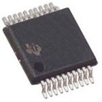
| 描述 | IC MCU 16BIT 8KB FLASH 20TVSOP16位微控制器 - MCU 16-Bit Ult-Lo-Pwr 8kB Flash 256B RAM |
| EEPROM容量 | - |
| 产品分类 | |
| I/O数 | 16 |
| 品牌 | Texas Instruments |
| 产品手册 | |
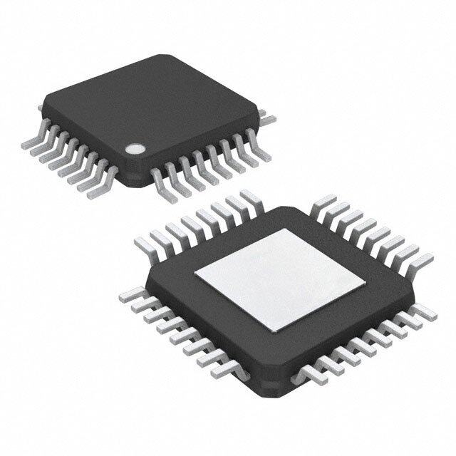
| 产品图片 |
|
| rohs | 符合RoHS无铅 / 符合限制有害物质指令(RoHS)规范要求 |
| 产品系列 | 嵌入式处理器和控制器,微控制器 - MCU,16位微控制器 - MCU,Texas Instruments MSP430F2131IDGVMSP430F2xx |
| 数据手册 | 点击此处下载产品Datasheethttp://www.ti.com/lit/pdf/slau144 |
| 产品型号 | MSP430F2131IDGV |
| RAM容量 | 256 x 8 |
| 产品培训模块 | http://www.digikey.cn/PTM/IndividualPTM.page?site=cn&lang=zhs&ptm=8361http://www.digikey.cn/PTM/IndividualPTM.page?site=cn&lang=zhs&ptm=8522http://www.digikey.cn/PTM/IndividualPTM.page?site=cn&lang=zhs&ptm=8576http://www.digikey.cn/PTM/IndividualPTM.page?site=cn&lang=zhs&ptm=8679http://www.digikey.cn/PTM/IndividualPTM.page?site=cn&lang=zhs&ptm=7557http://www.digikey.cn/PTM/IndividualPTM.page?site=cn&lang=zhs&ptm=25419http://www.digikey.cn/PTM/IndividualPTM.page?site=cn&lang=zhs&ptm=25427http://www.digikey.cn/PTM/IndividualPTM.page?site=cn&lang=zhs&ptm=25523http://www.digikey.cn/PTM/IndividualPTM.page?site=cn&lang=zhs&ptm=25524http://www.digikey.cn/PTM/IndividualPTM.page?site=cn&lang=zhs&ptm=25537http://www.digikey.cn/PTM/IndividualPTM.page?site=cn&lang=zhs&ptm=25788http://www.digikey.cn/PTM/IndividualPTM.page?site=cn&lang=zhs&ptm=25882http://www.digikey.cn/PTM/IndividualPTM.page?site=cn&lang=zhs&ptm=25885http://www.digikey.cn/PTM/IndividualPTM.page?site=cn&lang=zhs&ptm=26015http://www.digikey.cn/PTM/IndividualPTM.page?site=cn&lang=zhs&ptm=26006http://www.digikey.cn/PTM/IndividualPTM.page?site=cn&lang=zhs&ptm=30354 |
| 产品目录页面 | |
| 产品种类 | 16位微控制器 - MCU |
| 供应商器件封装 | 20-TVSOP |
| 其它名称 | 296-18116 |
| 制造商产品页 | http://www.ti.com/general/docs/suppproductinfo.tsp?distId=10&orderablePartNumber=MSP430F2131IDGV |
| 包装 | 托盘 |
| 单位重量 | 60.200 mg |
| 可编程输入/输出端数量 | 16 |
| 商标 | Texas Instruments |
| 商标名 | MSP430 |
| 处理器系列 | 2 Series |
| 外设 | 欠压检测/复位,POR,PWM,WDT |
| 安装风格 | SMD/SMT |
| 定时器数量 | 1 Timer |
| 封装 | Tube |
| 封装/外壳 | 20-TFSOP(0.173",4.40mm 宽) |
| 封装/箱体 | TVSOP-20 |
| 工作温度 | -40°C ~ 85°C |
| 工作电源电压 | 1.8 V to 3.6 V |
| 工厂包装数量 | 90 |
| 振荡器类型 | 内部 |
| 接口类型 | Timer UART |
| 数据RAM大小 | 256 B |
| 数据ROM大小 | 256 B |
| 数据Rom类型 | Flash |
| 数据总线宽度 | 16 bit |
| 数据转换器 | 斜率 A/D |
| 最大工作温度 | + 85 C |
| 最大时钟频率 | 16 MHz |
| 最小工作温度 | - 40 C |
| 标准包装 | 90 |
| 核心 | MSP430 |
| 核心处理器 | MSP430 |
| 核心尺寸 | 16-位 |
| 片上ADC | Yes |
| 电压-电源(Vcc/Vdd) | 1.8 V ~ 3.6 V |
| 程序存储器大小 | 8 kB |
| 程序存储器类型 | 闪存 |
| 程序存储容量 | 8KB(8K x 8 + 256B) |
| 系列 | MSP430F2131 |
| 输入/输出端数量 | 16 I/O |
| 连接性 | - |
| 速度 | 16MHz |


- 商务部:美国ITC正式对集成电路等产品启动337调查
- 曝三星4nm工艺存在良率问题 高通将骁龙8 Gen1或转产台积电
- 太阳诱电将投资9.5亿元在常州建新厂生产MLCC 预计2023年完工
- 英特尔发布欧洲新工厂建设计划 深化IDM 2.0 战略
- 台积电先进制程称霸业界 有大客户加持明年业绩稳了
- 达到5530亿美元!SIA预计今年全球半导体销售额将创下新高
- 英特尔拟将自动驾驶子公司Mobileye上市 估值或超500亿美元
- 三星加码芯片和SET,合并消费电子和移动部门,撤换高东真等 CEO
- 三星电子宣布重大人事变动 还合并消费电子和移动部门
- 海关总署:前11个月进口集成电路产品价值2.52万亿元 增长14.8%


PDF Datasheet 数据手册内容提取
MSP430F21x1 www.ti.com SLAS439F–SEPTEMBER2004–REVISEDAUGUST2011 MIXED SIGNAL MICROCONTROLLER FEATURES • SerialOnboardProgramming,NoExternal 1 ProgrammingVoltageNeeded,Programmable • LowSupplyVoltageRange:1.8Vto3.6V CodeProtectionbySecurityFuse • Ultra-LowPowerConsumption • BootstrapLoader – ActiveMode:250μAat1MHz,2.2V • OnChipEmulationModule – StandbyMode:0.7 μA • FamilyMembers: – OffMode(RAMRetention):0.1μA – MSP430F2101 • Ultra-FastWake-UpFromStandbyModein – 1KB+256BFlashMemory LessThan1μs – 128BRAM • 16-BitRISCArchitecture,62.5-nsInstruction CycleTime – MSP430F2111 • BasicClockModuleConfigurations – 2KB+256BFlashMemory – InternalFrequenciesupto16MHzWith – 128BRAM FourCalibratedFrequenciesto±1% – MSP430F2121 – 32-kHzCrystal – 4KB+256BFlashMemory – High-FrequencyCrystalupto16MHz – 256BRAM – Resonator – MSP430F2131 – ExternalDigitalClockSource – 8KB+256BFlashMemory • 16-BitTimer_AWithThreeCapture/Compare – 256BRAM Registers • Availableina20-PinPlasticSmall-Outline • On-ChipComparatorforAnalogSignal WideBody(SOWB)Package,20-PinPlastic CompareFunctionorSlopeAnalog-to-Digital Small-OutlineThin(TSSOP)Package,20-Pin (A/D)Conversion TVSOPPackage,and24-PinQFNPackage • BrownoutDetector • ForCompleteModuleDescriptions,Seethe MSP430x2xxFamilyUser’sGuide(SLAU144) DESCRIPTION The Texas Instruments MSP430 family of ultra-low-power microcontrollers consist of several devices featuring different sets of peripherals targeted for various applications. The architecture, combined with five low-power modes,isoptimizedtoachieveextendedbatterylifeinportablemeasurementapplications.Thedevicefeaturesa powerful 16-bit RISC CPU, 16-bit registers, and constant generators that contribute to maximum code efficiency.The digitally controlled oscillator (DCO) allows wake-up from low-power modes to active mode in less than1μs. The MSP430x21x1 series is an ultra-low-power mixed signal microcontroller with a built-in 16-bit timer, versatile analogcomparator,andsixteenI/Opins. Typical applications include sensor systems that capture analog signals, convert themto digital values, and then process the data for display or for transmission to a host system. Stand-alone RF sensor front end is another areaofapplication.TheanalogcomparatorprovidesslopeA/Dconversioncapability. 1 Pleasebeawarethatanimportantnoticeconcerningavailability,standardwarranty,anduseincriticalapplicationsofTexas Instrumentssemiconductorproductsanddisclaimerstheretoappearsattheendofthisdatasheet. PRODUCTIONDATAinformationiscurrentasofpublicationdate. Copyright©2004–2011,TexasInstrumentsIncorporated Products conform to specifications per the terms of the Texas Instruments standard warranty. Production processing does not necessarilyincludetestingofallparameters.
MSP430F21x1 SLAS439F–SEPTEMBER2004–REVISEDAUGUST2011 www.ti.com Table1.AvailableOptions PACKAGEDDEVICES T PLASTIC PLASTIC PLASTIC PLASTIC A 20-PINSOWB 20-PINTSSOP 20-PINTVSOP 24-PINQFN (DW) (PW) (DGV) (RGE) MSP430F2101IDW MSP430F2101IPW MSP430F2101IDGV MSP430F2101IRGE MSP430F2111IDW MSP430F2111IPW MSP430F2111IDGV MSP430F2111IRGE -40°Cto85°C MSP430F2121IDW MSP430F2121IPW MSP430F2121IDGV MSP430F2121IRGE MSP430F2131IDW MSP430F2131IPW MSP430F2131IDGV MSP430F2131IRGE MSP430F2101TDW MSP430F2101TPW MSP430F2101TDGV MSP430F2101TRGE MSP430F2111TDW MSP430F2111TPW MSP430F2111TDGV MSP430F2111TRGE -40°Cto105°C MSP430F2121TDW MSP430F2121TPW MSP430F2121TDGV MSP430F2121TRGE MSP430F2131TDW MSP430F2131TPW MSP430F2131TDGV MSP430F2131TRGE Development Tool Support All MSP430 microcontrollers include an Embedded Emulation Module (EEM) that allows advanced debugging andprogrammingthrougheasy-to-usedevelopmenttools.Recommendedhardwareoptionsinclude: • DebuggingandProgrammingInterfacewithTargetBoard – MSP-FET430U28(PWpackage) • DebuggingandProgrammingInterface – MSP-FET430UIF(USB) – MSP-FET430PIF(ParallelPort) • TargetBoard – MSP-TS430PW28(PWpackage) • ProductionProgrammer – MSP-GANG430 2 Copyright©2004–2011,TexasInstrumentsIncorporated
MSP430F21x1 www.ti.com SLAS439F–SEPTEMBER2004–REVISEDAUGUST2011 Device Pinout DW,PW,orDGVPACKAGE (TOPVIEW) TEST 1 20 P1.7/TA2/TDO/TDI V 2 19 P1.6/TA1/TDI/TCLK CC P2.5/CA5 3 18 P1.5/TA0/TMS V 4 17 P1.4/SMCLK/TCK SS XOUT/P2.7/CA7 5 16 P1.3/TA2 XIN/P2.6/CA6 6 15 P1.2/TA1 RST/NMI 7 14 P1.1/TA0 P2.0/ACLK/CA2 8 13 P1.0/TACLK P2.1/INCLK/CA3 9 12 P2.4/TA2/CA1 P2.2/CAOUT/TA0/CA4 10 11 P2.3/TA1/CA0 RGEPACKAGE (TOPVIEW) K DIL TC DO/DI/T TT A5 A2/A1/ C TT 5/ ST7/6/ P2.VCCTEP1.P1.NC 242322212019 NC 1 18 P1.5/TA0/TMS V 2 17 P1.4/SMCLK/TCK SS XOUT/P2.7/CA7 3 Exposed 16 P1.3/TA2 XIN/P2.6/CA6 4 Thermal Pad 15 P1.2/TA1 RST/NMI 5 14 P1.1/TA0 P2.0/ACLK/CA2 6 13 P1.0/TACLK 7 8 9 101112 34C01C AANAAN CC CC K/0/ 1/2/ LA AA CT TT NT/ 3/4/ 1/IOU P2.P2. 2.A PC 2/ 2. P A. NC=Notinternallyconnected B. ExposedthermalpadconnectiontoV recommended. SS Copyright©2004–2011,TexasInstrumentsIncorporated 3
MSP430F21x1 SLAS439F–SEPTEMBER2004–REVISEDAUGUST2011 www.ti.com Functional Block Diagram P2.x, VCC VSS P1.x, JTAG XIN/XOUT 8 8 XIN XOUT Port P1 Port P2 ACLK Flash RAM BasicClock Comparator System+ 8kB 256B _A+ 8I/O 8I/O SMCLK Interrupt Interrupt 4kB 256B 8 Channel capability, capability, 2kB 128B MCLK 1kB 128B InputMux pullup/down pullup/down resistors resistors MAB 16MHz CPU incl. 16 Registers MDB Emulation (2BP) Watchdog Timer_A3 JTAG Brownout WDT+ Interface Protection 3CC 15/16 Bit Registers RST/NMI NOTE: SeeportschematicssectionfordetailedI/Oinformation. 4 Copyright©2004–2011,TexasInstrumentsIncorporated
MSP430F21x1 www.ti.com SLAS439F–SEPTEMBER2004–REVISEDAUGUST2011 Table2.TerminalFunctions TERMINAL NO. DW, I/O DESCRIPTION NAME PW, RGE or DGV General-purposedigitalI/Opin P1.0/TACLK 13 13 I/O Timer_A,clocksignalTACLKinput General-purposedigitalI/Opin P1.1/TA 14 14 I/O Timer_A,capture:CCI0Ainput,compare:Out0output/BSLtransmit General-purposedigitalI/Opin P1.2/TA1 15 15 I/O Timer_A,capture:CCI1Ainput,compare:Out1output General-purposedigitalI/Opin P1.3/TA2 16 16 I/O Timer_A,capture:CCI2Ainput,compare:Out2output General-purposedigitalI/Opin/SMCLKsignaloutput P1.4/SMCLK/TCK 17 17 I/O TestClockinputfordeviceprogrammingandtest General-purposedigitalI/Opin/Timer_A,compare:Out0output P1.5/TA/TMS 18 18 I/O TestModeSelectinputfordeviceprogrammingandtest General-purposedigitalI/Opin/Timer_A,compare:Out1output P1.6/TA1/TDI/TCLK 19 20 I/O TestDataInputorTestClockInputforprogrammingandtest General-purposedigitalI/Opin/Timer_A,compare:Out2output P1.7/TA2/TDO/TDI(1) 20 21 I/O TestDataOutputorTestDataInputforprogrammingandtest General-purposedigitalI/Opin/ACLKoutput P2.0/ACLK/CA2 8 6 I/O Comparator_A+,CA2input General-purposedigitalI/Opin/Timer_A,clocksignalatINCLK P2.1/INCLK/CA3 9 7 I/O Comparator_A+,CA3input General-purposedigitalI/Opin P2.2/CAOUT/TA/CA4 10 8 I/O Timer_A,capture:CCI0Binput/BSLreceive Comparator_A+,output/CA4input General-purposedigitalI/Opin/Timer_A,compare:Out1output P2.3/CA0/TA1 11 10 I/O Comparator_A+,CA0input General-purposedigitalI/Opin/Timer_A,compare:Out2output P2.4/CA1/TA2 12 11 I/O Comparator_A+,CA1input General-purposedigitalI/Opin P2.5/CA5 3 24 I/O Comparator_A+,CA5input Inputterminalofcrystaloscillator XIN/P2.6/CA6 6 4 I/O General-purposedigitalI/Opin Comparator_A+,CA6input Outputterminalofcrystaloscillator XOUT/P2.7/CA7(2) 5 3 I/O General-purposedigitalI/Opin Comparator_A+,CA7input RST/NMI 7 5 I Resetornonmaskableinterruptinput SelectstestmodeforJTAGpinsonPort1.Thedeviceprotectionfuseisconnectedto TEST 1 22 I TEST. V 2 23 Supplyvoltage CC V 4 2 Groundreference SS QFNPad NA Pad NA QFNpackagethermalpad.ConnecttoV . SS (1) TDOorTDIisselectedviaJTAGinstruction. (2) IfXOUT/P2.7/CA7isusedasaninput,excesscurrentwillflowuntilP2SEL.7iscleared.Thisisduetotheoscillatoroutputdriver connectiontothispadafterreset. Copyright©2004–2011,TexasInstrumentsIncorporated 5
MSP430F21x1 SLAS439F–SEPTEMBER2004–REVISEDAUGUST2011 www.ti.com SHORT-FORM DESCRIPTION CPU Program Counter PC/R0 The MSP430™ CPU has a 16-bit RISC architecture Stack Pointer SP/R1 that is highly transparent to the application. All operations, other than program-flow instructions, are Status Register SR/CG1/R2 performed as register operations in conjunction with seven addressing modes for source operand and four Constant Generator CG2/R3 addressingmodesfordestinationoperand. General-Purpose Register R4 The CPU is integrated with 16 registers that provide reduced instruction execution time. The General-Purpose Register R5 register-to-register operation execution time is one cycleoftheCPUclock. General-Purpose Register R6 Four of the registers, R0 to R3, are dedicated as program counter, stack pointer, status register, and General-Purpose Register R7 constant generator respectively. The remaining registersaregeneral-purposeregisters. General-Purpose Register R8 Peripherals are connected to the CPU using data, General-Purpose Register R9 address, and control buses and can be handled with allinstructions. General-Purpose Register R10 Instruction Set General-Purpose Register R11 The instruction set consists of 51 instructions with General-Purpose Register R12 three formats and seven address modes. Each instruction can operate on word and byte data. General-Purpose Register R13 Table 3 shows examples of the three types of instruction formats; Table 4 shows the address General-Purpose Register R14 modes. General-Purpose Register R15 Table3.InstructionWordFormats INSTRUCTIONFORMAT EXAMPLE OPERATION Dualoperands,source-destination ADDR4,R5 R4+R5→R5 Singleoperands,destinationonly CALLR8 PC→(TOS),R8→PC Relativejump,unconditional/conditional JNE Jump-on-equalbit=0 Table4.AddressModeDescriptions ADDRESSMODE S(1) D(2) SYNTAX EXAMPLE OPERATION Register ✓ ✓ MOVRs,Rd MOVR10,R11 R10→R11 Indexed ✓ ✓ MOVX(Rn),Y(Rm) MOV2(R5),6(R6) M(2+R5)→M(6+R6) Symbolic(PCrelative) ✓ ✓ MOVEDE,TONI M(EDE)→M(TONI) Absolute ✓ ✓ MOV&MEM,&TCDAT M(MEM)→M(TCDAT) Indirect ✓ MOV@Rn,Y(Rm) MOV@R10,Tab(R6) M(R10)→M(Tab+R6) M(R10)→R11 Indirectautoincrement ✓ MOV@Rn+,Rm MOV@R10+,R11 R10+2→R10 Immediate ✓ MOV#X,TONI MOV#45,TONI #45→M(TONI) (1) S=source (2) D=destination 6 Copyright©2004–2011,TexasInstrumentsIncorporated
MSP430F21x1 www.ti.com SLAS439F–SEPTEMBER2004–REVISEDAUGUST2011 Operating Modes The MSP430 microcontrollers have one active mode and five software-selectable low-power modes of operation. An interrupt event can wake up the device from any of the five low-power modes, service the request, and restorebacktothelow-powermodeonreturnfromtheinterruptprogram. Thefollowingsixoperatingmodescanbeconfiguredbysoftware: • Activemode(AM) – Allclocksareactive. • Low-powermode0(LPM0) – CPUisdisabled. – ACLKandSMCLKremainactive.MCLKisdisabled. • Low-powermode1(LPM1) – CPUisdisabledACLKandSMCLKremainactive.MCLKisdisabled. – DCOdc-generatorisdisabledifDCOnotusedinactivemode. • Low-powermode2(LPM2) – CPUisdisabled. – MCLKandSMCLKaredisabled. – DCOdc-generatorremainsenabled. – ACLKremainsactive. • Low-powermode3(LPM3) – CPUisdisabled. – MCLKandSMCLKaredisabled. – DCOdc-generatorisdisabled. – ACLKremainsactive. • Low-powermode4(LPM4) – CPUisdisabled. – ACLKisdisabled. – MCLKandSMCLKaredisabled. – DCOdc-generatorisdisabled. – Crystaloscillatorisstopped. Copyright©2004–2011,TexasInstrumentsIncorporated 7
MSP430F21x1 SLAS439F–SEPTEMBER2004–REVISEDAUGUST2011 www.ti.com Interrupt Vector Addresses The interrupt vectors and the power-up starting address are located in the address range of 0xFFFF to 0xFFC0. Thevectorcontainsthe16-bitaddressoftheappropriateinterrupthandlerinstructionsequence. If the reset vector (located at address 0xFFFE) contains 0xFFFF (for example, if flash is not programmed), the CPUgoesintoLPM4immediatelyafterpowerup. Table5.InterruptVectorAddresses INTERRUPTSOURCE INTERRUPTFLAG SYSTEMINTERRUPT WORDADDRESS PRIORITY Power-up PORIFG Externalreset RSTIFG Watchdog WDTIFG Reset 0xFFFE 31,highest Flashkeyviolation KEYV(1) PCoutofrange(2) NMI NMIIFG (non)-maskable Oscillatorfault OFIFG (non)-maskable 0xFFFC 30 Flashmemoryaccessviolation ACCVIFG(1)(3) (non)-maskable 0xFFFA 29 0xFFF8 28 Comparator_A+ CAIFG maskable 0xFFF6 27 WatchdogTimer+ WDTIFG maskable 0xFFF4 26 Timer_A3 TACCR0CCIFG(4) maskable 0xFFF2 25 TACCR2,TACCR1CCIFG, Timer_A3 TAIFG(1)(4) maskable 0xFFF0 24 0xFFEE 23 0xFFEC 22 0xFFEA 21 0xFFE8 20 I/OportP2(eightflags) P2IFG.0toP2IFG.7(1)(4) maskable 0xFFE6 19 I/OportP1(eightflags) P1IFG.0toP1IFG.7(1)(4) maskable 0xFFE4 18 0xFFE2 17 0xFFE0 16 See (5) 0xFFDE 15 See (6) 0xFFDCto0xFFC0 14to0,lowest (1) Multiplesourceflags (2) AresetisgeneratediftheCPUtriestofetchinstructionsfromwithinthemoduleregistermemoryaddressrange(0x0000to0x01FF)or fromwithinunusedaddressrange. (3) (non)-maskable:theindividualinterrupt-enablebitcandisableaninterruptevent,butthegeneralinterruptenablecannot. (4) Interruptflagsarelocatedinthemodule. (5) Thislocationisusedasbootstraploadersecuritykey(BSLSKEY). Avalueof0xAA55atthislocationdisablestheBSLcompletely. Avalueof0x0disablestheerasureoftheflashifaninvalidpasswordissupplied. (6) Theinterruptvectorsataddresses0xFFDCto0xFFC0arenotusedinthisdeviceandcanbeusedforregularprogramcodeif necessary. 8 Copyright©2004–2011,TexasInstrumentsIncorporated
MSP430F21x1 www.ti.com SLAS439F–SEPTEMBER2004–REVISEDAUGUST2011 Special Function Registers Most interrupt and module enable bits are collected into the lowest address space. Special function register bits not allocated to a functional purpose are not physically present in the device. Simple software access is provided withthisarrangement. Legend rw Bitcanbereadandwritten. rw-0,1 Bitcanbereadandwritten.ItisResetorSetbyPUC. rw-(0),(1) Bitcanbereadandwritten.ItisResetorSetbyPOR. SFRbitisnotpresentindevice. Table6.InterruptEnable1 Address 7 6 5 4 3 2 1 0 00h ACCVIE NMIIE OFIE WDTIE rw-0 rw-0 rw-0 rw-0 WDTIE Watchdogtimerinterruptenable.Inactiveifwatchdogmodeisselected.Activeifwatchdogtimerisconfiguredininterval timermode. OFIE Oscillatorfaultinterruptenable NMIIE (Non)maskableinterruptenable ACCVIE Flashaccessviolationinterruptenable Table7.InterruptEnable2 Address 7 6 5 4 3 2 1 0 01h Table8.InterruptFlagRegister1 Address 7 6 5 4 3 2 1 0 02h NMIIFG RSTIFG PORIFG OFIFG WDTIFG rw-0 rw-(0) rw-(1) rw-1 rw-(0) WDTIFG Setonwatchdogtimeroverflow(inwatchdogmode)orsecuritykeyviolation. ResetonV power-uporaresetconditionatRST/NMIpininresetmode. CC OFIFG Flagsetonoscillatorfault RSTIFG Externalresetinterruptflag.SetonaresetconditionatRST/NMIpininresetmode.ResetonV powerup. CC PORIFG Power-onresetinterruptflag.SetonV powerup. CC NMIIFG SetviaRST/NMIpin Table9.InterruptFlagRegister2 Address 7 6 5 4 3 2 1 0 03h Copyright©2004–2011,TexasInstrumentsIncorporated 9
MSP430F21x1 SLAS439F–SEPTEMBER2004–REVISEDAUGUST2011 www.ti.com Memory Organization Table10.MemoryOrganization MSP430F2101 MSP430F2111 MSP430F2121 MSP430F2131 Memory Size 1KBFlash 2KBFlash 4KBFlash 8KBFlash Main:interruptvector Flash 0xFFFFto0xFFE0 0xFFFFto0xFFE0 0xFFFFto0xFFE0 0xFFFFto0xFFE0 Main:codememory Flash 0xFFFFto0xFC00 0xFFFFto0xF800 0xFFFFto0xF000 0xFFFFto0xE000 Informationmemory Size 256Byte 256Byte 256Byte 256Byte Flash 0x10FFto0x1000 0x10FFto0x1000 0x10FFto0x1000 0x10FFto0x1000 Bootmemory Size 1KB 1KB 1KB 1KB ROM 0x0FFFto0x0C00 0x0FFFto0x0C00 0x0FFFto0x0C00 0x0FFFto0x0C00 RAM Size 128B 128B 256Byte 256Byte 0x027Fto0x0200 0x027Fto0x0200 0x02FFto0x0200 0x02FFto0x0200 Peripherals 16-bit 0x01FFto0x0100 0x01FFto0x0100 0x01FFto0x0100 0x01FFto0x0100 8-bit 0x0FFto0x010 0x0FFto0x010 0x0FFto0x010 0x0FFto0x010 8-bitSFR 0x0Fto0x00 0x0Fto0x00 0x0Fto0x00 0x0Fto0x00 Bootstrap Loader (BSL) The MSP430 bootstrap loader (BSL) enables users to program the flash memory or RAM using a UART serial interface. Access to theMSP430memoryvia theBSLis protected by user-defined password.Abootstrap loader securitykeyisprovidedataddress0FFDEhtodisabletheBSLcompletelyortodisabletheerasureoftheflashif an invalid password is supplied. For complete description of the features of the BSL and its implementation, see theMSP430ProgrammingViatheBootstrapLoaderUser’sGuide,literaturenumberSLAU319. Table11.BSLKeys BSLKEY DESCRIPTION 00000h Erasureofflashdisabledifaninvalidpasswordissupplied 0AA55h BSLdisabled anyothervalue BSLenabled Table12.BSLFunctionPins BSLFUNCTION DW,PW,DGVPACKAGEPINS RGEPACKAGEPINS Datatransmit 14-P1.1 14-P1.1 Datareceive 10-P2.2 8-P2.2 Flash Memory The flash memory can be programmed via the JTAG port, the bootstrap loader, or in-system by the CPU. The CPUcanperformsingle-byteandsingle-wordwritestotheflashmemory.Featuresoftheflashmemoryinclude: • Flash memory has n segments of main memory and four segments of information memory (A to D) of 64byteseach.Eachsegmentinmainmemoryis512bytesinsize. • Segments0tonmaybeerasedinonestep,oreachsegmentmaybeindividuallyerased. • SegmentsAtoDcanbeerasedindividually,orasagroupwithsegments0ton. SegmentsAtoDarealsocalledinformationmemory. • Segment A contains calibration data. After reset, segment A is protected against programming and erasing. It can be unlocked, but care should be taken not to erase this segment if the device-specific calibration data is required. 10 Copyright©2004–2011,TexasInstrumentsIncorporated
MSP430F21x1 www.ti.com SLAS439F–SEPTEMBER2004–REVISEDAUGUST2011 Peripherals Peripherals are connected to the CPU through data, address, and control buses and can be handled using all instructions.Forcompletemoduledescriptions,seetheMSP430x2xxFamilyUser'sGuide(SLAU144). Oscillator and System Clock The clock system is supported by the basic clock module that includes support for a 32768-Hz watch crystal oscillator, an internal digitally-controlled oscillator (DCO), and a high-frequency crystal oscillator. The basic clock module is designed to meet the requirements of both low system cost and low power consumption. The internal DCO provides a fast turn-on clock source and stabilizes in less than 1 µs. The basic clock module provides the followingclocksignals: • Auxiliaryclock(ACLK),sourcedfroma32768-Hzwatchcrystalorahigh-frequencycrystal • Mainclock(MCLK),thesystemclockusedbytheCPU • Sub-Mainclock(SMCLK),thesub-systemclockusedbytheperipheralmodules Table13.DCOCalibrationData,ProvidedFromFactoryInFlashInfoMemory SegmentA DCOFREQUENCY CALIBRATIONREGISTER SIZE ADDRESS CALBC1_1MHZ byte 0x010FF 1MHz CALBC0_1MHZ byte 0x010FE CALBC1_8MHZ byte 0x010FD 8MHz CALBC0_8MHZ byte 0x010FC CALBC1_12MHZ byte 0x010FB 12MHz CALBC0_12MHZ byte 0x010FA CALBC1_16MHZ byte 0x010F9 16MHz CALBC0_16MHZ byte 0x010F8 Brownout The brownout circuit is implemented to provide the proper internal reset signal to the device during power on and poweroff. Digital I/O Therearetwo8-bitI/Oportsimplemented—portsP1andP2. • AllindividualI/Obitsareindependentlyprogrammable. • Anycombinationofinput,output,andinterruptconditionispossible. • Edge-selectableinterruptinputcapabilityforalleightbitsofportP1andP2. • Read/writeaccesstoport-controlregistersissupportedbyallinstructions. • EachI/Ohasanindividuallyprogrammablepullup/pulldownresistor. Watchdog Timer (WDT+) The primary function of the WDT+ module is to perform a controlled system restart after a software problem occurs. If the selected time interval expires, a system reset is generated. If the watchdog function is not needed in an application, the module can be disabled or configured as an interval timer and can generate interrupts at selectedtimeintervals. Comparator_A+ The primary function of the comparator_A+ module is to support precision slope analog-to-digital conversions, battery-voltagesupervision,andmonitoringofexternalanalogsignals. Copyright©2004–2011,TexasInstrumentsIncorporated 11
MSP430F21x1 SLAS439F–SEPTEMBER2004–REVISEDAUGUST2011 www.ti.com Timer_A3 Timer_A3 is a 16-bit timer/counter with three capture/compare registers. Timer_A3 can support multiple capture/compares, PWM outputs, and interval timing. Timer_A3 also has extensive interrupt capabilities. Interrupts may be generated from the counter on overflow conditions and from each of the capture/compare registers. Table14.Timer_A3SignalConnections INPUTPINNUMBER MODULE OUTPUTPINNUMBER DEVICEINPUT MODULE MODULE OUTPUT DW,PW,DGV RGE SIGNAL INPUTNAME BLOCK SIGNAL DW,PW,DGV RGE 13-P1.0 13-P1.0 TACLK TACLK ACLK ACLK Timer NA SMCLK SMCLK 9-P2.1 7-P2.1 INCLK INCLK 14-P1.1 14-P1.1 TA CCI0A 14-P1.1 14-P1.1 10-P2.2 8-P2.2 TA CCI0B 18-P1.5 18-P1.5 CCR0 TA VSS GND VCC VCC 15-P1.2 15-P1.2 TA1 CCI1A 11-P2.3 10-P2.3 CAOUT CCI1B 15-P1.2 15-P1.2 (internal) CCR1 TA1 VSS GND 19-P1.6 20-P1.6 VCC VCC 16-P1.3 16-P1.3 TA2 CCI2A 12-P2.4 11-P2.4 ACLK(internal) CCI2B 16-P1.3 16-P1.3 CCR2 TA2 VSS GND 20-P1.7 21-P1.7 VCC VCC 12 Copyright©2004–2011,TexasInstrumentsIncorporated
MSP430F21x1 www.ti.com SLAS439F–SEPTEMBER2004–REVISEDAUGUST2011 Peripheral File Map Table15.PeripheralsWithWordAccess MODULE REGISTERNAME SHORTNAME ADDRESSOFFSET Timer_A Capture/compareregister TACCR2 0x0176 Capture/compareregister TACCR1 0x0174 Capture/compareregister TACCR0 0x0172 Timer_A3register TAR 0x0170 Capture/comparecontrol TACCTL2 0x0166 Capture/comparecontrol TACCTL1 0x0164 Capture/comparecontrol TACCTL0 0x0162 Timer_A3control TACTL 0x0160 Timer_A3interruptvector TAIV 0x012E FlashMemory Flashcontrol3 FCTL3 0x012C Flashcontrol2 FCTL2 0x012A Flashcontrol1 FCTL1 0x0128 WatchdogTimer+ Watchdog/timercontrol WDTCTL 0x0120 Table16.PeripheralsWithByteAccess MODULE REGISTERNAME SHORTNAME ADDRESSOFFSET Comparator_A+ Comparator_Aportdisable CAPD 0x005B Comparator_Acontrol2 CACTL2 0x005A Comparator_Acontrol1 CACTL1 0x0059 BasicClock Basicclocksystemcontrol3 BCSCTL3 0x0053 Basicclocksystemcontrol2 BCSCTL2 0x0058 Basicclocksystemcontrol1 BCSCTL1 0x0057 DCOclockfrequencycontrol DCOCTL 0x0056 PortP2 PortP2resistorenable P2REN 0x002F PortP2selection P2SEL 0x002E PortP2interruptenable P2IE 0x002D PortP2interruptedgeselect P2IES 0x002C PortP2interruptflag P2IFG 0x002B PortP2direction P2DIR 0x002A PortP2output P2OUT 0x0029 PortP2input P2IN 0x0028 PortP1 PortP1resistorenable P1REN 0x0027 PortP1selection P1SEL 0x0026 PortP1interruptenable P1IE 0x0025 PortP1interruptedgeselect P1IES 0x0024 PortP1interruptflag P1IFG 0x0023 PortP1direction P1DIR 0x0022 PortP1output P1OUT 0x0021 PortP1input P1IN 0x0020 SpecialFunction SFRinterruptflag2 IFG2 0x0003 SFRinterruptflag1 IFG1 0x0002 SFRinterruptenable2 IE2 0x0001 SFRinterruptenable1 IE1 0x0000 Copyright©2004–2011,TexasInstrumentsIncorporated 13
MSP430F21x1 SLAS439F–SEPTEMBER2004–REVISEDAUGUST2011 www.ti.com Absolute Maximum Ratings(1) VoltageappliedatV toV -0.3Vto4.1V CC SS Voltageappliedtoanypin (2) -0.3Vto(V +0.3V) CC Diodecurrentatanydeviceterminal ±2mA Unprogrammeddevice -55°Cto150°C Storagetemperature,T (3) stg Programmeddevice -55°Cto150°C (1) Stressesbeyondthoselistedunderabsolutemaximumratingsmaycausepermanentdamagetothedevice.Thesearestressratings only,andfunctionaloperationofthedeviceattheseoranyotherconditionsbeyondthoseindicatedunderrecommendedoperating conditionsisnotimplied.Exposuretoabsolute-maximum-ratedconditionsforextendedperiodsmayaffectdevicereliability. (2) AllvoltagesreferencedtoV .TheJTAGfuse-blowvoltage,V ,isallowedtoexceedtheabsolutemaximumrating.Thevoltageis SS FB appliedtotheTESTpinwhenblowingtheJTAGfuse. (3) HighertemperaturemaybeappliedduringboardsolderingprocessaccordingtothecurrentJEDECJ-STD-020specificationwithpeak reflowtemperaturesnothigherthanclassifiedonthedevicelabelontheshippingboxesorreels. Recommended Operating Conditions(1) MIN NOM MAX UNIT Duringprogramexecution 1.8 3.6 V Supplyvoltage,AV =DV =V V CC CC CC CC Duringflashmemoryprogramming 2.2 3.6 V Supplyvoltage,AV =DV =V 0 V SS SS SS SS Iversion -40 85 T Operatingfree-airtemperature °C A Tversion -40 105 V =1.8V,Dutycycle=50%±10% 0 6 Processorfrequency(maximumMCLK CC f frequency)(2)(1) V =2.7V,Dutycycle=50%±10% 0 12 MHz SYSTEM CC (seeFigure1) V ≥3.3V,Dutycycle=50%±10% 0 16 CC (1) Modulesmighthaveadifferentmaximuminputclockspecification.Seethespecificationoftherespectivemoduleinthisdatasheet. (2) TheMSP430CPUisclockeddirectlywithMCLK.BoththehighandlowphaseofMCLKmustnotexceedthepulsewidthofthe specifiedmaximumfrequency. Legend: 16MHz Supply voltage range during flash memory z H programming M − 12MHz y c n e Supply voltage range u q during program execution e Fr m e 6MHz st y S 1.8V 2.2V 2.7V 3.3V 3.6V Supply Voltage−V NOTE: Minimumprocessorfrequencyisdefinedbysystemclock.FlashprogramoreraseoperationsrequireaminimumV CC of2.2V. Figure1. OperatingArea 14 Copyright©2004–2011,TexasInstrumentsIncorporated
MSP430F21x1 www.ti.com SLAS439F–SEPTEMBER2004–REVISEDAUGUST2011 Active Mode Supply Current (into DV + AV ) Excluding External Current CC CC overrecommendedrangesofsupplyvoltageandoperatingfree-airtemperature(unlessotherwisenoted)(1)(2) PARAMETER TESTCONDITIONS T V MIN TYP MAX UNIT A CC f =f =f =1MHz, 2.2V 250 300 DCO MCLK SMCLK f =32768Hz, ACLK Programexecutesinflash, Activemode(AM) I BCSCTL1=CALBC1_1MHZ, µA AM,1MHz current(1MHz) DCOCTL=CALDCO_1MHZ, 3V 350 410 CPUOFF=0,SCG0=0,SCG1=0, OSCOFF=0 f =f =f =1MHz, 2.2V 200 DCO MCLK SMCLK f =32768Hz, ACLK ProgramexecutesinRAM, Activemode(AM) I BCSCTL1=CALBC1_1MHZ, µA AM,1MHz current(1MHz) DCOCTL=CALDCO_1MHZ, 3V 300 CPUOFF=0,SCG0=0,SCG1=0, OSCOFF=0 f =f =f =32768Hz/8 -40°Cto85°C 2 5 MCLK SMCLK ACLK =4096Hz, 2.2V 105°C 6 f =0Hz, DCO Activemode(AM) Programexecutesinflash, -40°Cto85°C 3 9 I µA AM,4kHz current(4kHz) SELMx=11,SELS=1, DIVMx=DIVSx=DIVAx=11, 3V CPUOFF=0,SCG0=1,SCG1=0, 105°C 9 OSCOFF=0 f =f =f ≈100kHz, 2.2V 60 85 MCLK SMCLK DCO(0,0) f =0Hz, Activemode(AM) ACLK I Programexecutesinflash, µA AM,100kHz current(100kHz) RSELx=0,DCOx=0,CPUOFF=0, 3V 72 95 SCG0=0,SCG1=0,OSCOFF=1 (1) Allinputsaretiedto0VorV .Outputsdonotsourceorsinkanycurrent. CC (2) ThecurrentsarecharacterizedwithaMicroCrystalCC4V-T1ASMDcrystalwithaloadcapacitanceof9pF.Theinternalandexternal loadcapacitanceischosentocloselymatchtherequired9pF. Typical Characteristics - Active-Mode Supply Current (Into V ) CC ACTIVE-MODECURRENT vs ACTIVE-MODECURRENT SUPPLYVOLTAGE vs T =25°C DCOFREQUENCY A 7.0 5.0 f = 16 MHz 6.0 DCO mA 5.0 f = 12 MHz mA 4.0 TA= 85°C – DCO – T = 25°C Current 4.0 Current 3.0 A ode 3.0 fDCO= 8 MHz Mode VCC= 3 V M e 2.0 e v T = 85°C Activ 2.0 Acti TAA= 25°C 1.0 1.0 VCC= 2.2 V f = 1 MHz DCO 0.0 0.0 1.5 2.0 2.5 3.0 3.5 4.0 0 4 8 12 16 VCC–Supply Voltage–V fDCO–DCO Frequency–MHz Figure2. Figure3. Copyright©2004–2011,TexasInstrumentsIncorporated 15
MSP430F21x1 SLAS439F–SEPTEMBER2004–REVISEDAUGUST2011 www.ti.com Low-Power-Mode Supply Currents (Into V ) Excluding External Current (1)(2) CC overrecommendedrangesofsupplyvoltageandoperatingfree-airtemperature(unlessotherwisenoted) PARAMETER TESTCONDITIONS T V MIN TYP MAX UNIT A CC f =0MHz, 2.2V 65 80 MCLK f =f =1MHz, SMCLK DCO f =32768Hz, Low-powermode0 ACLK ILPM0,1MHz (LPM0)current(3) BDCCSOCCTTLL1==CCAALLDBCCO1__11MMHHZZ,, 3V 85 100 µA CPUOFF=1,SCG0=0,SCG1=0, OSCOFF=0 f =0MHz, 2.2V 37 48 MCLK f =f (0,0)≈100kHz, SMCLK DCO Low-powermode0 f =0Hz, ILPM0,100kHz (LPM0)current(3) RASCLEKLx=0,DCOx=0, 3V 41 52 µA CPUOFF=1,SCG0=0,SCG1=0, OSCOFF=1 f =f =0MHz, -40°Cto85°C 22 29 MCLK SMCLK f =1MHz,f =32768Hz, 2.2V DCO ACLK 105°C 31 Low-powermode2 BCSCTL1=CALBC1_1MHZ, ILPM2 (LPM2)current(4) DCOCTL=CALDCO_1MHZ, -40°Cto85°C 25 32 µA CPUOFF=1,SCG0=0,SCG1=1, 3V OSCOFF=0 105°C 34 -40°C 0.7 1.2 25°C 0.7 1 2.2V 85°C 1.6 2.3 f =f =f =0MHz, DCO MCLK SMCLK Low-powermode3 f =32768Hz, 105°C 3 6 ILPM3,LFXT1 (LPM3)current(4) CAPCLUKOFF=1,SCG0=1,SCG1=1, -40°C 0.9 1.2 µA OSCOFF=0 25°C 0.9 1.2 3V 85°C 1.6 2.8 105°C 3 7 -40°C 0.1 0.5 f =f =f =0MHz, DCO MCLK SMCLK Low-powermode4 f =0Hz, 25°C 0.1 0.5 ILPM4 (LPM4)current(5) CAPCLUKOFF=1,SCG0=1,SCG1=1, 85°C 2.2V/3V 0.8 1.9 µA OSCOFF=1 105°C 2 4 (1) Allinputsaretiedto0VorV .Outputsdonotsourceorsinkanycurrent. CC (2) ThecurrentsarecharacterizedwithaMicroCrystalCC4V-T1ASMDcrystalwithaloadcapacitanceof9pF.Theinternalandexternal loadcapacitanceischosentocloselymatchtherequired9pF. (3) CurrentforbrownoutandWDTclockedbySMCLKincluded. (4) CurrentforbrownoutandWDTclockedbyACLKincluded. (5) Currentforbrownoutincluded. 16 Copyright©2004–2011,TexasInstrumentsIncorporated
MSP430F21x1 www.ti.com SLAS439F–SEPTEMBER2004–REVISEDAUGUST2011 Schmitt-Trigger Inputs (Ports P1, P2) overrecommendedrangesofsupplyvoltageandoperatingfree-airtemperature(unlessotherwisenoted) PARAMETER TESTCONDITIONS V MIN TYP MAX UNIT CC 0.45V 0.75V CC CC V Positive-goinginputthresholdvoltage 2.2V 1 1.65 V IT+ 3V 1.35 2.25 0.25V 0.55V CC CC V Negative-goinginputthresholdvoltage 2.2V 0.55 1.20 V IT- 3V 0.75 1.65 2.2V 0.2 1 V Inputvoltagehysteresis(V -V ) V hys IT+ IT- 3V 0.3 1 Forpullup:V =V , R Pullup/pulldownresistor IN SS 20 35 50 kΩ Pull Forpulldown:V =V IN CC C Inputcapacitance V =V orV 5 pF I IN SS CC Inputs (Ports P1, P2) overrecommendedrangesofsupplyvoltageandoperatingfree-airtemperature(unlessotherwisenoted) PARAMETER TESTCONDITIONS V MIN MAX UNIT CC PortP1,P2:P1.xtoP2.x,Externaltriggerpulsewidthto t(int) Externalinterrupttiming setinterruptflag(1) 2.2V/3V 20 ns (1) Anexternalsignalsetstheinterruptflageverytimetheminimuminterruptpulsewidtht ismet.Itmaybesetwithtriggersignals (int) shorterthant . (int) Leakage Current (Ports P1, P2) overrecommendedrangesofsupplyvoltageandoperatingfree-airtemperature(unlessotherwisenoted) PARAMETER TESTCONDITIONS V MIN MAX UNIT CC I High-impedanceleakagecurrent (1) (2) 2.2V/3V ±50 nA lkg(Px.y) (1) TheleakagecurrentismeasuredwithV orV appliedtothecorrespondingpin(s),unlessotherwisenoted. SS CC (2) Theleakageofthedigitalportpinsismeasuredindividually.Theportpinisselectedforinputandthepullup/pulldownresistoris disabled. Copyright©2004–2011,TexasInstrumentsIncorporated 17
MSP430F21x1 SLAS439F–SEPTEMBER2004–REVISEDAUGUST2011 www.ti.com Outputs (Ports P1, P2) overrecommendedrangesofsupplyvoltageandoperatingfree-airtemperature(unlessotherwisenoted) PARAMETER TESTCONDITIONS V MIN MAX UNIT CC I =-1.5mA(1) V -0.25 V OH(max) CC CC 2.2V I =-6mA(2) V -0.6 V OH(max) CC CC V High-leveloutputvoltage V OH I =-1.5mA(1) V -0.25 V OH(max) CC CC 3V I =-6mA(2) V -0.6 V OH(max) CC CC I =1.5mA(1) V V +0.25 OL(max) SS SS 2.2V I =6mA(2) V V +0.6 OL(max) SS SS V Low-leveloutputvoltage V OL I =1.5mA(1) V V +0.25 OL(max) SS SS 3V I =6mA(2) V V +0.6 OL(max) SS SS (1) Themaximumtotalcurrent,I andI ,foralloutputscombined,shouldnotexceed±12mAtoholdthemaximumvoltagedrop OH(max) OL(max) specified. (2) Themaximumtotalcurrent,I andI ,foralloutputscombined,shouldnotexceed±48mAtoholdthemaximumvoltagedrop OH(max) OL(max) specified. Output Frequency (Ports P1, P2) overrecommendedrangesofsupplyvoltageandoperatingfree-airtemperature(unlessotherwisenoted) PARAMETER TESTCONDITIONS V MIN MAX UNIT CC 2.2V 10 f Portoutputfrequency(withload) P1.4/SMCLK,C =20pF,R =1kΩ(1)(2) MHz Px.y L L 3V 12 2.2V 12 f Clockoutputfrequency P2.0/ACLK,P1.4/SMCLK,C =20pF(2) MHz Port_CLK L 3V 16 (1) Alternatively,aresistivedividerwithtwo0.5-kΩresistorsbetweenV andV isusedasload.Theoutputisconnectedtothecenter CC SS tapofthedivider. (2) Theoutputvoltagereachesatleast10%and90%V atthespecifiedtogglefrequency. CC 18 Copyright©2004–2011,TexasInstrumentsIncorporated
MSP430F21x1 www.ti.com SLAS439F–SEPTEMBER2004–REVISEDAUGUST2011 Typical Characteristics - Outputs Oneoutputloadedatatime. TYPICALLOW-LEVELOUTPUTCURRENT TYPICALLOW-LEVELOUTPUTCURRENT vs vs LOW-LEVELOUTPUTVOLTAGE LOW-LEVELOUTPUTVOLTAGE 25.0 50.0 VCC= 2.2 V TA= 25°C VCC= 3 V mA P2.4 mA P2.4 TA= 25°C nt− 20.0 TA= 85°C nt− 40.0 e e Curr Curr TA= 85°C put 15.0 put 30.0 ut ut O O el el ev ev w-L 10.0 w-L 20.0 o o L L al al Typic 5.0 Typic 10.0 − − OL OL I I 0.0 0.0 0.0 0.5 1.0 1.5 2.0 2.5 0.0 0.5 1.0 1.5 2.0 2.5 3.0 3.5 VOL−Low-Level Output Voltage−V VOL−Low-Level Output Voltage−V Figure4. Figure5. TYPICALHIGH-LEVELOUTPUTCURRENT TYPICALHIGH-LEVELOUTPUTCURRENT vs vs HIGH-LEVELOUTPUTVOLTAGE HIGH-LEVELOUTPUTVOLTAGE 0.0 0.0 VCC= 2.2 V VCC= 3 V A P2.4 A P2.4 m m − − nt −5.0 nt −10.0 e e urr urr C C ut ut p −10.0 p −20.0 ut ut O O el el v v e e h-L −15.0 h-L −30.0 g g Hi Hi al al ypic −20.0 ypic −40.0 TA= 85°C −T TA= 85°C −T H H O O I −25.0 TA= 25°C I −50.0 TA= 25°C 0.0 0.5 1.0 1.5 2.0 2.5 0.0 0.5 1.0 1.5 2.0 2.5 3.0 3.5 VOH−High-Level Output Voltage−V VOH−High-Level Output Voltage−V Figure6. Figure7. Copyright©2004–2011,TexasInstrumentsIncorporated 19
MSP430F21x1 SLAS439F–SEPTEMBER2004–REVISEDAUGUST2011 www.ti.com POR/Brownout Reset (BOR)(1)(2) overrecommendedrangesofsupplyvoltageandoperatingfree-airtemperature(unlessotherwisenoted) PARAMETER TESTCONDITIONS T V MIN TYP MAX UNIT A CC 0.7× V SeeFigure8 dV /dt≤3V/s V CC(start) CC V (B_IT-) SeeFigure8through V dV /dt≤3V/s 1.71 V (B_IT-) Figure10 CC -40°Cto85°C 70 130 180 V SeeFigure8 dV /dt≤3V/s mV hys(B_IT-) CC 105°C 70 130 210 t SeeFigure8 2000 µs d(BOR) Pulselengthneededat t RST/NMIpintoaccepted 2.2V/3V 2 µs (reset) resetinternally (1) ThecurrentconsumptionofthebrownoutmoduleisalreadyincludedintheI currentconsumptiondata.Thevoltagelevel CC V +V is≤1.8V. (B_IT-) hys(B_IT-) (2) Duringpowerup,theCPUbeginscodeexecutionfollowingaperiodoft afterV =V +V .ThedefaultDCOsettings d(BOR) CC (B_IT-) hys(B_IT-) mustnotbechangeduntilV ≥V ,whereV istheminimumsupplyvoltageforthedesiredoperatingfrequency. CC CC(min) CC(min) V CC V hys(B_IT−) V (B_IT−) VCC(start) 1 0 td(BOR) Figure8. POR/BrownoutReset(BOR)vsSupplyVoltage 20 Copyright©2004–2011,TexasInstrumentsIncorporated
MSP430F21x1 www.ti.com SLAS439F–SEPTEMBER2004–REVISEDAUGUST2011 Typical Characteristics - POR/Brownout Reset (BOR) 2 VCC tpw 3 V VCC= 3 V Typical Conditions V 1.5 − p) dro 1 C( C VCC(drop) V 0.5 0 0.001 1 1000 1 ns 1 ns tpw−Pulse Width− µs tpw−Pulse Width− µs Figure9.V LevelWithaSquareVoltageDroptoGenerateaPOR/BrownoutSignal CC(drop) VCC tpw 2 3 V VCC= 3 V V 1.5 Typical Conditions − p) o dr 1 C( C VCC(drop) V 0.5 tf=tr 0 0.001 1 1000 tf tr tpw−Pulse Width− µs tpw−Pulse Width− µs Figure10.V LevelWithaTriangleVoltageDroptoGenerateaPOR/BrownoutSignal CC(drop) Copyright©2004–2011,TexasInstrumentsIncorporated 21
MSP430F21x1 SLAS439F–SEPTEMBER2004–REVISEDAUGUST2011 www.ti.com Main DCO Characteristics • All ranges selected by RSELx overlap with RSELx + 1: RSELx = 0 overlaps RSELx = 1, ... RSELx = 14 overlapsRSELx=15. • DCOcontrolbitsDCOxhaveastepsizeasdefinedbyparameterS . DCO • Modulation control bits MODx select how often f is used within the period of 32 DCOCLK DCO(RSEL,DCO+1) cycles.Thefrequencyf isusedfortheremainingcycles.Thefrequencyisanaverageequalto: DCO(RSEL,DCO) 32×fDCO(RSEL,DCO) ×fDCO(RSEL,DCO+1) faverage = MOD×fDCO(RSEL,DCO) +(32–MOD)×fDCO(RSEL,DCO+1) DCO Frequency overrecommendedrangesofsupplyvoltageandoperatingfree-airtemperature(unlessotherwisenoted) PARAMETER TESTCONDITIONS V MIN TYP MAX UNIT CC RSELx<14 1.8 3.6 V Supplyvoltagerange RSELx=14 2.2 3.6 V CC RSELx=15 3.0 3.6 f DCOfrequency(0,0) RSELx=0,DCOx=0,MODx=0 2.2V/3V 0.06 0.14 MHz DCO(0,0) f DCOfrequency(0,3) RSELx=0,DCOx=3,MODx=0 2.2V/3V 0.07 0.17 MHz DCO(0,3) f DCOfrequency(1,3) RSELx=1,DCOx=3,MODx=0 2.2V/3V 0.10 0.20 MHz DCO(1,3) f DCOfrequency(2,3) RSELx=2,DCOx=3,MODx=0 2.2V/3V 0.14 0.28 MHz DCO(2,3) f DCOfrequency(3,3) RSELx=3,DCOx=3,MODx=0 2.2V/3V 0.20 0.40 MHz DCO(3,3) f DCOfrequency(4,3) RSELx=4,DCOx=3,MODx=0 2.2V/3V 0.28 0.54 MHz DCO(4,3) f DCOfrequency(5,3) RSELx=5,DCOx=3,MODx=0 2.2V/3V 0.39 0.77 MHz DCO(5,3) f DCOfrequency(6,3) RSELx=6,DCOx=3,MODx=0 2.2V/3V 0.54 1.06 MHz DCO(6,3) f DCOfrequency(7,3) RSELx=7,DCOx=3,MODx=0 2.2V/3V 0.80 1.50 MHz DCO(7,3) f DCOfrequency(8,3) RSELx=8,DCOx=3,MODx=0 2.2V/3V 1.10 2.10 MHz DCO(8,3) f DCOfrequency(9,3) RSELx=9,DCOx=3,MODx=0 2.2V/3V 1.60 3.00 MHz DCO(9,3) f DCOfrequency(10,3) RSELx=10,DCOx=3,MODx=0 2.2V/3V 2.50 4.30 MHz DCO(10,3) f DCOfrequency(11,3) RSELx=11,DCOx=3,MODx=0 2.2V/3V 3.00 5.50 MHz DCO(11,3) f DCOfrequency(12,3) RSELx=12,DCOx=3,MODx=0 2.2V/3V 4.30 7.30 MHz DCO(12,3) f DCOfrequency(13,3) RSELx=13,DCOx=3,MODx=0 2.2V/3V 6.00 9.60 MHz DCO(13,3) f DCOfrequency(14,3) RSELx=14,DCOx=3,MODx=0 2.2V/3V 8.60 13.9 MHz DCO(14,3) f DCOfrequency(15,3) RSELx=15,DCOx=3,MODx=0 3V 12.0 18.5 MHz DCO(15,3) f DCOfrequency(15,7) RSELx=15,DCOx=7,MODx=0 3V 16.0 26.0 MHz DCO(15,7) Frequencystepbetween S S =f /f 2.2V/3V 1.55 ratio RSEL rangeRSELandRSEL+1 RSEL DCO(RSEL+1,DCO) DCO(RSEL,DCO) Frequencystepbetweentap S S =f /f 2.2V/3V 1.05 1.08 1.12 ratio DCO DCOandDCO+1 DCO DCO(RSEL,DCO+1) DCO(RSEL,DCO) Dutycycle MeasuredatP1.4/SMCLK 2.2V/3V 40 50 60 % 22 Copyright©2004–2011,TexasInstrumentsIncorporated
MSP430F21x1 www.ti.com SLAS439F–SEPTEMBER2004–REVISEDAUGUST2011 Calibrated DCO Frequencies - Tolerance at Calibration overrecommendedrangesofsupplyvoltageandoperatingfree-airtemperature(unlessotherwisenoted) PARAMETER TESTCONDITIONS T V MIN TYP MAX UNIT A CC Frequencytoleranceatcalibration 25°C 3V -1 ±0.2 +1 % BCSCTL1=CALBC1_1MHZ, f 1-MHzcalibrationvalue DCOCTL=CALDCO_1MHZ, 25°C 3V 0.990 1 1.010 MHz CAL(1MHz) Gatingtime:5ms BCSCTL1=CALBC1_8MHZ, f 8-MHzcalibrationvalue DCOCTL=CALDCO_8MHZ, 25°C 3V 7.920 8 8.080 MHz CAL(8MHz) Gatingtime:5ms BCSCTL1=CALBC1_12MHZ, f 12-MHzcalibrationvalue DCOCTL=CALDCO_12MHZ, 25°C 3V 11.88 12 12.12 MHz CAL(12MHz) Gatingtime:5ms BCSCTL1=CALBC1_16MHZ, f 16-MHzcalibrationvalue DCOCTL=CALDCO_16MHZ, 25°C 3V 15.84 16 16.16 MHz CAL(16MHz) Gatingtime:2ms Calibrated DCO Frequencies - Tolerance Over Temperature 0°C to 85°C overrecommendedrangesofsupplyvoltageandoperatingfree-airtemperature(unlessotherwisenoted) PARAMETER TESTCONDITIONS T V MIN TYP MAX UNIT A CC 1-MHztoleranceover 0°Cto85°C 3V -2.5 ±0.5 +2.5 % temperature 8-MHztoleranceover 0°Cto85°C 3V -2.5 ±1 +2.5 % temperature 12-MHztoleranceover 0°Cto85°C 3V -2.5 ±1 +2.5 % temperature 16-MHztoleranceover 0°Cto85°C 3V -3 ±2 +3 % temperature 2.2V 0.97 1 1.03 BCSCTL1=CALBC1_1MHZ, f 1-MHzcalibrationvalue DCOCTL=CALDCO_1MHZ, 0°Cto85°C 3V 0.975 1 1.025 MHz CAL(1MHz) Gatingtime:5ms 3.6V 0.97 1 1.03 2.2V 7.76 8 8.4 BCSCTL1=CALBC1_8MHZ, f 8-MHzcalibrationvalue DCOCTL=CALDCO_8MHZ, 0°Cto85°C 3V 7.8 8 8.2 MHz CAL(8MHz) Gatingtime:5ms 3.6V 7.6 8 8.24 2.2V 11.7 12 12.3 BCSCTL1=CALBC1_12MHZ, f 12-MHzcalibrationvalue DCOCTL=CALDCO_12MHZ, 0°Cto85°C 3V 11.7 12 12.3 MHz CAL(12MHz) Gatingtime:5ms 3.6V 11.7 12 12.3 BCSCTL1=CALBC1_16MHZ, 3V 15.52 16 16.48 f 16-MHzcalibrationvalue DCOCTL=CALDCO_16MHZ, 0°Cto85°C MHz CAL(16MHz) Gatingtime:2ms 3.6V 15 16 16.48 Copyright©2004–2011,TexasInstrumentsIncorporated 23
MSP430F21x1 SLAS439F–SEPTEMBER2004–REVISEDAUGUST2011 www.ti.com Calibrated DCO Frequencies - Tolerance Over Supply Voltage V CC overrecommendedrangesofsupplyvoltageandoperatingfree-airtemperature(unlessotherwisenoted) PARAMETER TESTCONDITIONS T V MIN TYP MAX UNIT A CC 1-MHztoleranceoverV 25°C 1.8Vto3.6V -3 ±2 +3 % CC 8-MHztoleranceoverV 25°C 1.8Vto3.6V -3 ±2 +3 % CC 12-MHztoleranceoverV 25°C 2.2Vto3.6V -3 ±2 +3 % CC 16-MHztoleranceoverV 25°C 3Vto3.6V -3 ±2 +3 % CC BCSCTL1=CALBC1_1MHZ, f 1-MHzcalibrationvalue DCOCTL=CALDCO_1MHZ, 25°C 1.8Vto3.6V 0.97 1 1.03 MHz CAL(1MHz) Gatingtime:5ms BCSCTL1=CALBC1_8MHZ, f 8-MHzcalibrationvalue DCOCTL=CALDCO_8MHZ, 25°C 1.8Vto3.6V 7.76 8 8.24 MHz CAL(8MHz) Gatingtime:5ms BCSCTL1=CALBC1_12MHZ, f 12-MHzcalibrationvalue DCOCTL=CALDCO_12MHZ, 25°C 2.2Vto3.6V 11.64 12 12.36 MHz CAL(12MHz) Gatingtime:5ms BCSCTL1=CALBC1_16MHZ, f 16-MHzcalibrationvalue DCOCTL=CALDCO_16MHZ, 25°C 3Vto3.6V 15 16 16.48 MHz CAL(16MHz) Gatingtime:2ms Calibrated DCO Frequencies - Overall Tolerance overrecommendedrangesofsupplyvoltageandoperatingfree-airtemperature(unlessotherwisenoted) PARAMETER TESTCONDITIONS T V MIN TYP MAX UNIT A CC 1-MHztolerance I:-40°Cto85°C 1.8Vto3.6V -5 ±2 +5 % overall T:-40°Cto105°C 8-MHztolerance I:-40°Cto85°C 1.8Vto3.6V -5 ±2 +5 % overall T:-40°Cto105°C 12-MHz I:-40°Cto85°C 2.2Vto3.6V -5 ±2 +5 % toleranceoverall T:-40°Cto105°C 16-MHz I:-40°Cto85°C 3Vto3.6V -6 ±3 +6 % toleranceoverall T:-40°Cto105°C BCSCTL1=CALBC1_1MHZ, 1-MHz I:-40°Cto85°C f DCOCTL=CALDCO_1MHZ, 1.8Vto3.6V 0.95 1 1.05 MHz CAL(1MHz) calibrationvalue T:-40°Cto105°C Gatingtime:5ms BCSCTL1=CALBC1_8MHZ, 8-MHz I:-40°Cto85°C f DCOCTL=CALDCO_8MHZ, 1.8Vto3.6V 7.6 8 8.4 MHz CAL(8MHz) calibrationvalue T:-40°Cto105°C Gatingtime:5ms BCSCTL1=CALBC1_12MHZ, 12-MHz I:-40°Cto85°C f DCOCTL=CALDCO_12MHZ, 2.2Vto3.6V 11.4 12 12.6 MHz CAL(12MHz) calibrationvalue T:-40°Cto105°C Gatingtime:5ms BCSCTL1=CALBC1_16MHZ, 16-MHz I:-40°Cto85°C f DCOCTL=CALDCO_16MHZ, 3Vto3.6V 15 16 17 MHz CAL(16MHz) calibrationvalue T:-40°Cto105°C Gatingtime:2ms 24 Copyright©2004–2011,TexasInstrumentsIncorporated
MSP430F21x1 www.ti.com SLAS439F–SEPTEMBER2004–REVISEDAUGUST2011 Typical Characteristics - Calibrated 1-MHz DCO Frequency CALIBRATED1-MHzFREQUENCY CALIBRATED1-MHzFREQUENCY vs vs TEMPERATURE SUPPLYVOLTAGE 1.03 1.03 1.02 1.02 V = 1.8 V CC Hz 1.01 Hz 1.01 TA= 105°C M M cy– 1.00 V = 2.2 V VCC= 3 V cy– 1.00 TA= 85°C n CC n que que TA= 25°C e e Fr 0.99 Fr 0.99 V = 3.6 V T = -40°C CC A 0.98 0.98 0.97 0.97 -50 -25 0 25 50 75 100 1.5 2.0 2.5 3.0 3.5 4.0 T –Temperature–°C V –Supply Voltage–V A CC Figure11. Figure12. Copyright©2004–2011,TexasInstrumentsIncorporated 25
MSP430F21x1 SLAS439F–SEPTEMBER2004–REVISEDAUGUST2011 www.ti.com Wake-Up From Lower-Power Modes (LPM3/4) overrecommendedrangesofsupplyvoltageandoperatingfree-airtemperature(unlessotherwisenoted) PARAMETER TESTCONDITIONS V MIN TYP MAX UNIT CC BCSCTL1=CALBC1_1MHZ, 2 DCOCTL=CALDCO_1MHZ BCSCTL1=CALBC1_8MHZ, 2.2V/3V 1.5 DCOclockwake-uptime DCOCTL=CALDCO_8MHZ tDCO,LPM3/4 fromLPM3/4(1) BCSCTL1=CALBC1_12MHZ, µs 1 DCOCTL=CALDCO_12MHZ BCSCTL1=CALBC1_16MHZ, 3V 1 DCOCTL=CALDCO_16MHZ CPUwake-uptimefrom 1/f + tCPU,LPM3/4 LPM3/4(2) t MCLK Clock,LPM3/4 (1) TheDCOclockwake-uptimeismeasuredfromtheedgeofanexternalwake-upsignal(forexample,aportinterrupt)tothefirstclock edgeobservableexternallyonaclockpin(MCLKorSMCLK). (2) ParameterapplicableonlyifDCOCLKisusedforMCLK. Typical Characteristics - DCO Clock Wake-Up Time From LPM3/4 DCOWAKE-UPTIMEFROMLPM3 vs DCOFREQUENCY 10.00 s µ − e m Ti e k RSELx = 0 to 11 a W 1.00 RSELx = 12 to 15 O C D 0.10 0.10 1.00 10.00 DCO Frequency−MHz Figure13. 26 Copyright©2004–2011,TexasInstrumentsIncorporated
MSP430F21x1 www.ti.com SLAS439F–SEPTEMBER2004–REVISEDAUGUST2011 Crystal Oscillator LFXT1, Low-Frequency Mode(1) overrecommendedrangesofsupplyvoltageandoperatingfree-airtemperature(unlessotherwisenoted) PARAMETER TESTCONDITIONS V MIN TYP MAX UNIT CC LFXT1oscillatorcrystal f XTS=0,LFXT1Sx=0or1 1.8Vto3.6V 32768 Hz LFXT1,LF frequency,LFmode0,1 LFXT1oscillatorlogiclevel f squarewaveinputfrequency, XTS=0,LFXT1Sx=3 1.8Vto3.6V 10000 32768 50000 Hz LFXT1,LF,logic LFmode XTS=0,LFXT1Sx=0, 500 Oscillationallowancefor fLFXT1,LF=32768Hz,CL,eff=6pF OA kΩ LF LFcrystals XTS=0,LFXT1Sx=0, 200 f =32768Hz,C =12pF LFXT1,LF L,eff XTS=0,XCAPx=0 1 Integratedeffectiveload XTS=0,XCAPx=1 5.5 CL,eff capacitance,LFmode(2) XTS=0,XCAPx=2 8.5 pF XTS=0,XCAPx=3 11 XTS=0,MeasuredatP2.0/ACLK, Dutycycle,LFmode 2.2V/3V 30 50 70 % f =32768Hz LFXT1,LF fFault,LF OLFscmilloadtoer(3f)aultfrequency, XTS=0,LFXT1Sx=3(4) 2.2V/3V 10 10000 Hz (1) ToimproveEMIontheXT1oscillator,thefollowingguidelinesshouldbeobserved. (a)Keepthetracebetweenthedeviceandthecrystalasshortaspossible. (b)Designagoodgroundplanearoundtheoscillatorpins. (c)PreventcrosstalkfromotherclockordatalinesintooscillatorpinsXINandXOUT. (d)AvoidrunningPCBtracesunderneathoradjacenttotheXINandXOUTpins. (e)UseassemblymaterialsandpraxistoavoidanyparasiticloadontheoscillatorXINandXOUTpins. (f)Ifconformalcoatingisused,ensurethatitdoesnotinducecapacitive/resistiveleakagebetweentheoscillatorpins. (g)DonotroutetheXOUTlinetotheJTAGheadertosupporttheserialprogrammingadapterasshowninotherdocumentation.This signalisnolongerrequiredfortheserialprogrammingadapter. (2) Includesparasiticbondandpackagecapacitance(approximately2pFperpin). BecausethePCBaddsadditionalcapacitance,itisrecommendedtoverifythecorrectloadbymeasuringtheACLKfrequency.Fora correctsetup,theeffectiveloadcapacitanceshouldalwaysmatchthespecificationofthecrystalthatisused. (3) FrequenciesbelowtheMINspecificationsetthefaultflag.FrequenciesabovetheMAXspecificationdonotsetthefaultflag. Frequenciesinbetweenmightsettheflag. (4) Measuredwithlogic-levelinputfrequencybutalsoappliestooperationwithcrystals. Copyright©2004–2011,TexasInstrumentsIncorporated 27
MSP430F21x1 SLAS439F–SEPTEMBER2004–REVISEDAUGUST2011 www.ti.com Crystal Oscillator LFXT1, High-Frequency Mode(1) PARAMETER TESTCONDITIONS V MIN TYP MAX UNIT CC LFXT1oscillatorcrystal f XTS=1,LFXT1Sx=0 1.8Vto3.6V 0.4 1 MHz LFXT1,HF0 frequency,HFmode0 LFXT1oscillatorcrystal f XTS=1,LFXT1Sx=1 1.8Vto3.6V 1 4 MHz LFXT1,HF1 frequency,HFmode1 1.8Vto3.6V 2 10 LFXT1oscillatorcrystal f XTS=1,LFXT1Sx=2 2.2Vto3.6V 2 12 MHz LFXT1,HF2 frequency,HFmode2 3Vto3.6V 2 16 1.8Vto3.6V 0.4 10 LFXT1oscillatorlogic-level f square-waveinput XTS=1,LFXT1Sx=3 2.2Vto3.6V 0.4 12 MHz LFXT1,HF,logic frequency,HFmode 3Vto3.6V 0.4 16 XTS=1,LFXT1Sx=0, 2700 f =1MHz,C =15pF LFXT1,HF L,eff OscillationallowanceforHF XTS=1,LFXT1Sx=1, OA crystals(seeFigure14and 800 Ω HF f =4MHz,C =15pF Figure15) LFXT1,HF L,eff XTS=1,LFXT1Sx=2, 300 f =16MHz,C =15pF LFXT1,HF L,eff CL,eff Icnatpeagcraittaendcee,ffHecFtivmeoldoea(d2) XTS=1(3) 1 pF XTS=1,MeasuredatP2.0/ACLK, 40 50 60 f =10MHz LFXT1,HF Dutycycle,HFmode 2.2V/3V % XTS=1,MeasuredatP2.0/ACLK, 40 50 60 f =16MHz LFXT1,HF f Oscillatorfaultfrequency (4) XTS=1,LFXT1Sx=3(5) 2.2V/3V 30 300 kHz Fault,HF (1) ToimproveEMIontheXT2oscillatorthefollowingguidelinesshouldbeobserved: (a)Keepthetracebetweenthedeviceandthecrystalasshortaspossible. (b)Designagoodgroundplanearoundtheoscillatorpins. (c)PreventcrosstalkfromotherclockordatalinesintooscillatorpinsXINandXOUT. (d)AvoidrunningPCBtracesunderneathoradjacenttotheXINandXOUTpins. (e)UseassemblymaterialsandpraxistoavoidanyparasiticloadontheoscillatorXINandXOUTpins. (f)Ifconformalcoatingisused,ensurethatitdoesnotinducecapacitive/resistiveleakagebetweentheoscillatorpins. (g)DonotroutetheXOUTlinetotheJTAGheadertosupporttheserialprogrammingadapterasshowninotherdocumentation.This signalisnolongerrequiredfortheserialprogrammingadapter. (2) Includesparasiticbondandpackagecapacitance(approximately2pFperpin).BecausethePCBaddsadditionalcapacitance,itis recommendedtoverifythecorrectloadbymeasuringtheACLKfrequency.Foracorrectsetup,theeffectiveloadcapacitanceshould alwaysmatchthespecificationoftheusedcrystal. (3) Requiresexternalcapacitorsatbothterminals.Valuesarespecifiedbycrystalmanufacturers. (4) FrequenciesbelowtheMINspecificationsetthefaultflag,frequenciesabovetheMAXspecificationdonotsetthefaultflag,and frequenciesinbetweenmightsettheflag. (5) Measuredwithlogic-levelinputfrequency,butalsoappliestooperationwithcrystals. 28 Copyright©2004–2011,TexasInstrumentsIncorporated
MSP430F21x1 www.ti.com SLAS439F–SEPTEMBER2004–REVISEDAUGUST2011 Typical Characteristics - LFXT1 Oscillator in HF Mode (XTS = 1) OSCILLATIONALLOWANCE OSCILLATORSUPPLYCURRENT vs vs CRYSTALFREQUENCY CRYSTALFREQUENCY C =15pF,T =25°C C =15pF,T =25°C L,eff A L,eff A 100000 800 LFXT1Sx = 3 700 A 10000 µ 600 W – – nt e ance Curr 500 w y Allo 1000 uppl 400 n S scillatio LFXT1Sx = 3 cillator 300 O s LFXT1Sx = 2 100 O 200 LFXT1Sx = 1 LFXT1Sx = 2 XT 100 LFXT1Sx = 1 10 0 0.1 1 10 100 0 4 8 12 16 20 CrystalFrequency–MHz Crystal Frequency–MHz Figure14. Figure15. Copyright©2004–2011,TexasInstrumentsIncorporated 29
MSP430F21x1 SLAS439F–SEPTEMBER2004–REVISEDAUGUST2011 www.ti.com Timer_A overrecommendedrangesofsupplyvoltageandoperatingfree-airtemperature(unlessotherwisenoted) PARAMETER TESTCONDITIONS V MIN TYP MAX UNIT CC Internal:SMCLK,ACLK 2.2V 10 f Timer_Aclockfrequency External:TACLK,INCLK MHz TA Dutycycle=50%±10% 3V 16 t Timer_Acapturetiming TA0,TA1,TA2 2.2V/3V 20 ns TA,cap Comparator_A+(1) overrecommendedoperatingfree-airtemperaturerange(unlessotherwisenoted) PARAMETER TESTCONDITIONS V MIN TYP MAX UNIT CC 2.2V 25 40 I CAON=1,CARSEL=0,CAREF=0 µA (DD) 3V 45 60 CAON=1,CARSEL=0,CAREF=1/2/3, 2.2V 30 50 I µA (Refladder/RefDiode) NoloadatP2.3/CA0/TA1andP2.4/CA1/TA2 3V 45 71 Common-modeinput V CAON=1 2.2V/3V 0 V -1 V (IC) voltagerange CC (Voltageat0.25V PCA0=1,CARSEL=1,CAREF=1, V CC 2.2V/3V 0.23 0.24 0.25 (Ref025) node)/V NoloadatP2.3/CA0/TA1andP2.4/CA1/TA2 CC (Voltageat0.5V PCA0=1,CARSEL=1,CAREF=2, V CC 2.2V/3V 0.47 0.48 0.5 (Ref050) node)/V NoloadatP2.3/CA0/TA1andP2.4/CA1/TA2 CC PCA0=1,CARSEL=1,CAREF=3, 2.2V 390 480 540 SeeFigure19and V NoloadatP2.3/CA0/TA1andP2.4/CA1/TA2, mV (RefVT) Figure20 T =85°C 3V 400 490 550 A V Offsetvoltage(2) 2.2V/3V -30 30 mV (offset) V Inputhysteresis CAON=1 2.2V/3V 0 0.7 1.4 mV hys T =25°C,Overdrive10mV, 2.2V 80 165 300 A Withoutfilter:CAF=0(3) ns Responsetime (seeFigure16andFigure17) 3V 70 120 240 t (response) (low-highandhigh-low) T =25°C,Overdrive10mV, 2.2V 1.4 1.9 2.8 A Withfilter:CAF=1(3) µs (seeFigure16andFigure17) 3V 0.9 1.5 2.2 (1) TheleakagecurrentfortheComparator_A+terminalsisidenticaltoI specification. lkg(Px.y) (2) TheinputoffsetvoltagecanbecancelledbyusingtheCAEXbittoinverttheComparator_A+inputsonsuccessivemeasurements.The twosuccessivemeasurementsarethensummedtogether. (3) ResponsetimemeasuredatP2.2/CAOUT. 30 Copyright©2004–2011,TexasInstrumentsIncorporated
MSP430F21x1 www.ti.com SLAS439F–SEPTEMBER2004–REVISEDAUGUST2011 0 V VCC 0 1 CAF CAON Low-Pass Filter To Internal Modules 0 0 V+ + V− _ 1 1 CAOUT Set CAIFG Flag τ≈2.0µs Figure16. Comparator_A+ModuleBlockDiagram Overdrive VCAOUT V− 400 mV V+ t(response) Figure17. OverdriveDefinition CASHORT CA0 CA1 1 + VIN Comparator_A+ IOUT= 10µA − CASHORT=1 Figure18. Comparator_A+ShortResistanceTestCondition Copyright©2004–2011,TexasInstrumentsIncorporated 31
MSP430F21x1 SLAS439F–SEPTEMBER2004–REVISEDAUGUST2011 www.ti.com Typical Characteristics - Comparator_A+ V V (RefVT) (RefVT) vs vs TEMPERATURE TEMPERATURE V =2.2V V =2.2V CC CC 650 650 V = 3 V V = 2.2 V CC CC 600 600 V V m m – Typical – s s Typical Volt 550 Volt 550 e e c c n n e e er er ef 500 ef 500 R R – – V(REFVT) V(REFVT) 450 450 400 400 -45 -25 -5 15 35 55 75 95 -45 -25 -5 15 35 55 75 95 T –Free-AirTemperature–°C T –Free-AirTemperature–°C A A Figure19. Figure20. SHORTRESISTANCE vs V /V IN CC 100 V = 1.8 V W CC k V = 2.2 V – CC e c n V = 3 V a CC st 10 si e R ort h S V = 3.6 V CC 1 0 0.2 0.4 0.6 0.8 1.0 V /V –Normalized Input Voltage–V/V IN CC Figure21. 32 Copyright©2004–2011,TexasInstrumentsIncorporated
MSP430F21x1 www.ti.com SLAS439F–SEPTEMBER2004–REVISEDAUGUST2011 Flash Memory overrecommendedrangesofsupplyvoltageandoperatingfree-airtemperature(unlessotherwisenoted) PARAMETER TESTCONDITIONS V MIN TYP MAX UNIT CC V Programanderasesupplyvoltage 2.2 3.6 V CC(PGM/ERASE) f Flashtiminggeneratorfrequency 257 476 kHz FTG I SupplycurrentfromV duringprogram 2.2V/3.6V 3 5 mA PGM CC I SupplycurrentfromV duringerase 2.2V/3.6V 3 7 mA ERASE CC t Cumulativeprogramtime(1) 2.2V/3.6V 10 ms CPT t Cumulativemasserasetime 2.2V/3.6V 20 ms CMErase Program/eraseendurance 104 105 cycles t Dataretentionduration T =25°C 100 years Retention J t Wordorbyteprogramtime See (2) 30 t Word FTG t Blockprogramtimeforfirstbyteorword See (2) 25 t Block,0 FTG t Blockprogramtimeforeachadditional See (2) 18 t Block,1-63 byteorword FTG t Blockprogramend-sequencewaittime See (2) 6 t Block,End FTG t Masserasetime See (2) 10593 t MassErase FTG t Segmenterasetime See (2) 4819 t SegErase FTG (1) Thecumulativeprogramtimemustnotbeexceededwhenwritingtoa64-byteflashblock.Thisparameterappliestoallprogramming methods:individualword/bytewriteandblockwritemodes. (2) Thesevaluesarehardwiredintotheflashcontroller'sstatemachine(t =1/f ). FTG FTG RAM overrecommendedrangesofsupplyvoltageandoperatingfree-airtemperature(unlessotherwisenoted) PARAMETER TESTCONDITIONS MIN MAX UNIT V RAMretentionsupplyvoltage (1) CPUhalted 1.6 V (RAMh) (1) ThisparameterdefinestheminimumsupplyvoltageV whenthedatainRAMremainsunchanged.Noprogramexecutionshould CC happenduringthissupplyvoltagecondition. JTAG Interface overrecommendedrangesofsupplyvoltageandoperatingfree-airtemperature(unlessotherwisenoted) PARAMETER V MIN TYP MAX UNIT CC 2.2V 0 5 MHz f TCKinputfrequency(1) TCK 3V 0 10 MHz R InternalpulldownresistanceonTEST 2.2V/3V 25 60 90 kΩ Internal (1) f mayberestrictedtomeetthetimingrequirementsofthemoduleselected. TCK JTAG Fuse(1) overrecommendedrangesofsupplyvoltageandoperatingfree-airtemperature(unlessotherwisenoted) PARAMETER T MIN MAX UNIT A V Supplyvoltageduringfuse-blowcondition 25°C 2.5 V CC(FB) V VoltagelevelonTESTforfuseblow 25°C 6 7 V FB I SupplycurrentintoTESTduringfuseblow 25°C 100 mA FB t Timetoblowfuse 25°C 1 ms FB (1) Oncethefuseisblown,nofurtheraccesstotheJTAG/Testandemulationfeaturesispossible,andtheJTAGblockisswitchedto bypassmode. Copyright©2004–2011,TexasInstrumentsIncorporated 33
MSP430F21x1 SLAS439F–SEPTEMBER2004–REVISEDAUGUST2011 www.ti.com APPLICATION INFORMATION Port P1 Pin Schematic: P1.0 to P1.3, Input/Output With Schmitt Trigger PadLogic P1REN.x DVSS 0 DVCC 1 1 P1DIR.x 0 Direction 1 0:Input 1:Output P1OUT.x 0 ModuleXOUT 1 P1.0/TACLK P1.1/TA0 P1SEL.x P1.2/TA1 P1.3/TA2 P1IN.x EN ModuleXIN D P1IE.x EN P1IRQ.x Q Set P1IFG.x P1SEL.x Interrupt Edge P1IES.x Select Table17.PortP1(P1.0toP1.3)PinFunctions CONTROLBITS/SIGNALS PINNAME(P1.x) x FUNCTION P1DIR.x P1SEL.x P1.0(1)(I/O) I:0;O:1 0 P1.0/TACLK 0 TACLK 0 1 DVSS 1 1 P1.1(1)(I/O) I:0;O:1 0 P1.1/TA0 1 Timer_A3.CCI0A 0 1 Timer_A3.TA0 1 1 P1.2(1)(I/O) I:0;O:1 0 P1.2/TA1 2 Timer_A3.CCI0A 0 1 Timer_A3.TA0 1 1 P1.3(1)(I/O) I:0;O:1 0 P1.3/TA2 3 Timer_A3.CCI0A 0 1 Timer_A3.TA0 1 1 (1) Defaultafterreset(PUC/POR) 34 Copyright©2004–2011,TexasInstrumentsIncorporated
MSP430F21x1 www.ti.com SLAS439F–SEPTEMBER2004–REVISEDAUGUST2011 Port P1 Pin Schematic: P1.4 to P1.7, Input/Output With Schmitt Trigger PadLogic P1REN.1 DVSS 0 DVCC 1 1 P1DIR.1 0 Direction 1 0:Input 1:Output P1OUT.1 0 ModuleXOUT 1 P1.4/SMCLK/TCK P1.5/TA0/TMS P1SEL.1 Bus P1.6/TA1/TDI Keeper P1.7/TA2/TDO/TDI P1IN.1 EN EN ModuleXIN D P1IE.1 EN P1IRQ.1 Q Set P1IFG.1 P1SEL.1 Interrupt Edge P1IES.1 Select To JTAG From JTAG TDO From JTAG P1.7/TA2/TDO/TDIonly TESTpad TEST JTAG Fuse DVSS Copyright©2004–2011,TexasInstrumentsIncorporated 35
MSP430F21x1 SLAS439F–SEPTEMBER2004–REVISEDAUGUST2011 www.ti.com Table18.PortP1(P1.4toP1.7)PinFunctions CONTROLBITS/SIGNALS(1) PINNAME(P1.x) x FUNCTION P1DIR.x P1SEL.x TEST P1.4(2)(I/O) I:0;O:1 0 0 P1.4/SMCLK/TCK 4 SMCLK 1 1 0 TCK X X 1 P1.5(2)(I/O) I:0;O:1 0 0 P1.5/TA0/TMS 5 Timer_A3.TA0 1 1 0 TMS X X 1 P1.6(2)(I/O) I:0;O:1 0 0 P1.6/TA1/TDI/TCLK 6 Timer_A3.TA1 1 1 0 TDI/TCLK(3) X X 1 P1.7(2)(I/O) I:0;O:1 0 0 P1.7/TA2/TDO/TDI 7 Timer_A3.TA2 1 1 0 TDO/TDI(3) X X 1 (1) X=don'tcare (2) Defaultafterreset(PUC/POR) (3) FunctioncontrolledbyJTAG 36 Copyright©2004–2011,TexasInstrumentsIncorporated
MSP430F21x1 www.ti.com SLAS439F–SEPTEMBER2004–REVISEDAUGUST2011 Port P2 Pin Schematic: P2.0 to P2.5, Input/Output With Schmitt Trigger PadLogic ToComparator_A+ FromComparator_A+ CAPD.x P2REN.x DVSS 0 DVCC 1 1 P2DIR.x 0 Direction 1 0:Input 1:Output P2OUT.x 0 ModuleXOUT 1 P2.0/ACLK/CA2 P2.1/INCLK/CA3 P2SEL.x Bus P2.2/CAOUT/TA0/CA4 Keeper P2.3/TA1/CA0 P2IN.x EN P2.4/TA2/CA1 P2.5/CA5 EN ModuleXIN D P2IE.x EN P2IRQ.x Q Set P2IFG.x P2SEL.x Interrupt Edge P2IES.x Select Table19.ControlSignal"FromComparator_A+" SIGNAL"FromComparator_A+"=1(1) PINNAME FUNCTION P2CA4 P2CA0 P2CA3 P2CA2 P2CA1 P2.0/ACLK/CA2 CA2 1 1 0 1 0 P2.1/INCLK/CA3 CA3 N/A N/A 0 1 1 P2.2/CAOUT/TA0/CA4 CA4 N/A N/A 1 0 0 OR P2.3/TA1/CA0 CA0 0 1 N/A N/A N/A P2.4/TA2/CA1 CA1 1 0 0 0 1 P2.5/CA5 CA5 N/A N/A 1 0 1 (1) N/A=Notavailableornotapplicable Copyright©2004–2011,TexasInstrumentsIncorporated 37
MSP430F21x1 SLAS439F–SEPTEMBER2004–REVISEDAUGUST2011 www.ti.com Table20.PortP2(P2.0toP2.5)PinFunctions CONTROLBITS/SIGNALS(1) PINNAME(P2.x) x FUNCTION P2DIR.x P2SEL.x CAPD.x P2.0(2)(I/O) I:0;O:1 0 0 P2.0/ACLK/CA2 0 ACLK 1 1 0 CA2(3) X X 1 P2.1(2)(I/O) I:0;O:1 0 0 Timer_A3.INCLK 0 1 0 P2.1/INCLK/CA3 1 DVSS 1 1 0 CA3(3) X X 1 P2.2(2)(I/O) I:0;O:1 0 0 Timer_A3.CCI0B 0 1 0 P2.2/CAOUT/TA0/CA4 2 CAOUT 1 1 0 CA4(3) X X 1 P2.3(2)(I/O) I:0;O:1 0 0 P2.3/TA1/CA0 3 Timer_A3.TA1 1 1 0 CA0(3) X X 1 P2.4(2)(I/O) I:0;O:1 0 0 P2.4/TA2/CA1 4 Timer_A3.TA2 1 1 0 CA1(3) X X 1 P2.5(2)(I/O) I:0;O:1 0 0 P2.5/CA5 5 CA5(3) X X 1 (1) X=don'tcare (2) Defaultafterreset(PUC/POR) (3) SettingtheCAPD.xbitdisablestheoutputdriveraswellastheinputSchmitttriggertopreventparasiticcrosscurrentswhenapplying analogsignals.SelectingtheCAxinputpintothecomparatormultiplexerwiththeP2CAxbitsautomaticallydisablestheinputbufferfor thatpin,regardlessofthestateoftheassociatedCAPD.xbit. 38 Copyright©2004–2011,TexasInstrumentsIncorporated
MSP430F21x1 www.ti.com SLAS439F–SEPTEMBER2004–REVISEDAUGUST2011 Port P2 Pin Schematic: P2.6, Input/Output With Schmitt Trigger and Crystal Oscillator Input PadLogic ToComparator_A+ FromComparator_A+ CAPD.x LFXT1 Oscillator BCSCTL3.LFXT1Sx = 11 P2.7/XOUT/CA7 LFXT1 off 0 LFXT1CLK 1 P2SEL.7 P2REN.6 DVSS 0 DVCC 1 1 P2DIR.6 0 Direction 1 0:Input 1:Output P2OUT.6 0 ModuleXOUT 1 P2.6/XIN/CA6 P2SEL.6 Bus Keeper EN P2IN.6 EN ModuleXIN D P2IE.6 EN P2IRQ.6 Q Set P2IFG.6 P2SEL.6 Interrupt Edge P2IES.6 Select Table21.ControlSignal"FromComparator_A+" SIGNAL"FromComparator_A+"=1 PINNAME FUNCTION P2CA3 P2CA2 P2CA1 P2.6/XIN/CA6 CA6 1 1 0 Copyright©2004–2011,TexasInstrumentsIncorporated 39
MSP430F21x1 SLAS439F–SEPTEMBER2004–REVISEDAUGUST2011 www.ti.com Table22.PortP2(P2.6)PinFunctions CONTROLBITS/SIGNALS(1) PINNAME(P2.x) x FUNCTION P2DIR.x P2SEL.x CAPD.x P2.6(I/O) I:0;O:1 0 0 P2.6/XIN/CA6 6 XIN(2) X 1 0 CA6(3) X X 1 (1) X=don'tcare (2) Defaultafterreset(PUC/POR) (3) SettingtheCAPD.xbitdisablestheoutputdriveraswellastheinputSchmitttriggertopreventparasiticcrosscurrentswhenapplying analogsignals.SelectingtheCAxinputpintothecomparatormultiplexerwiththeP2CAxbitsautomaticallydisablestheinputbufferfor thatpin,regardlessofthestateoftheassociatedCAPD.xbit. 40 Copyright©2004–2011,TexasInstrumentsIncorporated
MSP430F21x1 www.ti.com SLAS439F–SEPTEMBER2004–REVISEDAUGUST2011 Port P2 Pin Schematic: P2.7, Input/Output With Schmitt Trigger and Crystal Oscillator Output PadLogic ToComparator_A+ FromComparator_A+ CAPD.x LFXT1 Oscillator BCSCTL3.LFXT1Sx = 11 LFXT1off 0 LFXT1CLK From P2.6/XIN/CA6 1 P2.6/XIN PadLogic P2SEL.6 P2REN.7 DVSS 0 DVCC 1 1 P2DIR.7 0 Direction 1 0:Input 1:Output P2OUT.7 0 ModuleXOUT 1 P2.7/XOUT/CA7 P2SEL.7 Bus Keeper EN P2IN.7 EN ModuleXIN D P2IE.7 EN P2IRQ.7 Q Set P2IFG.7 P2SEL.7 Interrupt Edge P2IES.7 Select Table23.ControlSignal"FromComparator_A+" SIGNAL"FromComparator_A+"=1 PINNAME FUNCTION P2CA3 P2CA2 P2CA1 P2.7/XOUT/CA7 CA7 1 1 1 Copyright©2004–2011,TexasInstrumentsIncorporated 41
MSP430F21x1 SLAS439F–SEPTEMBER2004–REVISEDAUGUST2011 www.ti.com Table24.PortP2(P2.7)PinFunctions CONTROLBITS/SIGNALS(1) PINNAME(P2.x) x FUNCTION P2DIR.x P2SEL.x CAPD.x P2.7(I/O) I:0;O:1 0 0 P2.7/XOUT/CA7 6 XOUT(2)(3) X 1 0 CA7(4) X X 1 (1) X=don'tcare (2) Defaultafterreset(PUC/POR) (3) IfthepinXOUT/P2.7/CA7isusedasaninputacurrentcanflowuntilP2SEL.7isclearedduetotheoscillatoroutputdriverconnectionto thispinafterreset. (4) SettingtheCAPD.xbitdisablestheoutputdriveraswellastheinputSchmitttriggertopreventparasiticcrosscurrentswhenapplying analogsignals.SelectingtheCAxinputpintothecomparatormultiplexerwiththeP2CAxbitsautomaticallydisablestheinputbufferfor thatpin,regardlessofthestateoftheassociatedCAPD.xbit. 42 Copyright©2004–2011,TexasInstrumentsIncorporated
MSP430F21x1 www.ti.com SLAS439F–SEPTEMBER2004–REVISEDAUGUST2011 JTAG Fuse Check Mode MSP430devicesthathavethefuseontheTESTterminalhaveafusecheckmodethatteststhecontinuityofthe fuse the first time the JTAG port is accessed after a power-on reset (POR). When activated, a fuse check current, I , of 1 mA at 3 V, 2.5 mA at 5 V can flow from the TEST pin to ground if the fuse is not burned. Care TF must be taken to avoid accidentally activating the fuse check mode and increasing overall system power consumption. When the TEST pin is again taken low after a test or programming session, the fuse check mode and sense currentsareterminated. Activation of the fuse check mode occurs with the first negative edge on the TMS pin after power up or if TMS is being held low during power up. The second positive edge on the TMS pin deactivates the fuse check mode. After deactivation, the fuse check mode remains inactive until another POR occurs. After each POR the fuse checkmodehasthepotentialtobeactivated. The fuse check current flows only when the fuse check mode is active and the TMS pin is in a low state (see Figure 22). Therefore, the additional current flow can be prevented by holding the TMS pin high (default condition). TimeTMS Goes LowAfter POR TMS I TF I TEST Figure22. FuseCheckModeCurrent NOTE The CODE and RAM data protection is ensured if the JTAG fuse is blown and the 256-bit bootloader access key is used. Also, see the Bootstrap Loader section for more information. Copyright©2004–2011,TexasInstrumentsIncorporated 43
MSP430F21x1 SLAS439F–SEPTEMBER2004–REVISEDAUGUST2011 www.ti.com REVISION HISTORY Literature Summary Number SLAS439 PRODUCTPREVIEWrelease SLAS439A PRODUCTIONDATArelease SLAS439B Correctedinstructioncycletimeto62.5ns,pg1. UpdatedFigure1,pg12. UpdatedFigures2and3,pg13. R unitcorrectedfromΩtokΩ,pg15. Pull MAXloadcurrentspecificationandNote3removedfrom"outputs"table,pg16. MINandMAXpercentagesfor"calibratedDCOfrequencies-toleranceoversupplyvoltageVCC"correctedfrom2.5%to 3%tomatchthespecifiedfrequencyranges.,pg22. SLAS439C MSP430x21x1Tproductiondatasheetrelease. 105°Ccharacterizationresultsadded. SLAS439D CorrectedTimer_A2toTimer_A3andaddedTACCR2toInterruptFlagcolumnin"interruptvectoraddresses",pg6 SLAS439E ChangedT ,Programmeddevice,to-40°Cto150°CinAbsoluteMaximumRatings. stg CorrectedTestConditionsforOA rowandandDutyCyclerowinCrystalOscillatorLFXT1,High-FrequencyMode. HF SLAS439F ChangedT ,Programmeddevice,to-55°Cto150°CinAbsoluteMaximumRatings. stg 44 Copyright©2004–2011,TexasInstrumentsIncorporated
PACKAGE OPTION ADDENDUM www.ti.com 6-Feb-2020 PACKAGING INFORMATION Orderable Device Status Package Type Package Pins Package Eco Plan Lead/Ball Finish MSL Peak Temp Op Temp (°C) Device Marking Samples (1) Drawing Qty (2) (6) (3) (4/5) MSP430F2101IDGV ACTIVE TVSOP DGV 20 90 Green (RoHS NIPDAU Level-2-260C-1 YEAR -40 to 85 4F2101 & no Sb/Br) MSP430F2101IDGVR ACTIVE TVSOP DGV 20 2000 Green (RoHS NIPDAU Level-2-260C-1 YEAR -40 to 85 4F2101 & no Sb/Br) MSP430F2101IDW ACTIVE SOIC DW 20 25 Green (RoHS NIPDAU Level-1-260C-UNLIM -40 to 85 M430F2101 & no Sb/Br) MSP430F2101IDWR ACTIVE SOIC DW 20 2000 Green (RoHS NIPDAU Level-1-260C-UNLIM -40 to 85 M430F2101 & no Sb/Br) MSP430F2101IPW ACTIVE TSSOP PW 20 70 Green (RoHS NIPDAU Level-1-260C-UNLIM -40 to 85 430F2101 & no Sb/Br) MSP430F2101IPWR ACTIVE TSSOP PW 20 2000 Green (RoHS NIPDAU Level-1-260C-UNLIM -40 to 85 430F2101 & no Sb/Br) MSP430F2101IRGER ACTIVE VQFN RGE 24 3000 Green (RoHS NIPDAU Level-2-260C-1 YEAR -40 to 85 M430F & no Sb/Br) 2101 MSP430F2101IRGET ACTIVE VQFN RGE 24 250 Green (RoHS NIPDAU Level-2-260C-1 YEAR -40 to 85 M430F & no Sb/Br) 2101 MSP430F2101TDGV ACTIVE TVSOP DGV 20 90 Green (RoHS NIPDAU Level-2-260C-1 YEAR -40 to 105 4F2101T & no Sb/Br) MSP430F2101TDGVR ACTIVE TVSOP DGV 20 2000 Green (RoHS NIPDAU Level-2-260C-1 YEAR -40 to 105 4F2101T & no Sb/Br) MSP430F2101TDW ACTIVE SOIC DW 20 25 Green (RoHS NIPDAU Level-1-260C-UNLIM -40 to 105 M430F2101T & no Sb/Br) MSP430F2101TDWR ACTIVE SOIC DW 20 2000 Green (RoHS NIPDAU Level-1-260C-UNLIM -40 to 105 M430F2101T & no Sb/Br) MSP430F2101TPW ACTIVE TSSOP PW 20 70 Green (RoHS NIPDAU Level-1-260C-UNLIM -40 to 105 4F2101T & no Sb/Br) MSP430F2101TPWR ACTIVE TSSOP PW 20 2000 Green (RoHS NIPDAU Level-1-260C-UNLIM -40 to 105 4F2101T & no Sb/Br) MSP430F2101TRGER ACTIVE VQFN RGE 24 3000 Green (RoHS NIPDAU Level-2-260C-1 YEAR -40 to 105 M430F & no Sb/Br) 2101T MSP430F2111IDGV ACTIVE TVSOP DGV 20 90 Green (RoHS NIPDAU Level-2-260C-1 YEAR -40 to 85 4F2111 & no Sb/Br) MSP430F2111IDGVR ACTIVE TVSOP DGV 20 2000 Green (RoHS NIPDAU Level-2-260C-1 YEAR -40 to 85 4F2111 & no Sb/Br) Addendum-Page 1
PACKAGE OPTION ADDENDUM www.ti.com 6-Feb-2020 Orderable Device Status Package Type Package Pins Package Eco Plan Lead/Ball Finish MSL Peak Temp Op Temp (°C) Device Marking Samples (1) Drawing Qty (2) (6) (3) (4/5) MSP430F2111IDW ACTIVE SOIC DW 20 25 Green (RoHS NIPDAU Level-1-260C-UNLIM -40 to 85 M430F2111 & no Sb/Br) MSP430F2111IDWR ACTIVE SOIC DW 20 2000 Green (RoHS NIPDAU Level-1-260C-UNLIM -40 to 85 M430F2111 & no Sb/Br) MSP430F2111IPW ACTIVE TSSOP PW 20 70 Green (RoHS NIPDAU Level-1-260C-UNLIM -40 to 85 430F2111 & no Sb/Br) MSP430F2111IPWR ACTIVE TSSOP PW 20 2000 Green (RoHS NIPDAU Level-1-260C-UNLIM -40 to 85 430F2111 & no Sb/Br) MSP430F2111IRGER ACTIVE VQFN RGE 24 3000 Green (RoHS NIPDAU Level-2-260C-1 YEAR -40 to 85 M430F & no Sb/Br) 2111 MSP430F2111IRGET ACTIVE VQFN RGE 24 250 Green (RoHS NIPDAU Level-2-260C-1 YEAR -40 to 85 M430F & no Sb/Br) 2111 MSP430F2111TDGVR ACTIVE TVSOP DGV 20 2000 Green (RoHS NIPDAU Level-2-260C-1 YEAR -40 to 105 4F2111T & no Sb/Br) MSP430F2111TDW ACTIVE SOIC DW 20 25 Green (RoHS NIPDAU Level-1-260C-UNLIM -40 to 105 M430F2111T & no Sb/Br) MSP430F2111TDWR ACTIVE SOIC DW 20 2000 Green (RoHS NIPDAU Level-1-260C-UNLIM -40 to 105 M430F2111T & no Sb/Br) MSP430F2111TPW ACTIVE TSSOP PW 20 70 Green (RoHS NIPDAU Level-1-260C-UNLIM -40 to 105 4F2111T & no Sb/Br) MSP430F2111TPWR ACTIVE TSSOP PW 20 2000 Green (RoHS NIPDAU Level-1-260C-UNLIM -40 to 105 4F2111T & no Sb/Br) MSP430F2111TRGER ACTIVE VQFN RGE 24 3000 Green (RoHS NIPDAU Level-2-260C-1 YEAR -40 to 105 M430F & no Sb/Br) 2111T MSP430F2111TRGET ACTIVE VQFN RGE 24 250 Green (RoHS NIPDAU Level-2-260C-1 YEAR -40 to 105 M430F & no Sb/Br) 2111T MSP430F2121IDGV ACTIVE TVSOP DGV 20 90 Green (RoHS NIPDAU Level-2-260C-1 YEAR -40 to 85 4F2121 & no Sb/Br) MSP430F2121IDGVR ACTIVE TVSOP DGV 20 2000 Green (RoHS NIPDAU Level-2-260C-1 YEAR -40 to 85 4F2121 & no Sb/Br) MSP430F2121IDW ACTIVE SOIC DW 20 25 Green (RoHS NIPDAU Level-1-260C-UNLIM -40 to 85 M430F2121 & no Sb/Br) MSP430F2121IDWR ACTIVE SOIC DW 20 2000 Green (RoHS NIPDAU Level-1-260C-UNLIM -40 to 85 M430F2121 & no Sb/Br) MSP430F2121IPW ACTIVE TSSOP PW 20 70 Green (RoHS NIPDAU Level-1-260C-UNLIM -40 to 85 430F2121 & no Sb/Br) Addendum-Page 2
PACKAGE OPTION ADDENDUM www.ti.com 6-Feb-2020 Orderable Device Status Package Type Package Pins Package Eco Plan Lead/Ball Finish MSL Peak Temp Op Temp (°C) Device Marking Samples (1) Drawing Qty (2) (6) (3) (4/5) MSP430F2121IPWR ACTIVE TSSOP PW 20 2000 Green (RoHS NIPDAU Level-1-260C-UNLIM -40 to 85 430F2121 & no Sb/Br) MSP430F2121IRGER ACTIVE VQFN RGE 24 3000 Green (RoHS NIPDAU Level-2-260C-1 YEAR -40 to 85 M430F & no Sb/Br) 2121 MSP430F2121IRGET ACTIVE VQFN RGE 24 250 Green (RoHS NIPDAU Level-2-260C-1 YEAR -40 to 85 M430F & no Sb/Br) 2121 MSP430F2121TDGVR ACTIVE TVSOP DGV 20 2000 Green (RoHS NIPDAU Level-2-260C-1 YEAR -40 to 105 4F2121T & no Sb/Br) MSP430F2121TDW ACTIVE SOIC DW 20 25 Green (RoHS NIPDAU Level-1-260C-UNLIM -40 to 105 M430F2121T & no Sb/Br) MSP430F2121TDWR ACTIVE SOIC DW 20 2000 Green (RoHS NIPDAU Level-1-260C-UNLIM -40 to 105 M430F2121T & no Sb/Br) MSP430F2121TPW ACTIVE TSSOP PW 20 70 Green (RoHS NIPDAU Level-1-260C-UNLIM -40 to 105 4F2121T & no Sb/Br) MSP430F2121TPWR ACTIVE TSSOP PW 20 2000 Green (RoHS NIPDAU Level-1-260C-UNLIM -40 to 105 4F2121T & no Sb/Br) MSP430F2121TRGET ACTIVE VQFN RGE 24 250 Green (RoHS NIPDAU Level-2-260C-1 YEAR -40 to 105 M430F & no Sb/Br) 2121T MSP430F2131IDGV ACTIVE TVSOP DGV 20 90 Green (RoHS NIPDAU Level-2-260C-1 YEAR -40 to 85 4F2131 & no Sb/Br) MSP430F2131IDGVR ACTIVE TVSOP DGV 20 2000 Green (RoHS NIPDAU Level-2-260C-1 YEAR -40 to 85 4F2131 & no Sb/Br) MSP430F2131IDW ACTIVE SOIC DW 20 25 Green (RoHS NIPDAU Level-1-260C-UNLIM -40 to 85 M430F2131 & no Sb/Br) MSP430F2131IDWR ACTIVE SOIC DW 20 2000 Green (RoHS NIPDAU Level-1-260C-UNLIM -40 to 85 M430F2131 & no Sb/Br) MSP430F2131IPW ACTIVE TSSOP PW 20 70 Green (RoHS NIPDAU Level-1-260C-UNLIM -40 to 85 430F2131 & no Sb/Br) MSP430F2131IPWR ACTIVE TSSOP PW 20 2000 Green (RoHS NIPDAU Level-1-260C-UNLIM -40 to 85 430F2131 & no Sb/Br) MSP430F2131IRGER ACTIVE VQFN RGE 24 3000 Green (RoHS NIPDAU Level-2-260C-1 YEAR -40 to 85 M430F & no Sb/Br) 2131 MSP430F2131IRGET ACTIVE VQFN RGE 24 250 Green (RoHS NIPDAU Level-2-260C-1 YEAR -40 to 85 M430F & no Sb/Br) 2131 MSP430F2131TDGV ACTIVE TVSOP DGV 20 90 Green (RoHS NIPDAU Level-2-260C-1 YEAR -40 to 105 4F2131T & no Sb/Br) Addendum-Page 3
PACKAGE OPTION ADDENDUM www.ti.com 6-Feb-2020 Orderable Device Status Package Type Package Pins Package Eco Plan Lead/Ball Finish MSL Peak Temp Op Temp (°C) Device Marking Samples (1) Drawing Qty (2) (6) (3) (4/5) MSP430F2131TDGVR ACTIVE TVSOP DGV 20 2000 Green (RoHS NIPDAU Level-2-260C-1 YEAR -40 to 105 4F2131T & no Sb/Br) MSP430F2131TDW ACTIVE SOIC DW 20 25 Green (RoHS NIPDAU Level-1-260C-UNLIM -40 to 105 M430F2131T & no Sb/Br) MSP430F2131TDWR ACTIVE SOIC DW 20 2000 Green (RoHS NIPDAU Level-1-260C-UNLIM -40 to 105 M430F2131T & no Sb/Br) MSP430F2131TPW ACTIVE TSSOP PW 20 70 Green (RoHS NIPDAU Level-1-260C-UNLIM -40 to 105 4F2131T & no Sb/Br) MSP430F2131TPWR ACTIVE TSSOP PW 20 2000 Green (RoHS NIPDAU Level-1-260C-UNLIM -40 to 105 4F2131T & no Sb/Br) MSP430F2131TRGER ACTIVE VQFN RGE 24 3000 Green (RoHS NIPDAU Level-2-260C-1 YEAR -40 to 105 M430F & no Sb/Br) 2131T MSP430F2131TRGET ACTIVE VQFN RGE 24 250 Green (RoHS NIPDAU Level-2-260C-1 YEAR -40 to 105 M430F & no Sb/Br) 2131T (1) The marketing status values are defined as follows: ACTIVE: Product device recommended for new designs. LIFEBUY: TI has announced that the device will be discontinued, and a lifetime-buy period is in effect. NRND: Not recommended for new designs. Device is in production to support existing customers, but TI does not recommend using this part in a new design. PREVIEW: Device has been announced but is not in production. Samples may or may not be available. OBSOLETE: TI has discontinued the production of the device. (2) RoHS: TI defines "RoHS" to mean semiconductor products that are compliant with the current EU RoHS requirements for all 10 RoHS substances, including the requirement that RoHS substance do not exceed 0.1% by weight in homogeneous materials. Where designed to be soldered at high temperatures, "RoHS" products are suitable for use in specified lead-free processes. TI may reference these types of products as "Pb-Free". RoHS Exempt: TI defines "RoHS Exempt" to mean products that contain lead but are compliant with EU RoHS pursuant to a specific EU RoHS exemption. Green: TI defines "Green" to mean the content of Chlorine (Cl) and Bromine (Br) based flame retardants meet JS709B low halogen requirements of <=1000ppm threshold. Antimony trioxide based flame retardants must also meet the <=1000ppm threshold requirement. (3) MSL, Peak Temp. - The Moisture Sensitivity Level rating according to the JEDEC industry standard classifications, and peak solder temperature. (4) There may be additional marking, which relates to the logo, the lot trace code information, or the environmental category on the device. (5) Multiple Device Markings will be inside parentheses. Only one Device Marking contained in parentheses and separated by a "~" will appear on a device. If a line is indented then it is a continuation of the previous line and the two combined represent the entire Device Marking for that device. Addendum-Page 4
PACKAGE OPTION ADDENDUM www.ti.com 6-Feb-2020 (6) Lead/Ball Finish - Orderable Devices may have multiple material finish options. Finish options are separated by a vertical ruled line. Lead/Ball Finish values may wrap to two lines if the finish value exceeds the maximum column width. Important Information and Disclaimer:The information provided on this page represents TI's knowledge and belief as of the date that it is provided. TI bases its knowledge and belief on information provided by third parties, and makes no representation or warranty as to the accuracy of such information. Efforts are underway to better integrate information from third parties. TI has taken and continues to take reasonable steps to provide representative and accurate information but may not have conducted destructive testing or chemical analysis on incoming materials and chemicals. TI and TI suppliers consider certain information to be proprietary, and thus CAS numbers and other limited information may not be available for release. In no event shall TI's liability arising out of such information exceed the total purchase price of the TI part(s) at issue in this document sold by TI to Customer on an annual basis. Addendum-Page 5
PACKAGE MATERIALS INFORMATION www.ti.com 13-May-2020 TAPE AND REEL INFORMATION *Alldimensionsarenominal Device Package Package Pins SPQ Reel Reel A0 B0 K0 P1 W Pin1 Type Drawing Diameter Width (mm) (mm) (mm) (mm) (mm) Quadrant (mm) W1(mm) MSP430F2101IDGVR TVSOP DGV 20 2000 330.0 12.4 6.9 5.6 1.6 8.0 12.0 Q1 MSP430F2101IDWR SOIC DW 20 2000 330.0 24.4 10.8 13.3 2.7 12.0 24.0 Q1 MSP430F2101IPWR TSSOP PW 20 2000 330.0 16.4 6.95 7.1 1.6 8.0 16.0 Q1 MSP430F2101IRGER VQFN RGE 24 3000 330.0 12.4 4.25 4.25 1.15 8.0 12.0 Q2 MSP430F2101IRGET VQFN RGE 24 250 180.0 12.4 4.25 4.25 1.15 8.0 12.0 Q2 MSP430F2101TDGVR TVSOP DGV 20 2000 330.0 12.4 6.9 5.6 1.6 8.0 12.0 Q1 MSP430F2101TDWR SOIC DW 20 2000 330.0 24.4 10.8 13.3 2.7 12.0 24.0 Q1 MSP430F2101TPWR TSSOP PW 20 2000 330.0 16.4 6.95 7.1 1.6 8.0 16.0 Q1 MSP430F2101TRGER VQFN RGE 24 3000 330.0 12.4 4.25 4.25 1.15 8.0 12.0 Q2 MSP430F2111IDGVR TVSOP DGV 20 2000 330.0 12.4 6.9 5.6 1.6 8.0 12.0 Q1 MSP430F2111IDWR SOIC DW 20 2000 330.0 24.4 10.8 13.3 2.7 12.0 24.0 Q1 MSP430F2111IPWR TSSOP PW 20 2000 330.0 16.4 6.95 7.1 1.6 8.0 16.0 Q1 MSP430F2111IRGER VQFN RGE 24 3000 330.0 12.4 4.25 4.25 1.15 8.0 12.0 Q2 MSP430F2111IRGET VQFN RGE 24 250 180.0 12.4 4.25 4.25 1.15 8.0 12.0 Q2 MSP430F2111TDGVR TVSOP DGV 20 2000 330.0 12.4 6.9 5.6 1.6 8.0 12.0 Q1 MSP430F2111TDWR SOIC DW 20 2000 330.0 24.4 10.8 13.3 2.7 12.0 24.0 Q1 MSP430F2111TPWR TSSOP PW 20 2000 330.0 16.4 6.95 7.1 1.6 8.0 16.0 Q1 MSP430F2111TRGER VQFN RGE 24 3000 330.0 12.4 4.25 4.25 1.15 8.0 12.0 Q2 PackMaterials-Page1
PACKAGE MATERIALS INFORMATION www.ti.com 13-May-2020 Device Package Package Pins SPQ Reel Reel A0 B0 K0 P1 W Pin1 Type Drawing Diameter Width (mm) (mm) (mm) (mm) (mm) Quadrant (mm) W1(mm) MSP430F2111TRGET VQFN RGE 24 250 180.0 12.4 4.25 4.25 1.15 8.0 12.0 Q2 MSP430F2121IDGVR TVSOP DGV 20 2000 330.0 12.4 6.9 5.6 1.6 8.0 12.0 Q1 MSP430F2121IDWR SOIC DW 20 2000 330.0 24.4 10.8 13.3 2.7 12.0 24.0 Q1 MSP430F2121IPWR TSSOP PW 20 2000 330.0 16.4 6.95 7.1 1.6 8.0 16.0 Q1 MSP430F2121IRGER VQFN RGE 24 3000 330.0 12.4 4.25 4.25 1.15 8.0 12.0 Q2 MSP430F2121IRGET VQFN RGE 24 250 180.0 12.4 4.25 4.25 1.15 8.0 12.0 Q2 MSP430F2121TDGVR TVSOP DGV 20 2000 330.0 12.4 6.9 5.6 1.6 8.0 12.0 Q1 MSP430F2121TDWR SOIC DW 20 2000 330.0 24.4 10.8 13.3 2.7 12.0 24.0 Q1 MSP430F2121TPWR TSSOP PW 20 2000 330.0 16.4 6.95 7.1 1.6 8.0 16.0 Q1 MSP430F2121TRGET VQFN RGE 24 250 180.0 12.4 4.25 4.25 1.15 8.0 12.0 Q2 MSP430F2131IDGVR TVSOP DGV 20 2000 330.0 12.4 6.9 5.6 1.6 8.0 12.0 Q1 MSP430F2131IDWR SOIC DW 20 2000 330.0 24.4 10.8 13.3 2.7 12.0 24.0 Q1 MSP430F2131IPWR TSSOP PW 20 2000 330.0 16.4 6.95 7.0 1.4 8.0 16.0 Q1 MSP430F2131IRGER VQFN RGE 24 3000 330.0 12.4 4.25 4.25 1.15 8.0 12.0 Q2 MSP430F2131IRGET VQFN RGE 24 250 180.0 12.4 4.25 4.25 1.15 8.0 12.0 Q2 MSP430F2131TDGVR TVSOP DGV 20 2000 330.0 12.4 6.9 5.6 1.6 8.0 12.0 Q1 MSP430F2131TDWR SOIC DW 20 2000 330.0 24.4 10.8 13.3 2.7 12.0 24.0 Q1 MSP430F2131TPWR TSSOP PW 20 2000 330.0 16.4 6.95 7.1 1.6 8.0 16.0 Q1 MSP430F2131TRGER VQFN RGE 24 3000 330.0 12.4 4.25 4.25 1.15 8.0 12.0 Q2 MSP430F2131TRGET VQFN RGE 24 250 180.0 12.4 4.25 4.25 1.15 8.0 12.0 Q2 PackMaterials-Page2
PACKAGE MATERIALS INFORMATION www.ti.com 13-May-2020 *Alldimensionsarenominal Device PackageType PackageDrawing Pins SPQ Length(mm) Width(mm) Height(mm) MSP430F2101IDGVR TVSOP DGV 20 2000 367.0 367.0 35.0 MSP430F2101IDWR SOIC DW 20 2000 367.0 367.0 45.0 MSP430F2101IPWR TSSOP PW 20 2000 367.0 367.0 38.0 MSP430F2101IRGER VQFN RGE 24 3000 367.0 367.0 35.0 MSP430F2101IRGET VQFN RGE 24 250 210.0 185.0 35.0 MSP430F2101TDGVR TVSOP DGV 20 2000 367.0 367.0 35.0 MSP430F2101TDWR SOIC DW 20 2000 367.0 367.0 45.0 MSP430F2101TPWR TSSOP PW 20 2000 367.0 367.0 38.0 MSP430F2101TRGER VQFN RGE 24 3000 367.0 367.0 35.0 MSP430F2111IDGVR TVSOP DGV 20 2000 367.0 367.0 35.0 MSP430F2111IDWR SOIC DW 20 2000 367.0 367.0 45.0 MSP430F2111IPWR TSSOP PW 20 2000 367.0 367.0 38.0 MSP430F2111IRGER VQFN RGE 24 3000 367.0 367.0 35.0 MSP430F2111IRGET VQFN RGE 24 250 210.0 185.0 35.0 MSP430F2111TDGVR TVSOP DGV 20 2000 367.0 367.0 35.0 MSP430F2111TDWR SOIC DW 20 2000 367.0 367.0 45.0 MSP430F2111TPWR TSSOP PW 20 2000 367.0 367.0 38.0 MSP430F2111TRGER VQFN RGE 24 3000 367.0 367.0 35.0 MSP430F2111TRGET VQFN RGE 24 250 210.0 185.0 35.0 MSP430F2121IDGVR TVSOP DGV 20 2000 367.0 367.0 35.0 MSP430F2121IDWR SOIC DW 20 2000 367.0 367.0 45.0 MSP430F2121IPWR TSSOP PW 20 2000 367.0 367.0 38.0 MSP430F2121IRGER VQFN RGE 24 3000 367.0 367.0 35.0 MSP430F2121IRGET VQFN RGE 24 250 210.0 185.0 35.0 MSP430F2121TDGVR TVSOP DGV 20 2000 367.0 367.0 35.0 MSP430F2121TDWR SOIC DW 20 2000 367.0 367.0 45.0 MSP430F2121TPWR TSSOP PW 20 2000 367.0 367.0 38.0 MSP430F2121TRGET VQFN RGE 24 250 210.0 185.0 35.0 MSP430F2131IDGVR TVSOP DGV 20 2000 367.0 367.0 35.0 MSP430F2131IDWR SOIC DW 20 2000 367.0 367.0 45.0 MSP430F2131IPWR TSSOP PW 20 2000 367.0 367.0 38.0 MSP430F2131IRGER VQFN RGE 24 3000 367.0 367.0 35.0 MSP430F2131IRGET VQFN RGE 24 250 210.0 185.0 35.0 MSP430F2131TDGVR TVSOP DGV 20 2000 367.0 367.0 35.0 MSP430F2131TDWR SOIC DW 20 2000 367.0 367.0 45.0 MSP430F2131TPWR TSSOP PW 20 2000 367.0 367.0 38.0 MSP430F2131TRGER VQFN RGE 24 3000 367.0 367.0 35.0 MSP430F2131TRGET VQFN RGE 24 250 210.0 185.0 35.0 PackMaterials-Page3
GENERIC PACKAGE VIEW RGE 24 VQFN - 1 mm max height PLASTIC QUAD FLATPACK - NO LEAD Images above are just a representation of the package family, actual package may vary. Refer to the product data sheet for package details. 4204104/H
PACKAGE OUTLINE RGE0024B VQFN - 1 mm max height SCALE 3.000 PLASTIC QUAD FLATPACK - NO LEAD A 4.1 B 3.9 0.5 0.3 PIN 1 INDEX AREA 4.1 3.9 0.3 0.2 DETAIL OPTIONAL TERMINAL TYPICAL C 1 MAX SEATING PLANE 0.05 0.00 0.08 C 2X 2.5 2.45 0.1 (0.2) TYP 7 12 EXPOSED SEE TERMINAL THERMAL PAD DETAIL 6 13 2X 25 SYMM 2.5 1 18 0.3 20X 0.5 24X 0.2 24 SYMM 19 0.1 C A B PIN 1 ID 0.05 (OPTIONAL) 0.5 24X 0.3 4219013/A 05/2017 NOTES: 1. All linear dimensions are in millimeters. Any dimensions in parenthesis are for reference only. Dimensioning and tolerancing per ASME Y14.5M. 2. This drawing is subject to change without notice. 3. The package thermal pad must be soldered to the printed circuit board for thermal and mechanical performance. www.ti.com
EXAMPLE BOARD LAYOUT RGE0024B VQFN - 1 mm max height PLASTIC QUAD FLATPACK - NO LEAD ( 2.45) SYMM 24 19 24X (0.6) 1 18 24X (0.25) (R0.05) TYP 25 SYMM (3.8) 20X (0.5) 13 6 ( 0.2) TYP VIA 7 12 (0.975) TYP (3.8) LAND PATTERN EXAMPLE EXPOSED METAL SHOWN SCALE:15X 0.07 MAX 0.07 MIN ALL AROUND ALL AROUND SOLDER MASK METAL OPENING EXPMOESTEADL SOOPLEDNEINRG MASK EXPMOESTEADL MSOELTDAEL RU NMDAESRK NON SOLDER MASK SOLDER MASK DEFINED DEFINED (PREFERRED) SOLDER MASK DETAILS 4219013/A 05/2017 NOTES: (continued) 4. This package is designed to be soldered to a thermal pad on the board. For more information, see Texas Instruments literature number SLUA271 (www.ti.com/lit/slua271). 5. Vias are optional depending on application, refer to device data sheet. If any vias are implemented, refer to their locations shown on this view. It is recommended that vias under paste be filled, plugged or tented. www.ti.com
EXAMPLE STENCIL DESIGN RGE0024B VQFN - 1 mm max height PLASTIC QUAD FLATPACK - NO LEAD 4X ( 1.08) (0.64) TYP 24 19 24X (0.6) 1 25 18 24X (0.25) (R0.05) TYP (0.64) TYP SYMM (3.8) 20X (0.5) 13 6 METAL TYP 7 12 SYMM (3.8) SOLDER PASTE EXAMPLE BASED ON 0.125 mm THICK STENCIL EXPOSED PAD 25 78% PRINTED SOLDER COVERAGE BY AREA UNDER PACKAGE SCALE:20X 4219013/A 05/2017 NOTES: (continued) 6. Laser cutting apertures with trapezoidal walls and rounded corners may offer better paste release. IPC-7525 may have alternate design recommendations. www.ti.com
MECHANICAL DATA MPDS006C – FEBRUARY 1996 – REVISED AUGUST 2000 DGV (R-PDSO-G**) PLASTIC SMALL-OUTLINE 24 PINS SHOWN 0,23 0,40 0,07 M 0,13 24 13 0,16 NOM 4,50 6,60 4,30 6,20 Gage Plane 0,25 0°–(cid:1)8° 0,75 1 12 0,50 A Seating Plane 0,15 1,20 MAX 0,08 0,05 PINS ** 14 16 20 24 38 48 56 DIM A MAX 3,70 3,70 5,10 5,10 7,90 9,80 11,40 A MIN 3,50 3,50 4,90 4,90 7,70 9,60 11,20 4073251/E 08/00 NOTES: A. All linear dimensions are in millimeters. B. This drawing is subject to change without notice. C. Body dimensions do not include mold flash or protrusion, not to exceed 0,15 per side. D. Falls within JEDEC: 24/48 Pins – MO-153 14/16/20/56 Pins – MO-194 • POST OFFICE BOX 655303 DALLAS, TEXAS 75265
None
None
PACKAGE OUTLINE DW0020A SOIC - 2.65 mm max height SCALE 1.200 SOIC C 10.63 SEATING PLANE TYP 9.97 A PIN 1 ID 0.1 C AREA 18X 1.27 20 1 13.0 2X 12.6 11.43 NOTE 3 10 11 0.51 20X 7.6 0.31 2.65 MAX B 7.4 0.25 C A B NOTE 4 0.33 TYP 0.10 0.25 SEE DETAIL A GAGE PLANE 0.3 1.27 0 - 8 0.1 0.40 DETAIL A TYPICAL 4220724/A 05/2016 NOTES: 1. All linear dimensions are in millimeters. Dimensions in parenthesis are for reference only. Dimensioning and tolerancing per ASME Y14.5M. 2. This drawing is subject to change without notice. 3. This dimension does not include mold flash, protrusions, or gate burrs. Mold flash, protrusions, or gate burrs shall not exceed 0.15 mm per side. 4. This dimension does not include interlead flash. Interlead flash shall not exceed 0.43 mm per side. 5. Reference JEDEC registration MS-013. www.ti.com
EXAMPLE BOARD LAYOUT DW0020A SOIC - 2.65 mm max height SOIC 20X (2) SYMM 1 20 20X (0.6) 18X (1.27) SYMM (R0.05) TYP 10 11 (9.3) LAND PATTERN EXAMPLE SCALE:6X SOOPLEDNEINRG MASK METAL MSOELTDAEL RU NMDAESRK SOOPLEDNEINRG MASK 0.07 MAX 0.07 MIN ALL AROUND ALL AROUND NON SOLDER MASK SOLDER MASK DEFINED DEFINED SOLDER MASK DETAILS 4220724/A 05/2016 NOTES: (continued) 6. Publication IPC-7351 may have alternate designs. 7. Solder mask tolerances between and around signal pads can vary based on board fabrication site. www.ti.com
EXAMPLE STENCIL DESIGN DW0020A SOIC - 2.65 mm max height SOIC 20X (2) SYMM 1 20 20X (0.6) 18X (1.27) SYMM 10 11 (9.3) SOLDER PASTE EXAMPLE BASED ON 0.125 mm THICK STENCIL SCALE:6X 4220724/A 05/2016 NOTES: (continued) 8. Laser cutting apertures with trapezoidal walls and rounded corners may offer better paste release. IPC-7525 may have alternate design recommendations. 9. Board assembly site may have different recommendations for stencil design. www.ti.com
IMPORTANTNOTICEANDDISCLAIMER TI PROVIDES TECHNICAL AND RELIABILITY DATA (INCLUDING DATASHEETS), DESIGN RESOURCES (INCLUDING REFERENCE DESIGNS), APPLICATION OR OTHER DESIGN ADVICE, WEB TOOLS, SAFETY INFORMATION, AND OTHER RESOURCES “AS IS” AND WITH ALL FAULTS, AND DISCLAIMS ALL WARRANTIES, EXPRESS AND IMPLIED, INCLUDING WITHOUT LIMITATION ANY IMPLIED WARRANTIES OF MERCHANTABILITY, FITNESS FOR A PARTICULAR PURPOSE OR NON-INFRINGEMENT OF THIRD PARTY INTELLECTUAL PROPERTY RIGHTS. These resources are intended for skilled developers designing with TI products. You are solely responsible for (1) selecting the appropriate TI products for your application, (2) designing, validating and testing your application, and (3) ensuring your application meets applicable standards, and any other safety, security, or other requirements. These resources are subject to change without notice. TI grants you permission to use these resources only for development of an application that uses the TI products described in the resource. Other reproduction and display of these resources is prohibited. No license is granted to any other TI intellectual property right or to any third party intellectual property right. TI disclaims responsibility for, and you will fully indemnify TI and its representatives against, any claims, damages, costs, losses, and liabilities arising out of your use of these resources. TI’s products are provided subject to TI’s Terms of Sale (www.ti.com/legal/termsofsale.html) or other applicable terms available either on ti.com or provided in conjunction with such TI products. TI’s provision of these resources does not expand or otherwise alter TI’s applicable warranties or warranty disclaimers for TI products. Mailing Address: Texas Instruments, Post Office Box 655303, Dallas, Texas 75265 Copyright © 2020, Texas Instruments Incorporated