ICGOO在线商城 > 集成电路(IC) > 嵌入式 - 微控制器 > MSP430F1121AIDW
 Datasheet下载
- 型号: MSP430F1121AIDW
- 制造商: Texas Instruments
- 库位|库存: xxxx|xxxx
- 要求:
| 数量阶梯 | 香港交货 | 国内含税 |
| +xxxx | $xxxx | ¥xxxx |
查看当月历史价格
查看今年历史价格
MSP430F1121AIDW产品简介:
ICGOO电子元器件商城为您提供MSP430F1121AIDW由Texas Instruments设计生产,在icgoo商城现货销售,并且可以通过原厂、代理商等渠道进行代购。 MSP430F1121AIDW价格参考¥20.21-¥31.19。Texas InstrumentsMSP430F1121AIDW封装/规格:嵌入式 - 微控制器, MSP430 微控制器 IC MSP430x1xx 16-位 8MHz 4KB(4K x 8 + 256B) 闪存 20-SOIC。您可以下载MSP430F1121AIDW参考资料、Datasheet数据手册功能说明书,资料中有MSP430F1121AIDW 详细功能的应用电路图电压和使用方法及教程。
Texas Instruments 的 MSP430F1121AIDW 是一款低功耗、高性能的 16 位微控制器,属于 MSP430 系列中的基础型产品。该芯片广泛应用于对功耗敏感、电池供电的小型嵌入式系统中。其主要应用场景包括:

1. 智能传感器与测量设备:适用于温度、湿度、压力等传感器的控制与数据采集,尤其适合远程监测系统。
2. 便携式医疗设备:如血糖仪、心率监测器等低功耗设备,利用其低电压工作特性延长电池寿命。
3. 工业控制与自动化:用于小型电机控制、继电器控制和工业监测模块。
4. 消费类电子产品:如电子秤、手持式工具、遥控器等,适合对成本和功耗有较高要求的产品。
5. 安防系统:用于门禁控制、报警系统、红外感应设备等。
6. 智能电表与能源管理:适用于水表、气表、电表等智能计量设备中的数据采集与通信控制。

该芯片具备1个16位定时器、片上比较器、内置4KB Flash和256B RAM,采用14引脚TSSOP封装,适合空间受限的应用场景。由于其高集成度与低功耗特性,MSP430F1121AIDW在多种嵌入式控制系统中具有良好的性价比和稳定性。
| 参数 | 数值 |
| A/D位大小 | Slope |
| 产品目录 | 集成电路 (IC)半导体 |
| 描述 | IC MCU 16BIT 4KB FLASH 20SOIC16位微控制器 - MCU 4kB Flash 256B RAM Comparator |
| EEPROM容量 | - |
| 产品分类 | |
| I/O数 | 14 |
| 品牌 | Texas Instruments |
| 产品手册 | |
| 产品图片 |
|
| rohs | 符合RoHS无铅 / 符合限制有害物质指令(RoHS)规范要求 |
| 产品系列 | 嵌入式处理器和控制器,微控制器 - MCU,16位微控制器 - MCU,Texas Instruments MSP430F1121AIDWMSP430x1xx |
| 数据手册 | |
| 产品型号 | MSP430F1121AIDW |
| RAM容量 | 256 x 8 |
| 产品培训模块 | http://www.digikey.cn/PTM/IndividualPTM.page?site=cn&lang=zhs&ptm=8361http://www.digikey.cn/PTM/IndividualPTM.page?site=cn&lang=zhs&ptm=8522http://www.digikey.cn/PTM/IndividualPTM.page?site=cn&lang=zhs&ptm=8576http://www.digikey.cn/PTM/IndividualPTM.page?site=cn&lang=zhs&ptm=8679http://www.digikey.cn/PTM/IndividualPTM.page?site=cn&lang=zhs&ptm=7557http://www.digikey.cn/PTM/IndividualPTM.page?site=cn&lang=zhs&ptm=25419http://www.digikey.cn/PTM/IndividualPTM.page?site=cn&lang=zhs&ptm=25427http://www.digikey.cn/PTM/IndividualPTM.page?site=cn&lang=zhs&ptm=25523http://www.digikey.cn/PTM/IndividualPTM.page?site=cn&lang=zhs&ptm=25524http://www.digikey.cn/PTM/IndividualPTM.page?site=cn&lang=zhs&ptm=25537http://www.digikey.cn/PTM/IndividualPTM.page?site=cn&lang=zhs&ptm=25788http://www.digikey.cn/PTM/IndividualPTM.page?site=cn&lang=zhs&ptm=25882http://www.digikey.cn/PTM/IndividualPTM.page?site=cn&lang=zhs&ptm=25885http://www.digikey.cn/PTM/IndividualPTM.page?site=cn&lang=zhs&ptm=26015http://www.digikey.cn/PTM/IndividualPTM.page?site=cn&lang=zhs&ptm=26006http://www.digikey.cn/PTM/IndividualPTM.page?site=cn&lang=zhs&ptm=30354 |
| 产品目录页面 | |
| 产品种类 | 16位微控制器 - MCU |
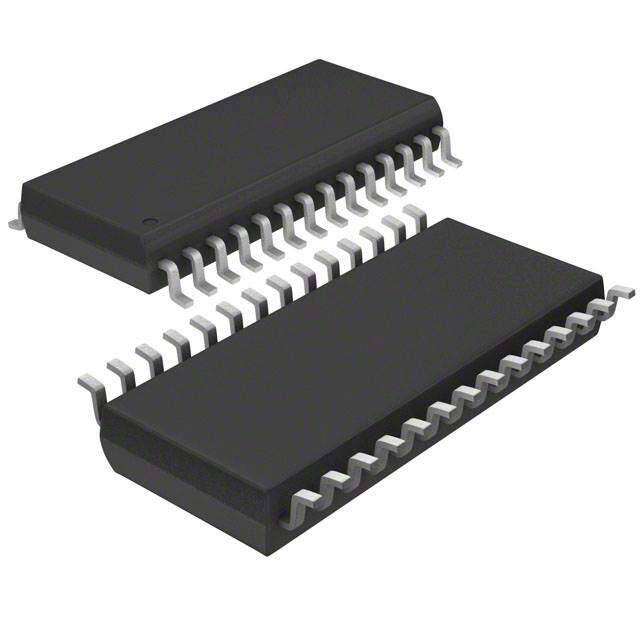
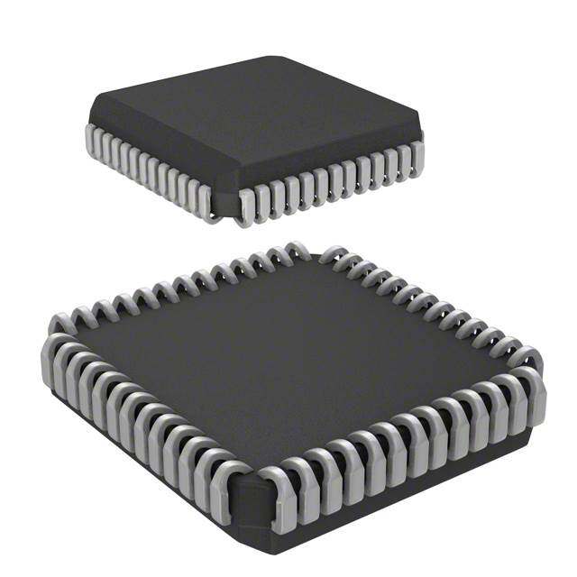
| 供应商器件封装 | 20-SOIC |
| 其它名称 | 296-13457-5 |
| 制造商产品页 | http://www.ti.com/general/docs/suppproductinfo.tsp?distId=10&orderablePartNumber=MSP430F1121AIDW |
| 包装 | 管件 |
| 单位重量 | 500.700 mg |
| 可编程输入/输出端数量 | 14 |
| 商标 | Texas Instruments |
| 商标名 | MSP430 |
| 处理器系列 | 1 Series |
| 外设 | POR,WDT |
| 安装风格 | SMD/SMT |
| 定时器数量 | 1 Timer |
| 封装 | Tube |
| 封装/外壳 | 20-SOIC(0.295",7.50mm 宽) |
| 封装/箱体 | SOIC-20 Wide |
| 工作温度 | -40°C ~ 85°C |
| 工作电源电压 | 1.8 V to 3.6 V |
| 工厂包装数量 | 25 |
| 振荡器类型 | 内部 |
| 接口类型 | Timer UART |
| 数据RAM大小 | 256 B |
| 数据ROM大小 | 256 B |
| 数据Rom类型 | Flash |
| 数据总线宽度 | 16 bit |
| 数据转换器 | 斜率 A/D |
| 最大工作温度 | + 85 C |
| 最大时钟频率 | 8 MHz |
| 最小工作温度 | - 40 C |
| 标准包装 | 25 |
| 核心 | MSP430 |
| 核心处理器 | MSP430 |
| 核心尺寸 | 16-位 |
| 片上ADC | Yes |
| 电压-电源(Vcc/Vdd) | 1.8 V ~ 3.6 V |
| 程序存储器大小 | 4 kB |
| 程序存储器类型 | 闪存 |
| 程序存储容量 | 4KB(4K x 8 + 256B) |
| 系列 | MSP430F1121A |
| 输入/输出端数量 | 14 I/O |
| 连接性 | - |
| 速度 | 8MHz |
| 配用 | /product-detail/zh/MSP-FET430U28/296-22910-ND/1571926/product-detail/zh/MSP-TS430PM64/296-24191-ND/2021636 |


- 商务部:美国ITC正式对集成电路等产品启动337调查
- 曝三星4nm工艺存在良率问题 高通将骁龙8 Gen1或转产台积电
- 太阳诱电将投资9.5亿元在常州建新厂生产MLCC 预计2023年完工
- 英特尔发布欧洲新工厂建设计划 深化IDM 2.0 战略
- 台积电先进制程称霸业界 有大客户加持明年业绩稳了
- 达到5530亿美元!SIA预计今年全球半导体销售额将创下新高
- 英特尔拟将自动驾驶子公司Mobileye上市 估值或超500亿美元
- 三星加码芯片和SET,合并消费电子和移动部门,撤换高东真等 CEO
- 三星电子宣布重大人事变动 还合并消费电子和移动部门
- 海关总署:前11个月进口集成电路产品价值2.52万亿元 增长14.8%


PDF Datasheet 数据手册内容提取
MSP430C11x1, MSP430F11x1A MIXED SIGNAL MICROCONTROLLER SLAS241I − SEPTEMBER 1999 − REVISED DECEMBER 2008 (cid:2) (cid:2) Low Supply Voltage Range 1.8 V to 3.6 V Serial Onboard Programming, (cid:2) Ultralow Power Consumption No External Programming Voltage Needed, − Active Mode: 160 μA at 1 MHz, 2.2 V Programmable Code Protection by − Standby Mode: 0.7 μA Security Fuse − Off Mode (RAM Retention): 0.1 μA (cid:2) Family Members Include (cid:2) Wake-Up From Standby Mode in MSP430C1101: 1KB ROM, 128B RAM Less Than 6 μs MSP430C1111: 2KB ROM, 128B RAM (cid:2) MSP430C1121: 4KB ROM, 256B RAM 16-Bit RISC Architecture, 125 ns MSP430F1101A: 1KB + 128B Flash Memory Instruction Cycle Time 128B RAM (cid:2) Basic Clock Module Configurations: MSP430F1111A: 2KB + 256B Flash Memory − Various Internal Resistors 128B RAM − Single External Resistor MSP430F1121A: 4KB + 256B Flash Memory − 32-kHz Crystal 256B RAM − High-Frequency Crystal (cid:2) Available in a 20-Pin Plastic Small-Outline − Resonator Wide Body (SOWB) Package, 20-Pin Plastic − External Clock Source Small-Outline Thin Package, 20-Pin TVSOP (cid:2) 16-Bit Timer_A With Three (F11x1A only), and 24-Pin QFN (cid:2) Capture/Compare Registers For Complete Module Descriptions, Refer (cid:2) On-Chip Comparator for Analog Signal to the MSP430x1xx Family User’s Guide, Compare Function or Slope Literature Number SLAU049 Analog-to-Digital (A/D) Conversion description The Texas Instruments MSP430 family of ultralow-power microcontrollers consists of several devices featuring different sets of peripherals targeted for various applications. The architecture, combined with five low-power modes is optimized to achieve extended battery life in portable measurement applications. The device features a powerful 16-bit RISC CPU, 16-bit registers, and constant generators that contribute to maximum code efficiency. The digitally controlled oscillator (DCO) allows wake-up from low-power modes to active mode in less than 6 μs. The MSP430x11x1(A) series is an ultralow-power mixed signal microcontroller with a built-in 16-bit timer, versatile analog comparator and fourteen I/O pins. Typical applications include sensor systems that capture analog signals, convert them to digital values, and then process the data for display or for transmission to a host system. Stand alone radio frequency (RF) sensor front end is another area of application. The I/O port inputs provide single slope A/D conversion capability on resistive sensors. This integrated circuit can be damaged by ESD. Texas Instruments recommends that all integrated circuits be handled with appropriate precautions. Failure to observe proper handling and installation procedures can cause damage. ESD damage can range from subtle performance degradation to complete device failure. Precision integrated circuits may be more susceptible to damage because very small parametric changes could cause the device not to meet its published specifications. These devices have limited built-in ESD protection. Please be aware that an important notice concerning availability, standard warranty, and use in critical applications of TexasInstruments semiconductor products and disclaimers thereto appears at the end of this data sheet. PRODUCTION DATA information is current as of publication date. Copyright © 2008 Texas Instruments Incorporated Products conform to specifications per the terms of Texas Instruments standard warranty. Production processing does not necessarily include testing of all parameters. POST OFFICE BOX 655303 • DALLAS, TEXAS 75265 1
MSP430C11x1, MSP430F11x1A MIXED SIGNAL MICROCONTROLLER SLAS241I − SEPTEMBER 1999 − REVISED DECEMBER 2008 AVAILABLE OPTIONS PACKAGED DEVICES PLASTIC PLASTIC PLASTIC PLASTIC TA 20-PIN SOWB 20-PIN TSSOP 20-PIN TVSOP 24-PIN QFN (DW) (PW) (DGV) (RGE) MSP430C1101IDW MSP430C1101IPW MSP430C1101IRGE MSP430C1111IDW MSP430C1111IPW MSP430F1101AIDGV MSP430C1111IRGE MMSSPP443300CC11112211IIDDWW MMSSPP443300CC11112211IIPPWW MMSSPP443300FF11111111AAIIDDGGVV MMSSPP443300CC11112211IIRRGGEE −4400°°CC ttoo 8855°°CC MSP430F1101AIDW MSP430F1101AIPW MSP430F1121AIDGV MSP430F1101AIRGE MSP430F1111AIDW MSP430F1111AIPW MSP430F1111AIRGE MSP430F1121AIDW MSP430F1121AIPW MSP430F1121AIRGE 2 POST OFFICE BOX 655303 • DALLAS, TEXAS 75265
MSP430C11x1, MSP430F11x1A MIXED SIGNAL MICROCONTROLLER SLAS241I − SEPTEMBER 1999 − REVISED DECEMBER 2008 DW, PW, or DGV PACKAGE RGE PACKAGE (TOP VIEW) (TOP VIEW) TEST 1 20 P1.7/TA2/TDO/TDI DILK P2.5/RVoCsCc 23 1198 PP11..65//TTAA10//TTDMIS/TCLK DO/TDI/TC VSS 4 17 P1.4/SMCLK/TCK C TT XOUT 5 16 P1.3/TA2 S 2/1/ O AA XIN 6 15 P1.2/TA1 R TT RST/NMI 7 14 P1.1/TA0 2.5/ CCEST1.7/1.6/C P2.0/ACLK 8 13 P1.0/TACLK PVTPPN P2.1/INCLK 9 12 P2.4/CA1/TA2 P2.2/CAOUT/TA0 10 11 P2.3/CA0/TA1 NC 1 2322 2120 18 P1.5/TA0/TMS VSS 2 17 P1.4/SMCLK/TCK XOUT 3 16 P1.3/TA2 XIN 4 15 P1.2/TA1 RST/NMI 5 14 P1.1/TA0 P2.0/ACLK 6 13 P1.0/TACLK 8 9 10 11 K0C12C LANAAN CT TT NT/ 0/1/ 1/IOU CACA 2.A 3/4/ PC 2.2. 2/ PP 2. P Note: NC pins not internally connected Power Pad connection to VSS recommended functional block diagram XIN XOUT VCC VSS RST/NMI P1/JTAG P2 8 6 ROSC Oscillator ACLK Flash/ROM RAM POR I/O Port 1 I/O Port 2 4KB 256B 8 I/Os, with 6 I/Os, with System SMCLK Interrupt Interrupt Clock 2KB 128B Capability Capability 1KB 128B MCLK MAB, Test 4 Bit JTAG MAB,M 1A6B B, it16-Bit Incl.C 1P6U Reg. EmulationModuleversions only) MDBM, D1B6 ,B 1it6-Bit CBouMnsCvB MDB, 8 Bit F ( TEST Watchdog Timer_A3 Comparator Timer A 3 CC Reg 15/16-Bit POST OFFICE BOX 655303 • DALLAS, TEXAS 75265 3
MSP430C11x1, MSP430F11x1A MIXED SIGNAL MICROCONTROLLER SLAS241I − SEPTEMBER 1999 − REVISED DECEMBER 2008 Terminal Functions TERMINAL NO. DDEESSCCRRIIPPTTIIOONN NAME DW, PW, RGE I/O OR DGV P1.0/TACLK 13 13 I/O General-purpose digital I/O pin/Timer_A, clock signal TACLK input P1.1/TA0 14 14 I/O General-purpose digital I/O pin/Timer_A, capture: CCI0A input, compare: Out0 output/BSL transmit P1.2/TA1 15 15 I/O General-purpose digital I/O pin/Timer_A, capture: CCI1A input, compare: Out1 output P1.3/TA2 16 16 I/O General-purpose digital I/O pin/Timer_A, capture: CCI2A input, compare: Out2 output P1.4/SMCLK/TCK 17 17 I/O General-purpose digital I/O pin/SMCLK signal output/test clock, input terminal for device programming and test P1.5/TA0/TMS 18 18 I/O General-purpose digital I/O pin/Timer_A, compare: Out0 output/test mode select, input terminal for device programming and test P1.6/TA1/TDI/TCLK 19 20 I/O General-purpose digital I/O pin/Timer_A, compare: Out1 output/test data input or test clock input P1.7/TA2/TDO/TDI† 20 21 I/O General-purpose digital I/O pin/Timer_A, compare: Out2 output/test data output terminal or data input during programming P2.0/ACLK 8 6 I/O General-purpose digital I/O pin/ACLK output P2.1/INCLK 9 7 I/O General-purpose digital I/O pin/Timer_A, clock signal at INCLK P2.2/CAOUT/TA0 10 8 I/O General-purpose digital I/O pin/Timer_A, capture: CCI0B input/ comparator_A, output/BSL receive P2.3/CA0/TA1 11 10 I/O General-purpose digital I/O pin/Timer_A, compare: Out1 output/ comparator_A, input P2.4/CA1/TA2 12 11 I/O General-purpose digital I/O pin/Timer_A, compare: Out2 output/ comparator_A, input P2.5/ROSC 3 24 I/O General-purpose digital I/O pin/input for external resistor that defines the DCO nominal frequency RST/NMI 7 5 I Reset or nonmaskable interrupt input TEST 1 22 I Selects test mode for JTAG pins on Port1. The device protection fuse is connected to TEST. VCC 2 23 Supply voltage VSS 4 2 Ground reference XIN 6 4 I Input terminal of crystal oscillator XOUT 5 3 O Output terminal of crystal oscillator QFN Pad NA Package NA QFN package pad connection to VSS recommended. Pad †TDO or TDI is selected via JTAG instruction. 4 POST OFFICE BOX 655303 • DALLAS, TEXAS 75265
MSP430C11x1, MSP430F11x1A MIXED SIGNAL MICROCONTROLLER SLAS241I − SEPTEMBER 1999 − REVISED DECEMBER 2008 short-form description CPU The MSP430 CPU has a 16-bit RISC architecture Program Counter PC/R0 that is highly transparent to the application. All operations, other than program-flow instructions, Stack Pointer SP/R1 are performed as register operations in Status Register SR/CG1/R2 conjunction with seven addressing modes for source operand and four addressing modes for Constant Generator CG2/R3 destination operand. General-Purpose Register R4 The CPU is integrated with 16 registers that provide reduced instruction execution time. The General-Purpose Register R5 register-to-register operation execution time is one cycle of the CPU clock. General-Purpose Register R6 Four of the registers, R0 to R3, are dedicated as General-Purpose Register R7 program counter, stack pointer, status register, and constant generator, respectively. The General-Purpose Register R8 remaining registers are general-purpose registers. General-Purpose Register R9 Peripherals are connected to the CPU using data, General-Purpose Register R10 address, and control buses, and can be handled with all instructions. General-Purpose Register R11 instruction set General-Purpose Register R12 The instruction set consists of 51 instructions with three formats and seven address modes. Each General-Purpose Register R13 instruction can operate on word and byte data. Table1 shows examples of the three types of General-Purpose Register R14 instruction formats; Table 2 shows the address General-Purpose Register R15 modes. Table 1. Instruction Word Formats Dual operands, source-destination e.g., ADD R4,R5 R4 + R5 −−−> R5 Single operands, destination only e.g., CALL R8 PC −−>(TOS), R8−−> PC Relative jump, un/conditional e.g., JNE Jump-on-equal bit = 0 Table 2. Address Mode Descriptions ADDRESS MODE S D SYNTAX EXAMPLE OPERATION Register (cid:3) (cid:3) MOV Rs,Rd MOV R10,R11 R10 −−> R11 Indexed (cid:3) (cid:3) MOV X(Rn),Y(Rm) MOV 2(R5),6(R6) M(2+R5)−−> M(6+R6) Symbolic (PC relative) (cid:3) (cid:3) MOV EDE,TONI M(EDE) −−> M(TONI) Absolute (cid:3) (cid:3) MOV &MEM,&TCDAT M(MEM) −−> M(TCDAT) Indirect (cid:3) MOV @Rn,Y(Rm) MOV @R10,Tab(R6) M(R10) −−> M(Tab+R6) Indirect M(R10) −−> R11 (cid:3) MOV @Rn+,Rm MOV @R10+,R11 autoincrement R10 + 2−−> R10 Immediate (cid:3) MOV #X,TONI MOV #45,TONI #45 −−> M(TONI) NOTE: S = source D = destination POST OFFICE BOX 655303 • DALLAS, TEXAS 75265 5
MSP430C11x1, MSP430F11x1A MIXED SIGNAL MICROCONTROLLER SLAS241I − SEPTEMBER 1999 − REVISED DECEMBER 2008 operating modes The MSP430 has one active mode and five software selectable low-power modes of operation. An interrupt event can wake up the device from any of the five low-power modes, service the request, and restore back to the low-power mode on return from the interrupt program. The following six operating modes can be configured by software: (cid:2) Active mode (AM) − All clocks are active. (cid:2) Low-power mode 0 (LPM0) − CPU is disabled. − ACLK and SMCLK remain active. MCLK is disabled. (cid:2) Low-power mode 1 (LPM1) − CPU is disabled. − ACLK and SMCLK remain active. MCLK is disabled. − DCO’s dc generator is disabled if DCO not used in active mode. (cid:2) Low-power mode 2 (LPM2) − CPU is disabled. − MCLK and SMCLK are disabled. − DCO’s dc generator remains enabled. − ACLK remains active. (cid:2) Low-power mode 3 (LPM3) − CPU is disabled. − MCLK and SMCLK are disabled. − DCO’s dc generator is disabled. − ACLK remains active. (cid:2) Low-power mode 4 (LPM4) − CPU is disabled. − ACLK is disabled. − MCLK and SMCLK are disabled. − DCO’s dc generator is disabled. − Crystal oscillator is stopped. 6 POST OFFICE BOX 655303 • DALLAS, TEXAS 75265
MSP430C11x1, MSP430F11x1A MIXED SIGNAL MICROCONTROLLER SLAS241I − SEPTEMBER 1999 − REVISED DECEMBER 2008 interrupt vector addresses The interrupt vectors and the power-up starting address are located in the address range of 0FFFFh to 0FFE0h. The vector contains the 16-bit address of the appropriate interrupt handler instruction sequence. INTERRUPT SOURCE INTERRUPT FLAG SYSTEM INTERRUPT WORD ADDRESS PRIORITY Power-up WDTIFG External reset KEYV Reset 0FFFEh 15, highest Watchdog (see Note 1) Flash Memory NMIIFG NMI (non)-maskable, OFIFG Oscillator fault (non)-maskable, 0FFFCh 14 ACCVIFG Flash memory access violation (non)-maskable (see Notes 1 and 4) 0FFFAh 13 0FFF8h 12 Comparator_A CAIFG maskable 0FFF6h 11 Watchdog Timer WDTIFG maskable 0FFF4h 10 Timer_A3 TACCR0 CCIFG (see Note 2) maskable 0FFF2h 9 TACCR1 CCIFG. Timer_A3 TACCR2 CCIFG maskable 0FFF0h 8 TAIFG (see Notes 1 and 2) 0FFEEh 7 0FFECh 6 0FFEAh 5 0FFE8h 4 I/O Port P2 P2IFG.0 to P2IFG.7 maskable 0FFE6h 3 (eight flags; see Note 3) (see Notes 1 and 2) I/O Port P1 P1IFG.0 to P1IFG.7 maskable 0FFE4h 2 (eight flags) (see Notes 1 and 2) 0FFE2h 1 0FFE0h 0, lowest NOTES: 1. Multiple source flags 2. Interrupt flags are located in the module 3. There are eight Port P2 interrupt flags, but only six Port P2 I/O pins (P2.0−5) implemented on the ’C11x1 and ’F11x1A devices. 4. (non)-maskable: the individual interrupt-enable bit can disable an interrupt event, but the general interrupt enable cannot. Nonmaskable: neither the individual nor the general interrupt-enable bit will disable an interrupt event. POST OFFICE BOX 655303 • DALLAS, TEXAS 75265 7
MSP430C11x1, MSP430F11x1A MIXED SIGNAL MICROCONTROLLER SLAS241I − SEPTEMBER 1999 − REVISED DECEMBER 2008 special function registers Most interrupt and module enable bits are collected into the lowest address space. Special function register bits not allocated to a functional purpose are not physically present in the device. Simple software access is provided with this arrangement. interrupt enable 1 and 2 Address 7 6 5 4 3 2 1 0 0h ACCVIE NMIIE OFIE WDTIE rw-0 rw-0 rw-0 rw-0 WDTIE: Watchdog timer interrupt enable. Inactive if watchdog mode is selected. Active if watchdog timer is configured in interval timer mode. OFIE: Oscillator fault enable NMIIE: (Non)maskable interrupt enable ACCVIE: Flash access violation interrupt enable Address 7 6 5 4 3 2 1 0 01h interrupt flag register 1 and 2 Address 7 6 5 4 3 2 1 0 02h NMIIFG OFIFG WDTIFG rw-0 rw-1 rw-(0) WDTIFG: Set on watchdog timer overflow (in watchdog mode) or security key violation. Reset on V power up or a reset condition at RST/NMI pin in reset mode. CC OFIFG: Flag set on oscillator fault NMIIFG: Set via RST/NMI pin Address 7 6 5 4 3 2 1 0 03h Legend rw: Bit can be read and written. rw-0,1: Bit can be read and written. It is Reset or Set by PUC. rw-(0,1): Bit can be read and written. It is Reset or Set by POR. SFR bit is not present in device 8 POST OFFICE BOX 655303 • DALLAS, TEXAS 75265
MSP430C11x1, MSP430F11x1A MIXED SIGNAL MICROCONTROLLER SLAS241I − SEPTEMBER 1999 − REVISED DECEMBER 2008 memory organization MSP430C1101 MSP430C1111 MSP430C1121 Memory Size 1KB ROM 2KB ROM 4KB ROM Main: interrupt vector ROM 0FFFFh−0FFE0h 0FFFFh−0FFE0h 0FFFFh−0FFE0h Main: code memory ROM 0FFFFh−0FC00h 0FFFFh−0F800h 0FFFFh−0F000h Information memory Size Not applicable Not applicable Not applicable Flash Boot memory Size Not applicable Not applicable Not applicable ROM RAM Size 128 Byte 128 Byte 256 Byte 027Fh − 0200h 027Fh − 0200h 02FFh − 0200h Peripherals 16-bit 01FFh − 0100h 01FFh − 0100h 01FFh − 0100h 8-bit 0FFh − 010h 0FFh − 010h 0FFh − 010h 8-bit SFR 0Fh − 00h 0Fh − 00h 0Fh − 00h MSP430F1101A MSP430F1111A MSP430F1121A Memory Size 1KB Flash 2KB Flash 4KB Flash Main: interrupt vector Flash 0FFFFh−0FFE0h 0FFFFh−0FFE0h 0FFFFh−0FFE0h Main: code memory Flash 0FFFFh−0FC00h 0FFFFh−0F800h 0FFFFh−0F000h Information memory Size 128 Byte 256 Byte 256 Byte Flash 010FFh − 01080h 010FFh − 01000h 010FFh − 01000h Boot memory Size 1KB 1KB 1KB ROM 0FFFh − 0C00h 0FFFh − 0C00h 0FFFh − 0C00h RAM Size 128 Byte 128 Byte 256 Byte 027Fh − 0200h 027Fh − 0200h 02FFh − 0200h Peripherals 16-bit 01FFh − 0100h 01FFh − 0100h 01FFh − 0100h 8-bit 0FFh − 010h 0FFh − 010h 0FFh − 010h 8-bit SFR 0Fh − 00h 0Fh − 00h 0Fh − 00h bootstrap loader (BSL) The MSP430 BSL enables users to program the flash memory or RAM using a UART serial interface. Access to the MSP430 memory via the BSL is protected by user-defined password. For complete description of the features of the BSL and its implementation, see the Application report Features of the MSP430 Bootstrap Loader, Literature Number SLAA089. BSL FUNCTION DW, PW, AND DGV PACKAGE PINS RGE PACKAGE PINS Data Transmit 14 - P1.1 14 - P1.1 Data Receive 10 - P2.2 8 - P2.2 POST OFFICE BOX 655303 • DALLAS, TEXAS 75265 9
MSP430C11x1, MSP430F11x1A MIXED SIGNAL MICROCONTROLLER SLAS241I − SEPTEMBER 1999 − REVISED DECEMBER 2008 flash memory The flash memory can be programmed via the JTAG port, the bootstrap loader, or in-system by the CPU. The CPU can perform single-byte and single-word writes to the flash memory. Features of the flash memory include: (cid:2) Flash memory has n segments of main memory and two segments of information memory (A and B) of 128 bytes each. Each segment in main memory is 512 bytes in size. (cid:2) Segments 0 to n may be erased in one step, or each segment may be individually erased. (cid:2) Segments A and B can be erased individually, or as a group with segments 0 to n. Segments A and B are also called information memory. (cid:2) New devices may have some bytes programmed in the information memory (needed for test during manufacturing). The user should perform an erase of the information memory prior to the first use. 0FFFFh Segment0 w/ 0FE00h Interrupt Vectors 0FDFFh Segment1 0FC00h 0FBFFh Segment2 0FA00h 0F9FFh Segment3 0F800h 0F7FFh Flash Main Memory Segment4 0F600h 0F5FFh Segment5 0F400h 0F3FFh Segment6 0F200h 0F1FFh Segment7 0F000h 010FFh SegmentA 01080h Information Memory 0107Fh SegmentB 01000h NOTE: All segments not implemented on all devices. 10 POST OFFICE BOX 655303 • DALLAS, TEXAS 75265
MSP430C11x1, MSP430F11x1A MIXED SIGNAL MICROCONTROLLER SLAS241I − SEPTEMBER 1999 − REVISED DECEMBER 2008 peripherals Peripherals are connected to the CPU through data, address, and control buses and can be handled using all instructions. For complete module descriptions, see the MSP430x1xx Family User’s Guide, literature number SLAU049. oscillator and system clock The clock system is supported by the basic clock module that includes support for a 32768-Hz watch crystal oscillator, an internal digitally-controlled oscillator (DCO), and a high-frequency crystal oscillator. The basic clock module is designed to meet the requirements of both low system cost and low power consumption. The internal DCO provides a fast turn-on clock source and stabilizes in less than 6 μs. The basic clock module provides the following clock signals: (cid:2) Auxiliary clock (ACLK), sourced from a 32768-Hz watch crystal or a high-frequency crystal (cid:2) Main clock (MCLK), the system clock used by the CPU (cid:2) Sub-Main clock (SMCLK), the subsystem clock used by the peripheral modules digital I/O There are two 8-bit I/O ports implemented—ports P1 and P2 (only six P2 I/O signals are available on external pins): (cid:2) All individual I/O bits are independently programmable. (cid:2) Any combination of input, output, and interrupt conditions is possible. (cid:2) Edge-selectable interrupt input capability for all the eight bits of port P1 and six bits of port P2. (cid:2) Read/write access to port-control registers is supported by all instructions. NOTE: Only six bits of port P2 (P2.0 to P2.5) are available on external pins, but all control and data bits for port P2 are implemented. watchdog timer (WDT) The primary function of the WDT module is to perform a controlled system restart after a software problem occurs. If the selected time interval expires, a system reset is generated. If the watchdog function is not needed in an application, the module can be configured as an interval timer and can generate interrupts at selected time intervals. Comparator_A The primary function of the Comparator_A module is to support precision slope analog-to-digital conversions, battery-voltage supervision, and monitoring of external analog signals. POST OFFICE BOX 655303 • DALLAS, TEXAS 75265 11
MSP430C11x1, MSP430F11x1A MIXED SIGNAL MICROCONTROLLER SLAS241I − SEPTEMBER 1999 − REVISED DECEMBER 2008 Timer_A3 Timer_A3 is a 16-bit timer/counter with three capture/compare registers. Timer_A3 can support multiple capture/compares, PWM outputs, and interval timing. Timer_A3 also has extensive interrupt capabilities. Interrupts may be generated from the counter on overflow conditions and from each of the capture/compare registers. TIMER_A3 SIGNAL CONNECTIONS INPUT PIN NUMBER MODULE OUTPUT PIN NUMBER DDEEVVIICCEE IINNPPUUTT MMOODDUULLEE MMOODDUULLEE OOUUTTPPUUTT SIGNAL INPUT NAME BLOCK DW, PW, DGV RGE SIGNAL DW, PW, DGV RGE 13 - P1.0 13 - P1.0 TACLK TACLK ACLK ACLK TTiimmeerr NNAA SMCLK SMCLK 9 - P2.1 7 - P2.1 INCLK INCLK 14 - P1.1 14 - P1.1 TA0 CCI0A 14 - P1.1 14 - P1.1 10 - P2.2 8 - P2.2 TA0 CCI0B 18 - P1.5 18 - P1.5 CCCCRR00 TTAA00 VSS GND VCC VCC 15 - P1.2 15 - P1.2 TA1 CCI1A 11 - P2.3 10 - P2.3 CAOUT CCI1B 15 - P1.2 15 - P1.2 (internal) CCCCRR11 TTAA11 VSS GND 19 - P1.6 20 - P1.6 VCC VCC 16 - P1.3 16 - P1.3 TA2 CCI2A 12 - P2.4 11 - P2.4 ACLK (internal) CCI2B 16 - P1.3 16 - P1.3 CCCCRR22 TTAA22 VSS GND 20 - P1.7 21 - P1.7 VCC VCC 12 POST OFFICE BOX 655303 • DALLAS, TEXAS 75265
MSP430C11x1, MSP430F11x1A MIXED SIGNAL MICROCONTROLLER SLAS241I − SEPTEMBER 1999 − REVISED DECEMBER 2008 peripheral file map PERIPHERALS WITH WORD ACCESS Timer_A Reserved 017Eh Reserved 017Ch Reserved 017Ah Reserved 0178h Capture/compare register TACCR2 0176h Capture/compare register TACCR1 0174h Capture/compare register TACCR0 0172h Timer_A register TAR 0170h Reserved 016Eh Reserved 016Ch Reserved 016Ah Reserved 0168h Capture/compare control TACCTL2 0166h Capture/compare control TACCTL1 0164h Capture/compare control TACCTL0 0162h Timer_A control TACTL 0160h Timer_A interrupt vector TAIV 012Eh Flash Memory Flash control 3 FCTL3 012Ch Flash control 2 FCTL2 012Ah Flash control 1 FCTL1 0128h Watchdog Watchdog/timer control WDTCTL 0120h PERIPHERALS WITH BYTE ACCESS Comparator_A Comparator_A port disable CAPD 05Bh Comparator_A control 2 CACTL2 05Ah Comparator_A control 1 CACTL1 059h Basic Clock Basic clock system control 2 BCSCTL2 058h Basic clock system control 1 BCSCTL1 057h DCO clock frequency control DCOCTL 056h Port P2 Port P2 selection P2SEL 02Eh Port P2 interrupt enable P2IE 02Dh Port P2 interrupt edge select P2IES 02Ch Port P2 interrupt flag P2IFG 02Bh Port P2 direction P2DIR 02Ah Port P2 output P2OUT 029h Port P2 input P2IN 028h Port P1 Port P1 selection P1SEL 026h Port P1 interrupt enable P1IE 025h Port P1 interrupt edge select P1IES 024h Port P1 interrupt flag P1IFG 023h Port P1 direction P1DIR 022h Port P1 output P1OUT 021h Port P1 input P1IN 020h Special Function SFR interrupt flag 2 IFG2 003h SFR interrupt flag 1 IFG1 002h SFR interrupt enable 2 IE2 001h SFR interrupt enable 1 IE1 000h POST OFFICE BOX 655303 • DALLAS, TEXAS 75265 13
MSP430C11x1, MSP430F11x1A MIXED SIGNAL MICROCONTROLLER SLAS241I − SEPTEMBER 1999 − REVISED DECEMBER 2008 absolute maximum ratings† Voltage applied at V to V . . . . . . . . . . . . . . . . . . . . . . . . . . . . . . . . . . . . . . . . . . . . . . . . . . . . . . −0.3 V to 4.1 V CC SS Voltage applied to any pin (see Note) . . . . . . . . . . . . . . . . . . . . . . . . . . . . . . . . . . . . . . . . . . . −0.3 V to V +0.3 V CC Diode current at any device terminal . . . . . . . . . . . . . . . . . . . . . . . . . . . . . . . . . . . . . . . . . . . . . . . . . . . . . . . . ±2 mA Storage temperature, T (unprogrammed device) . . . . . . . . . . . . . . . . . . . . . . . . . . . . . . . . . . . −55°C to 150°C stg Storage temperature, T (programmed device) . . . . . . . . . . . . . . . . . . . . . . . . . . . . . . . . . . . . . . −40°C to 85°C stg †Stresses beyond those listed under “absolute maximum ratings” may cause permanent damage to the device. These are stress ratings only, and functional operation of the device at these or any other conditions beyond those indicated under “recommended operating conditions” is not implied. Exposure to absolute-maximum-rated conditions for extended periods may affect device reliability. NOTE: All voltages referenced to VSS. The JTAG fuse-blow voltage, VFB, is allowed to exceed the absolute maximum rating. The voltage is applied to the TEST pin when blowing the JTAG fuse. recommended operating conditions MIN NOM MAX UNITS MMSSPP443300CC1111xx11 11.88 33.66 SSuuppppllyy vvoollttaaggee dduurriinngg pprrooggrraamm eexxeeccuuttiioonn, VVCC ((sseeee NNoottee 11)) MSP430F11x1A 1.8 3.6 VV Supply voltage during program/erase flash memory, VCC MSP430F11x1A 2.7 3.6 V Supply voltage, VSS 0 V Operating free-air temperature range, TA MSP430x11x1(A) −40 85 °C LF mode selected, XTS=0 Watch crystal 32768 Hz LLFFXXTT11 crysttall ffrequency, ff(LFXT1) Ceramic resonator 450 8000 ((sseeee NNootteess 11 aanndd 22)) XXTT11 mmooddee sseelleecctteedd, XXTTSS=11 kkHHzz Crystal 1000 8000 VCC = 1.8 V, dc 4.15 MSP430x11x1(A) PPrroocceessssoorr ffrreeqquueennccyy ff(system) ((MMCCLLKK ssiiggnnaall)) MMHHzz VCC = 3.6 V, dc 8 MSP430x11x1(A) NOTES: 1. In LF mode, the LFXT1 oscillator requires a watch crystal. A 5.1MΩ resistor from XOUT to VSS is recommended when VCC <2.5 V. In XT1 mode, the LFXT1 and XT2 oscillators accept a ceramic resonator or crystal up to 4.15MHz at VCC ≥ 2.2 V. In XT1 mode, the LFXT1 and XT2 oscillators accept a ceramic resonator or crystal up to 8 MHz at VCC ≥ 2.8 V. 2. In LF mode, the LFXT1 oscillator requires a watch crystal. In XT1 mode, LFXT1 accepts a ceramic resonator or a crystal. fSYSTEM (MHz) ÎÎÎÎÎ 8.0 MHz Supply voltage ranÎge,ÎÎÎÎ Supply voltage range, ’F11x1A, ’x11x1(A), during ÎÎÎÎÎduring flash memory programming program execution ÎÎÎÎÎ ÎÎÎÎÎ 4.15 MHz ÎÎÎÎÎ ÎÎÎÎÎ ÎÎÎÎÎ ÎÎÎÎÎ 1.8 V 2.7 V 3 V 3.6 V Supply Voltage − V NOTE: Minimum processor frequency is defined by system clock. Flash program or erase operations require a minimum VCC of 2.7 V. Figure 1. Frequency vs Supply Voltage 14 POST OFFICE BOX 655303 • DALLAS, TEXAS 75265
MSP430C11x1, MSP430F11x1A MIXED SIGNAL MICROCONTROLLER SLAS241I − SEPTEMBER 1999 − REVISED DECEMBER 2008 electrical characteristics over recommended ranges of supply voltage and operating free-air temperature (unless otherwise noted) supply current (into V ) excluding external current CC PARAMETER TEST CONDITIONS VCC MIN TYP MAX UNIT TA = −40°C to 85°C, 2.2 V 160 200 ff(MCLK) = ff(SMCLK) = 11 MMHHzz, CC1111xx11 f(ACLK) = 32,768 Hz 3 V 240 300 TTAA == −4400°CC ttoo 8855°CC,, 2.2 V 1.3 2 f(MCLK) = f(SMCLK) = f(ACLK) = 4096 Hz 3 V 2.5 3.2 I(AM) Active mode TA = −40°C to 85°C, 2.2 V 200 250 μA ffMMCCLLKK == ff((SSMMCCLLKK)) == 11 MMHHzz,, f(ACLK) = 32,768 Hz, 3 V 300 350 FF1111xx11AA Program executes in flash TA = −40°C to 85°C, 2.2 V 3 5 PPrrooggrraamm eexxeeccuutteess iinn ffllaasshh f(MCLK) = f(SMCLK) = f(ACLK) = 4096 Hz 3 V 11 18 TA = −40°C to 85°C, 2.2 V 30 40 CC1111xx11 ff(MCLK) = 00, ff(SMCLK) = 11 MMHHzz, II(CPUOff) LL(LooPwwM-pp0oo)wweerr mmooddee fT(AAC =L K−)4 =0 °3C2 ,t7o6 885 H°Cz, 23.2 V V 5312 6405 μμAA FF1111xx11AA ff(MCLK) = 00, ff(SMCLK) = 11 MMHHzz, f(ACLK) = 32,768 Hz 3 V 55 70 TA = −40°C to 85°C, 2.2 V 11 14 II(LPM2) LLooww-ppoowweerr mmooddee ((LLPPMM22)) ff(MCLK) = ff(SMCLK) = 00 MMHHzz, μμAA f(ACLK) = 32,768 Hz, SCG0 = 0 3 V 17 22 TA = −40°C to 85°C, 2.2 V 1.2 1.7 CC1111xx11 ff(MCLK) = ff(SMCLK) = 00 MMHHzz, f(ACLK) = 32,768 Hz, SCG0 = 1 3 V 2 2.7 TA = −40°C 0.8 1.2 LLooww-ppoowweerr mmooddee II((LLPPMM33)) ((LLPPMM33)) FF1111xx11AA TTAA == 2855°°CC ffff((((MMSSMMCCCCLLKKLL))KK ))== == 00 00 MM MMHHHHzz,zz,, 2.2 V 01..76 2.13 μμAA TA = −40°C f((AACCLLKK)) = 32,768 Hz, 1.8 2.2 TA = 25°C SSCCGG00 = 11 3 V 1.6 1.9 TA = 85°C 2.3 3.4 TA = −40°C 0.1 0.5 C11x1 TA = 25°C 2.2 V/3 V 0.1 0.5 LLooww-ppoowweerr mmooddee TA = 85°C f(MCLK) = 0 MHz, 0.4 0.8 II(LPM4) (LPM4) TA = −40°C ffff((((SSAACCMMLLCCKKLL))KK ==)) ==00 00HH zzMM,, HHSSzzCC,GG00 == 11 0.1 0.5 μμAA F11x1A TA = 25°C 2.2 V/3 V 0.1 0.5 TA = 85°C 0.8 1.9 NOTE: All inputs are tied to 0 V or VCC. Outputs do not source or sink any current. current consumption of active mode versus system frequency, C version, F version IAM = IAM[1 MHz] × fsystem [MHz] current consumption of active mode versus supply voltage, C version IAM = IAM[3 V] + 105 μA/V × (VCC−3 V) current consumption of active mode versus supply voltage, F version IAM = IAM[3 V] + 120 μA/V × (VCC−3 V) POST OFFICE BOX 655303 • DALLAS, TEXAS 75265 15
MSP430C11x1, MSP430F11x1A MIXED SIGNAL MICROCONTROLLER SLAS241I − SEPTEMBER 1999 − REVISED DECEMBER 2008 electrical characteristics over recommended ranges of supply voltage and operating free-air temperature (unless otherwise noted) (continued) Schmitt-trigger inputs − Ports P1 (P1.0 to P1.7) and P2 (P2.0 to P2.5) PARAMETER VCC MIN TYP MAX UNIT 2.2 V 1.1 1.5 VVIT+ PPoossiittiivvee-ggooiinngg iinnppuutt tthhrreesshhoolldd vvoollttaaggee 3 V 1.5 1.9 VV 2.2 V 0.4 0.9 VVIT− NNeeggaattiivvee-ggooiinngg iinnppuutt tthhrreesshhoolldd vvoollttaaggee 3 V 0.9 1.3 VV 2.2 V 0.3 1.1 VVhys IInnppuutt vvoollttaaggee hhyysstteerreessiiss ((VVIT+ − VVIT−)) VV 3 V 0.5 1 standard inputs − RST/NMI, JTAG (TCK, TMS, TDI/TCLK) PARAMETER VCC MIN TYP MAX UNIT VIL Low-level input voltage VSS VSS+0.6 V 22.22 VV // 33 VV VIH High-level input voltage 0.8×VCC VCC V inputs Px.x, TAx PARAMETER TEST CONDITIONS VCC MIN TYP MAX UNIT 2.2 V/3 V 1.5 cycle PPortt PP11, PP22: PP11.x tto PP22.x, EExtternall ttriigger siignall t((iinntt)) External interruppt timingg ffoorr tthhee iinntteerrrruupptt ffllaagg ((sseeee NNoottee 11)) 2.2 V 62 nnss 3 V 50 2.2 V 62 tt((cap)) TTiimmeerr_AA, ccaappttuurree ttiimmiinngg TTAA00, TTAA11, TTAA22 nnss 3 V 50 TTiimmeerr__AA cclloocckk ffrreeqquueennccyy 2.2 V 8 ff(TAext) externally applied to pin TTAACCLLKK, IINNCCLLKK tt(H) == tt(L) 3 V 10 MMHHzz 2.2 V 8 ff(TAint) TTiimmeerr_AA cclloocckk ffrreeqquueennccyy SSMMCCLLKK oorr AACCLLKK ssiiggnnaall sseelleecctteedd MMHHzz 3 V 10 NOTES: 1. The external signal sets the interrupt flag every time the minimum t(int) cycle and time parameters are met. It may be set even with trigger signals shorter than t(int). Both the cycle and timing specifications must be met to ensure the flag is set. t(int) is measured in MCLK cycles. leakage current PARAMETER TEST CONDITIONS VCC MIN TYP MAX UNIT Port P1: P1.x, 0 ≤ ×≤ 7 2.2 V/3 V ±50 (see Notes 1 and 2) IIlkg(Px.x) HHiigghh-iimmppeeddaannccee lleeaakkaaggee ccuurrrreenntt Port P2: P2.x, 0 ≤ ×≤ 5 nnAA 2.2 V/3 V ±50 (see Notes 1 and 2) NOTES: 1. The leakage current is measured with VSS or VCC applied to the corresponding pin(s), unless otherwise noted. 2. The leakage of the digital port pins is measured individually. The port pin must be selected for input and there must be no optional pullup or pulldown resistor. 16 POST OFFICE BOX 655303 • DALLAS, TEXAS 75265
MSP430C11x1, MSP430F11x1A MIXED SIGNAL MICROCONTROLLER SLAS241I − SEPTEMBER 1999 − REVISED DECEMBER 2008 electrical characteristics over recommended ranges of supply voltage and operating free-air temperature (unless otherwise noted) (continued) outputs − Ports P1 (P1.0 to P1.7) and P2 (P2.0 to P2.5) PARAMETER TEST CONDITIONS MIN TYP MAX UNIT I(OHmax) = −1.5 mA See Note 1 VCC−0.25 VCC High-level output voltage I(OHmax) = −6 mA VVCC = 22.22 VV See Note 2 VCC−0.6 VCC VVOH PPPPoooorrrrtttt 1111 ((aaFFnn11dd11 PPxx11ooAArrtt)) 22 ((CC1111xx11)) I(OHmax) = −1.5 mA See Note 1 VCC−0.25 VCC VV I(OHmax) = −6 mA VVCC = 33 VV See Note 2 VCC−0.6 VCC I(OHmax) = −1 mA See Note 3 VCC−0.25 VCC HHiigghh-lleevveell oouuttppuutt vvoollttaaggee I(OHmax) = −3.4 mA VVCC = 22.22 VV See Note 3 VCC−0.6 VCC VVOH Port 2 (F11x1A) I(OHmax) = −1 mA See Note 3 VCC−0.25 VCC VV I(OHmax) = −3.4 mA VVCC = 33 VV See Note 3 VCC−0.6 VCC I(OLmax) = 1.5 mA See Note 1 VSS VSS+0.25 Low-level output voltage I(OLmax) = 6 mA VVCC = 22.22 VV See Note 2 VSS VSS+0.6 VVOL PPFF11oo11rrttxx 1111 AAaa))nndd PPoorrtt 22 ((CC1111xx11, I(OLmax) = 1.5 mA See Note 1 VSS VSS+0.25 VV VVCC == 33 VV I(OLmax) = 6 mA See Note 2 VSS VSS+0.6 NOTES: 1. The maximum total current, IOHmax and IOLmax, for all outputs combined, should not exceed ±12 mA to hold the maximum voltage drop specified. 2. The maximum total current, IOHmax and IOLmax, for all outputs combined, should not exceed ±48 mA to hold the maximum voltage drop specified. 3. One output loaded at a time. output frequency PARAMETER TEST CONDITIONS VCC MIN TYP MAX UNIT fP20 P2.0/ACLK, CL = 20 pF 2.2 V/3 V fSystem fTAx Output frequency TInAte0r,n TaAl 1c,lo TcAk2 s,o CuLrc =e ,2 S0 MpFCLK signal applied (see Note 1) 2.2 V/3 V dc fSystem MHz fSMCLK = fLFXT1 = fXT1 40% 60% fSMCLK = fLFXT1 = fLF 35% 65% PP11.44//SSMMCCLLKK, 22.22 VV//33 VV 50%− 50%+ CL = 20 pF fSMCLK = fLFXT1/n 15 ns 50% 15 ns tXdc Dffrreeuqqtyuu eecynnccclyye of O/P fSMCLK = fDCOCLK 2.2 V/3 V 5105% n−s 50% 5105% n+s fP20 = fLFXT1 = fXT1 40% 60% PP22.00//AACCLLKK, CCLL == 2200 ppFF fP20 = fLFXT1 = fLF 2.2 V/3 V 30% 70% fP20 = fLFXT1/n 50% tTAdc TA0, TA1, TA2, CL = 20 pF, duty cycle = 50% 2.2 V/3 V 0 ±50 ns NOTE 1: The limits of the system clock MCLK has to be met. MCLK and SMCLK can have different frequencies. POST OFFICE BOX 655303 • DALLAS, TEXAS 75265 17
MSP430C11x1, MSP430F11x1A MIXED SIGNAL MICROCONTROLLER SLAS241I − SEPTEMBER 1999 − REVISED DECEMBER 2008 electrical characteristics over recommended ranges of supply voltage and operating free-air temperature (unless otherwise noted) (continued) outputs − Ports P1 and P2 (continued) TYPICAL LOW-LEVEL OUTPUT CURRENT TYPICAL LOW-LEVEL OUTPUT CURRENT vs vs LOW-LEVEL OUTPUT VOLTAGE LOW-LEVEL OUTPUT VOLTAGE 16 25 mA VCC = 2.2 V TA = 25°C mA VCC = 3 V − 14 P1.0 − P1.0 TA = 25°C Current 12 TA = 85°C Current 20 TA = 85°C ut ut p 10 p ut ut 15 O O el 8 el v v e e L L w- 6 w- 10 o o L L al al pic 4 pic Ty Ty 5 − 2 − L L O O I I 0 0 0.0 0.5 1.0 1.5 2.0 2.5 0.0 0.5 1.0 1.5 2.0 2.5 3.0 3.5 VOL − Low-Level Output Voltage − V VOL − Low-Level Output Voltage − V Figure 2 Figure 3 TYPICAL HIGH-LEVEL OUTPUT CURRENT TYPICAL HIGH-LEVEL OUTPUT CURRENT vs vs HIGH-LEVEL OUTPUT VOLTAGE HIGH-LEVEL OUTPUT VOLTAGE 0 0 ent − mA −2 VPC1.C0 = 2.2 V nt − mA −5 VPC1.C0 = 3 V Curr −4 urre put ut C −10 Out −6 utp vel el O −15 e v L −8 e gh- h-L ypical Hi −10 TA = 85°C pical Hig −20 TA = 85°C T y − OH −12 − TH −25 TA = 25°C I TA = 25°C O −14 I −30 0.0 0.5 1.0 1.5 2.0 2.5 0.0 0.5 1.0 1.5 2.0 2.5 3.0 3.5 VOH − High-Level Output Voltage − V VOH − High-Level Output Voltage − V Figure 4 Figure 5 NOTE: One output loaded at a time. 18 POST OFFICE BOX 655303 • DALLAS, TEXAS 75265
MSP430C11x1, MSP430F11x1A MIXED SIGNAL MICROCONTROLLER SLAS241I − SEPTEMBER 1999 − REVISED DECEMBER 2008 electrical characteristics over recommended ranges of supply voltage and operating free-air temperature (unless otherwise noted) (continued) optional resistors, individually programmable with ROM code (see Note 1) PARAMETER TEST CONDITIONS MIN TYP MAX UNIT R(opt1) 2.5 5 10 kΩ R(opt2) 3.8 7.7 15 kΩ R(opt3) 7.6 15 31 kΩ R(opt4) 11.5 23 46 kΩ R(opt5) RReessiissttoorrss,, iinnddiivviidduuaallllyy pprrooggrraammmmaabbllee wwiitthh RROOMM ccooddee,, aallll ppoorrtt ppiinnss,, 23 45 90 kΩ R(opt6) values applicable for pulldown and pullup VVCC = 22.22 VV//33 VV 46 90 180 kΩ R(opt7) 70 140 280 kΩ R(opt8) 115 230 460 kΩ R(opt9) 160 320 640 kΩ R(opt10) 205 420 830 kΩ NOTE 1: Optional resistors Roptx for pulldown or pullup are not available in standard flash memory device MSP430F11x1A. wake-up from low-power modes (LPMx) PARAMETER TEST CONDITIONS MIN TYP MAX UNIT t(LPM0) VCC = 2.2 V/3 V 100 nnss t(LPM2) VCC = 2.2 V/3 V 100 f(MCLK) = 1 MHz, VCC = 2.2 V/3 V 6 t((LLPPMM33)) f(MCLK) = 2 MHz, VCC = 2.2 V/3 V 6 μμs DDeellaayy ttiimmee ((sseeee NNoottee 11)) f(MCLK) = 3 MHz, VCC = 2.2 V/3 V 6 f(MCLK) = 1 MHz, VCC = 2.2 V/3 V 6 t((LLPPMM44)) f(MCLK) = 2 MHz, VCC = 2.2 V/3 V 6 μμs f(MCLK) = 3 MHz, VCC = 2.2 V/3 V 6 NOTE 1: Parameter applicable only if DCOCLK is used for MCLK. RAM PARAMETER MIN TYP MAX UNIT V(RAMh) CPU halted (see Note 1) 1.6 V NOTE 1: This parameter defines the minimum supply voltage VCC when the data in the program memory RAM remains unchanged. No program execution should happen during this supply voltage condition. POST OFFICE BOX 655303 • DALLAS, TEXAS 75265 19
MSP430C11x1, MSP430F11x1A MIXED SIGNAL MICROCONTROLLER SLAS241I − SEPTEMBER 1999 − REVISED DECEMBER 2008 electrical characteristics over recommended ranges of supply voltage and operating free-air temperature (unless otherwise noted) (continued) Comparator_A (see Note 1) PARAMETER TEST CONDITIONS MIN TYP MAX UNIT II(DD) CCAAOONN==11, CCAARRSSEELL==00, CCAARREEFF==00 VCC = 2.2 V 25 40 μμAA VCC = 3 V 45 60 CAON=1, CARSEL=0, VCC = 2.2 V 30 50 II(Refladder/RefDiode) CCAARREEFF=11//22//33, nnoo llooaadd aatt μμAA P2.3/CA0/TA1 and P2.4/CA1/TA2 VCC = 3 V 45 71 Common-mode input V(IC) voltage CAON =1 VCC = 2.2 V/3 V 0 VCC−1 V PCA0=1, CARSEL=1, CAREF=1, Voltage@0.25V node V(Ref025) CC No load at P2.3/CA0/TA1 and VCC = 2.2 V/3 V 0.23 0.24 0.25 V CC P2.4/CA1/TA2 Voltage@0.5V node PCA0=1, CARSEL=1, CAREF=2, CC V(Ref050) V No load at P2.3/CA0/TA1 and VCC = 2.2 V/3 V 0.47 0.48 0.5 CC P2.4/CA1/TA2 PCA0=1, CARSEL=1, CAREF=3, VCC = 2.2 V 390 480 540 VV(RefVT) ((sseeee FFiigguurree 66 aanndd FFiigguurree 77)) NNoo llooaadd aatt PP22.33//CCAA00//TTAA11 aanndd mmVV P2.4/CA1/TA2, TA = 85°C VCC = 3 V 400 490 550 V(offset) Offset voltage See Note 2 VCC = 2.2 V/3 V −30 30 mV Vhys Input hysteresis CAON=1 VCC = 2.2 V/3 V 0 0.7 1.4 mV TTAA == 2255°CC,, OOvveerrddrriivvee 1100 mmVV,, VCC = 2.2 V 160 210 300 nnss Without filter: CAF=0 VCC = 3 V 90 150 240 tt(response LH) TTAA == 2255°CC,, OOvveerrddrriivvee 1100 mmVV,, VCC = 2.2 V 1.4 1.9 3.4 μμss With filter: CAF=1 VCC = 3 V 0.9 1.5 2.6 TTAA == 2255°CC,, OOvveerrddrriivvee 1100 mmVV,, VCC = 2.2 V 130 210 300 nnss Without filter: CAF=0 VCC = 3 V 80 150 240 tt(response HL) TTAA == 2255°CC,, OOvveerrddrriivvee 1100 mmVV,, VCC = 2.2 V 1.4 1.9 3.4 μμss With filter: CAF=1 VCC = 3 V 0.9 1.5 2.6 NOTES: 1. The leakage current for the Comparator_A terminals is identical to Ilkg(Px.x) specification. 2. The input offset voltage can be cancelled by using the CAEX bit to invert the Comparator_A inputs on successive measurements. The two successive measurements are then summed together. 20 POST OFFICE BOX 655303 • DALLAS, TEXAS 75265
MSP430C11x1, MSP430F11x1A MIXED SIGNAL MICROCONTROLLER SLAS241I − SEPTEMBER 1999 − REVISED DECEMBER 2008 electrical characteristics over recommended ranges of supply voltage and operating free-air temperature (unless otherwise noted) (continued) 650 650 VCC = 3 V VCC = 2.2 V V 600 V 600 m m − − olts Typical olts Typical V V e 550 e 550 c c n n e e er er ef ef − R 500 − R 500 T) T) V V F F E E V(R 450 V(R 450 400 400 −45 −25 −5 15 35 55 75 95 −45 −25 −5 15 35 55 75 95 TA − Free-Air Temperature − °C TA − Free-Air Temperature − °C Figure 6. V vs Temperature, V = 3 V Figure 7. V vs Temperature, V = 2.2 V (RefVT) CC (RefVT) CC 0 V VCC 0 1 CAF CAON Low Pass Filter To Internal Modules 0 0 V+ + _ V− 1 1 CAOUT Set CAIFG Flag τ ≈ 2.0 μs Figure 8. Block Diagram of Comparator_A Module Overdrive VCAOUT V− 400 mV V+ t(response) Figure 9. Overdrive Definition POST OFFICE BOX 655303 • DALLAS, TEXAS 75265 21
MSP430C11x1, MSP430F11x1A MIXED SIGNAL MICROCONTROLLER SLAS241I − SEPTEMBER 1999 − REVISED DECEMBER 2008 electrical characteristics over recommended ranges of supply voltage and operating free-air temperature (unless otherwise noted) (continued) PUC/POR PARAMETER TEST CONDITIONS MIN TYP MAX UNIT t(POR_Delay) Internal time delay to release POR 150 250 μs VVCCCC tthhrreesshhoolldd aatt wwhhiicchh PPOORR TA = −40°C 1.4 1.8 VVPPOORR rreelleeaassee ddeellaayy ttiimmee bbeeggiinnss TA = 25°C 1.1 1.5 VV (see Note 1) TA = 85°C VCC = 2.2 V/3 V 0.8 1.2 V(min) VgeCnCe trhartees ah oPldO Rre q(sueiree dN otote 2) VCC |dV/dt| ≥ 1V/ms 0.2 V t(reset) RST/NMI low time for PUC/POR Reset is accepted internally 2 μs NOTES: 1. VCC rise time dV/dt ≥ 1V/ms. 2. When driving VCC low in order to generate a POR condition, VCC should be driven to 200mV or lower with a dV/dt equal to or less than −1V/ms. The corresponding rising VCC must also meet the dV/dt requirement equal to or greater than +1V/ms. V VCC V POR No POR POR POR V (min) t Figure 10. Power-On Reset (POR) vs Supply Voltage 2.0 1.8 1.8 1.6 1.5 Max 1.4 V] 1.4 1.2 R [ 1.2 O Min P 1.0 1.1 V 0.8 0.8 0.6 0.4 0.2 25°C 0 −40 −20 0 20 40 60 80 Temperature [°C] Figure 11. V vs Temperature POR 22 POST OFFICE BOX 655303 • DALLAS, TEXAS 75265
MSP430C11x1, MSP430F11x1A MIXED SIGNAL MICROCONTROLLER SLAS241I − SEPTEMBER 1999 − REVISED DECEMBER 2008 electrical characteristics over recommended ranges of supply voltage and operating free-air temperature (unless otherwise noted) (continued) DCO PARAMETER TEST CONDITIONS VCC MIN TYP MAX UNIT 2.2 V 0.08 0.12 0.15 ff(DCO03) RRsel = 00, DDCCOO = 33, MMOODD = 00, DDCCOORR = 00, TTA = 2255°°CC 3 V 0.08 0.13 0.16 MMHHzz 2.2 V 0.14 0.19 0.23 ff(DCO13) RRsel = 11, DDCCOO = 33, MMOODD = 00, DDCCOORR = 00, TTA = 2255°°CC 3 V 0.14 0.18 0.22 MMHHzz 2.2 V 0.22 0.30 0.36 ff((DCCOO23)) RRsel == 22, DDCCOO == 33, MMOODD == 00, DDCCOORR == 00, TTA == 2255°°CC MMHHzz 3 V 0.22 0.28 0.34 2.2 V 0.37 0.49 0.59 ff(DCO33) RRsel == 33, DDCCOO == 33, MMOODD == 00, DDCCOORR == 00, TTA == 2255°°CC MMHHzz 3 V 0.37 0.47 0.56 2.2 V 0.61 0.77 0.93 ff(DCO43) RRsel == 44, DDCCOO == 33, MMOODD == 00, DDCCOORR == 00, TTA == 2255°°CC MMHHzz 3 V 0.61 0.75 0.9 2.2 V 1 1.2 1.5 ff(DCO53) RRsel == 55, DDCCOO == 33, MMOODD == 00, DDCCOORR == 00, TTA == 2255°°CC MMHHzz 3 V 1 1.3 1.5 2.2 V 1.6 1.9 2.2 ff(DCO63) RRsel == 66, DDCCOO == 33, MMOODD == 00, DDCCOORR == 00, TTA == 2255°°CC MMHHzz 3 V 1.69 2 2.29 2.2 V 2.4 2.9 3.4 ff(DCO73) RRsel == 77, DDCCOO == 33, MMOODD == 00, DDCCOORR == 00, TTA == 2255°°CC MMHHzz 3 V 2.7 3.2 3.65 2.2 V 4 4.5 4.9 ff(DCO77) RRsel == 77, DDCCOO == 77, MMOODD == 00, DDCCOORR == 00, TTA == 2255°°CC MMHHzz 3 V 4.4 4.9 5.4 ff(DCO47) RRsel == 44, DDCCOO == 77, MMOODD == 00, DDCCOORR == 00, TTA == 2255°°CC 22.22 VV//33 VV ffDDCCxOO144.700 ffDDCCxOO244.100 ffDDCCxOO244.500 MMHHzz S(Rsel) SR = fRsel+1/fRsel 2.2 V/3 V 1.35 1.65 2 rraattiioo S(DCO) SDCO = fDCO+1/fDCO 2.2 V/3 V 1.07 1.12 1.16 2.2 V −0.31 −0.36 −0.40 DDt TTeemmppeerraattuurree ddrriifftt, RRsel == 44, DDCCOO == 33, MMOODD == 00 ((sseeee NNoottee 11)) %%//°°CC 3 V −0.33 −0.38 −0.43 DV Drift with VCC variation, Rsel = 4, DCO = 3, MOD = 0 (see Note 1) 2.2 V/3 V 0 5 10 %/V NOTE 1: These parameters are not production tested. ÎÎÎÎÎ e Max ÎÎÎÎÎ nc f(DCOx7) aria Min ÎÎÎÎÎ K V L y C uenc ÎÎÎÎÎ 1 DCO q Max f re f(DCOx0) ÎÎÎÎÎ F Min 0 1 2 3 4 5 6 7 2.2 V 3 V VCC DCO Steps Figure 12. DCO Characteristics POST OFFICE BOX 655303 • DALLAS, TEXAS 75265 23
MSP430C11x1, MSP430F11x1A MIXED SIGNAL MICROCONTROLLER SLAS241I − SEPTEMBER 1999 − REVISED DECEMBER 2008 electrical characteristics over recommended ranges of supply voltage and operating free-air temperature (unless otherwise noted) (continued) main DCO characteristics (cid:2) Individual devices have a minimum and maximum operation frequency. The specified parameters for f(DCOx0) to f(DCOx7) are valid for all devices. (cid:2) All ranges selected by Rsel(n) overlap with Rsel(n+1): Rsel0 overlaps Rsel1, ... Rsel6 overlaps Rsel7. (cid:2) DCO control bits DCO0, DCO1, and DCO2 have a step size as defined by parameter S . DCO (cid:2) Modulation control bits MOD0 to MOD4 select how often f(DCO+1) is used within the period of 32 DCOCLK cycles. The frequency f is used for the remaining cycles. The frequency is an average equal to: (DCO) 32(cid:3)f (cid:3)f f (cid:2) (DCO) (DCO(cid:4)1) average MOD(cid:3)f (cid:4)(32(cid:5)MOD)(cid:3)f (DCO) (DCO(cid:4)1) DCO when using ROSC (see Note 1) PARAMETER TEST CONDITIONS VCC MIN TYP MAX UNIT 2.2 V 1.8±15% MHz ffDCCOO, DDCCOO oouuttppuutt ffrreeqquueennccyy RRsel == 44, DDCCOO == 33, MMOODD == 00, DDCCOORR == 11, TTA == 2255°°CC 3 V 1.95±15% MHz Dt, Temperature drift Rsel = 4, DCO = 3, MOD = 0, DCOR = 1 2.2 V/3 V ±0.1 %/°C Dv, Drift with VCC variation Rsel = 4, DCO = 3, MOD = 0, DCOR = 1 2.2 V/3 V 10 %/V NOTES: 1. ROSC = 100kΩ. Metal film resistor, type 0257. 0.6 watt with 1% tolerance and TK = ±50ppm/°C. crystal oscillator, LFXT1 PARAMETER TEST CONDITIONS MIN TYP MAX UNIT XTS=0, LF mode selected, 12 VCC = 2.2 V / 3 V CCXIN IInnppuutt ccaappaacciittaannccee XTS=1, XT1 mode selected, ppFF 2 VCC = 2.2 V / 3 V (see Note 1) XTS=0, LF mode selected, 12 VCC = 2.2 V / 3 V CCXOUT OOuuttppuutt ccaappaacciittaannccee ppFF XTS=1, XT1 mode selected, 2 VCC = 2.2 V / 3 V (see Note 1) VIL VSS 0.2×VCC VIH IInnppuutt lleevveellss aatt XXIINN VVCC == 22.22 VV//33 VV ((sseeee NNoottee 22)) 0.8×VCC VCC VV NOTES: 1. Requires external capacitors at both terminals. Values are specified by crystal manufacturers. 2. Applies only when using an external logic-level clock source. Not applicable when using a crystal or resonator. 24 POST OFFICE BOX 655303 • DALLAS, TEXAS 75265
MSP430C11x1, MSP430F11x1A MIXED SIGNAL MICROCONTROLLER SLAS241I − SEPTEMBER 1999 − REVISED DECEMBER 2008 electrical characteristics over recommended ranges of supply voltage and operating free-air temperature (unless otherwise noted) (continued) flash memory TEST PARAMETER CONDITIONS VCC MIN TYP MAX UNIT VCC(PGM/ Program and erase supply voltage 2.7 3.6 V ERASE) fFTG Flash Timing Generator frequency 257 476 kHz IPGM Supply current from VCC during program 2.7 V/ 3.6 V 3 5 mA IERASE Supply current from VCC during erase 2.7 V/ 3.6 V 3 7 mA tCPT Cumulative program time See Note 1 2.7 V/ 3.6 V 4 ms tCMErase Cumulative mass erase time See Note 2 2.7 V/ 3.6 V 200 ms Program/erase endurance 104 105 cycles tRetention Data retention duration TJ = 25°C 100 years tWord Word or byte program time 35 tBlock, 0 Block program time for first byte or word 30 tBlock, 1-63 Block program time for each additional byte or word 21 tBlock, End Block program end-sequence wait time SSeeee NNoottee 33 6 ttFTG tMass Erase Mass erase time 5297 tSeg Erase Segment erase time 4819 NOTES: 1. The cumulative program time must not be exceeded when writing to a 64-byte flash block. This parameter applies to all programming methods: individual word/byte write and block write modes. 2. The mass erase duration generated by the flash timing generator is at least 11.1ms ( = 5297x1/fFTG,max = 5297x1/476kHz). To achieve the required cumulative mass erase time the Flash Controller’s mass erase operation can be repeated until this time is met. (A worst case minimum of 19 cycles are required). 3. These values are hardwired into the Flash Controller’s state machine (tFTG = 1/fFTG). JTAG interface TEST PARAMETER CONDITIONS VCC MIN TYP MAX UNIT 2.2 V 0 5 MHz ffTCK TTCCKK iinnppuutt ffrreeqquueennccyy sseeee NNoottee 11 3 V 0 10 MHz RInternal Internal pulldown resistance on TEST see Note 2 2.2 V/ 3 V 25 60 90 kΩ NOTES: 1. fTCK may be restricted to meet the timing requirements of the module selected. 2. TEST pull-down resistor implemented in all versions. JTAG fuse (see Note 1) TEST PARAMETER CONDITIONS VCC MIN TYP MAX UNIT VCC(FB) Supply voltage during fuse-blow condition TA = 25°C 2.5 V Voltage level on TEST for fuse blow (’C11x1) 3.5 3.9 V VVFB Voltage level on TEST for fuse blow (’F11x1A) 6 7 V IFB Supply current into TEST during fuse blow 100 mA tFB Time to blow fuse 1 ms NOTES: 1. Once the fuse is blown, no further access to the MSP430 JTAG/Test and emulation (F versions only) features is possible. The JTAG block is switched to bypass mode. POST OFFICE BOX 655303 • DALLAS, TEXAS 75265 25
MSP430C11x1, MSP430F11x1A MIXED SIGNAL MICROCONTROLLER SLAS241I − SEPTEMBER 1999 − REVISED DECEMBER 2008 APPLICATION INFORMATION input/output schematic Port P1, P1.0 to P1.3, input/output with Schmitt trigger VCC P1SEL.x 0 (See Note 1) P1DIR.x Direction Control 1 From Module (See Note 2) P1OUT.x 0 Pad Logic P1.0 − P1.3 1 Module X OUT (See Note 2) (See Note 1) P1IN.x GND EN Module X IN D P1IRQ.x P1IE.x Interrupt EN Q Edge P1IFG.x Set Select Interrupt Flag P1IES.x P1SEL.x NOTE: x = Bit/identifier, 0 to 3 for port P1 Direction PnSel.x PnDIR.x control from PnOUT.x Module X OUT PnIN.x Module X IN PnIE.x PnIFG.x PnIES.x module P1Sel.0 P1DIR.0 P1DIR.0 P1OUT.0 VSS P1IN.0 TACLK† P1IE.0 P1IFG.0 P1IES.0 P1Sel.1 P1DIR.1 P1DIR.1 P1OUT.1 Out0 signal† P1IN.1 CCI0A† P1IE.1 P1IFG.1 P1IES.1 P1Sel.2 P1DIR.2 P1DIR.2 P1OUT.2 Out1 signal† P1IN.2 CCI1A† P1IE.2 P1IFG.2 P1IES.2 P1Sel.3 P1DIR.3 P1DIR.3 P1OUT.3 Out2 signal† P1IN.3 CCI2A† P1IE.3 P1IFG.3 P1IES.3 †Signal from or to Timer_A NOTES: 1. Optional selection of pullup or pulldown resistors with ROM (masked) versions 2. Fuses for optional pullup and pulldown resistors can only be programmed at the factory (ROM versions only). 26 POST OFFICE BOX 655303 • DALLAS, TEXAS 75265
MSP430C11x1, MSP430F11x1A MIXED SIGNAL MICROCONTROLLER SLAS241I − SEPTEMBER 1999 − REVISED DECEMBER 2008 APPLICATION INFORMATION Port P1, P1.4 to P1.7, input/output with Schmitt trigger and in-system access features P1SEL.x VCC 0 P1DIR.x See Note 1 Direction Control 1 From Module See Note 2 00 P1OUT.x Pad Logic 11 P1.4−P1.7 Module X OUT See Note 2 See Note 1 GND TST Bus Keeper P1IN.x EN Module X IN D TEST TST P1IRQ.x P1IE.x EN Interrupt Fuse 60 kΩ Q Edge Typical P1IFG.x Set Select GND Interrupt Fuse Flag P1IES.x Control By JTAG Blow P1SEL.x TSTControl P1.x TDO Controlled By JTAG P1.7/TDI/TDO Controlled by JTAG TDI TST P1.x P1.6/TDI/TCLK NOTE: The test pin should be protected from potential EMI and ESD voltage spikes. This may require a smaller TST P1.x TMS external pulldown resistor in some applications. P1.5/TMS x = Bit identifier, 4 to 7 for port P1 During programming activity and during blowing TST P1.x of the fuse, the pin TDO/TDI is used to apply the test TCK input for JTAG circuitry. P1.4/TCK Direction PnSel.x PnDIR.x control from PnOUT.x Module X OUT PnIN.x Module X IN PnIE.x PnIFG.x PnIES.x module P1Sel.4 P1DIR.4 P1DIR.4 P1OUT.4 SMCLK P1IN.4 unused P1IE.4 P1IFG.4 P1IES.4 P1Sel.5 P1DIR.5 P1DIR.5 P1OUT.5 Out0 signal† P1IN.5 unused P1IE.5 P1IFG.5 P1IES.5 P1Sel.6 P1DIR.6 P1DIR.6 P1OUT.6 Out1 signal† P1IN.6 unused P1IE.6 P1IFG.6 P1IES.6 P1Sel.7 P1DIR.7 P1DIR.7 P1OUT.7 Out2 signal† P1IN.7 unused P1IE.7 P1IFG.7 P1IES.7 †Signal from or to Timer_A NOTES: 1. Optional selection of pullup or pulldown resistors with ROM (masked) versions 2. Fuses for optional pullup and pulldown resistors can only be programmed at the factory (ROM versions only). POST OFFICE BOX 655303 • DALLAS, TEXAS 75265 27
MSP430C11x1, MSP430F11x1A MIXED SIGNAL MICROCONTROLLER SLAS241I − SEPTEMBER 1999 − REVISED DECEMBER 2008 APPLICATION INFORMATION Port P2, P2.0 to P2.2, input/output with Schmitt trigger P2SEL.x VCC 0 P2DIR.x 0: Input See Note 1 Direction Control 1 1: Output From Module See Note 2 0 Pad Logic P2OUT.x P2.0 − P2.2 1 Module X OUT See Note 2 See Note 1 GND Bus Keeper P2IN.x EN Module X IN D CAPD.X P2IRQ.x P2IE.x Interrupt EN Q Edge P2IFG.x Set Select Interrupt NOTE: x = Bit Identifier, 0 to 2 for port P2 Flag P2IES.x P2SEL.x Direction PnSel.x PnDIR.x control from PnOUT.x Module X OUT PnIN.x Module X IN PnIE.x PnIFG.x PnIES.x module P2Sel.0 P2DIR.0 P2DIR.0 P2OUT.0 ACLK P2IN.0 unused P2IE.0 P2IFG.0 P1IES.0 P2Sel.1 P2DIR.1 P2DIR.1 P2OUT.1 VSS P2IN.1 INCLK† P2IE.1 P2IFG.1 P1IES.1 P2Sel.2 P2DIR.2 P2DIR.2 P2OUT.2 CAOUT P2IN.2 CCI0B† P2IE.2 P2IFG.2 P1IES.2 †Signal from or to Timer_A NOTES: 1. Optional selection of pullup or pulldown resistors with ROM (masked) versions 2. Fuses for optional pullup and pulldown resistors can only be programmed at the factory (ROM versions only). 28 POST OFFICE BOX 655303 • DALLAS, TEXAS 75265
MSP430C11x1, MSP430F11x1A MIXED SIGNAL MICROCONTROLLER SLAS241I − SEPTEMBER 1999 − REVISED DECEMBER 2008 APPLICATION INFORMATION Port P2, P2.3 to P2.4, input/output with Schmitt trigger P2SEL.3 0 VCC P2DIR.3 0: Input Direction Control 1 1: Output See Note 1 From Module P2OUT.3 0 Pad Logic See Note 2 P2.3 1 Module X OUT See Note 2 See Note 1 P2IN.3 GND Bus Keeper EN Module X IN D P2IRQ.3 P2IE.3 EN Interrupt P2IFG.3 Q Set SEedlegcet CAPD.3 Interrupt Comparator_A CAREF P2CA CAEX Flag P2IES.3 P2SEL.3 CAF CCI1B + _ 0 V Interrupt P2IES.4 P2SEL.4 Flag CAREF Reference Block P2IFG.4 Q Set InEtedrgruept CAPD.4 P2IRQ.4 P2IE.4 EN Select Module X IN D EN Bus Keeper P2IN.4 VCC See Note 1 See Note 2 Module X OUT 1 P2OUT.4 0 Pad Logic See Note 2 P2.4 Direction Control From Module 1 1: Output See Note 1 P2DIR.4 0: Input P2SEL.4 0 GND PnSel.x PnDIR.x Direction PnOUT.x Module X OUT PnIN.x Module X IN PnIE.x PnIFG.x PnIES.x control from module P2Sel.3 P2DIR.3 P2DIR.3 P2OUT.3 Out1 signal† P2IN.3 unused P2IE.3 P2IFG.3 P1IES.3 P2Sel.4 P2DIR.4 P2DIR.4 P2OUT.4 Out2 signal† P2IN.4 unused P2IE.4 P2IFG.4 P1IES.4 †Signal from Timer_A NOTES: 1. Optional selection of pullup or pulldown resistors with ROM (masked) versions 2. Fuses for optional pullup and pulldown resistors can only be programmed at the factory (ROM versions only). POST OFFICE BOX 655303 • DALLAS, TEXAS 75265 29
MSP430C11x1, MSP430F11x1A MIXED SIGNAL MICROCONTROLLER SLAS241I − SEPTEMBER 1999 − REVISED DECEMBER 2008 APPLICATION INFORMATION Port P2, P2.5, input/output with Schmitt trigger and R function for the Basic Clock module OSC VCC P2SEL.5 0 0: Input Pad Logic P2DIR.5 1: Output See Note 1 Direction Control 1 From Module See Note 2 00 P2OUT.5 P2.5 11 Module X OUT See Note 2 See Note 1 GND P2IN.5 Bus Keeper EN Module X IN D Internal to Basic Clock P2IRQ.5 P2IE.5 Module EN Interrupt VCC 0 1 Q Edge P2IFG.5 Select Set Interrupt Flag P2IES.5 DCOR DC Generator P2SEL.5 CAPD.5 NOTE: DCOR: Control bit from Basic Clock Module if it is set, P2.5 Is disconnected from P2.5 pad Direction PnSel.x PnDIR.x control from PnOUT.x Module X OUT PnIN.x Module X IN PnIE.x PnIFG.x PnIES.x module P2Sel.5 P2DIR.5 P2DIR.5 P2OUT.5 VSS P2IN.5 unused P2IE.5 P2IFG.5 P2IES.5 NOTES: 1. Optional selection of pullup or pulldown resistors with ROM (masked) versions 2. Fuses for optional pullup and pulldown resistors can only be programmed at the factory (ROM versions only). 30 POST OFFICE BOX 655303 • DALLAS, TEXAS 75265
MSP430C11x1, MSP430F11x1A MIXED SIGNAL MICROCONTROLLER SLAS241I − SEPTEMBER 1999 − REVISED DECEMBER 2008 APPLICATION INFORMATION Port P2, unbonded bits P2.6 and P2.7 P2SEL.x 0 0: Input P2DIR.x 1: Output Direction Control 1 From Module 00 P2OUT.x 11 Module X OUT P2IN.x Node Is Reset With PUC EN Bus Keeper Module X IN D P2IRQ.x P2IE.x Interrupt PUC EN Q Edge P2IFG.x Select Set Interrupt P2IES.x Flag P2SEL.x NOTE: x = Bit/identifier, 6 to 7 for port P2 without external pins Direction P2Sel.x P2DIR.x control from P2OUT.x Module X OUT P2IN.x Module X IN P2IE.x P2IFG.x P2IES.x module P2Sel.6 P2DIR.6 P2DIR.6 P2OUT.6 VSS P2IN.6 unused P2IE.6 P2IFG.6 P2IES.6 P2Sel.7 P2DIR.7 P2DIR.7 P2OUT.7 VSS P2IN.7 unused P2IE.7 P2IFG.7 P2IES.7 NOTE 1: Unbonded bits 6 and 7 of port P2 can be used as software interrupt flags. The interrupt flags can only be influenced by software. They work then as a software interrupt. POST OFFICE BOX 655303 • DALLAS, TEXAS 75265 31
MSP430C11x1, MSP430F11x1A MIXED SIGNAL MICROCONTROLLER SLAS241I − SEPTEMBER 1999 − REVISED DECEMBER 2008 JTAG fuse check mode MSP430 devices that have the fuse on the TEST terminal have a fuse check mode that tests the continuity of the fuse the first time the JTAG port is accessed after a power-on reset (POR). When activated, a fuse check current, I , of 1 mA at 3 V, 2.5 mA at 5 V can flow from the TEST pin to ground if the fuse is not burned. Care TF must be taken to avoid accidentally activating the fuse check mode and increasing overall system power consumption. When the TEST pin is taken back low after a test or programming session, the fuse check mode and sense currents are terminated. Activation of the fuse check mode occurs with the first negative edge on the TMS pin after power up or if TMS is being held low during power up. The second positive edge on the TMS pin deactivates the fuse check mode. After deactivation, the fuse check mode remains inactive until another POR occurs. After each POR the fuse check mode has the potential to be activated. The fuse check current will only flow when the fuse check mode is active and the TMS pin is in a low state (see Figure 13). Therefore, the additional current flow can be prevented by holding the TMS pin high (default condition). Time TMS Goes Low After POR TMS ITF ITEST Figure 13. Fuse Check Mode Current, MSP430F11x1A and MSP430C11x1 NOTE: The CODE and RAM data protection is ensured if the JTAG fuse is blown and the 256-bit bootloader access key is used. Also, see the bootstrap loader section for more information. 32 POST OFFICE BOX 655303 • DALLAS, TEXAS 75265
PACKAGE OPTION ADDENDUM www.ti.com 6-Feb-2020 PACKAGING INFORMATION Orderable Device Status Package Type Package Pins Package Eco Plan Lead/Ball Finish MSL Peak Temp Op Temp (°C) Device Marking Samples (1) Drawing Qty (2) (6) (3) (4/5) MSP430F1101AIDGV ACTIVE TVSOP DGV 20 90 Green (RoHS NIPDAU Level-2-260C-1 YEAR -40 to 85 4F1101A & no Sb/Br) MSP430F1101AIDGVR ACTIVE TVSOP DGV 20 2000 Green (RoHS NIPDAU Level-2-260C-1 YEAR -40 to 85 4F1101A & no Sb/Br) MSP430F1101AIDW ACTIVE SOIC DW 20 25 Green (RoHS NIPDAU Level-1-260C-UNLIM -40 to 85 M430F1101A & no Sb/Br) MSP430F1101AIDWR ACTIVE SOIC DW 20 2000 Green (RoHS NIPDAU Level-1-260C-UNLIM -40 to 85 M430F1101A & no Sb/Br) MSP430F1101AIPW ACTIVE TSSOP PW 20 70 Green (RoHS NIPDAU Level-1-260C-UNLIM -40 to 85 430F1101A & no Sb/Br) MSP430F1101AIPWR ACTIVE TSSOP PW 20 2000 Green (RoHS NIPDAU Level-1-260C-UNLIM -40 to 85 430F1101A & no Sb/Br) MSP430F1101AIRGER ACTIVE VQFN RGE 24 3000 Green (RoHS NIPDAU Level-2-260C-1 YEAR -40 to 85 M430F & no Sb/Br) 1101A MSP430F1101AIRGET ACTIVE VQFN RGE 24 250 Green (RoHS NIPDAU Level-2-260C-1 YEAR -40 to 85 M430F & no Sb/Br) 1101A MSP430F1101IDWR NRND SOIC DW 20 2000 Green (RoHS NIPDAU Level-1-260C-UNLIM -40 to 85 M430F1101 & no Sb/Br) MSP430F1111AIDGV ACTIVE TVSOP DGV 20 90 Green (RoHS NIPDAU Level-2-260C-1 YEAR -40 to 85 4F1111A & no Sb/Br) MSP430F1111AIDW ACTIVE SOIC DW 20 25 Green (RoHS NIPDAU Level-1-260C-UNLIM -40 to 85 M430F1111A & no Sb/Br) MSP430F1111AIDWR ACTIVE SOIC DW 20 2000 Green (RoHS NIPDAU Level-1-260C-UNLIM -40 to 85 M430F1111A & no Sb/Br) MSP430F1111AIPW ACTIVE TSSOP PW 20 70 Green (RoHS NIPDAU Level-1-260C-UNLIM -40 to 85 430F1111A & no Sb/Br) MSP430F1111AIPWR ACTIVE TSSOP PW 20 2000 Green (RoHS NIPDAU Level-1-260C-UNLIM -40 to 85 430F1111A & no Sb/Br) MSP430F1111AIRGER ACTIVE VQFN RGE 24 3000 Green (RoHS NIPDAU Level-2-260C-1 YEAR -40 to 85 M430F & no Sb/Br) 1111A MSP430F1111AIRGET ACTIVE VQFN RGE 24 250 Green (RoHS NIPDAU Level-2-260C-1 YEAR -40 to 85 M430F & no Sb/Br) 1111A MSP430F1121AIDGV ACTIVE TVSOP DGV 20 90 Green (RoHS NIPDAU Level-2-260C-1 YEAR -40 to 85 4F1121A & no Sb/Br) Addendum-Page 1
PACKAGE OPTION ADDENDUM www.ti.com 6-Feb-2020 Orderable Device Status Package Type Package Pins Package Eco Plan Lead/Ball Finish MSL Peak Temp Op Temp (°C) Device Marking Samples (1) Drawing Qty (2) (6) (3) (4/5) MSP430F1121AIDGVR ACTIVE TVSOP DGV 20 2000 Green (RoHS NIPDAU Level-2-260C-1 YEAR -40 to 85 4F1121A & no Sb/Br) MSP430F1121AIDW ACTIVE SOIC DW 20 25 Green (RoHS NIPDAU Level-1-260C-UNLIM -40 to 85 M430F1121A & no Sb/Br) MSP430F1121AIDWR ACTIVE SOIC DW 20 2000 Green (RoHS NIPDAU Level-1-260C-UNLIM -40 to 85 M430F1121A & no Sb/Br) MSP430F1121AIPW ACTIVE TSSOP PW 20 70 Green (RoHS NIPDAU Level-1-260C-UNLIM -40 to 85 430F1121A & no Sb/Br) MSP430F1121AIPWR ACTIVE TSSOP PW 20 2000 Green (RoHS NIPDAU Level-1-260C-UNLIM -40 to 85 430F1121A & no Sb/Br) MSP430F1121AIRGER ACTIVE VQFN RGE 24 3000 Green (RoHS NIPDAU Level-2-260C-1 YEAR -40 to 85 M430F & no Sb/Br) 1121A MSP430F1121AIRGET ACTIVE VQFN RGE 24 250 Green (RoHS NIPDAU Level-2-260C-1 YEAR -40 to 85 M430F & no Sb/Br) 1121A MSP430F1121IDW NRND SOIC DW 20 25 Green (RoHS NIPDAU Level-1-260C-UNLIM -40 to 85 M430F1121 & no Sb/Br) MSP430F1121IDWR NRND SOIC DW 20 2000 Green (RoHS NIPDAU Level-1-260C-UNLIM -40 to 85 M430F1121 & no Sb/Br) MSP430F1121IPW NRND TSSOP PW 20 70 Green (RoHS NIPDAU Level-1-260C-UNLIM -40 to 85 430F1121 & no Sb/Br) MSP430F1121IPWR NRND TSSOP PW 20 2500 Green (RoHS NIPDAU Level-1-260C-UNLIM -40 to 85 430F1121 & no Sb/Br) (1) The marketing status values are defined as follows: ACTIVE: Product device recommended for new designs. LIFEBUY: TI has announced that the device will be discontinued, and a lifetime-buy period is in effect. NRND: Not recommended for new designs. Device is in production to support existing customers, but TI does not recommend using this part in a new design. PREVIEW: Device has been announced but is not in production. Samples may or may not be available. OBSOLETE: TI has discontinued the production of the device. (2) RoHS: TI defines "RoHS" to mean semiconductor products that are compliant with the current EU RoHS requirements for all 10 RoHS substances, including the requirement that RoHS substance do not exceed 0.1% by weight in homogeneous materials. Where designed to be soldered at high temperatures, "RoHS" products are suitable for use in specified lead-free processes. TI may reference these types of products as "Pb-Free". RoHS Exempt: TI defines "RoHS Exempt" to mean products that contain lead but are compliant with EU RoHS pursuant to a specific EU RoHS exemption. Green: TI defines "Green" to mean the content of Chlorine (Cl) and Bromine (Br) based flame retardants meet JS709B low halogen requirements of <=1000ppm threshold. Antimony trioxide based flame retardants must also meet the <=1000ppm threshold requirement. (3) MSL, Peak Temp. - The Moisture Sensitivity Level rating according to the JEDEC industry standard classifications, and peak solder temperature. Addendum-Page 2
PACKAGE OPTION ADDENDUM www.ti.com 6-Feb-2020 (4) There may be additional marking, which relates to the logo, the lot trace code information, or the environmental category on the device. (5) Multiple Device Markings will be inside parentheses. Only one Device Marking contained in parentheses and separated by a "~" will appear on a device. If a line is indented then it is a continuation of the previous line and the two combined represent the entire Device Marking for that device. (6) Lead/Ball Finish - Orderable Devices may have multiple material finish options. Finish options are separated by a vertical ruled line. Lead/Ball Finish values may wrap to two lines if the finish value exceeds the maximum column width. Important Information and Disclaimer:The information provided on this page represents TI's knowledge and belief as of the date that it is provided. TI bases its knowledge and belief on information provided by third parties, and makes no representation or warranty as to the accuracy of such information. Efforts are underway to better integrate information from third parties. TI has taken and continues to take reasonable steps to provide representative and accurate information but may not have conducted destructive testing or chemical analysis on incoming materials and chemicals. TI and TI suppliers consider certain information to be proprietary, and thus CAS numbers and other limited information may not be available for release. In no event shall TI's liability arising out of such information exceed the total purchase price of the TI part(s) at issue in this document sold by TI to Customer on an annual basis. Addendum-Page 3
PACKAGE MATERIALS INFORMATION www.ti.com 31-Dec-2019 TAPE AND REEL INFORMATION *Alldimensionsarenominal Device Package Package Pins SPQ Reel Reel A0 B0 K0 P1 W Pin1 Type Drawing Diameter Width (mm) (mm) (mm) (mm) (mm) Quadrant (mm) W1(mm) MSP430F1101AIDGVR TVSOP DGV 20 2000 330.0 12.4 6.9 5.6 1.6 8.0 12.0 Q1 MSP430F1101AIDWR SOIC DW 20 2000 330.0 24.4 10.8 13.3 2.7 12.0 24.0 Q1 MSP430F1101AIRGER VQFN RGE 24 3000 330.0 12.4 4.25 4.25 1.15 8.0 12.0 Q2 MSP430F1101AIRGET VQFN RGE 24 250 180.0 12.4 4.25 4.25 1.15 8.0 12.0 Q2 MSP430F1101IDWR SOIC DW 20 2000 330.0 24.4 10.8 13.3 2.7 12.0 24.0 Q1 MSP430F1111AIDWR SOIC DW 20 2000 330.0 24.4 10.8 13.3 2.7 12.0 24.0 Q1 MSP430F1111AIRGER VQFN RGE 24 3000 330.0 12.4 4.25 4.25 1.15 8.0 12.0 Q2 MSP430F1111AIRGET VQFN RGE 24 250 180.0 12.4 4.25 4.25 1.15 8.0 12.0 Q2 MSP430F1121AIDGVR TVSOP DGV 20 2000 330.0 12.4 6.9 5.6 1.6 8.0 12.0 Q1 MSP430F1121AIDWR SOIC DW 20 2000 330.0 24.4 10.8 13.3 2.7 12.0 24.0 Q1 MSP430F1121AIRGER VQFN RGE 24 3000 330.0 12.4 4.25 4.25 1.15 8.0 12.0 Q2 MSP430F1121AIRGET VQFN RGE 24 250 180.0 12.4 4.25 4.25 1.15 8.0 12.0 Q2 MSP430F1121IDWR SOIC DW 20 2000 330.0 24.4 10.8 13.3 2.7 12.0 24.0 Q1 PackMaterials-Page1
PACKAGE MATERIALS INFORMATION www.ti.com 31-Dec-2019 *Alldimensionsarenominal Device PackageType PackageDrawing Pins SPQ Length(mm) Width(mm) Height(mm) MSP430F1101AIDGVR TVSOP DGV 20 2000 367.0 367.0 35.0 MSP430F1101AIDWR SOIC DW 20 2000 367.0 367.0 45.0 MSP430F1101AIRGER VQFN RGE 24 3000 367.0 367.0 35.0 MSP430F1101AIRGET VQFN RGE 24 250 210.0 185.0 35.0 MSP430F1101IDWR SOIC DW 20 2000 367.0 367.0 45.0 MSP430F1111AIDWR SOIC DW 20 2000 367.0 367.0 45.0 MSP430F1111AIRGER VQFN RGE 24 3000 367.0 367.0 35.0 MSP430F1111AIRGET VQFN RGE 24 250 210.0 185.0 35.0 MSP430F1121AIDGVR TVSOP DGV 20 2000 367.0 367.0 35.0 MSP430F1121AIDWR SOIC DW 20 2000 367.0 367.0 45.0 MSP430F1121AIRGER VQFN RGE 24 3000 367.0 367.0 35.0 MSP430F1121AIRGET VQFN RGE 24 250 210.0 185.0 35.0 MSP430F1121IDWR SOIC DW 20 2000 367.0 367.0 45.0 PackMaterials-Page2
None
None
PACKAGE OUTLINE DW0020A SOIC - 2.65 mm max height SCALE 1.200 SOIC C 10.63 SEATING PLANE TYP 9.97 A PIN 1 ID 0.1 C AREA 18X 1.27 20 1 13.0 2X 12.6 11.43 NOTE 3 10 11 0.51 20X 7.6 0.31 2.65 MAX B 7.4 0.25 C A B NOTE 4 0.33 TYP 0.10 0.25 SEE DETAIL A GAGE PLANE 0.3 1.27 0 - 8 0.1 0.40 DETAIL A TYPICAL 4220724/A 05/2016 NOTES: 1. All linear dimensions are in millimeters. Dimensions in parenthesis are for reference only. Dimensioning and tolerancing per ASME Y14.5M. 2. This drawing is subject to change without notice. 3. This dimension does not include mold flash, protrusions, or gate burrs. Mold flash, protrusions, or gate burrs shall not exceed 0.15 mm per side. 4. This dimension does not include interlead flash. Interlead flash shall not exceed 0.43 mm per side. 5. Reference JEDEC registration MS-013. www.ti.com
EXAMPLE BOARD LAYOUT DW0020A SOIC - 2.65 mm max height SOIC 20X (2) SYMM 1 20 20X (0.6) 18X (1.27) SYMM (R0.05) TYP 10 11 (9.3) LAND PATTERN EXAMPLE SCALE:6X SOOPLEDNEINRG MASK METAL MSOELTDAEL RU NMDAESRK SOOPLEDNEINRG MASK 0.07 MAX 0.07 MIN ALL AROUND ALL AROUND NON SOLDER MASK SOLDER MASK DEFINED DEFINED SOLDER MASK DETAILS 4220724/A 05/2016 NOTES: (continued) 6. Publication IPC-7351 may have alternate designs. 7. Solder mask tolerances between and around signal pads can vary based on board fabrication site. www.ti.com
EXAMPLE STENCIL DESIGN DW0020A SOIC - 2.65 mm max height SOIC 20X (2) SYMM 1 20 20X (0.6) 18X (1.27) SYMM 10 11 (9.3) SOLDER PASTE EXAMPLE BASED ON 0.125 mm THICK STENCIL SCALE:6X 4220724/A 05/2016 NOTES: (continued) 8. Laser cutting apertures with trapezoidal walls and rounded corners may offer better paste release. IPC-7525 may have alternate design recommendations. 9. Board assembly site may have different recommendations for stencil design. www.ti.com
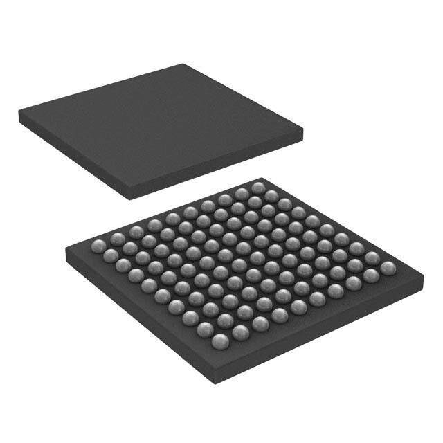
GENERIC PACKAGE VIEW RGE 24 VQFN - 1 mm max height PLASTIC QUAD FLATPACK - NO LEAD Images above are just a representation of the package family, actual package may vary. Refer to the product data sheet for package details. 4204104/H
PACKAGE OUTLINE RGE0024B VQFN - 1 mm max height SCALE 3.000 PLASTIC QUAD FLATPACK - NO LEAD A 4.1 B 3.9 0.5 0.3 PIN 1 INDEX AREA 4.1 3.9 0.3 0.2 DETAIL OPTIONAL TERMINAL TYPICAL C 1 MAX SEATING PLANE 0.05 0.00 0.08 C 2X 2.5 2.45 0.1 (0.2) TYP 7 12 EXPOSED SEE TERMINAL THERMAL PAD DETAIL 6 13 2X 25 SYMM 2.5 1 18 0.3 20X 0.5 24X 0.2 24 SYMM 19 0.1 C A B PIN 1 ID 0.05 (OPTIONAL) 0.5 24X 0.3 4219013/A 05/2017 NOTES: 1. All linear dimensions are in millimeters. Any dimensions in parenthesis are for reference only. Dimensioning and tolerancing per ASME Y14.5M. 2. This drawing is subject to change without notice. 3. The package thermal pad must be soldered to the printed circuit board for thermal and mechanical performance. www.ti.com
EXAMPLE BOARD LAYOUT RGE0024B VQFN - 1 mm max height PLASTIC QUAD FLATPACK - NO LEAD ( 2.45) SYMM 24 19 24X (0.6) 1 18 24X (0.25) (R0.05) TYP 25 SYMM (3.8) 20X (0.5) 13 6 ( 0.2) TYP VIA 7 12 (0.975) TYP (3.8) LAND PATTERN EXAMPLE EXPOSED METAL SHOWN SCALE:15X 0.07 MAX 0.07 MIN ALL AROUND ALL AROUND SOLDER MASK METAL OPENING EXPMOESTEADL SOOPLEDNEINRG MASK EXPMOESTEADL MSOELTDAEL RU NMDAESRK NON SOLDER MASK SOLDER MASK DEFINED DEFINED (PREFERRED) SOLDER MASK DETAILS 4219013/A 05/2017 NOTES: (continued) 4. This package is designed to be soldered to a thermal pad on the board. For more information, see Texas Instruments literature number SLUA271 (www.ti.com/lit/slua271). 5. Vias are optional depending on application, refer to device data sheet. If any vias are implemented, refer to their locations shown on this view. It is recommended that vias under paste be filled, plugged or tented. www.ti.com
EXAMPLE STENCIL DESIGN RGE0024B VQFN - 1 mm max height PLASTIC QUAD FLATPACK - NO LEAD 4X ( 1.08) (0.64) TYP 24 19 24X (0.6) 1 25 18 24X (0.25) (R0.05) TYP (0.64) TYP SYMM (3.8) 20X (0.5) 13 6 METAL TYP 7 12 SYMM (3.8) SOLDER PASTE EXAMPLE BASED ON 0.125 mm THICK STENCIL EXPOSED PAD 25 78% PRINTED SOLDER COVERAGE BY AREA UNDER PACKAGE SCALE:20X 4219013/A 05/2017 NOTES: (continued) 6. Laser cutting apertures with trapezoidal walls and rounded corners may offer better paste release. IPC-7525 may have alternate design recommendations. www.ti.com
IMPORTANTNOTICEANDDISCLAIMER TI PROVIDES TECHNICAL AND RELIABILITY DATA (INCLUDING DATASHEETS), DESIGN RESOURCES (INCLUDING REFERENCE DESIGNS), APPLICATION OR OTHER DESIGN ADVICE, WEB TOOLS, SAFETY INFORMATION, AND OTHER RESOURCES “AS IS” AND WITH ALL FAULTS, AND DISCLAIMS ALL WARRANTIES, EXPRESS AND IMPLIED, INCLUDING WITHOUT LIMITATION ANY IMPLIED WARRANTIES OF MERCHANTABILITY, FITNESS FOR A PARTICULAR PURPOSE OR NON-INFRINGEMENT OF THIRD PARTY INTELLECTUAL PROPERTY RIGHTS. These resources are intended for skilled developers designing with TI products. You are solely responsible for (1) selecting the appropriate TI products for your application, (2) designing, validating and testing your application, and (3) ensuring your application meets applicable standards, and any other safety, security, or other requirements. These resources are subject to change without notice. TI grants you permission to use these resources only for development of an application that uses the TI products described in the resource. Other reproduction and display of these resources is prohibited. No license is granted to any other TI intellectual property right or to any third party intellectual property right. TI disclaims responsibility for, and you will fully indemnify TI and its representatives against, any claims, damages, costs, losses, and liabilities arising out of your use of these resources. TI’s products are provided subject to TI’s Terms of Sale (www.ti.com/legal/termsofsale.html) or other applicable terms available either on ti.com or provided in conjunction with such TI products. TI’s provision of these resources does not expand or otherwise alter TI’s applicable warranties or warranty disclaimers for TI products. Mailing Address: Texas Instruments, Post Office Box 655303, Dallas, Texas 75265 Copyright © 2020, Texas Instruments Incorporated