ICGOO在线商城 > 集成电路(IC) > 嵌入式 - 微控制器 - 应用特定 > MSP430BT5190IPZR

 Datasheet下载
- 型号: MSP430BT5190IPZR
- 制造商: Texas Instruments
- 库位|库存: xxxx|xxxx
- 要求:
| 数量阶梯 | 香港交货 | 国内含税 |
| +xxxx | $xxxx | ¥xxxx |
查看当月历史价格
查看今年历史价格
MSP430BT5190IPZR产品简介:
ICGOO电子元器件商城为您提供MSP430BT5190IPZR由Texas Instruments设计生产,在icgoo商城现货销售,并且可以通过原厂、代理商等渠道进行代购。 MSP430BT5190IPZR价格参考。Texas InstrumentsMSP430BT5190IPZR封装/规格:嵌入式 - 微控制器 - 应用特定, 。您可以下载MSP430BT5190IPZR参考资料、Datasheet数据手册功能说明书,资料中有MSP430BT5190IPZR 详细功能的应用电路图电压和使用方法及教程。
Texas Instruments(德州仪器)的MSP430BT5190IPZR是一款专为低功耗、高性能嵌入式应用设计的应用特定微控制器。它属于MSP430系列,特别适用于蓝牙低功耗(BLE)通信和各种物联网(IoT)应用场景。

 应用场景

1. 智能家居设备:
   - MSP430BT5190IPZR可以用于智能灯泡、智能插座、智能门锁等设备中。通过集成的BLE模块,用户可以通过智能手机或其他BLE设备进行远程控制和监控。其低功耗特性使得这些设备可以在电池供电的情况下长时间运行,减少了频繁更换电池的需求。

2. 可穿戴设备:
   - 该微控制器适合应用于健康监测手环、智能手表等可穿戴设备。它可以与传感器配合,实时采集心率、步数、睡眠质量等数据,并通过BLE传输到手机或云端进行分析。其低功耗设计有助于延长设备的续航时间。

3. 工业自动化:
   - 在工业环境中,MSP430BT5190IPZR可用于无线传感器节点、数据采集终端等设备。它能够通过BLE与其他设备或网关通信,实现远程监控和数据传输。其强大的处理能力和丰富的外设接口,使其能够适应复杂的工业环境需求。

4. 医疗设备:
   - 该微控制器可用于便携式医疗设备,如血糖仪、血压计等。它可以通过BLE将测量结果发送到医生的设备或医院系统,方便患者和医护人员进行健康管理。其低功耗和高可靠性确保了设备的稳定性和长时间使用。

5. 资产追踪与物流管理:
   - 在物流和供应链管理中,MSP430BT5190IPZR可以用于资产标签、货物追踪器等设备。它可以通过BLE与基站或移动设备通信,实时报告位置和状态信息,帮助提高物流效率和安全性。

6. 农业与环境监测:
   - 该微控制器可用于农业领域的土壤湿度传感器、气象站等设备。它可以通过BLE将数据传输到中央控制系统,帮助农民优化灌溉和施肥策略,提高农作物产量。同时,其低功耗特性使得这些设备可以在偏远地区长时间工作。

总之,MSP430BT5190IPZR凭借其低功耗、高性能和内置BLE功能,在多个领域具有广泛的应用前景,特别适合需要无线通信和长时间稳定运行的嵌入式系统。
| 参数 | 数值 |
| 产品目录 | 集成电路 (IC) |
| 描述 | IC MCU 16BIT 256KB FLASH 100LQFP |
| 产品分类 | |
| I/O数 | 87 |
| 品牌 | Texas Instruments |
| 数据手册 | |
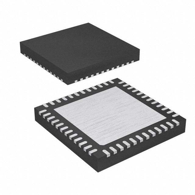
| 产品图片 |
|
| 产品型号 | MSP430BT5190IPZR |
| PCN设计/规格 | |
| RAM容量 | 16K x 8 |
| rohs | 无铅 / 符合限制有害物质指令(RoHS)规范要求 |
| 产品系列 | MSP430 |
| 产品培训模块 | http://www.digikey.cn/PTM/IndividualPTM.page?site=cn&lang=zhs&ptm=25523http://www.digikey.cn/PTM/IndividualPTM.page?site=cn&lang=zhs&ptm=25524http://www.digikey.cn/PTM/IndividualPTM.page?site=cn&lang=zhs&ptm=25537http://www.digikey.cn/PTM/IndividualPTM.page?site=cn&lang=zhs&ptm=25788http://www.digikey.cn/PTM/IndividualPTM.page?site=cn&lang=zhs&ptm=25882http://www.digikey.cn/PTM/IndividualPTM.page?site=cn&lang=zhs&ptm=25885http://www.digikey.cn/PTM/IndividualPTM.page?site=cn&lang=zhs&ptm=26015http://www.digikey.cn/PTM/IndividualPTM.page?site=cn&lang=zhs&ptm=26006 |
| 供应商器件封装 | 100-LQFP(14x14) |
| 其它名称 | 296-28149-6 |
| 制造商产品页 | http://www.ti.com/general/docs/suppproductinfo.tsp?distId=10&orderablePartNumber=MSP430BT5190IPZR |
| 包装 | Digi-Reel® |
| 安装类型 | 表面贴装 |
| 封装/外壳 | 100-LQFP |
| 工作温度 | -40°C ~ 85°C |
| 应用 | 蓝牙 |
| 接口 | I²C, IrDA, SCI, SPI, UART/USART |
| 控制器系列 | MSP430 |
| 标准包装 | 1 |
| 核心处理器 | - |
| 电压-电源 | 1.8 V ~ 3.6 V |
| 程序存储器类型 | 闪存(256 kB) |


- 商务部:美国ITC正式对集成电路等产品启动337调查
- 曝三星4nm工艺存在良率问题 高通将骁龙8 Gen1或转产台积电
- 太阳诱电将投资9.5亿元在常州建新厂生产MLCC 预计2023年完工
- 英特尔发布欧洲新工厂建设计划 深化IDM 2.0 战略
- 台积电先进制程称霸业界 有大客户加持明年业绩稳了
- 达到5530亿美元!SIA预计今年全球半导体销售额将创下新高
- 英特尔拟将自动驾驶子公司Mobileye上市 估值或超500亿美元
- 三星加码芯片和SET,合并消费电子和移动部门,撤换高东真等 CEO
- 三星电子宣布重大人事变动 还合并消费电子和移动部门
- 海关总署:前11个月进口集成电路产品价值2.52万亿元 增长14.8%


PDF Datasheet 数据手册内容提取
Product Sample & Technical Tools & Support & Folder Buy Documents Software Community MSP430BT5190 SLAS703B–APRIL2010–REVISEDAUGUST2015 MSP430BT5190 Mixed-Signal Microcontroller 1 Device Overview 1.1 Features 1 • DesignedforUseWithCC2560TIBluetooth® • UnifiedClockSystem BasedSolutions (1) – FLLControlLoopforFrequencyStabilization • CommerciallyLicensedMindtree™Ethermind – Low-PowerLow-FrequencyInternalClock BluetoothStackforMSP430 Source(VLO) – Bluetoothv2.1+EnhancedDataRate(EDR) – Low-FrequencyTrimmedInternalReference Compliant Source(REFO) – SerialPortProfile(SPP) – 32-kHzCrystals – SampleApplications – High-FrequencyCrystalsupto32MHz • LowSupplyVoltageRange: • 16-BitTimerTA0,Timer_AWithFive 3.6VDownto1.8V Capture/CompareRegisters • Ultra-LowPowerConsumption • 16-BitTimerTA1,Timer_AWithThree – ActiveMode(AM): Capture/CompareRegisters AllSystemClocksActive • 16-BitTimerTB0,Timer_BWithSeven 230µA/MHzat8MHz,3V,FlashProgram Capture/CompareShadowRegisters Execution(Typical) • UptoFourUniversalSerialCommunication 110µA/MHzat8MHz,3V,RAMProgram Interfaces(USCIs) Execution(Typical) – USCI_A0,USCI_A1,USCI_A2,andUSCI_A3 – StandbyMode(LPM3): EachSupport: Real-TimeClock(RTC)WithCrystal,Watchdog, • EnhancedUARTSupportsAutomaticBaud- andSupplySupervisorOperational,FullRAM RateDetection Retention,FastWake-Up: • IrDAEncoderandDecoder 1.7 µAat2.2V,2.1 µAat3V(Typical) Low-PowerOscillator(VLO),General-Purpose • SynchronousSPI Counter,Watchdog,andSupplySupervisor – USCI_B0,USCI_B1,USCI_B2,andUSCI_B3 Operational,FullRAMRetention,FastWakeup: EachSupport: 1.2 µAat3V(Typical) • I2C – OffMode(LPM4): • SynchronousSPI FullRAMRetention,SupplySupervisor • 12-BitAnalog-to-DigitalConverter(ADC) Operational,FastWakeup: – InternalReference 1.2 µAat3V(Typical) – 14ExternalChannels,2InternalChannels – ShutdownMode(LPM4.5): • HardwareMultiplierSupports32-BitOperations 0.1 µAat3V(Typical) • SerialOnboardProgramming,NoExternal • WakeupFromStandbyModeinLessThan5µs ProgrammingVoltageNeeded • 16-BitRISCArchitecture • 3-ChannelInternalDMA • FlexiblePower-ManagementSystem • BasicTimerWithRTCFeature – FullyIntegratedLDOWithProgrammable • ForCompleteModuleDescriptions,Seethe RegulatedCoreSupplyVoltage MSP430x5xxandMSP430x6xxFamilyUser's – SupplyVoltageSupervision,Monitoring,and Guide(SLAU208) Brownout (1) TheBluetoothwordmarkandlogosareownedbyBluetooth SIG,Inc.,andanyuseofsuchmarksbyTIisunderlicense. 1.2 Applications • RemoteControls • BloodGlucoseMeters • Thermostats • Pulseoximeters • SmartMeters 1 AnIMPORTANTNOTICEattheendofthisdatasheetaddressesavailability,warranty,changes,useinsafety-criticalapplications, intellectualpropertymattersandotherimportantdisclaimers.PRODUCTIONDATA.
MSP430BT5190 SLAS703B–APRIL2010–REVISEDAUGUST2015 www.ti.com 1.3 Description The TI MSP430™ family of ultra-low-power microcontrollers consists of several devices featuring different sets of peripherals targeted for various applications. The architecture, combined with extensive low-power modes, is optimized to achieve extended battery life in portable measurement applications. The device features a powerful 16-bit RISC CPU, 16-bit registers, and constant generators that contribute to maximum code efficiency. The digitally controlled oscillator (DCO) allows the device to wake up from low- powermodestoactivemodeinlessthan5µs. MSP430BT5190isamicrocontrollerconfigurationwiththree16-bittimers,ahigh-performance12-bitADC, fourUSCIs,ahardwaremultiplier,DMA,anRTCmodulewithalarmcapabilities,and87I/Opins. The MSP430BT5190 microcontroller is designed for commercial use with TI’s CC2560 based Bluetooth solutions in conjunction with Mindtree’s Ethermind Bluetooth stack and SPP. This MSP430BT5190+CC2560 Bluetooth platform is ideal for applications that need a wireless serial link for cable replacement, such as remote controls, thermostats, smart meters, blood glucose meters, pulseoximeters,andmanyothers. DeviceInformation(1) PARTNUMBER PACKAGE BODYSIZE(2) MSP430BT5190IZQW MicroStarJunior™BGA(113) 7mm×7mm MSP430BT5190IPZ LQFP(100) 14mm×14mm (1) Forthemostcurrentpart,package,andorderinginformation,seethePackageOptionAddendumin Section8,orseetheTIwebsiteatwww.ti.com. (2) Thesizesshownhereareapproximations.Forthepackagedimensionswithtolerances,seethe MechanicalDatainSection8. 1.4 Functional Block Diagram Figure1-1showsthefunctionalblockdiagram. XIN XOUT DVCC DVSS AVCC AVSS RST/NMI PA PB PC PD PE PF P1.x P2.x P3.x P4.x P5.x P6.x P7.x P8.x P9.x P10.x P11.x XT2IN I/O Ports Unified ACLK Power P1/P2 I/O Ports I/O Ports I/O Ports I/O Ports I/O Ports XT2OUT SCylsotcekm SMCLK 256KB 16KB Management SYS I2n×te8r Ir/uOpst 2×P83 /IP/O4s 2×P85 /IP/O6s 2×P87 /IP/O8s 2P×98/ PI/1O0s 1×P3 1I1/Os Capability LDO Watchdog MCLK Flash RAM SVM/SVS PA PB PC PD PE PF Brownout 1×16 I/Os 1×16 I/Os 1×16 I/Os 1×16 I/Os 1×16 I/Os 1×3 I/Os MAB CPUXV2 DMA and Working MDB 3 Channel Registers EEM (L: 8+2) USCI0,1,2,3 ADC12_A JTAG/ TA0 TA1 TB0 USCI_Ax: 12 Bit IntSeBrfWace MPY32 Timer_A Timer_A Timer_B RTC_A CRC16 IrDUAA,R ST,PI 200 KSPS REF 5 CC 3 CC 7 CC 16 Channels Registers Registers Registers UCSI_Bx: (14 ext/2 int) SPI, I2C Autoscan Figure1-1.FunctionalBlockDiagram 2 DeviceOverview Copyright©2010–2015,TexasInstrumentsIncorporated SubmitDocumentationFeedback ProductFolderLinks:MSP430BT5190
MSP430BT5190 www.ti.com SLAS703B–APRIL2010–REVISEDAUGUST2015 Table of Contents 1 DeviceOverview......................................... 1 5.27 Wake-upTimesFromLow-PowerModesand ................................................ .............................................. Reset 28 1.1 Features 1 ............................................. ........................................... 5.28 Timer_A 29 1.2 Applications 1 ............................................. ............................................ 5.29 Timer_B 29 1.3 Description 2 ............................ 5.30 USCI(UARTMode),RecommendedOperating 1.4 FunctionalBlockDiagram 2 ........................................... Conditions 29 2 Revision History......................................... 4 ................................. 5.31 USCI(UARTMode) 29 3 Device Characteristics.................................. 5 5.32 USCI(SPIMasterMode),RecommendedOperating 4 TerminalConfigurationandFunctions.............. 6 Conditions........................................... 30 4.1 PinDiagrams......................................... 6 5.33 USCI(SPIMasterMode)............................ 30 4.2 SignalDescriptions................................... 8 5.34 USCI(SPISlaveMode)............................. 32 5 Specifications........................................... 13 5.35 USCI(I2CMode).................................... 34 ........................ 5.1 AbsoluteMaximumRatings 13 5.36 12-BitADC,PowerSupplyandInputRange 5.2 ESDRatings........................................ 13 Conditions........................................... 35 5.3 RecommendedOperatingConditions............... 13 5.37 12-BitADC,TimingParameters .................... 35 ................... 5.4 ActiveModeSupplyCurrentIntoV Excluding 5.38 12-BitADC,LinearityParameters 35 CC ..................................... External Current 14 5.39 12-BitADC,TemperatureSensorandBuilt-InV 36 MID 5.5 Low-PowerModeSupplyCurrents(IntoV ) ........................... CC 5.40 REF,ExternalReference 37 .......................... ExcludingExternalCurrent 15 ............................. 5.41 REF,Built-InReference 37 ............................. 5.6 Thermal Characteristics 15 ....................................... 5.42 FlashMemory 38 ...... 5.7 Schmitt-TriggerInputs–General-PurposeI/O 16 .................... 5.43 JTAGandSpy-Bi-WireInterface 39 ........................... 5.8 Inputs–PortsP1andP2 16 6 DetailedDescription................................... 40 ........... 5.9 LeakageCurrent–General-PurposeI/O 16 ................................................. 6.1 CPU 40 5.10 Outputs–General-PurposeI/O(FullDrive .................................... ............................................ 6.2 OperatingModes 41 Strength) 17 .......................... 5.11 Outputs–General-PurposeI/O(ReducedDrive 6.3 InterruptVectorAddresses 42 ............................................ ............................... Strength) 17 6.4 Memory Organization 43 .......... ............................. 5.12 OutputFrequency–General-PurposeI/O 17 6.5 BootstrapLoader(BSL) 44 5.13 TypicalCharacteristics–Outputs,ReducedDrive 6.6 JTAGOperation..................................... 44 ............................... Strength(PxDS.y=0) 18 ....................................... 6.7 FlashMemory 45 5.14 TypicalCharacteristics–Outputs,FullDrive ................................................. ............................... 6.8 RAM 45 Strength(PxDS.y=1) 19 .......................................... ..... 6.9 Peripherals 46 5.15 CrystalOscillator,XT1,Low-FrequencyMode 20 ............................ .... 6.10 Input/OutputSchematics 67 5.16 CrystalOscillator,XT1,High-FrequencyMode 21 ........................... .............................. 6.11 DeviceDescriptors(TLV) 91 5.17 CrystalOscillator,XT2 22 7 DeviceandDocumentationSupport............... 94 5.18 InternalVery-Low-PowerLow-FrequencyOscillator (VLO)................................................ 23 7.1 DeviceSupport...................................... 94 ............................. 5.19 InternalReference,Low-FrequencyOscillator 7.2 DocumentationSupport 97 (REFO).............................................. 23 7.3 CommunityResources.............................. 97 5.20 DCO Frequency..................................... 24 7.4 Trademarks.......................................... 97 5.21 PMM,Brown-OutReset(BOR)..................... 25 7.5 ElectrostaticDischargeCaution..................... 97 5.22 PMM,CoreVoltage................................. 25 7.6 ExportControlNotice............................... 97 5.23 PMM,SVSHighSide............................... 26 7.7 Glossary............................................. 97 ............................... 5.24 PMM,SVMHighSide 27 8 Mechanical,Packaging,andOrderable 5.25 PMM,SVSLowSide................................ 28 Information.............................................. 98 ............................... 5.26 PMM,SVMLowSide 28 Copyright©2010–2015,TexasInstrumentsIncorporated TableofContents 3 SubmitDocumentationFeedback ProductFolderLinks:MSP430BT5190
MSP430BT5190 SLAS703B–APRIL2010–REVISEDAUGUST2015 www.ti.com 2 Revision History NOTE:Pagenumbersforpreviousrevisionsmaydifferfrompagenumbersinthecurrentversion. ChangesfromAugust5,2013toAugust6,2015 Page • Documentformatandorganizationchangesthroughout,includingadditionofsectionnumbering ....................... 1 • AddedDeviceInformationtable .................................................................................................... 2 • MovedfunctionalblockdiagramtoFigure1-1,FunctionalBlockDiagram.................................................... 2 • AddedSection3,DeviceCharacteristics,andmovedTable3-1toit ......................................................... 5 • AddedsignalnamestoZQWpinout............................................................................................... 7 • AddedSection5,Specifications,andmovedallelectricalandtimingspecificationstoit................................. 13 • AddedSection5.2,ESDRatings.................................................................................................. 13 • AddednotetoC ............................................................................................................... 13 VCORE • MovedSection5.6,ThermalCharacteristics.................................................................................... 15 • ChangedtheTYPvalueofC withTestConditionsof"XTS=0,XCAPx=0"from2pFto1pF..................... 20 L,eff • CorrectedspellingofMRGbitsinsymbolanddescriptionforf parameter........................................ 38 MCLK,MRG • CorrectedspellingofNMIIFGinTable6-6,SystemModuleInterruptVectorRegisters................................... 48 • ChangedP5.3schematic(addedP5SEL.2andXT2BYPASSinputswithANDandORgates)......................... 77 • ChangedP5SEL.3columnfromXto0for"P5.3(I/O)"rows.................................................................. 77 • ChangedP7.1schematic(addedP7SEL.1inputandORgate).............................................................. 82 • ChangedP7SEL.1columnfromXto0for"P7.1(I/O)"rows.................................................................. 82 • AddedSection7andmovedToolsSupport,DeviceNomenclature,ESDCaution,andTrademarkssectionstoit... 94 • AddedSection8 .................................................................................................................... 98 4 RevisionHistory Copyright©2010–2015,TexasInstrumentsIncorporated SubmitDocumentationFeedback ProductFolderLinks:MSP430BT5190
MSP430BT5190 www.ti.com SLAS703B–APRIL2010–REVISEDAUGUST2015 3 Device Characteristics Table3-1summarizesthedevicecharacteristics. Table3-1.DeviceCharacteristics(1)(2) USCI DEVICE FLASH SRAM Timer_A(3) Timer_B(4) CHANNELA: CHANNELB: ADC12_A I/O PACKAGE (KB) (KB) UART,IrDA, SPI,I2C (Ch) SPI 100PZ, MSP430BT5190 256 16 5,3 7 4 4 14ext,2int 87 113ZQW (1) Forthemostcurrentpart,package,andorderinginformation,seethePackageOptionAddenduminSection8,orseetheTIwebsiteat www.ti.com. (2) Packagedrawings,thermaldata,andsymbolizationareavailableatwww.ti.com/packaging. (3) EachnumberinthesequencerepresentsaninstantiationofTimer_Awithitsassociatednumberofcapture/compareregistersandPWM outputgeneratorsavailable.Forexample,anumbersequenceof3,5wouldrepresenttwoinstantiationsofTimer_A,thefirst instantiationhaving3andthesecondinstantiationhaving5capture/compareregistersandPWMoutputgenerators,respectively. (4) EachnumberinthesequencerepresentsaninstantiationofTimer_Bwithitsassociatednumberofcapture/compareregistersandPWM outputgeneratorsavailable.Forexample,anumbersequenceof3,5wouldrepresenttwoinstantiationsofTimer_B,thefirst instantiationhaving3andthesecondinstantiationhaving5capture/compareregistersandPWMoutputgenerators,respectively. Copyright©2010–2015,TexasInstrumentsIncorporated DeviceCharacteristics 5 SubmitDocumentationFeedback ProductFolderLinks:MSP430BT5190
MSP430BT5190 SLAS703B–APRIL2010–REVISEDAUGUST2015 www.ti.com 4 Terminal Configuration and Functions 4.1 Pin Diagrams Figure4-1showsthepinoutofthe100-pinPZpackage. MIMOECLDAK SOSIST3S3SCL 333BB3 AAACCA O CCCUUC 6.3/A36.2/A26.1/A16.0/A0ST/NMI/SBWTDIJ.3/TCKJ.2/TMSJ.1/TDI/TCLKJ.0/TDOEST/SBWTCK5.3/XT2OUT5.2/XT2INVSS4VCC411.2/SMCLK11.1/MCLK11.0/ACLK10.710.610.5/UCA3RXDU10.4/UCA3TXD/U10.3/UCB3CLK/U10.2/UCB3SOMI/10.1/UCB3SIMO/10.0/UCB3STE/U PPPPRPPPPTPPDDPPPPPPPPPPP 09 8 76 5 43 2 1098 7 65 4 3 2 1 09 8 76 09 9 99 9 99 9 9988 8 88 8 8 8 8 87 7 77 P6.4/A4 1 1 75 P9.7 P6.5/A5 2 74 P9.6 P6.6/A6 3 73 P9.5/UCA2RXDUCA2SOMI P6.7/A7 4 72 P9.4/UCA2TXD/UCA2SIMO P7.4/A12 5 71 P9.3/UCB2CLK/UCA2STE P7.5/A13 6 70 P9.2/UCB2SOMI/UCB2SCL P7.6/A14 7 69 P9.1/UCB2SIMO/UCB2SDA P7.7/A15 8 68 P9.0/UCB2STE/UCA2CLK P5.0/A8/VREF+/VeREF+ 9 67 P8.7 P5.1/A9/VREF−/VeREF− 10 66 P8.6/TA1.1 AVCC 11 65 P8.5/TA1.0 AVSS 12 64 DVCC2 P7.0/XIN 13 63 DVSS2 P7.1/XOUT 14 62 VCORE DVSS1 15 61 P8.4/TA0.4 DVCC1 16 60 P8.3/TA0.3 P1.0/TA0CLK/ACLK 17 59 P8.2/TA0.2 P1.1/TA0.0 18 58 P8.1/TA0.1 P1.2/TA0.1 19 57 P8.0/TA0.0 P1.3/TA0.2 20 56 P7.3/TA1.2 P1.4/TA0.3 21 55 P7.2/TB0OUTH/SVMOUT P1.5/TA0.4 22 54 P5.7/UCA1RXD/UCA1SOMI P1.6/SMCLK 23 53 P5.6/UCA1TXD/UCA1SIMO P1.7 24 52 P5.5/UCB1CLK/UCA1STE P2.0/TA1CLK/MCLK 25 51 P5.4/UCB1SOMI/UCB1SCL 6 7 89 01 2 34 5 67 8 90 1 23 4 56 7 89 0 2 2 22 33 3 33 3 33 3 34 4 44 4 44 4 44 5 P2.1/TA1.0P2.2/TA1.1P2.3/TA1.2P2.4/RTCCLKP2.5P2.6/ACLK12CLK/DMAE0STE/UCA0CLKMO/UCB0SDAOMI/UCB0SCLCLK/UCA0STEDVSS3DVCC3 XD/UCA0SIMOXD/UCA0SOMISTE/UCA1CLKMO/UCB1SDAP4.0/TB0.0P4.1/TB0.1P4.2/TB0.2P4.3/TB0.3P4.4/TB0.4P4.5/TB0.5P4.6/TB0.6B0CLK/SMCLK C0SIS0 TR1SI T P2.7/ADP3.0/UCB3.1/UCB03.2/UCB0P3.3/UCB 3.4/UCA03.5/UCA0P3.6/UCB3.7/UCB1 P4.7/ PP PP P Figure4-1.100-PinPZPackage(TopView) 6 TerminalConfigurationandFunctions Copyright©2010–2015,TexasInstrumentsIncorporated SubmitDocumentationFeedback ProductFolderLinks:MSP430BT5190
MSP430BT5190 www.ti.com SLAS703B–APRIL2010–REVISEDAUGUST2015 Figure4-2showsthepinoutofthe113-pinZQWpackage. P6.4 P6.2 RST PJ.1 P5.3 P5.2 P11.2 P11.0 P10.6 P10.4 P10.1 P9.7 A1 A2 A3 A4 A5 A6 A7 A8 A9 A10 A11 A12 P6.6 P6.3 P6.1 PJ.3 PJ.0 DVSS4 DVCC4 P10.7 P10.5 P10.3 P9.6 P9.5 B1 B2 B3 B4 B5 B6 B7 B8 B9 B10 B11 B12 P7.5 P6.7 Reserved P9.4 P9.2 C1 C2 C3 C11 C12 P5.0 P7.6 P6.0 PJ.2 TEST P11.1 P10.2 P10.0 P9.0 P8.7 D1 D2 D4 D5 D6 D7 D8 D9 D11 D12 P5.1 AVCC P6.5 Reserved Reserved Reserved Reserved P9.3 P8.6 DVCC2 E1 E2 E4 E5 E6 E7 E8 E9 E11 E12 P7.0 AVSS P7.4 Reserved Reserved P9.1 P8.5 DVSS2 F1 F2 F4 F5 F8 F9 F11 F12 P7.1 DVSS1 P7.7 Reserved Reserved P8.3 P8.4 VCORE G1 G2 G4 G5 G8 G9 G11 G12 P1.0 DVCC1 P1.1 Reserved Reserved Reserved A8 P8.0 P8.1 P8.2 H1 H2 H4 H5 H6 H7 H8 H9 H11 H12 P1.3 P1.4 P1.2 P2.7 P3.2 P3.5 P4.0 P5.5 P7.2 P7.3 J1 J2 J4 J5 J6 J7 J8 J9 J11 J12 P1.5 P1.6 P5.6 P5.7 K1 K2 K11 K12 P1.7 P2.1 P2.3 P2.5 P3.0 P3.3 P3.4 P3.7 P4.2 P4.3 P4.5 P5.4 L1 L2 L3 L4 L5 L6 L7 L8 L9 L10 L11 L12 P2.0 P2.2 P2.4 P2.6 P3.1 DVSS3 DVCC3 P3.6 P4.1 P4.4 P4.6 P4.7 M1 M2 M3 M4 M5 M6 M7 M8 M9 M10 M11 M12 Figure4-2.113-PinZQWPackage(TopView) Copyright©2010–2015,TexasInstrumentsIncorporated TerminalConfigurationandFunctions 7 SubmitDocumentationFeedback ProductFolderLinks:MSP430BT5190
MSP430BT5190 SLAS703B–APRIL2010–REVISEDAUGUST2015 www.ti.com 4.2 Signal Descriptions Table4-1describesthesignals. Table4-1.TerminalFunctions TERMINAL NO. I/O(1) DESCRIPTION NAME PZ ZQW General-purposedigitalI/O P6.4/A4 1 A1 I/O AnaloginputA4–ADC General-purposedigitalI/O P6.5/A5 2 E4 I/O AnaloginputA5–ADC General-purposedigitalI/O P6.6/A6 3 B1 I/O AnaloginputA6–ADC General-purposedigitalI/O P6.7/A7 4 C2 I/O AnaloginputA7–ADC General-purposedigitalI/O P7.4/A12 5 F4 I/O AnaloginputA12–ADC General-purposedigitalI/O P7.5/A13 6 C1 I/O AnaloginputA13–ADC General-purposedigitalI/O P7.6/A14 7 D2 I/O AnaloginputA14–ADC General-purposedigitalI/O P7.7/A15 8 G4 I/O AnaloginputA15–ADC General-purposedigitalI/O AnaloginputA8–ADC P5.0/A8/VREF+/VeREF+ 9 D1 I/O OutputofreferencevoltagetotheADC InputforanexternalreferencevoltagetotheADC General-purposedigitalI/O AnaloginputA9–ADC P5.1/A9/VREF-/VeREF- 10 E1 I/O NegativeterminalfortheADCreferencevoltageforbothsources,theinternal referencevoltage,oranexternalappliedreferencevoltage AVCC 11 E2 Analogpowersupply AVSS 12 F2 Analoggroundsupply General-purposedigitalI/O P7.0/XIN 13 F1 I/O InputterminalforcrystaloscillatorXT1 General-purposedigitalI/O P7.1/XOUT 14 G1 I/O OutputterminalofcrystaloscillatorXT1 DVSS1 15 G2 Digitalgroundsupply DVCC1 16 H2 Digitalpowersupply General-purposedigitalI/Owithportinterrupt P1.0/TA0CLK/ACLK 17 H1 I/O TA0clocksignalTACLKinput ACLKoutput(dividedby1,2,4,8,16,or32) General-purposedigitalI/Owithportinterrupt P1.1/TA0.0 18 H4 I/O TA0CCR0capture:CCI0Ainput,compare:Out0output BSLtransmitoutput General-purposedigitalI/Owithportinterrupt P1.2/TA0.1 19 J4 I/O TA0CCR1capture:CCI1Ainput,compare:Out1output BSLreceiveinput General-purposedigitalI/Owithportinterrupt P1.3/TA0.2 20 J1 I/O TA0CCR2capture:CCI2Ainput,compare:Out2output General-purposedigitalI/Owithportinterrupt P1.4/TA0.3 21 J2 I/O TA0CCR3capture:CCI3Ainputcompare:Out3output General-purposedigitalI/Owithportinterrupt P1.5/TA0.4 22 K1 I/O TA0CCR4capture:CCI4Ainput,compare:Out4output General-purposedigitalI/Owithportinterrupt P1.6/SMCLK 23 K2 I/O SMCLKoutput P1.7 24 L1 I/O General-purposedigitalI/Owithportinterrupt (1) I=input,O=output,N/A=notavailableonthispackageoffering 8 TerminalConfigurationandFunctions Copyright©2010–2015,TexasInstrumentsIncorporated SubmitDocumentationFeedback ProductFolderLinks:MSP430BT5190
MSP430BT5190 www.ti.com SLAS703B–APRIL2010–REVISEDAUGUST2015 Table4-1.TerminalFunctions(continued) TERMINAL NO. I/O(1) DESCRIPTION NAME PZ ZQW General-purposedigitalI/Owithportinterrupt P2.0/TA1CLK/MCLK 25 M1 I/O TA1clocksignalTA1CLKinput MCLKoutput General-purposedigitalI/Owithportinterrupt P2.1/TA1.0 26 L2 I/O TA1CCR0capture:CCI0Ainput,compare:Out0output General-purposedigitalI/Owithportinterrupt P2.2/TA1.1 27 M2 I/O TA1CCR1capture:CCI1Ainput,compare:Out1output General-purposedigitalI/Owithportinterrupt P2.3/TA1.2 28 L3 I/O TA1CCR2capture:CCI2Ainput,compare:Out2output General-purposedigitalI/Owithportinterrupt P2.4/RTCCLK 29 M3 I/O RTCCLKoutput P2.5 30 L4 I/O General-purposedigitalI/Owithportinterrupt General-purposedigitalI/Owithportinterrupt P2.6/ACLK 31 M4 I/O ACLKoutput(dividedby1,2,4,8,16,or32) General-purposedigitalI/Owithportinterrupt P2.7/ADC12CLK/DMAE0 32 J5 I/O ConversionclockoutputADC DMAexternaltriggerinput General-purposedigitalI/O Slavetransmitenable–USCI_B0SPImode P3.0/UCB0STE/UCA0CLK 33 L5 I/O Clocksignalinput–USCI_A0SPIslavemode Clocksignaloutput–USCI_A0SPImastermode General-purposedigitalI/O P3.1/UCB0SIMO/UCB0SDA 34 M5 I/O Slavein,masterout–USCI_B0SPImode I2Cdata–USCI_B0I2Cmode General-purposedigitalI/O P3.2/UCB0SOMI/UCB0SCL 35 J6 I/O Slaveout,masterin–USCI_B0SPImode I2Cclock–USCI_B0I2Cmode General-purposedigitalI/O Clocksignalinput–USCI_B0SPIslavemode P3.3/UCB0CLK/UCA0STE 36 L6 I/O Clocksignaloutput–USCI_B0SPImastermode Slavetransmitenable–USCI_A0SPImode DVSS3 37 M6 Digitalgroundsupply DVCC3 38 M7 Digitalpowersupply General-purposedigitalI/O P3.4/UCA0TXD/UCA0SIMO 39 L7 I/O Transmitdata–USCI_A0UARTmode Slavein,masterout–USCI_A0SPImode General-purposedigitalI/O P3.5/UCA0RXD/UCA0SOMI 40 J7 I/O Receivedata–USCI_A0UARTmode Slaveout,masterin–USCI_A0SPImode General-purposedigitalI/O Slavetransmitenable–USCI_B1SPImode P3.6/UCB1STE/UCA1CLK 41 M8 I/O Clocksignalinput–USCI_A1SPIslavemode Clocksignaloutput–USCI_A1SPImastermode General-purposedigitalI/O P3.7/UCB1SIMO/UCB1SDA 42 L8 I/O Slavein,masterout–USCI_B1SPImode I2Cdata–USCI_B1I2Cmode General-purposedigitalI/O P4.0/TB0.0 43 J8 I/O TB0captureCCR0:CCI0A/CCI0Binput,compare:Out0output General-purposedigitalI/O P4.1/TB0.1 44 M9 I/O TB0captureCCR1:CCI1A/CCI1Binput,compare:Out1output General-purposedigitalI/O P4.2/TB0.2 45 L9 I/O TB0captureCCR2:CCI2A/CCI2Binput,compare:Out2output General-purposedigitalI/O P4.3/TB0.3 46 L10 I/O TB0captureCCR3:CCI3A/CCI3Binput,compare:Out3output General-purposedigitalI/O P4.4/TB0.4 47 M10 I/O TB0captureCCR4:CCI4A/CCI4Binput,compare:Out4output Copyright©2010–2015,TexasInstrumentsIncorporated TerminalConfigurationandFunctions 9 SubmitDocumentationFeedback ProductFolderLinks:MSP430BT5190
MSP430BT5190 SLAS703B–APRIL2010–REVISEDAUGUST2015 www.ti.com Table4-1.TerminalFunctions(continued) TERMINAL NO. I/O(1) DESCRIPTION NAME PZ ZQW General-purposedigitalI/O P4.5/TB0.5 48 L11 I/O TB0captureCCR5:CCI5A/CCI5Binput,compare:Out5output General-purposedigitalI/O P4.6/TB0.6 49 M11 I/O TB0captureCCR6:CCI6A/CCI6Binput,compare:Out6output General-purposedigitalI/O P4.7/TB0CLK/SMCLK 50 M12 I/O TB0clockinput SMCLKoutput General-purposedigitalI/O P5.4/UCB1SOMI/UCB1SCL 51 L12 I/O Slaveout,masterin–USCI_B1SPImode I2Cclock–USCI_B1I2Cmode General-purposedigitalI/O Clocksignalinput–USCI_B1SPIslavemode P5.5/UCB1CLK/UCA1STE 52 J9 I/O Clocksignaloutput–USCI_B1SPImastermode Slavetransmitenable–USCI_A1SPImode General-purposedigitalI/O P5.6/UCA1TXD/UCA1SIMO 53 K11 I/O Transmitdata–USCI_A1UARTmode Slavein,masterout–USCI_A1SPImode General-purposedigitalI/O P5.7/UCA1RXD/UCA1SOMI 54 K12 I/O Receivedata–USCI_A1UARTmode Slaveout,masterin–USCI_A1SPImode General-purposedigitalI/O P7.2/TB0OUTH/SVMOUT 55 J11 I/O SwitchallPWMoutputshighimpedance–TimerTB0 SVMoutput General-purposedigitalI/O P7.3/TA1.2 56 J12 I/O TA1CCR2capture:CCI2Binput,compare:Out2output General-purposedigitalI/O P8.0/TA0.0 57 H9 I/O TA0CCR0capture:CCI0Binput,compare:Out0output General-purposedigitalI/O P8.1/TA0.1 58 H11 I/O TA0CCR1capture:CCI1Binput,compare:Out1output General-purposedigitalI/O P8.2/TA0.2 59 H12 I/O TA0CCR2capture:CCI2Binput,compare:Out2output General-purposedigitalI/O P8.3/TA0.3 60 G9 I/O TA0CCR3capture:CCI3Binput,compare:Out3output General-purposedigitalI/O P8.4/TA0.4 61 G11 I/O TA0CCR4capture:CCI4Binput,compare:Out4output VCORE(2) 62 G12 Regulatedcorepowersupplyoutput(internaluseonly,noexternalcurrentloading) DVSS2 63 F12 Digitalgroundsupply DVCC2 64 E12 Digitalpowersupply General-purposedigitalI/O P8.5/TA1.0 65 F11 I/O TA1CCR0capture:CCI0Binput,compare:Out0output General-purposedigitalI/O P8.6/TA1.1 66 E11 I/O TA1CCR1capture:CCI1Binput,compare:Out1output P8.7 67 D12 I/O General-purposedigitalI/O General-purposedigitalI/O Slavetransmitenable–USCI_B2SPImode P9.0/UCB2STE/UCA2CLK 68 D11 I/O Clocksignalinput–USCI_A2SPIslavemode Clocksignaloutput–USCI_A2SPImastermode General-purposedigitalI/O P9.1/UCB2SIMO/UCB2SDA 69 F9 I/O Slavein,masterout–USCI_B2SPImode I2Cdata–USCI_B2I2Cmode General-purposedigitalI/O P9.2/UCB2SOMI/UCB2SCL 70 C12 I/O Slaveout,masterin–USCI_B2SPImode I2Cclock–USCI_B2I2Cmode (2) VCOREisforinternaluseonly.Noexternalcurrentloadingispossible.VCOREshouldonlybeconnectedtotherecommended capacitorvalue,C . VCORE 10 TerminalConfigurationandFunctions Copyright©2010–2015,TexasInstrumentsIncorporated SubmitDocumentationFeedback ProductFolderLinks:MSP430BT5190
MSP430BT5190 www.ti.com SLAS703B–APRIL2010–REVISEDAUGUST2015 Table4-1.TerminalFunctions(continued) TERMINAL NO. I/O(1) DESCRIPTION NAME PZ ZQW General-purposedigitalI/O Clocksignalinput–USCI_B2SPIslavemode P9.3/UCB2CLK/UCA2STE 71 E9 I/O Clocksignaloutput–USCI_B2SPImastermode Slavetransmitenable–USCI_A2SPImode General-purposedigitalI/O P9.4/UCA2TXD/UCA2SIMO 72 C11 I/O Transmitdata–USCI_A2UARTmode Slavein,masterout–USCI_A2SPImode General-purposedigitalI/O P9.5/UCA2RXD/UCA2SOMI 73 B12 I/O Receivedata–USCI_A2UARTmode Slaveout,masterin–USCI_A2SPImode P9.6 74 B11 I/O General-purposedigitalI/O P9.7 75 A12 I/O General-purposedigitalI/O General-purposedigitalI/O Slavetransmitenable–USCI_B3SPImode P10.0/UCB3STE/UCA3CLK 76 D9 I/O Clocksignalinput–USCI_A3SPIslavemode Clocksignaloutput–USCI_A3SPImastermode General-purposedigitalI/O P10.1/UCB3SIMO/UCB3SDA 77 A11 I/O Slavein,masterout–USCI_B3SPImode I2Cdata–USCI_B3I2Cmode General-purposedigitalI/O P10.2/UCB3SOMI/UCB3SCL 78 D8 I/O Slaveout,masterin–USCI_B3SPImode I2Cclock–USCI_B3I2Cmode General-purposedigitalI/O Clocksignalinput–USCI_B3SPIslavemode P10.3/UCB3CLK/UCA3STE 79 B10 I/O Clocksignaloutput–USCI_B3SPImastermode Slavetransmitenable–USCI_A3SPImode General-purposedigitalI/O P10.4/UCA3TXD/UCA3SIMO 80 A10 I/O Transmitdata–USCI_A3UARTmode Slavein,masterout–USCI_A3SPImode General-purposedigitalI/O P10.5/UCA3RXD/UCA3SOMI 81 B9 I/O Receivedata–USCI_A3UARTmode Slaveout,masterin–USCI_A3SPImode P10.6 82 A9 I/O General-purposedigitalI/O P10.7 83 B8 I/O General-purposedigitalI/O General-purposedigitalI/O P11.0/ACLK 84 A8 I/O ACLKoutput(dividedby1,2,4,8,16,or32) General-purposedigitalI/O P11.1/MCLK 85 D7 I/O MCLKoutput General-purposedigitalI/O P11.2/SMCLK 86 A7 I/O SMCLKoutput DVCC4 87 B7 Digitalpowersupply DVSS4 88 B6 Digitalgroundsupply General-purposedigitalI/O P5.2/XT2IN 89 A6 I/O InputterminalforcrystaloscillatorXT2 General-purposedigitalI/O P5.3/XT2OUT 90 A5 I/O OutputterminalofcrystaloscillatorXT2 TEST/SBWTCK(3) 91 D6 I Testmodepin–SelectsfourwireJTAGoperation. Spy-Bi-WireinputclockwhenSpy-Bi-Wireoperationactivated PJ.0/TDO(4) 92 B5 I/O General-purposedigitalI/O JTAGtestdataoutputport PJ.1/TDI/TCLK(4) 93 A4 I/O General-purposedigitalI/O JTAGtestdatainputortestclockinput (3) SeeSection6.5andSection6.6forusewithBSLandJTAGfunctions,respectively. (4) SeeSection6.6forusewithJTAGfunction. Copyright©2010–2015,TexasInstrumentsIncorporated TerminalConfigurationandFunctions 11 SubmitDocumentationFeedback ProductFolderLinks:MSP430BT5190
MSP430BT5190 SLAS703B–APRIL2010–REVISEDAUGUST2015 www.ti.com Table4-1.TerminalFunctions(continued) TERMINAL NO. I/O(1) DESCRIPTION NAME PZ ZQW PJ.2/TMS(4) 94 D5 I/O General-purposedigitalI/O JTAGtestmodeselect PJ.3/TCK(4) 95 B4 I/O General-purposedigitalI/O JTAGtestclock Resetinputactivelow(5) RST/NMI/SBWTDIO(3) 96 A3 I/O Nonmaskableinterruptinput Spy-Bi-Wiredatainput/outputwhenSpy-Bi-Wireoperationactivated. General-purposedigitalI/O P6.0/A0 97 D4 I/O AnaloginputA0–ADC General-purposedigitalI/O P6.1/A1 98 B3 I/O AnaloginputA1–ADC General-purposedigitalI/O P6.2/A2 99 A2 I/O AnaloginputA2–ADC General-purposedigitalI/O P6.3/A3 100 B2 I/O AnaloginputA3–ADC G5, E8, F8, G8, H8, E7, Reserved N/A H7, Reserved.Connecttoground. E6, H6, E5, F5, H5, C3 (5) Whenthispinisconfiguredasreset,theinternalpullupresistorisenabledbydefault. 12 TerminalConfigurationandFunctions Copyright©2010–2015,TexasInstrumentsIncorporated SubmitDocumentationFeedback ProductFolderLinks:MSP430BT5190
MSP430BT5190 www.ti.com SLAS703B–APRIL2010–REVISEDAUGUST2015 5 Specifications 5.1 Absolute Maximum Ratings(1) overoperatingfree-airtemperaturerange(unlessotherwisenoted) MIN MAX UNIT VoltageappliedatV toV –0.3 4.1 V CC SS Voltageappliedtoanypin(excludingVCORE)(2) –0.3 V +0.3 V CC Diodecurrentatanydevicepin ±2 mA Storagetemperaturerange,T (3) –55 105 °C stg Maximumjunctiontemperature,T 95 °C J (1) StressesbeyondthoselistedunderAbsoluteMaximumRatingsmaycausepermanentdamagetothedevice.Thesearestressratings only,andfunctionaloperationofthedeviceattheseoranyotherconditionsbeyondthoseindicatedunderRecommendedOperating Conditionsisnotimplied.Exposuretoabsolute-maximum-ratedconditionsforextendedperiodsmayaffectdevicereliability. (2) AllvoltagesreferencedtoV .VCOREisforinternaldeviceuseonly.NoexternalDCloadingorvoltageshouldbeapplied. SS (3) HighertemperaturemaybeappliedduringboardsolderingaccordingtothecurrentJEDECJ-STD-020specificationwithpeakreflow temperaturesnothigherthanclassifiedonthedevicelabelontheshippingboxesorreels. 5.2 ESD Ratings VALUE UNIT Human-bodymodel(HBM),perANSI/ESDA/JEDECJS-001(1) ±1000 V Electrostaticdischarge V (ESD) Charged-devicemodel(CDM),perJEDECspecificationJESD22-C101(2) ±250 (1) JEDECdocumentJEP155statesthat500-VHBMallowssafemanufacturingwithastandardESDcontrolprocess.Pinslistedas ±1000Vmayactuallyhavehigherperformance. (2) JEDECdocumentJEP157statesthat250-VCDMallowssafemanufacturingwithastandardESDcontrolprocess.Pinslistedas±250V mayactuallyhavehigherperformance. 5.3 Recommended Operating Conditions TypicalvaluesarespecifiedatV =3.3VandT =25°C(unlessotherwisenoted) CC A MIN NOM MAX UNIT Supplyvoltageduringprogramexecutionandflashprogramming VCC (AV =DV =DV )(1)(2) 1.8 3.6 V CC CC1/2/3/4 CC V Supplyvoltage(AV =DV =DV ) 0 V SS SS SS1/2/3/4 SS T Operatingfree-airtemperature Iversion –40 85 °C A T Operatingjunctiontemperature Iversion –40 85 °C J C RecommendedcapacitoratVCORE(3) 470 nF VCORE C /C DVCC V CapacitorratioofDVCCtoVCORE 10 CORE PMMCOREVx=0,1.8V≤V ≤3.6V 0 8.0 CC Processorfrequency(maximumMCLK PMMCOREVx=1,2.0V≤VCC≤3.6V 0 12.0 fSYSTEM frequency)(4)(5)(seeFigure5-1) PMMCOREVx=2,2.2V≤V ≤3.6V 0 20.0 MHz CC PMMCOREVx=3,2.4V≤V ≤3.6V 0 25.0 CC (1) TIrecommendspoweringAVCCandDVCCfromthesamesource.Amaximumdifferenceof0.3VbetweenAVCCandDVCCcanbe toleratedduringpowerupandoperation. (2) TheminimumsupplyvoltageisdefinedbythesupervisorSVSlevelswhenitisenabled.SeetheSection5.23thresholdparametersfor theexactvaluesandfurtherdetails. (3) Acapacitortoleranceof±20%orbetterisrequired. (4) TheMSP430CPUisclockeddirectlywithMCLK.BoththehighandlowphaseofMCLKmustnotexceedthepulsedurationofthe specifiedmaximumfrequency. (5) Modulesmayhaveadifferentmaximuminputclockspecification.Seethespecificationoftherespectivemoduleinthisdatasheet. Copyright©2010–2015,TexasInstrumentsIncorporated Specifications 13 SubmitDocumentationFeedback ProductFolderLinks:MSP430BT5190
MSP430BT5190 SLAS703B–APRIL2010–REVISEDAUGUST2015 www.ti.com 25 3 20 z H M 2 2, 3 y - c n 12 e u q e 1 1, 2 1, 2, 3 Fr m 8 e st y S 0 0, 1 0, 1, 2 0, 1, 2, 3 0 1.8 2.0 2.2 2.4 3.6 Supply Voltage - V The numbers within the fields denote the supported PMMCOREVx settings. Figure5-1.FrequencyvsSupplyVoltage 5.4 Active Mode Supply Current Into V Excluding External Current CC overrecommendedoperatingfree-airtemperature(unlessotherwisenoted)(1) (2) (3) FREQUENCY(f =f =f ) DCO MCLK SMCLK EXECUTION PARAMETER V PMMCOREVx 1MHz 8MHz 12MHz 20MHz 25MHz UNIT MEMORY CC TYP MAX TYP MAX TYP MAX TYP MAX TYP MAX 0 0.29 0.33 1.84 2.08 1 0.32 2.08 3.10 I Flash 3V mA AM,Flash 2 0.33 2.24 3.50 6.37 3 0.35 2.36 3.70 6.75 8.90 9.60 0 0.17 0.19 0.88 0.99 1 0.18 1.00 1.47 I RAM 3V mA AM,RAM 2 0.19 1.13 1.68 2.82 3 0.20 1.20 1.78 3.00 4.50 4.90 (1) Allinputsaretiedto0VortoV .Outputsdonotsourceorsinkanycurrent. CC (2) ThecurrentsarecharacterizedwithaMicroCrystalMS1V-T1Kcrystalwithaloadcapacitanceof12.5pF.Theinternalandexternalload capacitancearechosentocloselymatchtherequired12.5pF. (3) Characterizedwithprogramexecutingtypicaldataprocessing. f =32786Hz,f =f =f atspecifiedfrequency. ACLK DCO MCLK SMCLK XTS=CPUOFF=SCG0=SCG1=OSCOFF=SMCLKOFF=0. 14 Specifications Copyright©2010–2015,TexasInstrumentsIncorporated SubmitDocumentationFeedback ProductFolderLinks:MSP430BT5190
MSP430BT5190 www.ti.com SLAS703B–APRIL2010–REVISEDAUGUST2015 5.5 Low-Power Mode Supply Currents (Into V ) Excluding External Current CC overrecommendedrangesofsupplyvoltageandoperatingfree-airtemperature(unlessotherwisenoted)(1) (2) –40°C 25°C 60°C 85°C PARAMETER V PMMCOREVx UNIT CC TYP MAX TYP MAX TYP MAX TYP MAX Low-power 2.2V 0 69 93 69 93 69 93 69 93 ILPM0,1MHz mode0(3) (4) 3V 3 73 100 73 100 73 100 73 100 µA Low-power 2.2V 0 11 15.5 11 15.5 11 15.5 11 15.5 ILPM2 mode2(5) (4) 3V 3 11.7 17.5 11.7 17.5 11.7 17.5 11.7 17.5 µA 0 1.4 1.7 2.6 6.6 2.2V 1 1.5 1.8 2.9 9.9 2 1.5 2.0 3.3 10.1 Low-powermode3, ILPM3,XT1LF crystalmode(6) (4) 0 1.8 2.1 2.4 2.8 7.1 13.6 µA 1 1.8 2.3 3.1 10.5 3V 2 1.9 2.4 3.5 10.6 3 2.0 2.3 2.6 3.9 11.8 14.8 0 1.0 1.2 1.42 2.0 5.8 12.9 Low-powermode3, 1 1.0 1.3 2.3 6.0 ILPM3,VLO VLOmode(7) (4) 3V 2 1.1 1.4 2.8 6.2 µA 3 1.2 1.4 1.62 3.0 6.2 13.9 0 1.1 1.2 1.35 1.9 5.7 12.9 Low-power 1 1.2 1.2 2.2 5.9 ILPM4 mode4(8) (4) 3V 2 1.3 1.3 2.6 6.1 µA 3 1.3 1.3 1.52 2.9 6.2 13.9 I Low-powermode4.5(9) 3V 0.10 0.10 0.13 0.20 0.50 1.14 µA LPM4.5 (1) Allinputsaretiedto0VortoV .Outputsdonotsourceorsinkanycurrent. CC (2) ThecurrentsarecharacterizedwithaMicroCrystalMS1V-T1Kcrystalwithaloadcapacitanceof12.5pF.Theinternalandexternalload capacitancearechosentocloselymatchtherequired12.5pF. (3) CurrentforwatchdogtimerclockedbySMCLKincluded.ACLK=lowfrequencycrystaloperation(XTS=0,XT1DRIVEx=0). CPUOFF=1,SCG0=0,SCG1=0,OSCOFF=0(LPM0),f =32768Hz,f =0MHz,f =f =1MHz ACLK MCLK SMCLK DCO (4) Currentforbrownout,highsidesupervisor(SVS )normalmodeincluded.Low-sidesupervisorandmonitorsdisabled(SVS ,SVM ). H L L Highsidemonitordisabled(SVM ).RAMretentionenabled. H (5) CurrentforwatchdogtimerandRTCclockedbyACLKincluded.ACLK=lowfrequencycrystaloperation(XTS=0,XT1DRIVEx=0). CPUOFF=1,SCG0=0,SCG1=1,OSCOFF=0(LPM2),f =32768Hz,f =0MHz,f =f =0MHz,DCOsetting= ACLK MCLK SMCLK DCO 1MHzoperation,DCObiasgeneratorenabled. (6) CurrentforwatchdogtimerandRTCclockedbyACLKincluded.ACLK=lowfrequencycrystaloperation(XTS=0,XT1DRIVEx=0). CPUOFF=1,SCG0=1,SCG1=1,OSCOFF=0(LPM3),f =32768Hz,f =f =f =0MHz ACLK MCLK SMCLK DCO (7) CurrentforwatchdogtimerandRTCclockedbyACLKincluded.ACLK=VLO. CPUOFF=1,SCG0=1,SCG1=1,OSCOFF=0(LPM3),f =f ,f =f =f =0MHz ACLK VLO MCLK SMCLK DCO (8) CPUOFF=1,SCG0=1,SCG1=1,OSCOFF=1(LPM4),f =f = f =f =0MHz DCO ACLK MCLK SMCLK (9) Internalregulatordisabled.Nodataretention. CPUOFF=1,SCG0=1,SCG1=1,OSCOFF=1,PMMREGOFF=1(LPM4.5),f =f = f =f =0MHz DCO ACLK MCLK SMCLK 5.6 Thermal Characteristics VALUE UNIT QFP(PZ) 50.1 Low-Kboard(JESD51-3) BGA(ZQW) 60 θ Junction-to-ambientthermalresistance,stillair °C/W JA QFP(PZ) 40.8 High-Kboard(JESD51-7) BGA(ZQW) 42 QFP(PZ) 8.9 θ Junction-to-casethermalresistance °C/W JC BGA(ZQW) 8 Copyright©2010–2015,TexasInstrumentsIncorporated Specifications 15 SubmitDocumentationFeedback ProductFolderLinks:MSP430BT5190
MSP430BT5190 SLAS703B–APRIL2010–REVISEDAUGUST2015 www.ti.com 5.7 Schmitt-Trigger Inputs – General-Purpose I/O(1) overrecommendedrangesofsupplyvoltageandoperatingfree-airtemperature(unlessotherwisenoted) PARAMETER TESTCONDITIONS V MIN TYP MAX UNIT CC 1.8V 0.80 1.40 V Positive-goinginputthresholdvoltage V IT+ 3V 1.50 2.10 1.8V 0.45 1.00 V Negative-goinginputthresholdvoltage V IT– 3V 0.75 1.65 1.8V 0.3 0.85 V Inputvoltagehysteresis(V –V ) V hys IT+ IT– 3V 0.4 1.0 R Pulluporpulldownresistor(2) Forpullup:VIN=VSS 20 35 50 kΩ Pull Forpulldown:V =V IN CC C Inputcapacitance V =V orV 5 pF I IN SS CC (1) SameparametricsapplytoclockinputpinwhencrystalbypassmodeisusedonXT1(XIN)orXT2(XT2IN). (2) AlsoappliestoRSTpinwhenthepulluporpulldownresistorisenabled. 5.8 Inputs – Ports P1 and P2(1) overrecommendedrangesofsupplyvoltageandoperatingfree-airtemperature(unlessotherwisenoted) PARAMETER TESTCONDITIONS V MIN MAX UNIT CC t Externalinterrupttiming(2) PortP1,P2:P1.xtoP2.x,externaltriggerpulseduration 2.2V,3V 20 ns (int) tosetinterruptflag (1) Somedevicesmaycontainadditionalportswithinterrupts.Seetheblockdiagramandterminalfunctiondescriptions. (2) Anexternalsignalsetstheinterruptflageverytimetheminimuminterruptpulsedurationt ismet.Itmaybesetbytriggersignals (int) shorterthant . (int) 5.9 Leakage Current – General-Purpose I/O overrecommendedrangesofsupplyvoltageandoperatingfree-airtemperature(unlessotherwisenoted) PARAMETER TESTCONDITIONS V MIN MAX UNIT CC I High-impedanceleakagecurrent (1) (2) 1.8V,3V ±50 nA lkg(Px.y) (1) TheleakagecurrentismeasuredwithV orV appliedtothecorrespondingpins,unlessotherwisenoted. SS CC (2) Theleakageofthedigitalportpinsismeasuredindividually.Theportpinisselectedforinputandthepulluporpulldownresistoris disabled. 16 Specifications Copyright©2010–2015,TexasInstrumentsIncorporated SubmitDocumentationFeedback ProductFolderLinks:MSP430BT5190
MSP430BT5190 www.ti.com SLAS703B–APRIL2010–REVISEDAUGUST2015 5.10 Outputs – General-Purpose I/O (Full Drive Strength) overrecommendedrangesofsupplyvoltageandoperatingfree-airtemperature(unlessotherwisenoted) PARAMETER TESTCONDITIONS V MIN MAX UNIT CC I =–3mA(1) V –0.25 V (OHmax) CC CC 1.8V I =–10mA(2) V –0.60 V (OHmax) CC CC V High-leveloutputvoltage V OH I =–5mA(1) V –0.25 V (OHmax) CC CC 3V I =–15mA(2) V –0.60 V (OHmax) CC CC I =3mA(1) V V +0.25 (OLmax) SS SS 1.8V I =10mA(2) V V +0.60 (OLmax) SS SS V Low-leveloutputvoltage V OL I =5mA(1) V V +0.25 (OLmax) SS SS 3V I =15mA(2) V V +0.60 (OLmax) SS SS (1) Themaximumtotalcurrent,I andI ,foralloutputscombinedshouldnotexceed±48mAtoholdthemaximumvoltagedrop (OHmax) (OLmax) specified. (2) Themaximumtotalcurrent,I andI ,foralloutputscombinedshouldnotexceed±100mAtoholdthemaximumvoltage (OHmax) (OLmax) dropspecified. 5.11 Outputs – General-Purpose I/O (Reduced Drive Strength) overrecommendedrangesofsupplyvoltageandoperatingfree-airtemperature(unlessotherwisenoted)(1) PARAMETER TESTCONDITIONS V MIN MAX UNIT CC I =–1mA(2) V –0.25 V (OHmax) CC CC 1.8V I =–3mA(3) V –0.60 V (OHmax) CC CC V High-leveloutputvoltage V OH I =–2mA(2) V –0.25 V (OHmax) CC CC 3V I =–6mA(3) V –0.60 V (OHmax) CC CC I =1mA(2) V V +0.25 (OLmax) SS SS 1.8V I =3mA(3) V V +0.60 (OLmax) SS SS V Low-leveloutputvoltage V OL I =2mA(2) V V +0.25 (OLmax) SS SS 3V I =6mA(3) V V +0.60 (OLmax) SS SS (1) SelectingreduceddrivestrengthmayreduceEMI. (2) Themaximumtotalcurrent,I andI ,foralloutputscombined,shouldnotexceed±48mAtoholdthemaximumvoltagedrop (OHmax) (OLmax) specified. (3) Themaximumtotalcurrent,I andI ,foralloutputscombined,shouldnotexceed±100mAtoholdthemaximumvoltage (OHmax) (OLmax) dropspecified. 5.12 Output Frequency – General-Purpose I/O overrecommendedrangesofsupplyvoltageandoperatingfree-airtemperature(unlessotherwisenoted) PARAMETER TESTCONDITIONS MIN MAX UNIT V =1.8V CC 16 f Portoutputfrequency P1.6/SMCLK (1) (2) PMMCOREVx=0 MHz Px.y (withload) V =3V CC 25 PMMCOREVx=3 P1.0/TA0CLK/ACLK VCC=1.8V 16 P1.6/SMCLK PMMCOREVx=0 f Clockoutputfrequency MHz Port_CLK P2.0/TA1CLK/MCLK V =3V CL=20pF(2) PCMCMCOREVx=3 25 (1) Aresistivedividerwith2×R1 betweenV andV isusedasload.Theoutputisconnectedtothecentertapofthedivider.Forfull CC SS drivestrength,R1=550Ω.Forreduceddrivestrength,R1=1.6kΩ.C =20pFisconnectedtotheoutputtoV . L SS (2) Theoutputvoltagereachesatleast10%and90%V atthespecifiedtogglefrequency. CC Copyright©2010–2015,TexasInstrumentsIncorporated Specifications 17 SubmitDocumentationFeedback ProductFolderLinks:MSP430BT5190
MSP430BT5190 SLAS703B–APRIL2010–REVISEDAUGUST2015 www.ti.com 5.13 Typical Characteristics – Outputs, Reduced Drive Strength (PxDS.y = 0) overrecommendedrangesofsupplyvoltageandoperatingfree-airtemperature(unlessotherwisenoted) 25.0 8.0 A VCC= 3.0V A VCC= 1.8V TA= 25°C m Px.y m 7.0 Px.y – T = 25°C – nt 20.0 A nt urre urre 6.0 TA= 85°C C C ut TA= 85°C ut 5.0 p 15.0 p ut ut O O el el 4.0 v v e e L 10.0 L w- w- 3.0 o o L L al al 2.0 c c pi 5.0 pi y y T T – – 1.0 IOL IOL 0.0 0.0 0.0 0.5 1.0 1.5 2.0 2.5 3.0 3.5 0.0 0.5 1.0 1.5 2.0 VOL– Low-Level OutputVoltage –V VOL– Low-Level OutputVoltage –V Figure5-2.TypicalLow-LevelOutputCurrentvsLow-Level Figure5-3.TypicalLow-LevelOutputCurrentvsLow-Level OutputVoltage OutputVoltage 0.0 0.0 V = 3.0V V = 1.8V A CC A CC m Px.y m -1.0 Px.y – – nt -5.0 nt urre urre -2.0 C C ut ut -3.0 p -10.0 p ut ut O O el el -4.0 v v gh-Le -15.0 TA= 85°C gh-Le -5.0 TA= 85°C Hi Hi al al -6.0 c c T = 25°C Typi -20.0 TA= 25°C Typi A – – -7.0 IOH IOH -25.0 -8.0 0.0 0.5 1.0 1.5 2.0 2.5 3.0 3.5 0.0 0.5 1.0 1.5 2.0 VOH– High-Level OutputVoltage –V VOH– High-Level OutputVoltage –V Figure5-4.TypicalHigh-LevelOutputCurrentvsHigh-Level Figure5-5.TypicalHigh-LevelOutputCurrentvsHigh-Level OutputVoltage OutputVoltage 18 Specifications Copyright©2010–2015,TexasInstrumentsIncorporated SubmitDocumentationFeedback ProductFolderLinks:MSP430BT5190
MSP430BT5190 www.ti.com SLAS703B–APRIL2010–REVISEDAUGUST2015 5.14 Typical Characteristics – Outputs, Full Drive Strength (PxDS.y = 1) overrecommendedrangesofsupplyvoltageandoperatingfree-airtemperature(unlessotherwisenoted) 60.0 T = 25°C 24 Output Current – mA 3445550505.....00000 VPxCC.y= 3.0V TAA= 85°C Output Current – mA 1260 VPxCC.y= 1.8V TTAA== 2855°°CC w-Level 2350..00 w-Level 12 Typical Lo 112050...000 Typical Lo 48 – – IOL 5.0 IOL 0.0 0 0.0 0.5 1.0 1.5 2.0 2.5 3.0 3.5 0.0 0.5 1.0 1.5 2.0 V – Low-Level OutputVoltage –V V – Low-Level OutputVoltage –V OL OL Figure5-6.TypicalLow-LevelOutputCurrentvsLow-Level Figure5-7.TypicalLow-LevelOutputCurrentvsLow-Level OutputVoltage OutputVoltage 0.0 0 A -5.0 VCC= 3.0V A VCC= 1.8V m Px.y m Px.y nt – -10.0 nt – -4 e e urr -15.0 urr C C ut -20.0 ut p p -8 ut -25.0 ut O O el -30.0 el v v e e L -35.0 L -12 h- h- Hig -40.0 Hig cal -45.0 cal TA= 85°C ypi -50.0 TA= 85°C ypi -16 T T – – IOH -55.0 T = 25°C IOH TA= 25°C -60.0 A -20 0.0 0.5 1.0 1.5 2.0 2.5 3.0 3.5 0.0 0.5 1.0 1.5 2.0 Figure5-8.TypicaVlOHHi–g hH-iLgehv-LeelvOeul tOpuuttpCuutVrroelntatgves –HVigh-Level Figure5-9.TypicValOHH–ig Hhi-gLhe-vLeelvOelu OtpuutptuCtuVroreltnagtev s–HVigh-Level OutputVoltage OutputVoltage Copyright©2010–2015,TexasInstrumentsIncorporated Specifications 19 SubmitDocumentationFeedback ProductFolderLinks:MSP430BT5190
MSP430BT5190 SLAS703B–APRIL2010–REVISEDAUGUST2015 www.ti.com 5.15 Crystal Oscillator, XT1, Low-Frequency Mode(1) overrecommendedrangesofsupplyvoltageandoperatingfree-airtemperature(unlessotherwisenoted) PARAMETER TESTCONDITIONS V MIN TYP MAX UNIT CC f =32768Hz,XTS=0, OSC XT1BYPASS=0,XT1DRIVEx=1, 0.075 T =25°C A DifferentialXT1oscillatorcrystal f =32768Hz,XTS=0, OSC ΔI currentconsumptionfromlowest XT1BYPASS=0,XT1DRIVEx=2, 3V 0.170 µA DVCC.LF drivesetting,LFmode T =25°C A f =32768Hz,XTS=0, OSC XT1BYPASS=0,XT1DRIVEx=3, 0.290 T =25°C A XT1oscillatorcrystalfrequency, f XTS=0,XT1BYPASS=0 32768 Hz XT1,LF0 LFmode f XT1oscillatorlogic-levelsquare- XTS=0,XT1BYPASS=1(2) (3) 10 32.768 50 kHz XT1,LF,SW waveinputfrequency,LFmode XTS=0, XT1BYPASS=0,XT1DRIVEx=0, 210 Oscillationallowancefor fXT1,LF=32768Hz,CL,eff=6pF OALF LFcrystals(4) XTS=0, kΩ XT1BYPASS=0,XT1DRIVEx=1, 300 f =32768Hz,C =12pF XT1,LF L,eff XTS=0,XCAPx=0(6) 1 Integratedeffectiveload XTS=0,XCAPx=1 5.5 CL,eff capacitance,LFmode(5) XTS=0,XCAPx=2 8.5 pF XTS=0,XCAPx=3 12.0 XTS=0,MeasuredatACLK, Dutycycle,LFmode 30% 70% f =32768Hz XT1,LF fFault,LF OLFscmilloadtoer(7f)aultfrequency, XTS=0(8) 10 10000 Hz f =32768Hz,XTS=0, OSC XT1BYPASS=0,XT1DRIVEx=0, 1000 T =25°C,C =6pF A L,eff t Start-uptime,LFmode 3V ms START,LF f =32768Hz,XTS=0, OSC XT1BYPASS=0,XT1DRIVEx=3, 500 T =25°C,C =12pF A L,eff (1) ToimproveEMIontheXT1oscillator,thefollowingguidelinesshouldbeobserved. • Keepthetracebetweenthedeviceandthecrystalasshortaspossible. • Designagoodgroundplanearoundtheoscillatorpins. • PreventcrosstalkfromotherclockordatalinesintooscillatorpinsXINandXOUT. • AvoidrunningPCBtracesunderneathoradjacenttotheXINandXOUTpins. • UseassemblymaterialsandtechniquesthatavoidanyparasiticloadontheoscillatorXINandXOUTpins. • Ifconformalcoatingisused,makesurethatitdoesnotinducecapacitiveorresistiveleakagebetweentheoscillatorpins. (2) WhenXT1BYPASSisset,XT1circuitsareautomaticallypowereddown.Theinputsignalmustbeadigitalsquarewavewiththe parametricsdefinedintheSchmitt-TriggerInputssection. (3) Maximumfrequencyofoperationoftheentiredevicecannotbeexceeded. (4) Oscillationallowanceisbasedonasafetyfactorof5forrecommendedcrystals.Theoscillationallowanceisafunctionofthe XT1DRIVExsettingsandtheeffectiveload.Ingeneral,comparableoscillatorallowancecanbeachievedbasedonthefollowing guidelines,butshouldbeevaluatedbasedontheactualcrystalselectedfortheapplication: • ForXT1DRIVEx=0,C ≤6pF. L,eff • ForXT1DRIVEx=1,6pF≤C ≤9pF. L,eff • ForXT1DRIVEx=2,6pF≤C ≤10pF. L,eff • ForXT1DRIVEx=3,C ≥6pF. L,eff (5) Includesparasiticbondandpackagecapacitance(approximately2pFperpin). BecausethePCBaddsadditionalcapacitance,TIrecommendsverifyingthecorrectloadbymeasuringtheACLKfrequency.Fora correctsetup,theeffectiveloadcapacitanceshouldalwaysmatchthespecificationoftheusedcrystal. (6) Requiresexternalcapacitorsatbothterminals.Valuesarespecifiedbycrystalmanufacturers. (7) FrequenciesbelowtheMINspecificationsetthefaultflag.FrequenciesabovetheMAXspecificationdonotsetthefaultflag. FrequenciesbetweentheMINandMAXmightsettheflag. (8) Measuredwithlogic-levelinputfrequencybutalsoappliestooperationwithcrystals. 20 Specifications Copyright©2010–2015,TexasInstrumentsIncorporated SubmitDocumentationFeedback ProductFolderLinks:MSP430BT5190
MSP430BT5190 www.ti.com SLAS703B–APRIL2010–REVISEDAUGUST2015 5.16 Crystal Oscillator, XT1, High-Frequency Mode(1) overrecommendedrangesofsupplyvoltageandoperatingfree-airtemperature(unlessotherwisenoted) PARAMETER TESTCONDITIONS V MIN TYP MAX UNIT CC f =4MHz, OSC XTS=1,XOSCOFF=0, 200 XT1BYPASS=0,XT1DRIVEx=0, T =25°C A f =12MHz, OSC XTS=1,XOSCOFF=0, 260 XT1BYPASS=0,XT1DRIVEx=1, XT1oscillatorcrystalcurrent, TA=25°C I 3V µA DVCC.HF HFmode f =20MHz, OSC XTS=1,XOSCOFF=0, 325 XT1BYPASS=0,XT1DRIVEx=2, T =25°C A f =32MHz, OSC XTS=1,XOSCOFF=0, 450 XT1BYPASS=0,XT1DRIVEx=3, T =25°C A XT1oscillatorcrystalfrequency, XTS=1, fXT1,HF0 HFmode0 XT1BYPASS=0,XT1DRIVEx=0(2) 4 8 MHz XT1oscillatorcrystalfrequency, XTS=1, fXT1,HF1 HFmode1 XT1BYPASS=0,XT1DRIVEx=1(2) 8 16 MHz XT1oscillatorcrystalfrequency, XTS=1, fXT1,HF2 HFmode2 XT1BYPASS=0,XT1DRIVEx=2(2) 16 24 MHz XT1oscillatorcrystalfrequency, XTS=1, fXT1,HF3 HFmode3 XT1BYPASS=0,XT1DRIVEx=3(2) 24 32 MHz XT1oscillatorlogic-levelsquare- XTS=1, fXT1,HF,SW waveinputfrequency,HFmode, XT1BYPASS=1(3) (2) 1.5 32 MHz bypassmode XTS=1, XT1BYPASS=0,XT1DRIVEx=0, 450 f =6MHz,C =15pF XT1,HF L,eff XTS=1, XT1BYPASS=0,XT1DRIVEx=1, 320 Oscillationallowancefor fXT1,HF=12MHz,CL,eff=15pF OAHF HFcrystals(4) XTS=1, Ω XT1BYPASS=0,XT1DRIVEx=2, 200 f =20MHz,C =15pF XT1,HF L,eff XTS=1, XT1BYPASS=0,XT1DRIVEx=3, 200 f =32MHz,C =15pF XT1,HF L,eff f =6MHz,XTS=1, OSC XT1BYPASS=0,XT1DRIVEx=0, 0.5 T =25°C,C =15pF A L,eff t Start-uptime,HFmode 3V ms START,HF f =20MHz,XTS=1, OSC XT1BYPASS=0,XT1DRIVEx=2, 0.3 T =25°C,C =15pF A L,eff (1) ToimproveEMIontheXT1oscillatorthefollowingguidelinesshouldbeobserved. • Keepthetracesbetweenthedeviceandthecrystalasshortaspossible. • Designagoodgroundplanearoundtheoscillatorpins. • PreventcrosstalkfromotherclockordatalinesintooscillatorpinsXINandXOUT. • AvoidrunningPCBtracesunderneathoradjacenttotheXINandXOUTpins. • UseassemblymaterialsandtechniquesthatavoidanyparasiticloadontheoscillatorXINandXOUTpins. • Ifconformalcoatingisused,makesurethatitdoesnotinducecapacitiveorresistiveleakagebetweentheoscillatorpins. (2) Thisrepresentsthemaximumfrequencythatcanbeinputtothedeviceexternally.Maximumfrequencyachievableonthedevice operationisbasedonthefrequenciespresentonACLK,MCLK,andSMCLKcannotbeexceedforagivenrangeofoperation. (3) WhenXT1BYPASSisset,XT1circuitsareautomaticallypowereddown.Theinputsignalmustbeadigitalsquarewavewiththe parametricsdefinedintheSchmitt-TriggerInputssection. (4) Oscillationallowanceisbasedonasafetyfactorof5forrecommendedcrystals. Copyright©2010–2015,TexasInstrumentsIncorporated Specifications 21 SubmitDocumentationFeedback ProductFolderLinks:MSP430BT5190
MSP430BT5190 SLAS703B–APRIL2010–REVISEDAUGUST2015 www.ti.com Crystal Oscillator, XT1, High-Frequency Mode(1) (continued) overrecommendedrangesofsupplyvoltageandoperatingfree-airtemperature(unlessotherwisenoted) PARAMETER TESTCONDITIONS V MIN TYP MAX UNIT CC Integratedeffectiveload CL,eff capacitance,HFmode(5) (6) XTS=1 1 pF XTS=1,MeasuredatACLK, Dutycycle,HFmode 40% 50% 60% f =20MHz XT1,HF2 fFault,HF OHFscmillaotdoer(f7a)ultfrequency, XTS=1(8) 30 300 kHz (5) Includesparasiticbondandpackagecapacitance(approximately2pFperpin). BecausethePCBaddsadditionalcapacitance,TIrecommendsverifyingthecorrectloadbymeasuringtheACLKfrequency.Fora correctsetup,theeffectiveloadcapacitanceshouldalwaysmatchthespecificationoftheusedcrystal. (6) Requiresexternalcapacitorsatbothterminals.Valuesarespecifiedbycrystalmanufacturers. (7) FrequenciesbelowtheMINspecificationsetthefaultflag.FrequenciesabovetheMAXspecificationdonotsetthefaultflag. FrequenciesbetweentheMINandMAXmightsettheflag. (8) Measuredwithlogic-levelinputfrequencybutalsoappliestooperationwithcrystals. 5.17 Crystal Oscillator, XT2 overrecommendedrangesofsupplyvoltageandoperatingfree-airtemperature(unlessotherwisenoted)(1) (2) PARAMETER TESTCONDITIONS V MIN TYP MAX UNIT CC f =4MHz,XT2OFF=0, OSC XT2BYPASS=0,XT2DRIVEx=0, 200 T =25°C A f =12MHz,XT2OFF=0, OSC XT2BYPASS=0,XT2DRIVEx=1, 260 XT2oscillatorcrystalcurrent TA=25°C I 3V µA DVCC.XT2 consumption f =20MHz,XT2OFF=0, OSC XT2BYPASS=0,XT2DRIVEx=2, 325 T =25°C A f =32MHz,XT2OFF=0, OSC XT2BYPASS=0,XT2DRIVEx=3, 450 T =25°C A f XT2oscillatorcrystalfrequency, XT2DRIVEx=0,XT2BYPASS=0(3) 4 8 MHz XT2,HF0 mode0 f XT2oscillatorcrystalfrequency, XT2DRIVEx=1,XT2BYPASS=0(3) 8 16 MHz XT2,HF1 mode1 f XT2oscillatorcrystalfrequency, XT2DRIVEx=2,XT2BYPASS=0(3) 16 24 MHz XT2,HF2 mode2 f XT2oscillatorcrystalfrequency, XT2DRIVEx=3,XT2BYPASS=0(3) 24 32 MHz XT2,HF3 mode3 XT2oscillatorlogic-levelsquare- f waveinputfrequency,bypass XT2BYPASS=1(4) (3) 1.5 32 MHz XT2,HF,SW mode (1) Requiresexternalcapacitorsatbothterminals.Valuesarespecifiedbycrystalmanufacturers. (2) ToimproveEMIontheXT2oscillatorthefollowingguidelinesshouldbeobserved. • Keepthetracesbetweenthedeviceandthecrystalasshortaspossible. • Designagoodgroundplanearoundtheoscillatorpins. • PreventcrosstalkfromotherclockordatalinesintooscillatorpinsXT2INandXT2OUT. • AvoidrunningPCBtracesunderneathoradjacenttotheXT2INandXT2OUTpins. • UseassemblymaterialsandtechniquesthatavoidanyparasiticloadontheoscillatorXT2INandXT2OUTpins. • Ifconformalcoatingisused,makesurethatitdoesnotinducecapacitiveorresistiveleakagebetweentheoscillatorpins. (3) Thisrepresentsthemaximumfrequencythatcanbeinputtothedeviceexternally.Maximumfrequencyachievableonthedevice operationisbasedonthefrequenciespresentonACLK,MCLK,andSMCLKcannotbeexceedforagivenrangeofoperation. (4) WhenXT2BYPASSisset,XT2circuitsareautomaticallypowereddown.Theinputsignalmustbeadigitalsquarewavewiththe parametricsdefinedintheSchmitt-TriggerInputssection. 22 Specifications Copyright©2010–2015,TexasInstrumentsIncorporated SubmitDocumentationFeedback ProductFolderLinks:MSP430BT5190
MSP430BT5190 www.ti.com SLAS703B–APRIL2010–REVISEDAUGUST2015 Crystal Oscillator, XT2 (continued) overrecommendedrangesofsupplyvoltageandoperatingfree-airtemperature(unlessotherwisenoted)(1)(2) PARAMETER TESTCONDITIONS V MIN TYP MAX UNIT CC XT2DRIVEx=0,XT2BYPASS=0, 450 f =6MHz,C =15pF XT2,HF0 L,eff XT2DRIVEx=1,XT2BYPASS=0, 320 Oscillationallowancefor fXT2,HF1=12MHz,CL,eff=15pF OAHF HFcrystals(5) XT2DRIVEx=2,XT2BYPASS=0, Ω 200 f =20MHz,C =15pF XT2,HF2 L,eff XT2DRIVEx=3,XT2BYPASS=0, 200 f =32MHz,C =15pF XT2,HF3 L,eff f =6MHz OSC XT2BYPASS=0,XT2DRIVEx=0, 0.5 T =25°C,C =15pF A L,eff t Start-uptime 3V ms START,HF f =20MHz OSC XT2BYPASS=0,XT2DRIVEx=2, 0.3 T =25°C,C =15pF A L,eff Integratedeffectiveload CL,eff capacitance,HFmode(6) (1) 1 pF Dutycycle MeasuredatACLK,f =20MHz 40% 50% 60% XT2,HF2 f Oscillatorfaultfrequency(7) XT2BYPASS=1(8) 30 300 kHz Fault,HF (5) Oscillationallowanceisbasedonasafetyfactorof5forrecommendedcrystals. (6) Includesparasiticbondandpackagecapacitance(approximately2pFperpin). BecausethePCBaddsadditionalcapacitance,TIrecommendsverifyingthecorrectloadbymeasuringtheACLKfrequency.Fora correctsetup,theeffectiveloadcapacitanceshouldalwaysmatchthespecificationoftheusedcrystal. (7) FrequenciesbelowtheMINspecificationsetthefaultflag.FrequenciesabovetheMAXspecificationdonotsetthefaultflag. FrequenciesbetweentheMINandMAXmightsettheflag. (8) Measuredwithlogic-levelinputfrequencybutalsoappliestooperationwithcrystals. 5.18 Internal Very-Low-Power Low-Frequency Oscillator (VLO) overrecommendedrangesofsupplyvoltageandoperatingfree-airtemperature(unlessotherwisenoted) PARAMETER TESTCONDITIONS V MIN TYP MAX UNIT CC f VLOfrequency MeasuredatACLK 1.8Vto3.6V 6 9.4 14 kHz VLO df /d VLOfrequencytemperaturedrift MeasuredatACLK(1) 1.8Vto3.6V 0.5 %/°C VLO T df /dV VLOfrequencysupplyvoltagedrift MeasuredatACLK(2) 1.8Vto3.6V 4 %/V VLO CC Dutycycle MeasuredatACLK 1.8Vto3.6V 40% 50% 60% (1) Calculatedusingtheboxmethod:(MAX(–40°Cto85°C)–MIN(–40°Cto85°C))/MIN(–40°Cto85°C)/(85°C–(–40°C)) (2) Calculatedusingtheboxmethod:(MAX(1.8Vto3.6V)–MIN(1.8Vto3.6V))/MIN(1.8Vto3.6V)/(3.6V–1.8V) 5.19 Internal Reference, Low-Frequency Oscillator (REFO) overrecommendedrangesofsupplyvoltageandoperatingfree-airtemperature(unlessotherwisenoted) PARAMETER TESTCONDITIONS V MIN TYP MAX UNIT CC I REFOoscillatorcurrentconsumption T =25°C 1.8Vto3.6V 3 µA REFO A REFOfrequencycalibrated MeasuredatACLK 1.8Vto3.6V 32768 Hz f Fulltemperaturerange 1.8Vto3.6V ±3.5% REFO REFOabsolutetolerancecalibrated T =25°C 3V ±1.5% A df /d REFOfrequencytemperaturedrift MeasuredatACLK(1) 1.8Vto3.6V 0.01 %/°C REFO T df /dV REFOfrequencysupplyvoltagedrift MeasuredatACLK(2) 1.8Vto3.6V 1.0 %/V REFO CC Dutycycle MeasuredatACLK 1.8Vto3.6V 40% 50% 60% t REFOstart-uptime 40%/60%dutycycle 1.8Vto3.6V 25 µs START (1) Calculatedusingtheboxmethod:(MAX(–40°Cto85°C)–MIN(–40°Cto85°C))/MIN(–40°Cto85°C)/(85°C–(–40°C)) (2) Calculatedusingtheboxmethod:(MAX(1.8Vto3.6V)–MIN(1.8Vto3.6V))/MIN(1.8Vto3.6V)/(3.6V–1.8V) Copyright©2010–2015,TexasInstrumentsIncorporated Specifications 23 SubmitDocumentationFeedback ProductFolderLinks:MSP430BT5190
MSP430BT5190 SLAS703B–APRIL2010–REVISEDAUGUST2015 www.ti.com 5.20 DCO Frequency overrecommendedrangesofsupplyvoltageandoperatingfree-airtemperature(unlessotherwisenoted) PARAMETER TESTCONDITIONS MIN TYP MAX UNIT f DCOfrequency(0,0)(1) DCORSELx=0,DCOx=0,MODx=0 0.07 0.20 MHz DCO(0,0) f DCOfrequency(0,31)(1) DCORSELx=0,DCOx=31,MODx=0 0.70 1.70 MHz DCO(0,31) f DCOfrequency(1,0)(1) DCORSELx=1,DCOx=0,MODx=0 0.15 0.36 MHz DCO(1,0) f DCOfrequency(1,31)(1) DCORSELx=1,DCOx=31,MODx=0 1.47 3.45 MHz DCO(1,31) f DCOfrequency(2,0)(1) DCORSELx=2,DCOx=0,MODx=0 0.32 0.75 MHz DCO(2,0) f DCOfrequency(2,31)(1) DCORSELx=2,DCOx=31,MODx=0 3.17 7.38 MHz DCO(2,31) f DCOfrequency(3,0)(1) DCORSELx=3,DCOx=0,MODx=0 0.64 1.51 MHz DCO(3,0) f DCOfrequency(3,31)(1) DCORSELx=3,DCOx=31,MODx=0 6.07 14.0 MHz DCO(3,31) f DCOfrequency(4,0)(1) DCORSELx=4,DCOx=0,MODx=0 1.3 3.2 MHz DCO(4,0) f DCOfrequency(4,31)(1) DCORSELx=4,DCOx=31,MODx=0 12.3 28.2 MHz DCO(4,31) f DCOfrequency(5,0)(1) DCORSELx=5,DCOx=0,MODx=0 2.5 6.0 MHz DCO(5,0) f DCOfrequency(5,31)(1) DCORSELx=5,DCOx=31,MODx=0 23.7 54.1 MHz DCO(5,31) f DCOfrequency(6,0)(1) DCORSELx=6,DCOx=0,MODx=0 4.6 10.7 MHz DCO(6,0) f DCOfrequency(6,31)(1) DCORSELx=6,DCOx=31,MODx=0 39.0 88.0 MHz DCO(6,31) f DCOfrequency(7,0)(1) DCORSELx=7,DCOx=0,MODx=0 8.5 19.6 MHz DCO(7,0) f DCOfrequency(7,31)(1) DCORSELx=7,DCOx=31,MODx=0 60 135 MHz DCO(7,31) Frequencystepbetweenrange S S =f /f 1.2 2.3 ratio DCORSEL DCORSELandDCORSEL+1 RSEL DCO(DCORSEL+1,DCO) DCO(DCORSEL,DCO) FrequencystepbetweentapDCO S S =f /f 1.02 1.12 ratio DCO andDCO+1 DCO DCO(DCORSEL,DCO+1) DCO(DCORSEL,DCO) Dutycycle MeasuredatSMCLK 40% 50% 60% df /dT DCOfrequencytemperaturedrift(2) f =1MHz 0.1 %/°C DCO DCO df /dV DCOfrequencyvoltagedrift(3) f =1MHz 1.9 %/V DCO CC DCO (1) WhenselectingtheproperDCOfrequencyrange(DCORSELx),thetargetDCOfrequency,f ,shouldbesettoresidewithinthe DCO rangeoff ≤f ≤f ,wheref representsthemaximumfrequencyspecifiedfortheDCOfrequency, DCO(n,0),MAX DCO DCO(n,31),MIN DCO(n,0),MAX rangen,tap0(DCOx=0)andf representstheminimumfrequencyspecifiedfortheDCOfrequency,rangen,tap31 DCO(n,31),MIN (DCOx=31).ThisensuresthatthetargetDCOfrequencyresideswithintherangeselected.Itshouldalsobenotedthatiftheactual f frequencyfortheselectedrangecausestheFLLortheapplicationtoselecttap0or31,theDCOfaultflagissettoreportthatthe DCO selectedrangeisatitsminimumormaximumtapsetting. (2) Calculatedusingtheboxmethod:(MAX(–40°Cto85°C)–MIN(–40°Cto85°C))/MIN(–40°Cto85°C)/(85°C–(–40°C)) (3) Calculatedusingtheboxmethod:(MAX(1.8Vto3.6V)–MIN(1.8Vto3.6V))/MIN(1.8Vto3.6V)/(3.6V–1.8V) Typical DCO Frequency,V = 3.0V,T = 25°C CC A 100 10 z H M – O fDC DCOx = 31 1 DCOx = 0 0.1 0 1 2 3 4 5 6 7 DCORSEL Figure5-10.TypicalDCOFrequency 24 Specifications Copyright©2010–2015,TexasInstrumentsIncorporated SubmitDocumentationFeedback ProductFolderLinks:MSP430BT5190
MSP430BT5190 www.ti.com SLAS703B–APRIL2010–REVISEDAUGUST2015 5.21 PMM, Brown-Out Reset (BOR) overrecommendedrangesofsupplyvoltageandoperatingfree-airtemperature(unlessotherwisenoted) PARAMETER TESTCONDITIONS MIN TYP MAX UNIT BOR onvoltage, V(DV _BOR_IT–) H |dDV /d |<3V/s 1.45 V CC DV fallinglevel CC t CC BOR offvoltage, V(DV _BOR_IT+) H |dDV /d |<3V/s 0.80 1.30 1.50 V CC DV risinglevel CC t CC V(DV _BOR_hys) BOR hysteresis 60 250 mV CC H PulsedurationrequiredatRST/NMIpin t 2 µs RESET toacceptareset 5.22 PMM, Core Voltage overrecommendedrangesofsupplyvoltageandoperatingfree-airtemperature(unlessotherwisenoted) PARAMETER TESTCONDITIONS MIN TYP MAX UNIT V (AM) Corevoltage,activemode,PMMCOREV=3 2.4V≤DV ≤3.6V 1.90 V CORE3 CC V (AM) Corevoltage,activemode,PMMCOREV=2 2.2V≤DV ≤3.6V 1.80 V CORE2 CC V (AM) Corevoltage,activemode,PMMCOREV=1 2.0V≤DV ≤3.6V 1.60 V CORE1 CC V (AM) Corevoltage,activemode,PMMCOREV=0 1.8V≤DV ≤3.6V 1.40 V CORE0 CC V (LPM) Corevoltage,low-currentmode,PMMCOREV=3 2.4V≤DV ≤3.6V 1.94 V CORE3 CC V (LPM) Corevoltage,low-currentmode,PMMCOREV=2 2.2V≤DV ≤3.6V 1.84 V CORE2 CC V (LPM) Corevoltage,low-currentmode,PMMCOREV=1 2.0V≤DV ≤3.6V 1.64 V CORE1 CC V (LPM) Corevoltage,low-currentmode,PMMCOREV=0 1.8V≤DV ≤3.6V 1.44 V CORE0 CC Copyright©2010–2015,TexasInstrumentsIncorporated Specifications 25 SubmitDocumentationFeedback ProductFolderLinks:MSP430BT5190
MSP430BT5190 SLAS703B–APRIL2010–REVISEDAUGUST2015 www.ti.com 5.23 PMM, SVS High Side overrecommendedrangesofsupplyvoltageandoperatingfree-airtemperature(unlessotherwisenoted) PARAMETER TESTCONDITIONS MIN TYP MAX UNIT SVSHE=0,DV =3.6V 0 CC nA I SVScurrentconsumption SVSHE=1,DV =3.6V,SVSHFP=0 200 (SVSH) CC SVSHE=1,DV =3.6V,SVSHFP=1 1.5 µA CC SVSHE=1,SVSHRVL=0 1.57 1.68 1.78 SVSHE=1,SVSHRVL=1 1.79 1.88 1.98 V SVS onvoltagelevel(1) V (SVSH_IT–) H SVSHE=1,SVSHRVL=2 1.98 2.08 2.21 SVSHE=1,SVSHRVL=3 2.10 2.18 2.31 SVSHE=1,SVSMHRRL=0 1.62 1.74 1.85 SVSHE=1,SVSMHRRL=1 1.88 1.94 2.07 SVSHE=1,SVSMHRRL=2 2.07 2.14 2.28 SVSHE=1,SVSMHRRL=3 2.20 2.30 2.42 V SVS offvoltagelevel(1) V (SVSH_IT+) H SVSHE=1,SVSMHRRL=4 2.32 2.40 2.55 SVSHE=1,SVSMHRRL=5 2.52 2.70 2.88 SVSHE=1,SVSMHRRL=6 2.90 3.10 3.23 SVSHE=1,SVSMHRRL=7 2.90 3.10 3.23 SVSHE=1,dV /dt=10mV/µs, DVCC 2.5 SVSHFP=1 t SVS propagationdelay µs pd(SVSH) H SVSHE=1,dV /dt=1mV/µs, DVCC 20 SVSHFP=0 SVSHE=0→1,dV /dt=10mV/µs, DVCC 12.5 SVSHFP=1 t SVS onoroffdelaytime µs (SVSH) H SVSHE=0→1,dV /dt=1mV/µs, DVCC 100 SVSHFP=0 dV /dt DV risetime 0 1000 V/s DVCC CC (1) TheSVS settingsavailabledependontheVCORE(PMMCOREVx)setting.SeethePowerManagementModuleandSupplyVoltage H SupervisorchapterintheMSP430x5xxandMSP430x6xxFamilyUser'sGuide(SLAU208)onrecommendedsettingsanduse. 26 Specifications Copyright©2010–2015,TexasInstrumentsIncorporated SubmitDocumentationFeedback ProductFolderLinks:MSP430BT5190
MSP430BT5190 www.ti.com SLAS703B–APRIL2010–REVISEDAUGUST2015 5.24 PMM, SVM High Side overrecommendedrangesofsupplyvoltageandoperatingfree-airtemperature(unlessotherwisenoted) PARAMETER TESTCONDITIONS MIN TYP MAX UNIT SVMHE=0,DV =3.6V 0 CC nA I SVM currentconsumption SVMHE=1,DV =3.6V,SVMHFP=0 200 (SVMH) H CC SVMHE=1,DV =3.6V,SVMHFP=1 1.5 µA CC SVMHE=1,SVSMHRRL=0 1.62 1.74 1.85 SVMHE=1,SVSMHRRL=1 1.88 1.94 2.07 SVMHE=1,SVSMHRRL=2 2.07 2.14 2.28 SVMHE=1,SVSMHRRL=3 2.20 2.30 2.42 V SVM onoroffvoltagelevel(1) SVMHE=1,SVSMHRRL=4 2.32 2.40 2.55 V (SVMH) H SVMHE=1,SVSMHRRL=5 2.52 2.70 2.88 SVMHE=1,SVSMHRRL=6 2.90 3.10 3.23 SVMHE=1,SVSMHRRL=7 2.90 3.10 3.23 SVMHE=1,SVMHOVPE=1 3.75 SVMHE=1,dV /dt=10mV/µs, DVCC 2.5 SVMHFP=1 t SVM propagationdelay µs pd(SVMH) H SVMHE=1,dV /dt=1mV/µs, DVCC 20 SVMHFP=0 SVMHE=0→1,dV /dt=10mV/µs, DVCC 12.5 SVMHFP=1 t SVM onoroffdelaytime µs (SVMH) H SVMHE=0→1,dV /dt=1mV/µs, DVCC 100 SVMHFP=0 (1) TheSVM settingsavailabledependontheVCORE(PMMCOREVx)setting.SeethePowerManagementModuleandSupplyVoltage H SupervisorchapterintheMSP430x5xxandMSP430x6xxFamilyUser'sGuide(SLAU208)onrecommendedsettingsanduse. Copyright©2010–2015,TexasInstrumentsIncorporated Specifications 27 SubmitDocumentationFeedback ProductFolderLinks:MSP430BT5190
MSP430BT5190 SLAS703B–APRIL2010–REVISEDAUGUST2015 www.ti.com 5.25 PMM, SVS Low Side overrecommendedrangesofsupplyvoltageandoperatingfree-airtemperature(unlessotherwisenoted) PARAMETER TESTCONDITIONS MIN TYP MAX UNIT SVSLE=0,PMMCOREV=2 0 nA I SVS currentconsumption SVSLE=1,PMMCOREV=2,SVSLFP=0 200 (SVSL) L SVSLE=1,PMMCOREV=2,SVSLFP=1 1.5 µA SVSLE=1,dV /dt=10mV/µs, CORE 2.5 SVSLFP=1 t SVS propagationdelay µs pd(SVSL) L SVSLE=1,dV /dt=1mV/µs, CORE 20 SVSLFP=0 SVSLE=0→1,dV /dt=10mV/µs, CORE 12.5 SVSLFP=1 t SVS onoroffdelaytime µs (SVSL) L SVSLE=0→1,dV /dt=1mV/µs, CORE 100 SVSLFP=0 5.26 PMM, SVM Low Side overrecommendedrangesofsupplyvoltageandoperatingfree-airtemperature(unlessotherwisenoted) PARAMETER TESTCONDITIONS MIN TYP MAX UNIT SVMLE=0,PMMCOREV=2 0 nA I SVM currentconsumption SVMLE=1,PMMCOREV=2,SVMLFP=0 200 (SVML) L SVMLE=1,PMMCOREV=2,SVMLFP=1 1.5 µA SVMLE=1,dV /dt=10mV/µs, CORE 2.5 SVMLFP=1 t SVM propagationdelay µs pd(SVML) L SVMLE=1,dV /dt=1mV/µs, CORE 20 SVMLFP=0 SVMLE=0→1,dV /dt=10mV/µs, CORE 12.5 SVMLFP=1 t SVM onoroffdelaytime µs (SVML) L SVMLE=0→1,dV /dt=1mV/µs, CORE 100 SVMLFP=0 5.27 Wake-up Times From Low-Power Modes and Reset overrecommendedrangesofsupplyvoltageandoperatingfree-airtemperature(unlessotherwisenoted) PARAMETER TESTCONDITIONS MIN TYP MAX UNIT PMMCOREV=SVSMLRRL=n f ≥4.0MHz 5 t Wake-uptimefromLPM2,LPM3,orLPM4 MCLK FWASATKE-UP- toactivemode(1) (SwVhSeLreFPn==10,1,2,or3), fMCLK<4.0MHz 6 µs PMMCOREV=SVSMLRRL=n t Wake-uptimefromLPM2,LPM3orLPM4to WAKE-UP- activemode(2) (wheren=0,1,2,or3), 150 165 µs SLOW SVSLFP=0 t Wake-uptimefromLPM4.5toactive WAKE-UP- mode(3) 2 3 ms LPM5 t Wake-uptimefromRSTorBOReventto WAKE-UP- activemode(3) 2 3 ms RESET (1) Thisvaluerepresentsthetimefromthewake-upeventtothefirstactiveedgeofMCLK.Thewakeuptimedependsontheperformance modeofthelow-sidesupervisor(SVS )andlow-sidemonitor(SVM ).FastestwakeuptimesarepossiblewithSVS andSVM infull L L L L performancemodeordisabledwhenoperatinginAM,LPM0,andLPM1.VariousoptionsareavailableforSVS andSVM while L L operatinginLPM2,LPM3,andLPM4.SeethePowerManagementModuleandSupplyVoltageSupervisorchapterintheMSP430x5xx andMSP430x6xxFamilyUser'sGuide(SLAU208). (2) Thisvaluerepresentsthetimefromthewake-upeventtothefirstactiveedgeofMCLK.Thewakeuptimedependsontheperformance modeofthelow-sidesupervisor(SVS )andlow-sidemonitor(SVM ).Inthiscase,theSVS andSVM areinnormalmode(low L L L L current)modewhenoperatinginAM,LPM0,andLPM1.VariousoptionsareavailableforSVS andSVM whileoperatinginLPM2, L L LPM3,andLPM4.SeethePowerManagementModuleandSupplyVoltageSupervisorchapterintheMSP430x5xxandMSP430x6xx FamilyUser'sGuide(SLAU208). (3) Thisvaluerepresentsthetimefromthewake-upeventtotheresetvectorexecution. 28 Specifications Copyright©2010–2015,TexasInstrumentsIncorporated SubmitDocumentationFeedback ProductFolderLinks:MSP430BT5190
MSP430BT5190 www.ti.com SLAS703B–APRIL2010–REVISEDAUGUST2015 5.28 Timer_A overrecommendedrangesofsupplyvoltageandoperatingfree-airtemperature(unlessotherwisenoted) PARAMETER TESTCONDITIONS V MIN TYP MAX UNIT CC Internal:SMCLK,ACLK f Timer_Ainputclockfrequency External:TACLK 1.8V,3V 25 MHz TA Dutycycle=50%±10% Allcaptureinputs,Minimumpulse t Timer_Acapturetiming 1.8V,3V 20 ns TA,cap durationrequiredforcapture 5.29 Timer_B overrecommendedrangesofsupplyvoltageandoperatingfree-airtemperature(unlessotherwisenoted) PARAMETER TESTCONDITIONS V MIN TYP MAX UNIT CC Internal:SMCLK,ACLK f Timer_Binputclockfrequency External:TBCLK 1.8V,3V 25 MHz TB Dutycycle=50%±10% Allcaptureinputs,Minimumpulse t Timer_Bcapturetiming 1.8V,3V 20 ns TB,cap durationrequiredforcapture 5.30 USCI (UART Mode), Recommended Operating Conditions PARAMETER CONDITIONS V MIN TYP MAX UNIT CC Internal:SMCLK,ACLK f USCIinputclockfrequency External:UCLK f MHz USCI SYSTEM Dutycycle=50%±10% BITCLKclockfrequency f 1 MHz BITCLK (equalsbaudrateinMBaud) 5.31 USCI (UART Mode) overrecommendedrangesofsupplyvoltageandoperatingfree-airtemperature(unlessotherwisenoted) PARAMETER TESTCONDITIONS V MIN TYP MAX UNIT CC 2.2V 50 600 t UARTreceivedeglitchtime(1) ns τ 3V 50 600 (1) PulsesontheUARTreceiveinput(UCxRX)shorterthantheUARTreceivedeglitchtimearesuppressed.Toensurethatpulsesare correctlyrecognized,theirdurationshouldexceedthemaximumspecificationofthedeglitchtime. Copyright©2010–2015,TexasInstrumentsIncorporated Specifications 29 SubmitDocumentationFeedback ProductFolderLinks:MSP430BT5190
MSP430BT5190 SLAS703B–APRIL2010–REVISEDAUGUST2015 www.ti.com 5.32 USCI (SPI Master Mode), Recommended Operating Conditions PARAMETER CONDITIONS V MIN MAX UNIT CC Internal:SMCLK,ACLK f USCIinputclockfrequency f MHz USCI Dutycycle=50%±10% SYSTEM 5.33 USCI (SPI Master Mode) overrecommendedrangesofsupplyvoltageandoperatingfree-airtemperature(unlessotherwisenoted)(1) (seeFigure5-11andFigure5-12) PARAMETER TESTCONDITIONS V MIN MAX UNIT CC SMCLK,ACLK f USCIinputclockfrequency f MHz USCI Dutycycle=50%±10% SYSTEM 1.8V 55 PMMCOREV=0 3V 38 t SOMIinputdatasetuptime ns SU,MI 2.4V 30 PMMCOREV=3 3V 25 1.8V 0 PMMCOREV=0 3V 0 t SOMIinputdataholdtime ns HD,MI 2.4V 0 PMMCOREV=3 3V 0 UCLKedgetoSIMOvalid, 1.8V 20 CL=20pF,PMMCOREV=0 3V 18 t SIMOoutputdatavalidtime(2) ns VALID,MO UCLKedgetoSIMOvalid, 2.4V 16 CL=20pF,PMMCOREV=3 3V 15 1.8V –10 C =20pF,PMMCOREV=0 L 3V –8 t SIMOoutputdataholdtime(3) ns HD,MO 2.4V –10 C =20pF,PMMCOREV=3 L 3V –8 (1) f =1/2t witht ≥max(t +t ,t +t ). UCxCLK LO/HI LO/HI VALID,MO(USCI) SU,SI(Slave) SU,MI(USCI) VALID,SO(Slave) Fortheslaveparameterst andt ,refertotheSPIparametersoftheattachedslave. SU,SI(Slave) VALID,SO(Slave) (2) SpecifiesthetimetodrivethenextvaliddatatotheSIMOoutputaftertheoutputchangingUCLKclockedge.Seethetimingdiagrams inFigure5-11andFigure5-12. (3) SpecifieshowlongdataontheSIMOoutputisvalidaftertheoutputchangingUCLKclockedge.Negativevaluesindicatethatthedata ontheSIMOoutputcanbecomeinvalidbeforetheoutputchangingclockedgeobservedonUCLK.SeethetimingdiagramsinFigure5- 11andFigure5-12. 30 Specifications Copyright©2010–2015,TexasInstrumentsIncorporated SubmitDocumentationFeedback ProductFolderLinks:MSP430BT5190
MSP430BT5190 www.ti.com SLAS703B–APRIL2010–REVISEDAUGUST2015 1/f UCxCLK CKPL= 0 UCLK CKPL= 1 t t LO/HI LO/HI t SU,MI t HD,MI SOMI t HD,MO t VALID,MO SIMO Figure5-11.SPIMasterMode,CKPH=0 1/f UCxCLK CKPL= 0 UCLK CKPL= 1 t t LO/HI LO/HI t t HD,MI SU,MI SOMI t HD,MO t VALID,MO SIMO Figure5-12.SPIMasterMode,CKPH=1 Copyright©2010–2015,TexasInstrumentsIncorporated Specifications 31 SubmitDocumentationFeedback ProductFolderLinks:MSP430BT5190
MSP430BT5190 SLAS703B–APRIL2010–REVISEDAUGUST2015 www.ti.com 5.34 USCI (SPI Slave Mode) overrecommendedrangesofsupplyvoltageandoperatingfree-airtemperature(unlessotherwisenoted)(1) (seeFigure5-13andFigure5-14) PARAMETER TESTCONDITIONS V MIN MAX UNIT CC 1.8V 11 PMMCOREV=0 3V 8 t STEleadtime,STElowtoclock ns STE,LEAD 2.4V 7 PMMCOREV=3 3V 6 1.8V 3 PMMCOREV=0 3V 3 t STElagtime,LastclocktoSTEhigh ns STE,LAG 2.4V 3 PMMCOREV=3 3V 3 1.8V 66 PMMCOREV=0 3V 50 t STEaccesstime,STElowtoSOMIdataout ns STE,ACC 2.4V 36 PMMCOREV=3 3V 30 1.8V 30 PMMCOREV=0 STEdisabletime,STEhightoSOMIhigh 3V 23 t ns STE,DIS impedance 2.4V 16 PMMCOREV=3 3V 13 1.8V 5 PMMCOREV=0 3V 5 t SIMOinputdatasetuptime ns SU,SI 2.4V 2 PMMCOREV=3 3V 2 1.8V 5 PMMCOREV=0 3V 5 t SIMOinputdataholdtime ns HD,SI 2.4V 5 PMMCOREV=3 3V 5 UCLKedgetoSOMIvalid, 1.8V 76 C =20pF, L PMMCOREV=0 3V 60 t SOMIoutputdatavalidtime(2) ns VALID,SO UCLKedgetoSOMIvalid, 2.4V 44 C =20pF, L PMMCOREV=3 3V 40 C =20pF, 1.8V 18 L PMMCOREV=0 3V 12 t SOMIoutputdataholdtime(3) ns HD,SO C =20pF, 2.4V 10 L PMMCOREV=3 3V 8 (1) f =1/2t witht ≥max(t +t ,t +t ). UCxCLK LO/HI LO/HI VALID,MO(Master) SU,SI(USCI) SU,MI(Master) VALID,SO(USCI) Forthemasterparameterst andt ,refertotheSPIparametersoftheattachedslave. SU,MI(Master) VALID,MO(Master) (2) SpecifiesthetimetodrivethenextvaliddatatotheSOMIoutputaftertheoutputchangingUCLKclockedge.Seethetimingdiagrams inFigure5-13andFigure5-14. (3) SpecifieshowlongdataontheSOMIoutputisvalidaftertheoutputchangingUCLKclockedge.SeethetimingdiagramsinFigure5-13 andFigure5-14. 32 Specifications Copyright©2010–2015,TexasInstrumentsIncorporated SubmitDocumentationFeedback ProductFolderLinks:MSP430BT5190
MSP430BT5190 www.ti.com SLAS703B–APRIL2010–REVISEDAUGUST2015 t t STE,LEAD STE,LAG STE 1/f UCxCLK CKPL= 0 UCLK CKPL= 1 t t t LO/HI LO/HI SU,SI t HD,SI SIMO t HD,SO t t t STE,ACC VALID,SO STE,DIS SOMI Figure5-13.SPISlaveMode,CKPH=0 t t STE,LEAD STE,LAG STE 1/f UCxCLK CKPL= 0 UCLK CKPL= 1 t t LO/HI LO/HI t HD,SI t SU,SI SIMO t HD,MO t t t STE,ACC VALID,SO STE,DIS SOMI Figure5-14.SPISlaveMode,CKPH=1 Copyright©2010–2015,TexasInstrumentsIncorporated Specifications 33 SubmitDocumentationFeedback ProductFolderLinks:MSP430BT5190
MSP430BT5190 SLAS703B–APRIL2010–REVISEDAUGUST2015 www.ti.com 5.35 USCI (I2C Mode) overrecommendedrangesofsupplyvoltageandoperatingfree-airtemperature(unlessotherwisenoted)(seeFigure5-15) PARAMETER TESTCONDITIONS V MIN MAX UNIT CC Internal:SMCLK,ACLK f USCIinputclockfrequency External:UCLK f MHz USCI SYSTEM Dutycycle=50%±10% f SCLclockfrequency 2.2V,3V 0 400 kHz SCL f ≤100kHz 4.0 SCL t Holdtime(repeated)START 2.2V,3V µs HD,STA f >100kHz 0.6 SCL f ≤100kHz 4.7 SCL t SetuptimeforarepeatedSTART 2.2V,3V µs SU,STA f >100kHz 0.6 SCL t Dataholdtime 2.2V,3V 0 ns HD,DAT t Datasetuptime 2.2V,3V 250 ns SU,DAT f ≤100kHz 4.0 SCL t SetuptimeforSTOP 2.2V,3V µs SU,STO f >100kHz 0.6 SCL 2.2V 50 600 t Pulsedurationofspikessuppressedbyinputfilter ns SP 3V 50 600 t t t t HD,STA SU,STA HD,STA BUF SDA t t t LOW HIGH SP SCL t t SU,DAT SU,STO t HD,DAT Figure5-15.I2CModeTiming 34 Specifications Copyright©2010–2015,TexasInstrumentsIncorporated SubmitDocumentationFeedback ProductFolderLinks:MSP430BT5190
MSP430BT5190 www.ti.com SLAS703B–APRIL2010–REVISEDAUGUST2015 5.36 12-Bit ADC, Power Supply and Input Range Conditions overrecommendedrangesofsupplyvoltageandoperatingfree-airtemperature(unlessotherwisenoted)(1) PARAMETER TESTCONDITIONS V MIN TYP MAX UNIT CC AV andDV areconnectedtogether, Analogsupplyvoltage, CC CC AV AV andDV areconnectedtogether, 2.2 3.6 V CC fullperformance SS SS V =V =0V (AVSS) (DVSS) V Analoginputvoltagerange(2) AllADC12analoginputpinsAx 0 AV V (Ax) CC Operatingsupplycurrentinto f =5.0MHz,ADC12ON=1, 2.2V 125 155 IADC12_A AVCCterminal(3) RAEDCF1O2CNLK=0,SHT0=0,SHT1=0,ADC12DIV=0 3V 150 220 µA C Inputcapacitance OnlyoneterminalAxcanbeselectedatonetime 2.2V 20 25 pF I R InputMUXONresistance 0V≤V ≤AV 10 200 1900 Ω I Ax CC (1) TheleakagecurrentisspecifiedbythedigitalI/Oinputleakage. (2) TheanaloginputvoltagerangemustbewithintheselectedreferencevoltagerangeV toV forvalidconversionresults.Ifthe R+ R– referencevoltageissuppliedbyanexternalsourceoriftheinternalreferencevoltageisusedandREFOUT=1,thendecoupling capacitorsarerequired.SeeSection5.40andSection5.41. (3) TheinternalreferencesupplycurrentisnotincludedincurrentconsumptionparameterI . ADC12_A 5.37 12-Bit ADC, Timing Parameters overrecommendedrangesofsupplyvoltageandoperatingfree-airtemperature(unlessotherwisenoted) PARAMETER TESTCONDITIONS V MIN TYP MAX UNIT CC ForspecifiedperformanceofADC12linearity f 2.2V,3V 0.45 4.8 5.4 MHz ADC12CLK parameters InternalADC12 fADC12OSC oscillator(1) ADC12DIV=0,fADC12CLK=fADC12OSC 2.2V,3V 4.2 4.8 5.4 MHz REFON=0,Internaloscillator, 2.2V,3V 2.4 3.1 f =4.2MHzto5.4MHz ADC12OSC t Conversiontime µs CONVERT ExternalfADC12CLKfromACLK,MCLKorSMCLK, (2) ADC12SSEL≠0 R =400Ω,R =1000Ω,C =20pF, tSample Samplingtime τ=S[R +R]×IC (3) I 2.2V,3V 1000 ns S I I (1) TheADC12OSCissourceddirectlyfromMODOSCinsidetheUCS. (2) 13×ADC12DIV×1/f ADC12CLK (3) Approximately10Tau(τ)areneededtogetanerroroflessthan±0.5LSB: t =ln(2n+1)x(R +R)×C +800ns,wheren=ADCresolution=12,R =externalsourceresistance Sample S I I S 5.38 12-Bit ADC, Linearity Parameters overrecommendedrangesofsupplyvoltageandoperatingfree-airtemperature(unlessotherwisenoted) PARAMETER TESTCONDITIONS V MIN TYP MAX UNIT CC Integrallinearityerror 1.4V≤(VeREF+–VREF–/VeREF–)min≤1.6V ±2 E 2.2V,3V LSB I (INL) 1.6V<(V –V /V )min≤V ±1.7 eREF+ REF– eREF– AVCC Differential (V –V /V )min≤(V –V /V ), E eREF+ REF– eREF– eREF+ REF– eREF– 2.2V,3V ±1.0 LSB D linearityerror(DNL) C =20pF VREF+ (V –V /V )min≤(V –V /V ), E Offseterror eREF+ REF– eREF– eREF+ REF– eREF– 2.2V,3V ±1.0 ±2.0 LSB O InternalimpedanceofsourceR <100Ω,C =20pF S VREF+ (V –V /V )min≤(V –V /V ), E Gainerror eREF+ REF– eREF– eREF+ REF– eREF– 2.2V,3V ±1.0 ±2.0 LSB G C =20pF VREF+ (V –V /V )min≤(V –V /V ), E Totalunadjustederror eREF+ REF– eREF– eREF+ REF– eREF– 2.2V,3V ±1.4 ±3.5 LSB T C =20pF VREF+ Copyright©2010–2015,TexasInstrumentsIncorporated Specifications 35 SubmitDocumentationFeedback ProductFolderLinks:MSP430BT5190
MSP430BT5190 SLAS703B–APRIL2010–REVISEDAUGUST2015 www.ti.com 5.39 12-Bit ADC, Temperature Sensor and Built-In V (1) MID overrecommendedrangesofsupplyvoltageandoperatingfree-airtemperature(unlessotherwisenoted) PARAMETER TESTCONDITIONS V MIN TYP MAX UNIT CC V See (2) ADC12ON=1,INCH=0Ah, 2.2V 680 mV SENSOR TA=0°C 3V 680 2.2V 2.25 TC ADC12ON=1,INCH=0Ah mV/°C SENSOR 3V 2.25 Sampletimerequiredif ADC12ON=1,INCH=0Ah, 2.2V 100 tSENSOR(sample) channel10isselected(3) Errorofconversionresult≤1LSB 3V 100 µs AV divideratchannel11, CC ADC12ON=1,INCH=0Bh 0.48 0.5 0.52 V V factor AVCC AVCC V MID 2.2V 1.06 1.1 1.14 AV divideratchannel11 ADC12ON=1,INCH=0Bh V CC 3V 1.44 1.5 1.56 Sampletimerequiredif ADC12ON=1,INCH=0Bh, tVMID(sample) channel11isselected(4) Errorofconversionresult≤1LSB 2.2V,3V 1000 ns (1) ThetemperaturesensorisprovidedbytheREFmodule.SeetheREFmoduleparametric,I ,regardingthecurrentconsumptionof REF+ thetemperaturesensor. (2) Thetemperaturesensoroffsetcanbesignificant.TIrecommendsasingle-pointcalibrationtominimizetheoffseterrorofthebuilt-in temperaturesensor.TheTLVstructurecontainscalibrationvaluesfor30°C±3°Cand85°C±3°Cforeachoftheavailablereference voltagelevels.ThesensorvoltagecanbecomputedasV =TC ×(Temperature,°C)+V ,whereTC and SENSE SENSOR SENSOR SENSOR V canbecomputedfromthecalibrationvaluesforhigheraccuracy.SeealsotheMSP430x5xxandMSP430x6xxFamilyUser's SENSOR Guide(SLAU208). (3) Thetypicalequivalentimpedanceofthesensoris51kΩ.Thesampletimerequiredincludesthesensor-ontimet . SENSOR(on) (4) Theon-timet isincludedinthesamplingtimet ;noadditionalontimeisneeded. VMID(on) VMID(sample) 1000 V) 950 m ge ( 900 a olt 850 V r o s 800 n e S e 750 r u at 700 r e p m 650 e T al 600 c pi y 550 T 500 -40 -30 -20 -10 0 10 20 30 40 50 60 70 80 Ambient Temperature (°C) Figure5-16.TypicalTemperatureSensorVoltage 36 Specifications Copyright©2010–2015,TexasInstrumentsIncorporated SubmitDocumentationFeedback ProductFolderLinks:MSP430BT5190
MSP430BT5190 www.ti.com SLAS703B–APRIL2010–REVISEDAUGUST2015 5.40 REF, External Reference overrecommendedrangesofsupplyvoltageandoperatingfree-airtemperature(unlessotherwisenoted)(1) PARAMETER TESTCONDITIONS V MIN TYP MAX UNIT CC V Positiveexternalreferencevoltageinput V >V /V (2) 1.4 AV V eREF+ eREF+ REF– eREF– CC V /V Negativeexternalreferencevoltageinput V >V /V (3) 0 1.2 V REF– eREF– eREF+ REF– eREF– (VeREF+– Differentialexternalreferencevoltage V >V /V (4) 1.4 AV V V /V ) input eREF+ REF– eREF– CC REF– eREF– 1.4V≤V ≤V , eREF+ AVCC V =0V eREF– f =5 2.2V,3V ±8.5 ±26 ADC12CLK MHz,ADC12SHTx=1h, I Conversionrate200ksps VeREF+, Staticinputcurrent µA IVREF–/VeREF– 1.4V≤VeREF+≤VAVCC, V =0V eREF– f =5 2.2V,3V ±1 ADC12CLK MHz,ADC12SHTx=8h, Conversionrate20ksps C CapacitanceatVREF+orVREF-terminal See (5) 10 µF VREF+/- (1) TheexternalreferenceisusedduringADCconversiontochargeanddischargethecapacitancearray.Theinputcapacitance,C,isalso i thedynamicloadforanexternalreferenceduringconversion.Thedynamicimpedanceofthereferencesupplyshouldfollowthe recommendationsonanalog-sourceimpedancetoallowthechargetosettlefor12-bitaccuracy. (2) Theaccuracylimitstheminimumpositiveexternalreferencevoltage.Lowerreferencevoltagelevelsmaybeappliedwithreduced accuracyrequirements. (3) Theaccuracylimitsthemaximumnegativeexternalreferencevoltage.Higherreferencevoltagelevelsmaybeappliedwithreduced accuracyrequirements. (4) Theaccuracylimitsminimumexternaldifferentialreferencevoltage.Lowerdifferentialreferencevoltagelevelsmaybeappliedwith reducedaccuracyrequirements. (5) Twodecouplingcapacitors,10µFand100nF,shouldbeconnectedtoVREFtodecouplethedynamiccurrentrequiredforanexternal referencesourceifitisusedfortheADC12_A.SeealsotheMSP430x5xxandMSP430x6xxFamilyUser'sGuide(SLAU208). 5.41 REF, Built-In Reference overrecommendedrangesofsupplyvoltageandoperatingfree-airtemperature(unlessotherwisenoted)(1) PARAMETER TESTCONDITIONS V MIN TYP MAX UNIT CC REFVSEL={2}for2.5V, 3V 2.50 ±1.5% REFON=REFOUT=1,I =0A VREF+ Positivebuilt-inreference REFVSEL={1}for2.0V, V 3V 1.98 ±1.5% V REF+ voltageoutput REFON=REFOUT=1,I =0A VREF+ REFVSEL={0}for1.5V, 2.2V,3 1.49 ±1.5% REFON=REFOUT=1,I =0A V VREF+ REFVSEL={0}for1.5V,reduced 1.8 performance AVCCminimumvoltage, AV Positivebuilt-inreference REFVSEL={0}for1.5V 2.2 V CC(min) active REFVSEL={1}for2.0V 2.3 REFVSEL={2}for2.5V 2.8 Operatingsupplycurrentinto REFON=1,REFOUT=0,REFBURST=0 3V 100 140 µA IREF+ AVCCterminal(2) (3) REFON=1,REFOUT=1,REFBURST=0 3V 0.9 1.5 mA REFVSEL={0,1,2}, Load-currentregulation, I =+10µA/–1000µA, IL(VREF+) VREF+terminal(4) AVVREF+=AV foreachreferencelevel, 2500 µV/mA CC CC(min) REFVSEL=(0,1,2},REFON=REFOUT=1 (1) ThereferenceissuppliedtotheADCbytheREFmoduleandisbufferedlocallyinsidetheADC.TheADCusestwointernalbuffers,one smallerandonelargerfordrivingtheVREF+terminal.WhenREFOUT=1,thereferenceisavailableattheVREF+terminal,aswellas, usedasthereferencefortheconversionandutilizesthelargerbuffer.WhenREFOUT=0,thereferenceisonlyusedasthereference fortheconversionandutilizesthesmallerbuffer. (2) TheinternalreferencecurrentissuppliedfromterminalAVCC.ConsumptionisindependentoftheADC12ONcontrolbit,unlessa conversionisactive.REFOUT=0representsthecurrentcontributionofthesmallerbuffer.REFOUT=1representsthecurrent contributionofthelargerbufferwithoutexternalload. (3) ThetemperaturesensorisprovidedbytheREFmodule.ItscurrentissuppliedfromterminalAVCCandisequivalenttoI with REF+ REFON=1andREFOUT=0. (4) Contributiononlyduetothereferenceandbufferincludingpackage.ThisdoesnotincluderesistanceduetootherfactorssuchasPCB traces. Copyright©2010–2015,TexasInstrumentsIncorporated Specifications 37 SubmitDocumentationFeedback ProductFolderLinks:MSP430BT5190
MSP430BT5190 SLAS703B–APRIL2010–REVISEDAUGUST2015 www.ti.com REF, Built-In Reference (continued) overrecommendedrangesofsupplyvoltageandoperatingfree-airtemperature(unlessotherwisenoted)(1) PARAMETER TESTCONDITIONS V MIN TYP MAX UNIT CC C CapacitanceatVREF+and REFON=REFOUT=1(5) 20 100 pF VREF+/- VREF-terminals I =0A, Temperaturecoefficientof VREF+ TCREF+ built-inreference(6) REFVSEL=(0,1,2},REFON=1, 30 50 ppm/°C REFOUT=0or1 AV =AV -AV , CC CC(min) CC(max) Powersupplyrejectionratio T =25°C, PSRR_DC A 120 300 µV/V (DC) REFVSEL=(0,1,2},REFON=1, REFOUT=0or1 AV =AV -AV , CC CC(min) CC(max) T =25°C, Powersupplyrejectionratio A PSRR_AC f=1kHz,ΔVpp=100mV, 6.4 mV/V (AC) REFVSEL=(0,1,2},REFON=1, REFOUT=0or1 AV =AV -AV , CC CC(min) CC(max) REFVSEL=(0,1,2},REFOUT=0, 75 REFON=0→1 Settlingtimeofreference tSETTLE voltage(7) AVCC=AVCC(min)-AVCC(max), µs C =C (max), VREF VREF 75 REFVSEL=(0,1,2},REFOUT=1, REFON=0→1 (5) Twodecouplingcapacitors,10µFand100nF,shouldbeconnectedtoVREFtodecouplethedynamiccurrentrequiredforanexternal referencesourceifitisusedfortheADC12_A.SeealsotheMSP430x5xxandMSP430x6xxFamilyUser'sGuide(SLAU208). (6) Calculatedusingtheboxmethod:(MAX(–40°Cto85°C)–MIN(–40°Cto85°C))/MIN(–40°Cto85°C)/(85°C–(–40°C)). (7) Theconditionisthattheerrorinaconversionstartedaftert islessthan±0.5LSB.Thesettlingtimedependsontheexternal REFON capacitiveloadwhenREFOUT=1. 5.42 Flash Memory overrecommendedrangesofsupplyvoltageandoperatingfree-airtemperature(unlessotherwisenoted) TEST PARAMETER MIN TYP MAX UNIT CONDITIONS DV Programanderasesupplyvoltage 1.8 3.6 V CC(PGM/ERASE) I AveragesupplycurrentfromDVCCduringprogram 3 5 mA PGM I AveragesupplycurrentfromDVCCduringerase 6 11 mA ERASE AveragesupplycurrentfromDVCCduringmasseraseorbank I ,I 6 11 mA MERASE BANK erase t Cumulativeprogramtime See (1) 16 ms CPT Programanderaseendurance 104 105 cycles t Dataretentionduration T =25°C 100 years Retention J t Wordorbyteprogramtime See (2) 64 85 µs Word t Blockprogramtimeforfirstbyteorword See (2) 49 65 µs Block,0 t Blockprogramtimeforeachadditionalbyteorword,exceptforlast See (2) 37 49 µs Block,1–(N–1) byteorword t Blockprogramtimeforlastbyteorword See (2) 55 73 µs Block,N t Erasetimeforsegment,masserase,andbankerasewhen See (2) 23 32 ms Erase available MCLKfrequencyinmarginalreadmode f 0 1 MHz MCLK,MRG (FCTL4.MRG0=1orFCTL4.MRG1=1) (1) Thecumulativeprogramtimemustnotbeexceededwhenwritingtoa128-byteflashblock.Thisparameterappliestoallprogramming methods:individualwordorbytewriteandblockwritemodes. (2) Thesevaluesarehardwiredintothestatemachineoftheflashcontroller. 38 Specifications Copyright©2010–2015,TexasInstrumentsIncorporated SubmitDocumentationFeedback ProductFolderLinks:MSP430BT5190
MSP430BT5190 www.ti.com SLAS703B–APRIL2010–REVISEDAUGUST2015 5.43 JTAG and Spy-Bi-Wire Interface overrecommendedrangesofsupplyvoltageandoperatingfree-airtemperature(unlessotherwisenoted) TEST PARAMETER MIN TYP MAX UNIT CONDITIONS f Spy-Bi-Wireinputfrequency 2.2V,3V 0 20 MHz SBW t Spy-Bi-Wirelowclockpulselength 2.2V,3V 0.025 15 µs SBW,Low t Spy-Bi-Wireenabletime(TESThightoacceptanceoffirstclockedge)(1) 2.2V,3V 1 µs SBW,En t Spy-Bi-Wirereturntonormaloperationtime 15 100 µs SBW,Rst 2.2V 0 5 MHz f TCKinputfrequency,4-wireJTAG(2) TCK 3V 0 10 MHz R InternalpulldownresistanceonTEST 2.2V,3V 45 60 80 kΩ internal (1) ToolsthataccesstheSpy-Bi-Wireinterfacemustwaitforthet timeafterpullingtheTEST/SBWTCKpinhighbeforeapplyingthe SBW,En firstSBWTCKclockedge. (2) f mayberestrictedtomeetthetimingrequirementsofthemoduleselected. TCK Copyright©2010–2015,TexasInstrumentsIncorporated Specifications 39 SubmitDocumentationFeedback ProductFolderLinks:MSP430BT5190
MSP430BT5190 SLAS703B–APRIL2010–REVISEDAUGUST2015 www.ti.com 6 Detailed Description 6.1 CPU The MSP430 CPU has a 16-bit RISC architecture that is highly transparent to the application. All operations, other than program-flow instructions, are performed as register operations in conjunction with sevenaddressingmodesforsourceoperandandfouraddressingmodesfordestinationoperand. The CPU is integrated with 16 registers that provide reduced instruction execution time. The register-to- registeroperationexecutiontimeisonecycleoftheCPUclock. Four of the registers, R0 to R3, are dedicated as program counter, stack pointer, status register, and constantgenerator,respectively.Theremainingregistersaregeneral-purposeregisters. PeripheralsareconnectedtotheCPUusingdata,address,andcontrolbuses,andcanbehandledwithall instructions. The instruction set consists of the original 51 instructions with three formats and seven address modes and additional instructions for the expanded address range. Each instruction can operate on word and bytedata. Program Counter PC/R0 Stack Pointer SP/R1 Status Register SR/CG1/R2 Constant Generator CG2/R3 General-Purpose Register R4 General-Purpose Register R5 General-Purpose Register R6 General-Purpose Register R7 General-Purpose Register R8 General-Purpose Register R9 General-Purpose Register R10 General-Purpose Register R11 General-Purpose Register R12 General-Purpose Register R13 General-Purpose Register R14 General-Purpose Register R15 40 DetailedDescription Copyright©2010–2015,TexasInstrumentsIncorporated SubmitDocumentationFeedback ProductFolderLinks:MSP430BT5190
MSP430BT5190 www.ti.com SLAS703B–APRIL2010–REVISEDAUGUST2015 6.2 Operating Modes TheMSP430hasoneactivemodeandsixsoftwareselectablelow-powermodesofoperation.Aninterrupt event can wake up the device from any of the low-power modes, service the request, and restore back to thelow-powermodeonreturnfromtheinterruptprogram. Thefollowingoperatingmodescanbeconfiguredbysoftware: • Activemode(AM) – Allclocksareactive • Low-powermode0(LPM0) – CPUisdisabled – ACLKandSMCLKremainactive – MCLKisdisabled – FLLloopcontrolremainsactive • Low-powermode1(LPM1) – CPUisdisabled – FLLloopcontrolisdisabled – ACLKandSMCLKremainactive – MCLKisdisabled • Low-powermode2(LPM2) – CPUisdisabled – MCLK,FLLloopcontrol,andDCOCLKaredisabled – DCODCgeneratorremainsenabled – ACLKremainsactive • Low-powermode3(LPM3) – CPUisdisabled – MCLK,FLLloopcontrol,andDCOCLKaredisabled – DCODCgeneratorisdisabled – ACLKremainsactive • Low-powermode4(LPM4) – CPUisdisabled – ACLKisdisabled – MCLK,FLLloopcontrol,andDCOCLKaredisabled – DCODCgeneratorisdisabled – Crystaloscillatorisstopped – Completedataretention • Low-powermode4.5(LPM4.5) – Internalregulatordisabled – Nodataretention – Wake-upsignalfromRST,digitalI/O Copyright©2010–2015,TexasInstrumentsIncorporated DetailedDescription 41 SubmitDocumentationFeedback ProductFolderLinks:MSP430BT5190
MSP430BT5190 SLAS703B–APRIL2010–REVISEDAUGUST2015 www.ti.com 6.3 Interrupt Vector Addresses The interrupt vectors and the power-up start address are in the address range 0FFFFh to 0FF80h. The vectorcontainsthe16-bitaddressoftheappropriateinterrupt-handlerinstructionsequence. Table6-1.InterruptSources,Flags,andVectors SYSTEM WORD INTERRUPTSOURCE INTERRUPTFLAG PRIORITY INTERRUPT ADDRESS SystemReset Power-Up ExternalReset WatchdogTime-out,Password WDTIFG,KEYV(SYSRSTIV)(1) (2) Reset 0FFFEh 63,highest Violation FlashMemoryPasswordViolation PMMPasswordViolation SystemNMI SVMLIFG,SVMHIFG,DLYLIFG,DLYHIFG, PMM VLRLIFG,VLRHIFG,VMAIFG,JMBNIFG, (Non)maskable 0FFFCh 62 VacantMemoryAccess JMBOUTIFG(SYSSNIV)(1) JTAGMailbox UserNMI NMI NMIIFG,OFIFG,ACCVIFG(SYSUNIV)(1) (2) (Non)maskable 0FFFAh 61 OscillatorFault FlashMemoryAccessViolation TB0 TBCCR0CCIFG0 (3) Maskable 0FFF8h 60 TBCCR1CCIFG1...TBCCR6CCIFG6, TB0 TBIFG(TBIV)(1) (3) Maskable 0FFF6h 59 WatchdogTimer_AIntervalTimer WDTIFG Maskable 0FFF4h 58 Mode USCI_A0ReceiveorTransmit UCA0RXIFG,UCA0TXIFG(UCA0IV)(1) (3) Maskable 0FFF2h 57 USCI_B0ReceiveorTransmit UCB0RXIFG,UCB0TXIFG(UCAB0IV)(1) (3) Maskable 0FFF0h 56 ADC12_A ADC12IFG0...ADC12IFG15(ADC12IV)(1) (3) Maskable 0FFEEh 55 TA0 TA0CCR0CCIFG0(3) Maskable 0FFECh 54 TA0CCR1CCIFG1...TA0CCR4CCIFG4, TA0 TA0IFG(TA0IV)(1) (3) Maskable 0FFEAh 53 USCI_A2ReceiveorTransmit UCA2RXIFG,UCA2TXIFG(UCA2IV)(1) (3) Maskable 0FFE8h 52 USCI_B2ReceiveorTransmit UCB2RXIFG,UCB2TXIFG(UCB2IV)(1) (3) Maskable 0FFE6h 51 DMA DMA0IFG,DMA1IFG,DMA2IFG(DMAIV)(1) (3) Maskable 0FFE4h 50 TA1 TA1CCR0CCIFG0(3) Maskable 0FFE2h 49 TA1CCR1CCIFG1...TA1CCR2CCIFG2, TA1 TA1IFG(TA1IV)(1) (3) Maskable 0FFE0h 48 I/OPortP1 P1IFG.0toP1IFG.7(P1IV)(1) (3) Maskable 0FFDEh 47 USCI_A1ReceiveorTransmit UCA1RXIFG,UCA1TXIFG(UCA1IV)(1) (3) Maskable 0FFDCh 46 USCI_B1ReceiveorTransmit UCB1RXIFG,UCB1TXIFG(UCB1IV)(1) (3) Maskable 0FFDAh 45 USCI_A3ReceiveorTransmit UCA3RXIFG,UCA3TXIFG(UCA3IV)(1) (3) Maskable 0FFD8h 44 USCI_B3ReceiveorTransmit UCB3RXIFG,UCB3TXIFG(UCB3IV)(1) (3) Maskable 0FFD6h 43 I/OPortP2 P2IFG.0toP2IFG.7(P2IV)(1) (3) Maskable 0FFD4h 42 RTCRDYIFG,RTCTEVIFG,RTCAIFG, RTC_A RT0PSIFG,RT1PSIFG(RTCIV)(1) (3) Maskable 0FFD2h 41 0FFD0h 40 Reserved Reserved(4) ⋮ ⋮ 0FF80h 0,lowest (1) Multiplesourceflags (2) AresetisgeneratediftheCPUtriestofetchinstructionsfromwithinperipheralspaceorvacantmemoryspace. (Non)maskable:theindividualinterrupt-enablebitcandisableaninterruptevent,butthegeneral-interruptenablecannotdisableit. (3) Interruptflagsarelocatedinthemodule. (4) Reservedinterruptvectorsataddressesarenotusedinthisdeviceandcanbeusedforregularprogramcodeifnecessary.Tomaintain compatibilitywithotherdevices,TIrecommendsreservingtheselocations. 42 DetailedDescription Copyright©2010–2015,TexasInstrumentsIncorporated SubmitDocumentationFeedback ProductFolderLinks:MSP430BT5190
MSP430BT5190 www.ti.com SLAS703B–APRIL2010–REVISEDAUGUST2015 6.4 Memory Organization Table6-2liststhememorylocationsandsizesforthedevice. Table6-2.MemoryOrganization MSP430BT5190 Memory(flash) TotalSize 256KB Main:interruptvector Flash 00FFFFh–00FF80h Main:codememory Flash 045BFFh–005C00h BankD 64KB 03FFFFh–030000h BankC 64KB 02FFFFh–020000h Main:codememory BankB 64KB 01FFFFh–010000h BankA 64KB 045BFFh–040000h 00FFFFh–005C00h Size 16KB Sector3 4KB 005BFFh–004C00h Sector2 4KB RAM 004BFFh–003C00h Sector1 4KB 003BFFh–002C00h Sector0 4KB 002BFFh–001C00h InfoA 128B 0019FFh–001980h InfoB 128B 00197Fh–001900h Informationmemory(flash) InfoC 128B 0018FFh–001880h InfoD 128B 00187Fh–001800h BSL3 512B 0017FFh–001600h BSL2 512B 0015FFh–001400h Bootstraploader(BSL)memory(Flash) BSL1 512B 0013FFh–001200h BSL0 512B 0011FFh–001000h Size 4KB Peripherals 000FFFh–000000h Copyright©2010–2015,TexasInstrumentsIncorporated DetailedDescription 43 SubmitDocumentationFeedback ProductFolderLinks:MSP430BT5190
MSP430BT5190 SLAS703B–APRIL2010–REVISEDAUGUST2015 www.ti.com 6.5 Bootstrap Loader (BSL) TheBSLenablesuserstoprogramtheflashmemoryorRAMusingaUARTserialinterface.Accesstothe device memory through the BSL is protected by an user-defined password. Usage of the BSL requires four pins as shown in Table 6-3. BSL entry requires a specific entry sequence on the RST/NMI/SBWTDIO and TEST/SBWTCK pins. For further details on interfacing to development tools and device programmers, see the MSP430 Hardware Tools User's Guide (SLAU278). For a complete description of the features of the BSL and its implementation, see the MSP430 Programming Via the Bootstrap Loader User's Guide (SLAU319). Table6-3.BSLPinRequirementsandFunctions DEVICESIGNAL BSLFUNCTION RST/NMI/SBWTDIO Entrysequencesignal TEST/SBWTCK Entrysequencesignal P1.1 Datatransmit P1.2 Datareceive VCC Powersupply VSS Groundsupply 6.6 JTAG Operation 6.6.1 JTAG Standard Interface The MSP430 family supports the standard JTAG interface which requires four signals for sending and receiving data. The JTAG signals are shared with general-purpose I/O. The TEST/SBWTCK pin is used to enable the JTAG signals. In addition to these signals, the RST/NMI/SBWTDIO is required to interface with MSP430 development tools and device programmers. The JTAG pin requirements are shown in Table 6- 4. For further details on interfacing to development tools and device programmers, see the MSP430 HardwareToolsUser'sGuide(SLAU278).ForacompletedescriptionofthefeaturesoftheJTAGinterface anditsimplementation,seeMSP430ProgrammingViatheJTAGInterface (SLAU320). Table6-4.JTAGPinRequirementsandFunctions DEVICESIGNAL DIRECTION FUNCTION PJ.3/TCK IN JTAGclockinput PJ.2/TMS IN JTAGstatecontrol PJ.1/TDI/TCLK IN JTAGdatainput;TCLKinput PJ.0/TDO OUT JTAGdataoutput TEST/SBWTCK IN EnableJTAGpins RST/NMI/SBWTDIO IN Externalreset VCC Powersupply VSS Groundsupply 44 DetailedDescription Copyright©2010–2015,TexasInstrumentsIncorporated SubmitDocumentationFeedback ProductFolderLinks:MSP430BT5190
MSP430BT5190 www.ti.com SLAS703B–APRIL2010–REVISEDAUGUST2015 6.6.2 Spy-Bi-Wire Interface In addition to the standard JTAG interface, the MSP430 family supports the two wire Spy-Bi-Wire interface. Spy-Bi-Wire can be used to interface with MSP430 development tools and device programmers. The Spy-Bi-Wire interface pin requirements are shown in Table 6-5. For further details on interfacing to development tools and device programmers, see the MSP430 Hardware Tools User's Guide (SLAU278). For a complete description of the features of the JTAG interface and its implementation, see MSP430 ProgrammingViatheJTAGInterface (SLAU320). Table6-5.Spy-Bi-WirePinRequirementsandFunctions DEVICESIGNAL DIRECTION FUNCTION TEST/SBWTCK IN Spy-Bi-Wireclockinput RST/NMI/SBWTDIO IN,OUT Spy-Bi-Wiredatainput/output VCC Powersupply VSS Groundsupply 6.7 Flash Memory The flash memory can be programmed through the JTAG port, Spy-Bi-Wire (SBW), the BSL, or in-system by the CPU. The CPU can perform single-byte, single-word, and long-word writes to the flash memory. Featuresoftheflashmemoryinclude: • Flash memory has n segments of main memory and four segments of information memory (A to D) of 128byteseach.Eachsegmentinmainmemoryis512bytesinsize. • Segments0tonmaybeerasedinonestep,oreachsegmentmaybeindividuallyerased. • SegmentsAtoDcanbeerasedindividually.SegmentsAtoDarealsocalled informationmemory. • SegmentAcanbelockedseparately. 6.8 RAM The RAM is made up of n sectors. Each sector can be completely powered down to save leakage; however,alldataislost.FeaturesoftheRAMinclude: • RAMhasnsectors.ThesizeofasectorcanbefoundinMemoryOrganization. • Eachsector0toncanbecompletedisabled;however,dataretentionislost. • Eachsector0tonautomaticallyenterslow-powerretentionmodewhenpossible. Copyright©2010–2015,TexasInstrumentsIncorporated DetailedDescription 45 SubmitDocumentationFeedback ProductFolderLinks:MSP430BT5190
MSP430BT5190 SLAS703B–APRIL2010–REVISEDAUGUST2015 www.ti.com 6.9 Peripherals PeripheralsareconnectedtotheCPUthroughdata,address,andcontrolbusesandcanbehandledusing all instructions. For complete module descriptions, see the MSP430x5xx and MSP430x6xx Family User's Guide(SLAU208). 6.9.1 Digital I/O There are up to ten 8-bit I/O ports implemented: For 100-pin options, P1 through P10 are complete. P11 contains three individual I/O ports. For 80-pin options, P1 through P7 are complete. P8 contains seven individual I/O ports. P9 through P11 do not exist. Port PJ contains four individual I/O ports, common to all devices. • AllindividualI/Obitsareindependentlyprogrammable. • Anycombinationofinput,output,andinterruptconditionsispossible. • Pulluporpulldownonallportsisprogrammable. • Drivestrengthonallportsisprogrammable. • Edge-selectable interrupt and LPM4.5 wakeup input capability is available for all bits of ports P1 and P2. • Readandwriteaccesstoport-controlregistersissupportedbyallinstructions. • Portscanbeaccessedbyte-wise(P1throughP11)orword-wiseinpairs(PAthroughPF). 6.9.2 Oscillator and System Clock The clock system is supported by the Unified Clock System (UCS) module that includes support for a 32- kHz watch crystal oscillator (XT1 LF mode), an internal very-low-power low-frequency oscillator (VLO), an internal trimmed low-frequency oscillator (REFO), an integrated internal digitally controlled oscillator (DCO), and a high-frequency crystal oscillator (XT1 HF mode or XT2). The UCS module is designed to meet the requirements of both low system cost and low power consumption. The UCS module features digital frequency locked loop (FLL) hardware that, in conjunction with a digital modulator, stabilizes the DCO frequency to a programmable multiple of the selected FLL reference frequency. The internal DCO provides a fast turnon clock source and stabilizes in less than 5 µs. The UCS module provides the followingclocksignals: • Auxiliary clock (ACLK), sourced from a 32-kHz watch crystal, a high-frequency crystal, the internal low- frequency oscillator (VLO), the trimmed low-frequency oscillator (REFO), or the internal digitally controlledoscillatorDCO. • Main clock (MCLK), the system clock used by the CPU. MCLK can be sourced by same sources made availabletoACLK. • Sub-Main clock (SMCLK), the subsystem clock used by the peripheral modules. SMCLK can be sourcedbysamesourcesmadeavailabletoACLK. • ACLK/n,thebufferedoutputofACLK,ACLK/2,ACLK/4,ACLK/8,ACLK/16,ACLK/32. 6.9.3 Power-Management Module (PMM) The PMM includes an integrated voltage regulator that supplies the core voltage to the device and contains programmable output levels to provide for power optimization. The PMM also includes supply voltage supervisor (SVS) and supply voltage monitoring (SVM) circuitry, as well as brownout protection. The brownout circuit is implemented to provide the proper internal reset signal to the device during power- on and power-off. The SVS and SVM circuitry detects if the supply voltage drops below a user-selectable level and supports both supply voltage supervision (the device is automatically reset) and supply voltage monitoring (the device is not automatically reset). SVS and SVM circuitry is available on the primary supplyandcoresupply. 46 DetailedDescription Copyright©2010–2015,TexasInstrumentsIncorporated SubmitDocumentationFeedback ProductFolderLinks:MSP430BT5190
MSP430BT5190 www.ti.com SLAS703B–APRIL2010–REVISEDAUGUST2015 6.9.4 Hardware Multiplier (MPY) The multiplication operation is supported by a dedicated peripheral module. The module performs operations with 32-, 24-, 16-, and 8-bit operands. The module supports signed and unsigned multiplication aswellassignedandunsignedmultiply-and-accumulateoperations. 6.9.5 Real-Time Clock (RTC_A) The RTC_A module can be used as a general-purpose 32-bit counter (counter mode) or as an integrated real-time clock (RTC) (calendar mode). In counter mode, the RTC_A also includes two independent 8-bit timers that can be cascaded to form a 16-bit timer/counter. Both timers can be read and written by software. Calendar mode integrates an internal calendar which compensates for months with less than 31 days and includes leap year correction. The RTC_A also supports flexible alarm functions and offset- calibrationhardware. 6.9.6 Watchdog Timer (WDT_A) The primary function of the WDT_A module is to perform a controlled system restart after a software problem occurs. If the selected time interval expires, a system reset is generated. If the watchdog function is not needed in an application, the module can be configured as an interval timer and can generate interruptsatselectedtimeintervals. Copyright©2010–2015,TexasInstrumentsIncorporated DetailedDescription 47 SubmitDocumentationFeedback ProductFolderLinks:MSP430BT5190
MSP430BT5190 SLAS703B–APRIL2010–REVISEDAUGUST2015 www.ti.com 6.9.7 System Module (SYS) The SYS module handles many of the system functions within the device. These include power-on reset and power-up clear handling, NMI source selection and management, reset interrupt vector generators, bootstrap loader entry mechanisms, and configuration management (device descriptors). It also includes a dataexchangemechanismthroughJTAGcalledaJTAGmailboxthatcanbeusedintheapplication. Table6-6.SystemModuleInterruptVectorRegisters INTERRUPTVECTOR ADDRESS INTERRUPTEVENT VALUE PRIORITY REGISTER SYSRSTIV,SystemReset 019Eh Nointerruptpending 00h Brownout(BOR) 02h Highest RST/NMI(POR) 04h PMMSWBOR(BOR) 06h WakeupfromLPMx.5 08h Securityviolation(BOR) 0Ah SVSL(POR) 0Ch SVSH(POR) 0Eh SVML_OVP(POR) 10h SVMH_OVP(POR) 12h PMMSWPOR(POR) 14h WDTtime-out(PUC) 16h WDTpasswordviolation(PUC) 18h KEYVflashpasswordviolation(PUC) 1Ah Reserved 1Ch Peripheralareafetch(PUC) 1Eh PMMpasswordviolation(PUC) 20h Reserved 22hto3Eh Lowest SYSSNIV,SystemNMI 019Ch Nointerruptpending 00h SVMLIFG 02h Highest SVMHIFG 04h SVSMLDLYIFG 06h SVSMHDLYIFG 08h VMAIFG 0Ah JMBINIFG 0Ch JMBOUTIFG 0Eh SVMLVLRIFG 10h SVMHVLRIFG 12h Reserved 14hto1Eh Lowest SYSUNIV,UserNMI 019Ah Nointerruptpending 00h NMIIFG 02h Highest OFIFG 04h ACCVIFG 06h Reserved 08h Reserved 0Ahto1Eh Lowest 48 DetailedDescription Copyright©2010–2015,TexasInstrumentsIncorporated SubmitDocumentationFeedback ProductFolderLinks:MSP430BT5190
MSP430BT5190 www.ti.com SLAS703B–APRIL2010–REVISEDAUGUST2015 6.9.8 DMA Controller The DMA controller allows movement of data from one memory address to another without CPU intervention. For example, the DMA controller can be used to move data from the ADC12_A conversion memory to RAM. Using the DMA controller can increase the throughput of peripheral modules. The DMA controller reduces system power consumption by allowing the CPU to remain in sleep mode, without havingtoawakentomovedatatoorfromaperipheral. Table6-7.DMATriggerAssignments(1) CHANNEL TRIGGER 0 1 2 0 DMAREQ DMAREQ DMAREQ 1 TA0CCR0CCIFG TA0CCR0CCIFG TA0CCR0CCIFG 2 TA0CCR2CCIFG TA0CCR2CCIFG TA0CCR2CCIFG 3 TA1CCR0CCIFG TA1CCR0CCIFG TA1CCR0CCIFG 4 TA1CCR2CCIFG TA1CCR2CCIFG TA1CCR2CCIFG 5 TB0CCR0CCIFG TB0CCR0CCIFG TB0CCR0CCIFG 6 TB0CCR2CCIFG TB0CCR2CCIFG TB0CCR2CCIFG 7 Reserved Reserved Reserved 8 Reserved Reserved Reserved 9 Reserved Reserved Reserved 10 Reserved Reserved Reserved 11 Reserved Reserved Reserved 12 Reserved Reserved Reserved 13 Reserved Reserved Reserved 14 Reserved Reserved Reserved 15 Reserved Reserved Reserved 16 UCA0RXIFG UCA0RXIFG UCA0RXIFG 17 UCA0TXIFG UCA0TXIFG UCA0TXIFG 18 UCB0RXIFG UCB0RXIFG UCB0RXIFG 19 UCB0TXIFG UCB0TXIFG UCB0TXIFG 20 UCA1RXIFG UCA1RXIFG UCA1RXIFG 21 UCA1TXIFG UCA1TXIFG UCA1TXIFG 22 UCB1RXIFG UCB1RXIFG UCB1RXIFG 23 UCB1TXIFG UCB1TXIFG UCB1TXIFG 24 ADC12IFGx ADC12IFGx ADC12IFGx 25 Reserved Reserved Reserved 26 Reserved Reserved Reserved 27 Reserved Reserved Reserved 28 Reserved Reserved Reserved 29 MPYready MPYready MPYready 30 DMA2IFG DMA0IFG DMA1IFG 31 DMAE0 DMAE0 DMAE0 (1) ReservedDMAtriggersmaybeusedbyotherdevicesinthefamily.ReservedDMAtriggersdonot causeanyDMAtriggereventwhenselected. Copyright©2010–2015,TexasInstrumentsIncorporated DetailedDescription 49 SubmitDocumentationFeedback ProductFolderLinks:MSP430BT5190
MSP430BT5190 SLAS703B–APRIL2010–REVISEDAUGUST2015 www.ti.com 6.9.9 Universal Serial Communication Interface (USCI) The USCI modules are used for serial data communication. The USCI module supports synchronous communication protocols such as SPI (3-pin or 4-pin) and I2C, and asynchronous communication protocols such as UART, enhanced UART with automatic baud-rate detection, and IrDA. Each USCI modulecontainstwoportions,AandB. TheUSCI_AnmoduleprovidessupportforSPI(3-pinor4-pin),UART,enhancedUART,orIrDA. TheUSCI_BnmoduleprovidessupportforSPI(3-pinor4-pin)orI2C. TheMSP430BT5190includesfourcompleteUSCImodules(n=0to3). 6.9.10 TA0 TA0 is a 16-bit timer/counter (Timer_A type) with five capture/compare registers. TA0 can support multiple capture/compare registers, PWM outputs, and interval timing. It also has extensive interrupt capabilities. Interrupts may be generated from the counter on overflow conditions and from each of the capture/compareregisters. Table6-8.TA0SignalConnections INNPUUMTBEPRIN DEVICEINPUT MODULE MODULE MOOUDTPUULTE ODUETVPICUET OUTPUTPINNUMBER SIGNAL INPUTSIGNAL BLOCK PZ,ZQW SIGNAL SIGNAL PZ,ZQW 17,H1-P1.0 TA0CLK TACLK ACLK ACLK Timer NA NA SMCLK SMCLK 17,H1-P1.0 TA0CLK TACLK 18,H4-P1.1 TA0.0 CCI0A 18,H4-P1.1 57,H9-P8.0 TA0.0 CCI0B 57,H9-P8.0 CCR0 TA0 TA0.0 ADC12(internal) DV GND SS ADC12SHSx={1} DV V CC CC 19,J4-P1.2 TA0.1 CCI1A 19,J4-P1.2 58,H11-P8.1 TA0.1 CCI1B 58,H11-P8.1 CCR1 TA1 TA0.1 DV GND SS DV V CC CC 20,J1-P1.3 TA0.2 CCI2A 20,J1-P1.3 59,H12-P8.2 TA0.2 CCI2B 59,H12-P8.2 CCR2 TA2 TA0.2 DV GND SS DV V CC CC 21,J2-P1.4 TA0.3 CCI3A 21,J2-P1.4 60,G9-P8.3 TA0.3 CCI3B 60,G9-P8.3 CCR3 TA3 TA0.3 DV GND SS DV V CC CC 22,K1-P1.5 TA0.4 CCI4A 22,K1-P1.5 61,G11-P8.4 TA0.4 CCI4B 61,G11-P8.4 CCR4 TA4 TA0.4 DV GND SS DV V CC CC 50 DetailedDescription Copyright©2010–2015,TexasInstrumentsIncorporated SubmitDocumentationFeedback ProductFolderLinks:MSP430BT5190
MSP430BT5190 www.ti.com SLAS703B–APRIL2010–REVISEDAUGUST2015 6.9.11 TA1 TA1 is a 16-bit timer/counter (Timer_A type) with three capture/compare registers. TA1 can support multiple capture/compare registers, PWM outputs, and interval timing. It also has extensive interrupt capabilities. Interrupts may be generated from the counter on overflow conditions and from each of the capture/compareregisters. Table6-9.TA1SignalConnections INPUTPIN OUTPUTPIN NUMBER DEVICEINPUT MODULEINPUT MODULEBLOCK MODULE DEVICEOUTPUT NUMBER SIGNAL SIGNAL OUTPUTSIGNAL SIGNAL PZ,ZQW PZ,ZQW 25,M1-P2.0 TA1CLK TACLK ACLK ACLK Timer NA NA SMCLK SMCLK 25,M1-P2.0 TA1CLK TACLK 26,L2-P2.1 TA1.0 CCI0A 26,L2-P2.1 65,F11-P8.5 TA1.0 CCI0B 65,F11-P8.5 CCR0 TA0 TA1.0 DV GND SS DV V CC CC 27,M2-P2.2 TA1.1 CCI1A 27,M2-P2.2 66,E11-P8.6 TA1.1 CCI1B 66,E11-P8.6 CCR1 TA1 TA1.1 DV GND SS DV V CC CC 28,L3-P2.3 TA1.2 CCI2A 28,L3-P2.3 56,J12-P7.3 TA1.2 CCI2B 56,J12-P7.3 CCR2 TA2 TA1.2 DV GND SS DV V CC CC Copyright©2010–2015,TexasInstrumentsIncorporated DetailedDescription 51 SubmitDocumentationFeedback ProductFolderLinks:MSP430BT5190
MSP430BT5190 SLAS703B–APRIL2010–REVISEDAUGUST2015 www.ti.com 6.9.12 TB0 TB0 is a 16-bit timer/counter (Timer_B type) with seven capture/compare registers. TB0 can support multiple capture/compare registers, PWM outputs, and interval timing. It also has extensive interrupt capabilities. Interrupts may be generated from the counter on overflow conditions and from each of the capture/compareregisters. Table6-10.TB0SignalConnections INNPUUMTBEPRIN DEVICEINPUT MODULE MODULE MOOUDTPUULTE ODUETVPICUET OUTPUTPINNUMBER SIGNAL INPUTSIGNAL BLOCK PZ,ZQW SIGNAL SIGNAL PZ,ZQW 50,M12-P4.7 TB0CLK TBCLK ACLK ACLK Timer NA NA SMCLK SMCLK 50,M12-P4.7 TB0CLK TBCLK 43,J8-P4.0 TB0.0 CCI0A 43,J8-P4.0 ADC12(internal) 43,J8-P4.0 TB0.0 CCI0B CCR0 TB0 TB0.0 ADC12SHSx={2} DV GND SS DV V CC CC 44,M9-P4.1 TB0.1 CCI1A 44,M9-P4.1 ADC12(internal) 44,M9-P4.1 TB0.1 CCI1B CCR1 TB1 TB0.1 ADC12SHSx={3} DV GND SS DV V CC CC 45,L9-P4.2 TB0.2 CCI2A 45,L9-P4.2 45,L9-P4.2 TB0.2 CCI2B CCR2 TB2 TB0.2 DV GND SS DV V CC CC 46,L10-P4.3 TB0.3 CCI3A 46,L10-P4.3 46,L10-P4.3 TB0.3 CCI3B CCR3 TB3 TB0.3 DV GND SS DV V CC CC 47,M10-P4.4 TB0.4 CCI4A 47,M10-P4.4 47,M10-P4.4 TB0.4 CCI4B CCR4 TB4 TB0.4 DV GND SS DV V CC CC 48,L11-P4.5 TB0.5 CCI5A 48,L11-P4.5 48,L11-P4.5 TB0.5 CCI5B CCR5 TB5 TB0.5 DV GND SS DV V CC CC 49,M11-P4.6 TB0.6 CCI6A 49,M11-P4.6 ACLK(internal) CCI6B CCR6 TB6 TB0.6 DV GND SS DV V CC CC 52 DetailedDescription Copyright©2010–2015,TexasInstrumentsIncorporated SubmitDocumentationFeedback ProductFolderLinks:MSP430BT5190
MSP430BT5190 www.ti.com SLAS703B–APRIL2010–REVISEDAUGUST2015 6.9.13 ADC12_A The ADC12_A module supports fast 12-bit analog-to-digital conversions. The module implements a 12-bit SAR core, sample select control, reference generator, and a 16-word conversion-and-control buffer. The conversion-and-control buffer allows up to 16 independent ADC samples to be converted and stored withoutanyCPUintervention. 6.9.14 CRC16 The CRC16 module produces a signature based on a sequence of entered data values and can be used fordatacheckingpurposes.TheCRC16modulesignatureisbasedontheCRC-CCITTstandard. 6.9.15 REF Voltage Reference The reference module (REF) is responsible for generation of all critical reference voltages that can be usedbythevariousanalogperipheralsinthedevice. 6.9.16 Embedded Emulation Module (EEM) (L Version) TheEEMsupportsreal-timein-systemdebugging.TheLversionoftheEEMhasthefollowingfeatures: • Eighthardwaretriggersorbreakpointsonmemoryaccess • TwohardwaretriggersorbreakpointsonCPUregisterwriteaccess • Uptotenhardwaretriggerscanbecombinedtoformcomplextriggersorbreakpoints • Twocyclecounters • Sequencer • Statestorage • Clockcontrolonmodulelevel Copyright©2010–2015,TexasInstrumentsIncorporated DetailedDescription 53 SubmitDocumentationFeedback ProductFolderLinks:MSP430BT5190
MSP430BT5190 SLAS703B–APRIL2010–REVISEDAUGUST2015 www.ti.com 6.9.17 Peripheral File Map Table6-11liststhebaseaddressfortheregistersofeachmodule. Table6-11.PeripheralMap OFFSETADDRESS MODULENAME BASEADDRESS RANGE SpecialFunctions(seeTable6-12) 0100h 000h-01Fh PMM(seeTable6-13) 0120h 000h-010h FlashControl(seeTable6-14) 0140h 000h-00Fh CRC16(seeTable6-15) 0150h 000h-007h RAMControl(seeTable6-16) 0158h 000h-001h Watchdog(seeTable6-17) 015Ch 000h-001h UCS(seeTable6-18) 0160h 000h-01Fh SYS(seeTable6-19) 0180h 000h-01Fh SharedReference(seeTable6-20) 01B0h 000h-001h PortP1,P2(seeTable6-21) 0200h 000h-01Fh PortP3,P4(seeTable6-22) 0220h 000h-00Bh PortP5,P6(seeTable6-23) 0240h 000h-00Bh PortP7,P8(seeTable6-24) 0260h 000h-00Bh PortP9,P10(seeTable6-25) 0280h 000h-00Bh PortP11(seeTable6-26) 02A0h 000h-00Ah PortPJ(seeTable6-27) 0320h 000h-01Fh TA0(seeTable6-28) 0340h 000h-02Eh TA1(seeTable6-29) 0380h 000h-02Eh TB0(seeTable6-30) 03C0h 000h-02Eh Real-TimeClock(RTC_A)(seeTable6-31) 04A0h 000h-01Bh 32-BitHardwareMultiplier(seeTable6-32) 04C0h 000h-02Fh DMAGeneralControl(seeTable6-33) 0500h 000h-00Fh DMAChannel0(seeTable6-33) 0510h 000h-00Ah DMAChannel1(seeTable6-33) 0520h 000h-00Ah DMAChannel2(seeTable6-33) 0530h 000h-00Ah USCI_A0(seeTable6-34) 05C0h 000h-01Fh USCI_B0(seeTable6-35) 05E0h 000h-01Fh USCI_A1(seeTable6-36) 0600h 000h-01Fh USCI_B1(seeTable6-37) 0620h 000h-01Fh USCI_A2(seeTable6-38) 0640h 000h-01Fh USCI_B2(seeTable6-39) 0660h 000h-01Fh USCI_A3(seeTable6-40) 0680h 000h-01Fh USCI_B3(seeTable6-41) 06A0h 000h-01Fh ADC12_A(seeTable6-42) 0700h 000h-03Eh 54 DetailedDescription Copyright©2010–2015,TexasInstrumentsIncorporated SubmitDocumentationFeedback ProductFolderLinks:MSP430BT5190
MSP430BT5190 www.ti.com SLAS703B–APRIL2010–REVISEDAUGUST2015 Table6-12.SpecialFunctionRegisters(BaseAddress:0100h) REGISTERDESCRIPTION REGISTER OFFSET SFRinterruptenable SFRIE1 00h SFRinterruptflag SFRIFG1 02h SFRresetpincontrol SFRRPCR 04h Table6-13.PMMRegisters(BaseAddress:0120h) REGISTERDESCRIPTION REGISTER OFFSET PMMControl0 PMMCTL0 00h PMMcontrol1 PMMCTL1 02h SVShighsidecontrol SVSMHCTL 04h SVSlowsidecontrol SVSMLCTL 06h PMMinterruptflags PMMIFG 0Ch PMMinterruptenable PMMIE 0Eh PMMpowermode5control PM5CTL0 10h Table6-14.FlashControlRegisters(BaseAddress:0140h) REGISTERDESCRIPTION REGISTER OFFSET Flashcontrol1 FCTL1 00h Flashcontrol3 FCTL3 04h Flashcontrol4 FCTL4 06h Table6-15.CRC16Registers(BaseAddress:0150h) REGISTERDESCRIPTION REGISTER OFFSET CRCdatainput CRC16DI 00h CRCdatainputreversebyte CRCDIRB 02h CRCinitializationandresult CRCINIRES 04h CRCresultreversebyte CRCRESR 06h Table6-16.RAMControlRegisters(BaseAddress:0158h) REGISTERDESCRIPTION REGISTER OFFSET RAMcontrol0 RCCTL0 00h Table6-17.WatchdogRegisters(BaseAddress:015Ch) REGISTERDESCRIPTION REGISTER OFFSET Watchdogtimercontrol WDTCTL 00h Table6-18.UCSRegisters(BaseAddress:0160h) REGISTERDESCRIPTION REGISTER OFFSET UCScontrol0 UCSCTL0 00h UCScontrol1 UCSCTL1 02h UCScontrol2 UCSCTL2 04h UCScontrol3 UCSCTL3 06h UCScontrol4 UCSCTL4 08h UCScontrol5 UCSCTL5 0Ah UCScontrol6 UCSCTL6 0Ch UCScontrol7 UCSCTL7 0Eh Copyright©2010–2015,TexasInstrumentsIncorporated DetailedDescription 55 SubmitDocumentationFeedback ProductFolderLinks:MSP430BT5190
MSP430BT5190 SLAS703B–APRIL2010–REVISEDAUGUST2015 www.ti.com Table6-18.UCSRegisters(BaseAddress:0160h)(continued) REGISTERDESCRIPTION REGISTER OFFSET UCScontrol8 UCSCTL8 10h Table6-19.SYSRegisters(BaseAddress:0180h) REGISTERDESCRIPTION REGISTER OFFSET Systemcontrol SYSCTL 00h Bootstraploaderconfigurationarea SYSBSLC 02h JTAGmailboxcontrol SYSJMBC 06h JTAGmailboxinput0 SYSJMBI0 08h JTAGmailboxinput1 SYSJMBI1 0Ah JTAGmailboxoutput0 SYSJMBO0 0Ch JTAGmailboxoutput1 SYSJMBO1 0Eh BusErrorvectorgenerator SYSBERRIV 18h UserNMIvectorgenerator SYSUNIV 1Ah SystemNMIvectorgenerator SYSSNIV 1Ch Resetvectorgenerator SYSRSTIV 1Eh Table6-20.SharedReferenceRegisters(BaseAddress:01B0h) REGISTERDESCRIPTION REGISTER OFFSET Sharedreferencecontrol REFCTL 00h Table6-21.PortP1,P2Registers(BaseAddress:0200h) REGISTERDESCRIPTION REGISTER OFFSET PortP1input P1IN 00h PortP1output P1OUT 02h PortP1direction P1DIR 04h PortP1pullup/pulldownenable P1REN 06h PortP1drivestrength P1DS 08h PortP1selection P1SEL 0Ah PortP1interruptvectorword P1IV 0Eh PortP1interruptedgeselect P1IES 18h PortP1interruptenable P1IE 1Ah PortP1interruptflag P1IFG 1Ch PortP2input P2IN 01h PortP2output P2OUT 03h PortP2direction P2DIR 05h PortP2pullup/pulldownenable P2REN 07h PortP2drivestrength P2DS 09h PortP2selection P2SEL 0Bh PortP2interruptvectorword P2IV 1Eh PortP2interruptedgeselect P2IES 19h PortP2interruptenable P2IE 1Bh PortP2interruptflag P2IFG 1Dh 56 DetailedDescription Copyright©2010–2015,TexasInstrumentsIncorporated SubmitDocumentationFeedback ProductFolderLinks:MSP430BT5190
MSP430BT5190 www.ti.com SLAS703B–APRIL2010–REVISEDAUGUST2015 Table6-22.PortP3,P4Registers(BaseAddress:0220h) REGISTERDESCRIPTION REGISTER OFFSET PortP3input P3IN 00h PortP3output P3OUT 02h PortP3direction P3DIR 04h PortP3pullup/pulldownenable P3REN 06h PortP3drivestrength P3DS 08h PortP3selection P3SEL 0Ah PortP4input P4IN 01h PortP4output P4OUT 03h PortP4direction P4DIR 05h PortP4pullup/pulldownenable P4REN 07h PortP4drivestrength P4DS 09h PortP4selection P4SEL 0Bh Table6-23.PortP5,P6Registers(BaseAddress:0240h) REGISTERDESCRIPTION REGISTER OFFSET PortP5input P5IN 00h PortP5output P5OUT 02h PortP5direction P5DIR 04h PortP5pullup/pulldownenable P5REN 06h PortP5drivestrength P5DS 08h PortP5selection P5SEL 0Ah PortP6input P6IN 01h PortP6output P6OUT 03h PortP6direction P6DIR 05h PortP6pullup/pulldownenable P6REN 07h PortP6drivestrength P6DS 09h PortP6selection P6SEL 0Bh Table6-24.PortP7,P8Registers(BaseAddress:0260h) REGISTERDESCRIPTION REGISTER OFFSET PortP7input P7IN 00h PortP7output P7OUT 02h PortP7direction P7DIR 04h PortP7pullup/pulldownenable P7REN 06h PortP7drivestrength P7DS 08h PortP7selection P7SEL 0Ah PortP8input P8IN 01h PortP8output P8OUT 03h PortP8direction P8DIR 05h PortP8pullup/pulldownenable P8REN 07h PortP8drivestrength P8DS 09h PortP8selection P8SEL 0Bh Copyright©2010–2015,TexasInstrumentsIncorporated DetailedDescription 57 SubmitDocumentationFeedback ProductFolderLinks:MSP430BT5190
MSP430BT5190 SLAS703B–APRIL2010–REVISEDAUGUST2015 www.ti.com Table6-25.PortP9,P10Registers(BaseAddress:0280h) REGISTERDESCRIPTION REGISTER OFFSET PortP9input P9IN 00h PortP9output P9OUT 02h PortP9direction P9DIR 04h PortP9pullup/pulldownenable P9REN 06h PortP9drivestrength P9DS 08h PortP9selection P9SEL 0Ah PortP10input P10IN 01h PortP10output P10OUT 03h PortP10direction P10DIR 05h PortP10pullup/pulldownenable P10REN 07h PortP10drivestrength P10DS 09h PortP10selection P10SEL 0Bh Table6-26.PortP11Registers(BaseAddress:02A0h) REGISTERDESCRIPTION REGISTER OFFSET PortP11input P11IN 00h PortP11output P11OUT 02h PortP11direction P11DIR 04h PortP11pullup/pulldownenable P11REN 06h PortP11drivestrength P11DS 08h PortP11selection P11SEL 0Ah Table6-27.PortJRegisters(BaseAddress:0320h) REGISTERDESCRIPTION REGISTER OFFSET PortPJinput PJIN 00h PortPJoutput PJOUT 02h PortPJdirection PJDIR 04h PortPJpullup/pulldownenable PJREN 06h PortPJdrivestrength PJDS 08h 58 DetailedDescription Copyright©2010–2015,TexasInstrumentsIncorporated SubmitDocumentationFeedback ProductFolderLinks:MSP430BT5190
MSP430BT5190 www.ti.com SLAS703B–APRIL2010–REVISEDAUGUST2015 Table6-28.TA0Registers(BaseAddress:0340h) REGISTERDESCRIPTION REGISTER OFFSET TA0control TA0CTL 00h Capture/comparecontrol0 TA0CCTL0 02h Capture/comparecontrol1 TA0CCTL1 04h Capture/comparecontrol2 TA0CCTL2 06h Capture/comparecontrol3 TA0CCTL3 08h Capture/comparecontrol4 TA0CCTL4 0Ah TA0counterregister TA0R 10h Capture/compareregister0 TA0CCR0 12h Capture/compareregister1 TA0CCR1 14h Capture/compareregister2 TA0CCR2 16h Capture/compareregister3 TA0CCR3 18h Capture/compareregister4 TA0CCR4 1Ah TA0expansionregister0 TA0EX0 20h TA0interruptvector TA0IV 2Eh Table6-29.TA1Registers(BaseAddress:0380h) REGISTERDESCRIPTION REGISTER OFFSET TA1control TA1CTL 00h Capture/comparecontrol0 TA1CCTL0 02h Capture/comparecontrol1 TA1CCTL1 04h Capture/comparecontrol2 TA1CCTL2 06h TA1counterregister TA1R 10h Capture/compareregister0 TA1CCR0 12h Capture/compareregister1 TA1CCR1 14h Capture/compareregister2 TA1CCR2 16h TA1expansionregister0 TA1EX0 20h TA1interruptvector TA1IV 2Eh Copyright©2010–2015,TexasInstrumentsIncorporated DetailedDescription 59 SubmitDocumentationFeedback ProductFolderLinks:MSP430BT5190
MSP430BT5190 SLAS703B–APRIL2010–REVISEDAUGUST2015 www.ti.com Table6-30.TB0Registers(BaseAddress:03C0h) REGISTERDESCRIPTION REGISTER OFFSET TB0control TB0CTL 00h Capture/comparecontrol0 TB0CCTL0 02h Capture/comparecontrol1 TB0CCTL1 04h Capture/comparecontrol2 TB0CCTL2 06h Capture/comparecontrol3 TB0CCTL3 08h Capture/comparecontrol4 TB0CCTL4 0Ah Capture/comparecontrol5 TB0CCTL5 0Ch Capture/comparecontrol6 TB0CCTL6 0Eh TB0register TB0R 10h Capture/compareregister0 TB0CCR0 12h Capture/compareregister1 TB0CCR1 14h Capture/compareregister2 TB0CCR2 16h Capture/compareregister3 TB0CCR3 18h Capture/compareregister4 TB0CCR4 1Ah Capture/compareregister5 TB0CCR5 1Ch Capture/compareregister6 TB0CCR6 1Eh TB0expansionregister0 TB0EX0 20h TB0interruptvector TB0IV 2Eh Table6-31.Real-TimeClockRegisters(BaseAddress:04A0h) REGISTERDESCRIPTION REGISTER OFFSET RTCcontrol0 RTCCTL0 00h RTCcontrol1 RTCCTL1 01h RTCcontrol2 RTCCTL2 02h RTCcontrol3 RTCCTL3 03h RTCprescaler0control RTCPS0CTL 08h RTCprescaler1control RTCPS1CTL 0Ah RTCprescaler0 RTCPS0 0Ch RTCprescaler1 RTCPS1 0Dh RTCinterruptvectorword RTCIV 0Eh RTCseconds/counterregister1 RTCSEC/RTCNT1 10h RTCminutes/counterregister2 RTCMIN/RTCNT2 11h RTChours/counterregister3 RTCHOUR/RTCNT3 12h RTCdayofweek/counterregister4 RTCDOW/RTCNT4 13h RTCdays RTCDAY 14h RTCmonth RTCMON 15h RTCyearlow RTCYEARL 16h RTCyearhigh RTCYEARH 17h RTCalarmminutes RTCAMIN 18h RTCalarmhours RTCAHOUR 19h RTCalarmdayofweek RTCADOW 1Ah RTCalarmdays RTCADAY 1Bh 60 DetailedDescription Copyright©2010–2015,TexasInstrumentsIncorporated SubmitDocumentationFeedback ProductFolderLinks:MSP430BT5190
MSP430BT5190 www.ti.com SLAS703B–APRIL2010–REVISEDAUGUST2015 Table6-32.32-BitHardwareMultiplierRegisters(BaseAddress:04C0h) REGISTERDESCRIPTION REGISTER OFFSET 16-bitoperand1–multiply MPY 00h 16-bitoperand1–signedmultiply MPYS 02h 16-bitoperand1–multiplyaccumulate MAC 04h 16-bitoperand1–signedmultiplyaccumulate MACS 06h 16-bitoperand2 OP2 08h 16×16resultlowword RESLO 0Ah 16×16resulthighword RESHI 0Ch 16×16sumextensionregister SUMEXT 0Eh 32-bitoperand1–multiplylowword MPY32L 10h 32-bitoperand1–multiplyhighword MPY32H 12h 32-bitoperand1–signedmultiplylowword MPYS32L 14h 32-bitoperand1–signedmultiplyhighword MPYS32H 16h 32-bitoperand1–multiplyaccumulatelowword MAC32L 18h 32-bitoperand1–multiplyaccumulatehighword MAC32H 1Ah 32-bitoperand1–signedmultiplyaccumulatelowword MACS32L 1Ch 32-bitoperand1–signedmultiplyaccumulatehighword MACS32H 1Eh 32-bitoperand2–lowword OP2L 20h 32-bitoperand2–highword OP2H 22h 32×32result0–leastsignificantword RES0 24h 32×32result1 RES1 26h 32×32result2 RES2 28h 32×32result3–mostsignificantword RES3 2Ah MPY32controlregister0 MPY32CTL0 2Ch Copyright©2010–2015,TexasInstrumentsIncorporated DetailedDescription 61 SubmitDocumentationFeedback ProductFolderLinks:MSP430BT5190
MSP430BT5190 SLAS703B–APRIL2010–REVISEDAUGUST2015 www.ti.com Table6-33.DMARegisters(BaseAddressDMAGeneralControl:0500h, DMAChannel0:0510h,DMAChannel1:0520h,DMAChannel2:0530h) REGISTERDESCRIPTION REGISTER OFFSET DMAchannel0control DMA0CTL 00h DMAchannel0sourceaddresslow DMA0SAL 02h DMAchannel0sourceaddresshigh DMA0SAH 04h DMAchannel0destinationaddresslow DMA0DAL 06h DMAchannel0destinationaddresshigh DMA0DAH 08h DMAchannel0transfersize DMA0SZ 0Ah DMAchannel1control DMA1CTL 00h DMAchannel1sourceaddresslow DMA1SAL 02h DMAchannel1sourceaddresshigh DMA1SAH 04h DMAchannel1destinationaddresslow DMA1DAL 06h DMAchannel1destinationaddresshigh DMA1DAH 08h DMAchannel1transfersize DMA1SZ 0Ah DMAchannel2control DMA2CTL 00h DMAchannel2sourceaddresslow DMA2SAL 02h DMAchannel2sourceaddresshigh DMA2SAH 04h DMAchannel2destinationaddresslow DMA2DAL 06h DMAchannel2destinationaddresshigh DMA2DAH 08h DMAchannel2transfersize DMA2SZ 0Ah DMAmodulecontrol0 DMACTL0 00h DMAmodulecontrol1 DMACTL1 02h DMAmodulecontrol2 DMACTL2 04h DMAmodulecontrol3 DMACTL3 06h DMAmodulecontrol4 DMACTL4 08h DMAinterruptvector DMAIV 0Eh Table6-34.USCI_A0Registers(BaseAddress:05C0h) REGISTERDESCRIPTION REGISTER OFFSET USCIcontrol1 UCA0CTL1 00h USCIcontrol0 UCA0CTL0 01h USCIbaudrate0 UCA0BR0 06h USCIbaudrate1 UCA0BR1 07h USCImodulationcontrol UCA0MCTL 08h USCIstatus UCA0STAT 0Ah USCIreceivebuffer UCA0RXBUF 0Ch USCItransmitbuffer UCA0TXBUF 0Eh USCILINcontrol UCA0ABCTL 10h USCIIrDAtransmitcontrol UCA0IRTCTL 12h USCIIrDAreceivecontrol UCA0IRRCTL 13h USCIinterruptenable UCA0IE 1Ch USCIinterruptflags UCA0IFG 1Dh USCIinterruptvectorword UCA0IV 1Eh 62 DetailedDescription Copyright©2010–2015,TexasInstrumentsIncorporated SubmitDocumentationFeedback ProductFolderLinks:MSP430BT5190
MSP430BT5190 www.ti.com SLAS703B–APRIL2010–REVISEDAUGUST2015 Table6-35.USCI_B0Registers(BaseAddress:05E0h) REGISTERDESCRIPTION REGISTER OFFSET USCIsynchronouscontrol1 UCB0CTL1 00h USCIsynchronouscontrol0 UCB0CTL0 01h USCIsynchronousbitrate0 UCB0BR0 06h USCIsynchronousbitrate1 UCB0BR1 07h USCIsynchronousstatus UCB0STAT 0Ah USCIsynchronousreceivebuffer UCB0RXBUF 0Ch USCIsynchronoustransmitbuffer UCB0TXBUF 0Eh USCII2Cownaddress UCB0I2COA 10h USCII2Cslaveaddress UCB0I2CSA 12h USCIinterruptenable UCB0IE 1Ch USCIinterruptflags UCB0IFG 1Dh USCIinterruptvectorword UCB0IV 1Eh Table6-36.USCI_A1Registers(BaseAddress:0600h) REGISTERDESCRIPTION REGISTER OFFSET USCIcontrol1 UCA1CTL1 00h USCIcontrol0 UCA1CTL0 01h USCIbaudrate0 UCA1BR0 06h USCIbaudrate1 UCA1BR1 07h USCImodulationcontrol UCA1MCTL 08h USCIstatus UCA1STAT 0Ah USCIreceivebuffer UCA1RXBUF 0Ch USCItransmitbuffer UCA1TXBUF 0Eh USCILINcontrol UCA1ABCTL 10h USCIIrDAtransmitcontrol UCA1IRTCTL 12h USCIIrDAreceivecontrol UCA1IRRCTL 13h USCIinterruptenable UCA1IE 1Ch USCIinterruptflags UCA1IFG 1Dh USCIinterruptvectorword UCA1IV 1Eh Copyright©2010–2015,TexasInstrumentsIncorporated DetailedDescription 63 SubmitDocumentationFeedback ProductFolderLinks:MSP430BT5190
MSP430BT5190 SLAS703B–APRIL2010–REVISEDAUGUST2015 www.ti.com Table6-37.USCI_B1Registers(BaseAddress:0620h) REGISTERDESCRIPTION REGISTER OFFSET USCIsynchronouscontrol1 UCB1CTL1 00h USCIsynchronouscontrol0 UCB1CTL0 01h USCIsynchronousbitrate0 UCB1BR0 06h USCIsynchronousbitrate1 UCB1BR1 07h USCIsynchronousstatus UCB1STAT 0Ah USCIsynchronousreceivebuffer UCB1RXBUF 0Ch USCIsynchronoustransmitbuffer UCB1TXBUF 0Eh USCII2Cownaddress UCB1I2COA 10h USCII2Cslaveaddress UCB1I2CSA 12h USCIinterruptenable UCB1IE 1Ch USCIinterruptflags UCB1IFG 1Dh USCIinterruptvectorword UCB1IV 1Eh Table6-38.USCI_A2Registers(BaseAddress:0640h) REGISTERDESCRIPTION REGISTER OFFSET USCIcontrol1 UCA2CTL1 00h USCIcontrol0 UCA2CTL0 01h USCIbaudrate0 UCA2BR0 06h USCIbaudrate1 UCA2BR1 07h USCImodulationcontrol UCA2MCTL 08h USCIstatus UCA2STAT 0Ah USCIreceivebuffer UCA2RXBUF 0Ch USCItransmitbuffer UCA2TXBUF 0Eh USCILINcontrol UCA2ABCTL 10h USCIIrDAtransmitcontrol UCA2IRTCTL 12h USCIIrDAreceivecontrol UCA2IRRCTL 13h USCIinterruptenable UCA2IE 1Ch USCIinterruptflags UCA2IFG 1Dh USCIinterruptvectorword UCA2IV 1Eh Table6-39.USCI_B2Registers(BaseAddress:0660h) REGISTERDESCRIPTION REGISTER OFFSET USCIsynchronouscontrol1 UCB2CTL1 00h USCIsynchronouscontrol0 UCB2CTL0 01h USCIsynchronousbitrate0 UCB2BR0 06h USCIsynchronousbitrate1 UCB2BR1 07h USCIsynchronousstatus UCB2STAT 0Ah USCIsynchronousreceivebuffer UCB2RXBUF 0Ch USCIsynchronoustransmitbuffer UCB2TXBUF 0Eh USCII2Cownaddress UCB2I2COA 10h USCII2Cslaveaddress UCB2I2CSA 12h USCIinterruptenable UCB2IE 1Ch USCIinterruptflags UCB2IFG 1Dh USCIinterruptvectorword UCB2IV 1Eh 64 DetailedDescription Copyright©2010–2015,TexasInstrumentsIncorporated SubmitDocumentationFeedback ProductFolderLinks:MSP430BT5190
MSP430BT5190 www.ti.com SLAS703B–APRIL2010–REVISEDAUGUST2015 Table6-40.USCI_A3Registers(BaseAddress:0680h) REGISTERDESCRIPTION REGISTER OFFSET USCIcontrol1 UCA3CTL1 00h USCIcontrol0 UCA3CTL0 01h USCIbaudrate0 UCA3BR0 06h USCIbaudrate1 UCA3BR1 07h USCImodulationcontrol UCA3MCTL 08h USCIstatus UCA3STAT 0Ah USCIreceivebuffer UCA3RXBUF 0Ch USCItransmitbuffer UCA3TXBUF 0Eh USCILINcontrol UCA3ABCTL 10h USCIIrDAtransmitcontrol UCA3IRTCTL 12h USCIIrDAreceivecontrol UCA3IRRCTL 13h USCIinterruptenable UCA3IE 1Ch USCIinterruptflags UCA3IFG 1Dh USCIinterruptvectorword UCA3IV 1Eh Table6-41.USCI_B3Registers(BaseAddress:06A0h) REGISTERDESCRIPTION REGISTER OFFSET USCIsynchronouscontrol1 UCB3CTL1 00h USCIsynchronouscontrol0 UCB3CTL0 01h USCIsynchronousbitrate0 UCB3BR0 06h USCIsynchronousbitrate1 UCB3BR1 07h USCIsynchronousstatus UCB3STAT 0Ah USCIsynchronousreceivebuffer UCB3RXBUF 0Ch USCIsynchronoustransmitbuffer UCB3TXBUF 0Eh USCII2Cownaddress UCB3I2COA 10h USCII2Cslaveaddress UCB3I2CSA 12h USCIinterruptenable UCB3IE 1Ch USCIinterruptflags UCB3IFG 1Dh USCIinterruptvectorword UCB3IV 1Eh Copyright©2010–2015,TexasInstrumentsIncorporated DetailedDescription 65 SubmitDocumentationFeedback ProductFolderLinks:MSP430BT5190
MSP430BT5190 SLAS703B–APRIL2010–REVISEDAUGUST2015 www.ti.com Table6-42.ADC12_ARegisters(BaseAddress:0700h) REGISTERDESCRIPTION REGISTER OFFSET Controlregister0 ADC12CTL0 00h Controlregister1 ADC12CTL1 02h Controlregister2 ADC12CTL2 04h Interrupt-flagregister ADC12IFG 0Ah Interrupt-enableregister ADC12IE 0Ch Interrupt-vector-wordregister ADC12IV 0Eh ADCmemory-controlregister0 ADC12MCTL0 10h ADCmemory-controlregister1 ADC12MCTL1 11h ADCmemory-controlregister2 ADC12MCTL2 12h ADCmemory-controlregister3 ADC12MCTL3 13h ADCmemory-controlregister4 ADC12MCTL4 14h ADCmemory-controlregister5 ADC12MCTL5 15h ADCmemory-controlregister6 ADC12MCTL6 16h ADCmemory-controlregister7 ADC12MCTL7 17h ADCmemory-controlregister8 ADC12MCTL8 18h ADCmemory-controlregister9 ADC12MCTL9 19h ADCmemory-controlregister10 ADC12MCTL10 1Ah ADCmemory-controlregister11 ADC12MCTL11 1Bh ADCmemory-controlregister12 ADC12MCTL12 1Ch ADCmemory-controlregister13 ADC12MCTL13 1Dh ADCmemory-controlregister14 ADC12MCTL14 1Eh ADCmemory-controlregister15 ADC12MCTL15 1Fh Conversionmemory0 ADC12MEM0 20h Conversionmemory1 ADC12MEM1 22h Conversionmemory2 ADC12MEM2 24h Conversionmemory3 ADC12MEM3 26h Conversionmemory4 ADC12MEM4 28h Conversionmemory5 ADC12MEM5 2Ah Conversionmemory6 ADC12MEM6 2Ch Conversionmemory7 ADC12MEM7 2Eh Conversionmemory8 ADC12MEM8 30h Conversionmemory9 ADC12MEM9 32h Conversionmemory10 ADC12MEM10 34h Conversionmemory11 ADC12MEM11 36h Conversionmemory12 ADC12MEM12 38h Conversionmemory13 ADC12MEM13 3Ah Conversionmemory14 ADC12MEM14 3Ch Conversionmemory15 ADC12MEM15 3Eh 66 DetailedDescription Copyright©2010–2015,TexasInstrumentsIncorporated SubmitDocumentationFeedback ProductFolderLinks:MSP430BT5190
MSP430BT5190 www.ti.com SLAS703B–APRIL2010–REVISEDAUGUST2015 6.10 Input/Output Schematics 6.10.1 Port P1, P1.0 to P1.7, Input/Output With Schmitt Trigger Pad Logic P1REN.x DV 0 SS DV 1 1 CC P1DIR.x 0 Direction 1 0:Input 1:Output P1OUT.x 0 Module X OUT 1 P1.0/TA0CLK/ACLK P1DS.x P1SEL.x 0:Low drive P1.1/TA0.0 P1.2/TA0.1 1:High drive P1.3/TA0.2 P1IN.x P1.4/TA0.3 P1.5/TA0.4 EN P1.6/SMCLK P1.7 Module X IN D P1IE.x EN P1IRQ.x Q P1IFG.x Set P1SEL.x Interrupt Edge P1IES.x Select Copyright©2010–2015,TexasInstrumentsIncorporated DetailedDescription 67 SubmitDocumentationFeedback ProductFolderLinks:MSP430BT5190
MSP430BT5190 SLAS703B–APRIL2010–REVISEDAUGUST2015 www.ti.com Table6-43.PortP1(P1.0toP1.7)PinFunctions CONTROLBITSORSIGNALS PINNAME(P1.x) x FUNCTION P1DIR.x P1SEL.x P1.0/TA0CLK/ACLK 0 P1.0(I/O) I:0;O:1 0 TA0.TA0CLK 0 1 ACLK 1 1 P1.1/TA0.0 1 P1.1(I/O) I:0;O:1 0 TA0.CCI0A 0 1 TA0.0 1 1 P1.2/TA0.1 2 P1.2(I/O) I:0;O:1 0 TA0.CCI1A 0 1 TA0.1 1 1 P1.3/TA0.2 3 P1.3(I/O) I:0;O:1 0 TA0.CCI2A 0 1 TA0.2 1 1 P1.4/TA0.3 4 P1.4(I/O) I:0;O:1 0 TA0.CCI3A 0 1 TA0.3 1 1 P1.5/TA0.4 5 P1.5(I/O) I:0;O:1 0 TA0.CCI4A 0 1 TA0.4 1 1 P1.6/SMCLK 6 P1.6(I/O) I:0;O:1 0 SMCLK 1 1 P1.7 7 P1.7(I/O) I:0;O:1 0 68 DetailedDescription Copyright©2010–2015,TexasInstrumentsIncorporated SubmitDocumentationFeedback ProductFolderLinks:MSP430BT5190
MSP430BT5190 www.ti.com SLAS703B–APRIL2010–REVISEDAUGUST2015 6.10.2 Port P2, P2.0 to P2.7, Input/Output With Schmitt Trigger Pad Logic P2REN.x DV 0 SS DV 1 1 CC P2DIR.x 0 Direction 1 0:Input 1:Output P2OUT.x 0 Module X OUT 1 P2.0/TA1CLK/MCLK P2DS.x P2SEL.x 0:Low drive P2.1/TA1.0 P2.2/TA1.1 1:High drive P2.3/TA1.2 P2IN.x P2.4/RTCCLK P2.5 EN P2.6/ACLK P2.7/ADC12CLK/DMAE0 Module X IN D P2IE.x EN P2IRQ.x Q P2IFG.x Set P2SEL.x Interrupt Edge P2IES.x Select Copyright©2010–2015,TexasInstrumentsIncorporated DetailedDescription 69 SubmitDocumentationFeedback ProductFolderLinks:MSP430BT5190
MSP430BT5190 SLAS703B–APRIL2010–REVISEDAUGUST2015 www.ti.com Table6-44.PortP2(P2.0toP2.7)PinFunctions CONTROLBITSORSIGNALS PINNAME(P2.x) x FUNCTION P2DIR.x P2SEL.x P2.0/TA1CLK/MCLK 0 P2.0(I/O) I:0;O:1 0 TA1CLK 0 1 MCLK 1 1 P2.1/TA1.0 1 P2.1(I/O) I:0;O:1 0 TA1.CCI0A 0 1 TA1.0 1 1 P2.2/TA1.1 2 P2.2(I/O) I:0;O:1 0 TA1.CCI1A 0 1 TA1.1 1 1 P2.3/TA1.2 3 P2.3(I/O) I:0;O:1 0 TA1.CCI2A 0 1 TA1.2 1 1 P2.4/RTCCLK 4 P2.4(I/O) I:0;O:1 0 RTCCLK 1 1 P2.5 5 P2.5(I/O I:0;O:1 0 P2.6/ACLK 6 P2.6(I/O) I:0;O:1 0 ACLK 1 1 P2.7/ADC12CLK/DMAE0 7 P2.7(I/O) I:0;O:1 0 DMAE0 0 1 ADC12CLK 1 1 70 DetailedDescription Copyright©2010–2015,TexasInstrumentsIncorporated SubmitDocumentationFeedback ProductFolderLinks:MSP430BT5190
MSP430BT5190 www.ti.com SLAS703B–APRIL2010–REVISEDAUGUST2015 6.10.3 Port P3, P3.0 to P3.7, Input/Output With Schmitt Trigger Pad Logic P3REN.x DV 0 SS DV 1 1 CC P3DIR.x 0 Direction 1 0:Input 1:Output P3OUT.x 0 Module X OUT 1 P3.0/UB0STE/UCA0CLK P3DS.x P3SEL.x 0:Low drive P3.1/UCB0SIMO/UCB0SDA P3.2/UCB0SOMI/UCB0SCL 1:High drive P3.3/USC0CLK/UCA0STE P3IN.x P3.4/UCA0TXD/UCA0SIMO P3.5/UCA0RXD/UCA0SOMI EN P3.6/UCB1STE/UCA1CLK P3.7/UCB1SIMO/UCB1SDA Module X IN D Table6-45.PortP3(P3.0toP3.7)PinFunctions CONTROLBITSORSIGNALS(1) PINNAME(P3.x) x FUNCTION P3DIR.x P3SEL.x P3.0/UCB0STE/UCA0CLK 0 P3.0(I/O) I:0;O:1 0 UCB0STE/UCA0CLK(2) (3) X 1 P3.1/UCB0SIMO/UCB0SDA 1 P3.1(I/O) I:0;O:1 0 UCB0SIMO/UCB0SDA(2) (4) X 1 P3.2/UCB0SOMI/UCB0SCL 2 P3.2(I/O) I:0;O:1 0 UCB0SOMI/UCB0SCL(2) (4) X 1 P3.3/UCB0CLK/UCA0STE 3 P3.3(I/O) I:0;O:1 0 UCB0CLK/UCA0STE(2) X 1 P3.4/UCA0TXD/UCA0SIMO 4 P3.4(I/O) I:0;O:1 0 UCA0TXD/UCA0SIMO(2) X 1 P3.5/UCA0RXD/UCA0SOMI 5 P3.5(I/O) I:0;O:1 0 UCA0RXD/UCA0SOMI(2) X 1 P3.6/UCB1STE/UCA1CLK 6 P3.6(I/O) I:0;O:1 0 UCB1STE/UCA1CLK(2) (5) X 1 P3.7/UCB1SIMO/UCB1SDA 7 P3.7(I/O) I:0;O:1 0 UCB1SIMO/UCB1SDA(2) (4) X 1 (1) X=Don'tcare (2) ThepindirectioniscontrolledbytheUSCImodule. (3) UCA0CLKfunctiontakesprecedenceoverUCB0STEfunction.IfthepinisrequiredasUCA0CLKinputoroutput,USCIB0isforcedto 3-wireSPImodeif4-wireSPImodeisselected. (4) IftheI2Cfunctionalityisselected,theoutputdrivesonlythelogical0toV level. SS (5) UCA1CLKfunctiontakesprecedenceoverUCB1STEfunction.IfthepinisrequiredasUCA1CLKinputoroutput,USCIB1isforcedto 3-wireSPImodeif4-wireSPImodeisselected. Copyright©2010–2015,TexasInstrumentsIncorporated DetailedDescription 71 SubmitDocumentationFeedback ProductFolderLinks:MSP430BT5190
MSP430BT5190 SLAS703B–APRIL2010–REVISEDAUGUST2015 www.ti.com 6.10.4 Port P4, P4.0 to P4.7, Input/Output With Schmitt Trigger Pad Logic P4REN.x DV 0 SS DV 1 1 CC P4DIR.x 0 Direction 0: Input 1 1: Output P4OUT.x 0 Module X OUT 1 P4.0/TB0.0 P4DS.x P4.1/TB0.1 P4SEL.x 0: Low drive P4.2/TB0.2 1: High drive P4.3/TB0.3 P4IN.x P4.4/TB0.4 P4.5/TB0.5 P4.6/TB0.6 EN P4.7/TB0CLK/SMCLK Module X IN D 72 DetailedDescription Copyright©2010–2015,TexasInstrumentsIncorporated SubmitDocumentationFeedback ProductFolderLinks:MSP430BT5190
MSP430BT5190 www.ti.com SLAS703B–APRIL2010–REVISEDAUGUST2015 Table6-46.PortP4(P4.0toP4.7)PinFunctions CONTROLBITSORSIGNALS PINNAME(P4.x) x FUNCTION P4DIR.x P4SEL.x P4.0/TB0.0 0 4.0(I/O) I:0;O:1 0 TB0.CCI0AandTB0.CCI0B 0 1 TB0.0(1) 1 1 P4.1/TB0.1 1 4.1(I/O) I:0;O:1 0 TB0.CCI1AandTB0.CCI1B 0 1 TB0.1(1) 1 1 P4.2/TB0.2 2 4.2(I/O) I:0;O:1 0 TB0.CCI2AandTB0.CCI2B 0 1 TB0.2(1) 1 1 P4.3/TB0.3 3 4.3(I/O) I:0;O:1 0 TB0.CCI3AandTB0.CCI3B 0 1 TB0.3(1) 1 1 P4.4/TB0.5 4 4.4(I/O) I:0;O:1 0 TB0.CCI4AandTB0.CCI4B 0 1 TB0.4(1) 1 1 P4.5/TB0.5 5 4.5(I/O) I:0;O:1 0 TB0.CCI5AandTB0.CCI5B 0 1 TB0.5(1) 1 1 P4.6/TB0.6 6 4.6(I/O) I:0;O:1 0 TB0.CCI6AandTB0.CCI6B 0 1 TB0.6(1) 1 1 P4.7/TB0CLK/SMCLK 7 4.7(I/O) I:0;O:1 0 TB0CLK 0 1 SMCLK 1 1 (1) SettingTBOUTHcausesallTimer_Bconfiguredoutputstobesettohighimpedance. Copyright©2010–2015,TexasInstrumentsIncorporated DetailedDescription 73 SubmitDocumentationFeedback ProductFolderLinks:MSP430BT5190
MSP430BT5190 SLAS703B–APRIL2010–REVISEDAUGUST2015 www.ti.com 6.10.5 Port P5, P5.0 and P5.1, Input/Output With Schmitt Trigger Pad Logic ToADC12 INCHx = y To/From ADC12 Reference P5REN.x DV 0 SS DV 1 1 CC P5DIR.x 0 1 P5OUT.x 0 Module X OUT 1 P5.0/A8/VREF+/VeREF+ P5DS.x P5.1/A9/VREF–/VeREF– P5SEL.x 0: Low drive 1: High drive P5IN.x EN Bus Keeper Module X IN D 74 DetailedDescription Copyright©2010–2015,TexasInstrumentsIncorporated SubmitDocumentationFeedback ProductFolderLinks:MSP430BT5190
MSP430BT5190 www.ti.com SLAS703B–APRIL2010–REVISEDAUGUST2015 Table6-47.PortP5(P5.0andP5.1)PinFunctions CONTROLBITSORSIGNALS(1) PINNAME(P5.x) x FUNCTION P5DIR.x P5SEL.x REFOUT P5.0/A8/VREF+/VeREF+ 0 P5.0(I/O)(2) I:0;O:1 0 X A8/VeREF+(3) X 1 0 A8/VREF+(4) X 1 1 P5.1/A9/VREF–/VeREF– 1 P5.1(I/O)(2) I:0;O:1 0 X A9/VeREF–(5) X 1 0 A9/VREF–(6) X 1 1 (1) X=Don'tcare (2) Defaultcondition (3) SettingtheP5SEL.0bitdisablestheoutputdriveraswellastheinputSchmitttriggertopreventparasiticcrosscurrentswhenapplying analogsignals.AnexternalvoltagecanbeappliedtoVeREF+andusedasthereferencefortheADC12_A.ChannelA8,whenselected withtheINCHxbits,isconnectedtotheVREF+/VeREF+pin. (4) SettingtheP5SEL.0bitdisablestheoutputdriveraswellastheinputSchmitttriggertopreventparasiticcrosscurrentswhenapplying analogsignals.TheADC12_A,VREF+referenceisavailableatthepin.ChannelA8,whenselectedwiththeINCHxbits,isconnectedto theVREF+/VeREF+pin. (5) SettingtheP5SEL.1bitdisablestheoutputdriveraswellastheinputSchmitttriggertopreventparasiticcrosscurrentswhenapplying analogsignals.AnexternalvoltagecanbeappliedtoVeREF-andusedasthereferencefortheADC12_A.ChannelA9,whenselected withtheINCHxbits,isconnectedtotheVREF-/VeREF-pin. (6) SettingtheP5SEL.1bitdisablestheoutputdriveraswellastheinputSchmitttriggertopreventparasiticcrosscurrentswhenapplying analogsignals.TheADC12_A,VREF–referenceisavailableatthepin.ChannelA9,whenselectedwiththeINCHxbits,isconnectedto theVREF-/VeREF-pin. Copyright©2010–2015,TexasInstrumentsIncorporated DetailedDescription 75 SubmitDocumentationFeedback ProductFolderLinks:MSP430BT5190
MSP430BT5190 SLAS703B–APRIL2010–REVISEDAUGUST2015 www.ti.com 6.10.6 Port P5, P5.2, Input/Output With Schmitt Trigger Pad Logic To XT2 P5REN.2 DV 0 SS DV 1 1 CC P5DIR.2 0 1 P5OUT.2 0 Module X OUT 1 P5.2/XT2IN P5DS.2 P5SEL.2 0: Low drive 1: High drive P5IN.2 EN Bus Keeper Module X IN D 76 DetailedDescription Copyright©2010–2015,TexasInstrumentsIncorporated SubmitDocumentationFeedback ProductFolderLinks:MSP430BT5190
MSP430BT5190 www.ti.com SLAS703B–APRIL2010–REVISEDAUGUST2015 6.10.7 Port P5, P5.3, Input/Output With Schmitt Trigger Pad Logic To XT2 P5REN.3 DV 0 SS DV 1 1 CC P5DIR.3 0 1 P5OUT.3 0 Module X OUT 1 P5SEL.2 P5.3/XT2OUT P5DS.3 XT2BYPASS 0: Low drive 1: High drive P5SEL.3 P5IN.3 EN Bus Keeper Module X IN D Table6-48.PortP5(P5.2andP5.3)PinFunctions CONTROLBITSORSIGNALS(1) PINNAME(P5.x) x FUNCTION P5DIR.x P5SEL.2 P5SEL.3 XT2BYPASS P5.2/XT2IN 2 P5.2(I/O) I:0;O:1 0 X X XT2INcrystalmode(2) X 1 X 0 XT2INbypassmode(2) X 1 X 1 P5.3/XT2OUT 3 P5.3(I/O) I:0;O:1 0 0 X XT2OUTcrystalmode(3) X 1 X 0 P5.3(I/O)(3) X 1 0 1 (1) X=Don'tcare (2) SettingP5SEL.2causesthegeneral-purposeI/Otobedisabled.PendingthesettingofXT2BYPASS,P5.2isconfiguredforcrystal modeorbypassmode. (3) SettingP5SEL.2causesthegeneral-purposeI/Otobedisabledincrystalmode.Whenusingbypassmode,P5.3canbeusedas general-purposeI/O. Copyright©2010–2015,TexasInstrumentsIncorporated DetailedDescription 77 SubmitDocumentationFeedback ProductFolderLinks:MSP430BT5190
MSP430BT5190 SLAS703B–APRIL2010–REVISEDAUGUST2015 www.ti.com 6.10.8 Port P5, P5.4 to P5.7, Input/Output With Schmitt Trigger Pad Logic P5REN.x DV 0 SS DV 1 1 CC P5DIR.x 0 Direction 1 0:Input 1:Output P5OUT.x 0 Module X OUT 1 P5.4/UCB1SOMI/UCB1SCL P5DS.x P5SEL.x 0:Low drive P5.5/UCB1CLK/UCA1STE P5.6/UCA1TXD/UCA1SIMO 1:High drive P5.7/UCA1RXD/UCA1SOMI P5IN.x EN Module X IN D Table6-49.PortP5(P5.4toP5.7)PinFunctions CONTROLBITSORSIGNALS(1) PINNAME(P5.x) x FUNCTION P5DIR.x P5SEL.x P5.4/UCB1SOMI/UCB1SCL 4 P5.4(I/O) I:0;O:1 0 UCB1SOMI/UCB1SCL(2) (3) X 1 P5.5/UCB1CLK/UCA1STE 5 P5.5(I/O) I:0;O:1 0 UCB1CLK/UCA1STE(2)(4) X 1 P5.6/UCA1TXD/UCA1SIMO 6 P5.6(I/O) I:0;O:1 0 UCA1TXD/UCA1SIMO(2) X 1 P5.7/UCA1RXD/UCA1SOMI 7 P5.7(I/O) I:0;O:1 0 UCA1RXD/UCA1SOMI(2) X 1 (1) X=Don'tcare (2) ThepindirectioniscontrolledbytheUSCImodule. (3) IftheI2Cfunctionalityisselected,theoutputdrivesonlythelogical0toV level. SS (4) UCB1CLKfunctiontakesprecedenceoverUCA1STEfunction.IfthepinisrequiredasUCB1CLKinputoroutput,USCIA1isforcedto 3-wireSPImodeif4-wireSPImodeisselected. 78 DetailedDescription Copyright©2010–2015,TexasInstrumentsIncorporated SubmitDocumentationFeedback ProductFolderLinks:MSP430BT5190
MSP430BT5190 www.ti.com SLAS703B–APRIL2010–REVISEDAUGUST2015 6.10.9 Port P6, P6.0 to P6.7, Input/Output With Schmitt Trigger Pad Logic To ADC12 INCHx = y P6REN.x DV 0 SS DV 1 1 CC P6DIR.x 0 1 P6OUT.x 0 Module X OUT 1 P6.0/A0 P6DS.x P6.1/A1 P6SEL.x 0:Low drive P6.2/A2 1:High drive P6.3/A3 P6IN.x P6.4/A4 P6.5/A5 EN Bus P6.6/A6 Keeper P6.7/A7 Module X IN D Copyright©2010–2015,TexasInstrumentsIncorporated DetailedDescription 79 SubmitDocumentationFeedback ProductFolderLinks:MSP430BT5190
MSP430BT5190 SLAS703B–APRIL2010–REVISEDAUGUST2015 www.ti.com Table6-50.PortP6(P6.0toP6.7)PinFunctions CONTROLBITSORSIGNALS(1) PINNAME(P6.x) x FUNCTION P6DIR.x P6SEL.x INCHx P6.0/A0 0 P6.0(I/O) I:0;O:1 0 X A0(2)(3) X X 0 P6.1/A1 1 P6.1(I/O) I:0;O:1 0 X A1(2) (3) X X 1 P6.2/A2 2 P6.2(I/O) I:0;O:1 0 X A2(2) (3) X X 2 P6.3/A3 3 P6.3(I/O) I:0;O:1 0 X A3(2) (3) X X 3 P6.4/A4 4 P6.4(I/O) I:0;O:1 0 X A4(2) (3) X X 4 P6.5/A5 5 P6.5(I/O) I:0;O:1 0 X A5(1) (2) (3) X X 5 P6.6/A6 6 P6.6(I/O) I:0;O:1 0 X A6(2) (3) X X 6 P6.7/A7 7 P6.7(I/O) I:0;O:1 0 X A7(2) (3) X X 7 (1) X=Don'tcare (2) SettingtheP6SEL.xbitdisablestheoutputdriveraswellastheinputSchmitttriggertopreventparasiticcrosscurrentswhenapplying analogsignals. (3) TheADC12_AchannelAxisconnectedinternallytoAV ifnotselectedbytherespectiveINCHxbits. SS 80 DetailedDescription Copyright©2010–2015,TexasInstrumentsIncorporated SubmitDocumentationFeedback ProductFolderLinks:MSP430BT5190
MSP430BT5190 www.ti.com SLAS703B–APRIL2010–REVISEDAUGUST2015 6.10.10 Port P7, P7.0, Input/Output With Schmitt Trigger Pad Logic To XT1 P7REN.0 DV 0 SS DV 1 1 CC P7DIR.0 0 1 P7OUT.0 0 Module X OUT 1 P7.0/XIN P7DS.0 P7SEL.0 0:Low drive 1:High drive P7IN.0 EN Bus Keeper Module X IN D Copyright©2010–2015,TexasInstrumentsIncorporated DetailedDescription 81 SubmitDocumentationFeedback ProductFolderLinks:MSP430BT5190
MSP430BT5190 SLAS703B–APRIL2010–REVISEDAUGUST2015 www.ti.com 6.10.11 Port P7, P7.1, Input/Output With Schmitt Trigger Pad Logic To XT1 P7REN.1 DV 0 SS DV 1 1 CC P7DIR.1 0 1 P7OUT.1 0 Module X OUT 1 P7SEL.0 P7.1/XOUT P7DS.1 XT1BYPASS 0: Low drive 1: High drive P7SEL.1 P7IN.1 EN Bus Keeper Module X IN D Table6-51.PortP7(P7.0andP7.1)PinFunctions CONTROLBITSORSIGNALS(1) PINNAME(P7.x) x FUNCTION P7DIR.x P7SEL.0 P7SEL.1 XT1BYPASS P7.0/XIN 0 P7.0(I/O) I:0;O:1 0 X X XINcrystalmode(2) X 1 X 0 XINbypassmode(2) X 1 X 1 P7.1/XOUT 1 P7.1(I/O) I:0;O:1 0 0 X XOUTcrystalmode(3) X 1 X 0 P7.1(I/O)(3) X 1 0 1 (1) X=Don'tcare (2) SettingP7SEL.0causesthegeneral-purposeI/Otobedisabled.PendingthesettingofXT1BYPASS,P7.0isconfiguredforcrystal modeorbypassmode. (3) SettingP7SEL.0causesthegeneral-purposeI/Otobedisabledincrystalmode.Whenusingbypassmode,P7.1canbeusedas general-purposeI/O. 82 DetailedDescription Copyright©2010–2015,TexasInstrumentsIncorporated SubmitDocumentationFeedback ProductFolderLinks:MSP430BT5190
MSP430BT5190 www.ti.com SLAS703B–APRIL2010–REVISEDAUGUST2015 6.10.12 Port P7, P7.2 and P7.3, Input/Output With Schmitt Trigger Pad Logic P7REN.x DV 0 SS DV 1 1 CC P7DIR.x 0 Direction 1 0: Input 1: Output P7OUT.x 0 Module X OUT 1 P7.2/TB0OUTH/SVMOUT P7DS.x P7.3/TA1.2 P7SEL.x 0: Low drive 1: High drive P7IN.x EN Module X IN D Table6-52.PortP7(P7.2andP7.3)PinFunctions CONTROLBITSORSIGNALS PINNAME(P7.x) x FUNCTION P7DIR.x P7SEL.x P7.2/TB0OUTH/SVMOUT 2 P7.2(I/O) I:0;O:1 0 TB0OUTH 0 1 SVMOUT 1 1 P7.3/TA1.2 3 P7.3(I/O) I:0;O:1 0 TA1.CCI2B 0 1 TA1.2 1 1 Copyright©2010–2015,TexasInstrumentsIncorporated DetailedDescription 83 SubmitDocumentationFeedback ProductFolderLinks:MSP430BT5190
MSP430BT5190 SLAS703B–APRIL2010–REVISEDAUGUST2015 www.ti.com 6.10.13 Port P7, P7.4 to P7.7, Input/Output With Schmitt Trigger Pad Logic To ADC12 INCHx = y P7REN.x DV 0 SS DV 1 1 CC P7DIR.x 0 1 P7OUT.x 0 Module X OUT 1 P7.4/A12 P7DS.x P7.5/A13 P7SEL.x 0:Low drive P7.6/A14 1:High drive P7.7/A15 P7IN.x EN Bus Keeper Module X IN D Table6-53.PortP7(P7.4toP7.7)PinFunctions CONTROLBITSORSIGNALS(1) PINNAME(P7.x) x FUNCTION P7DIR.x P7SEL.x INCHx P7.4/A12 4 P7.4(I/O) I:0;O:1 0 X A12(2) (3) X X 12 P7.5/A13 5 P7.5(I/O) I:0;O:1 0 X A13(2) (3) X X 13 P7.6/A14 6 P7.6(I/O) I:0;O:1 0 X A14(2) (3) X X 14 P7.7/A15 7 P7.7(I/O) I:0;O:1 0 X A15(2) (3) X X 15 (1) X=Don'tcare (2) SettingtheP7SEL.xbitdisablestheoutputdriveraswellastheinputSchmitttriggertopreventparasiticcrosscurrentswhenapplying analogsignals. (3) TheADC12_AchannelAxisconnectedinternallytoAV ifnotselectedbytherespectiveINCHxbits. SS 84 DetailedDescription Copyright©2010–2015,TexasInstrumentsIncorporated SubmitDocumentationFeedback ProductFolderLinks:MSP430BT5190
MSP430BT5190 www.ti.com SLAS703B–APRIL2010–REVISEDAUGUST2015 6.10.14 Port P8, P8.0 to P8.7, Input/Output With Schmitt Trigger Pad Logic P8REN.x DV 0 SS DV 1 1 CC P8DIR.x 0 Direction 1 0:Input 1:Output P8OUT.x 0 Module X OUT 1 P8.0/TA0.0 P8DS.x P8SEL.x 0:Low drive P8.1/TA0.1 P8.2/TA0.2 1:High drive P8.3/TA0.3 P8IN.x P8.4/TA0.4 P8.5/TA1.0 EN P8.6/TA1.1 P8.7 Module X IN D Table6-54.PortP8(P8.0toP8.7)PinFunctions CONTROLBITSORSIGNALS PINNAME(P8.x) x FUNCTION P8DIR.x P8SEL.x P8.0/TA0.0 0 P8.0(I/O) I:0;O:1 0 TA0.CCI0B 0 1 TA0.0 1 1 P8.1/TA0.1 1 P8.1(I/O) I:0;O:1 0 TA0.CCI1B 0 1 TA0.1 1 1 P8.2/TA0.2 2 P8.2(I/O) I:0;O:1 0 TA0.CCI2B 0 1 TA0.2 1 1 P8.3/TA0.3 3 P8.3(I/O) I:0;O:1 0 TA0.CCI3B 0 1 TA0.3 1 1 P8.4/TA0.4 4 P8.4(I/O) I:0;O:1 0 TA0.CCI4B 0 1 TA0.4 1 1 P8.5/TA1.0 5 P8.5(I/O) I:0;O:1 0 TA1.CCI0B 0 1 TA1.0 1 1 P8.6/TA1.1 6 P8.6(I/O) I:0;O:1 0 TA1.CCI1B 0 1 TA1.1 1 1 P8.7 7 P8.7(I/O) I:0;O:1 0 Copyright©2010–2015,TexasInstrumentsIncorporated DetailedDescription 85 SubmitDocumentationFeedback ProductFolderLinks:MSP430BT5190
MSP430BT5190 SLAS703B–APRIL2010–REVISEDAUGUST2015 www.ti.com 6.10.15 Port P9, P9.0 to P9.7, Input/Output With Schmitt Trigger Pad Logic P9REN.x DV 0 SS DV 1 1 CC P9DIR.x 0 Direction 1 0:Input 1:Output P9OUT.x 0 Module X OUT 1 P9.0/UCB2STE/UCA2CLK P9DS.x P9SEL.x 0:Low drive P9.1/UCB2SIMO/UCB2SDA P9.2/UCB2SOMI/UCB2SCL 1:High drive P9.3/UCB2CLK/UCA2STE P9IN.x P9.4/UCA2TXD/UCA2SIMO P9.5/UCA2RXD/UCA2SOMI EN P9.6 P9.7 Module X IN D Table6-55.PortP9(P9.0toP9.7)PinFunctions CONTROLBITSORSIGNALS(1) PINNAME(P9.x) x FUNCTION P9DIR.x P9SEL.x P9.0/UCB2STE/UCA2CLK 0 P9.0(I/O) I:0;O:1 0 UCB2STE/UCA2CLK(2) (3) X 1 P9.1/UCB2SIMO/UCB2SDA 1 P9.1(I/O) I:0;O:1 0 UCB2SIMO/UCB2SDA(2) (4) X 1 P9.2/UCB2SOMI/UCB2SCL 2 P9.2(I/O) I:0;O:1 0 UCB2SOMI/UCB2SCL(2) (4) X 1 P9.3/UCB2CLK/UCA2STE 3 P9.3(I/O) I:0;O:1 0 UCB2CLK/UCA2STE(2)(5) X 1 P9.4/UCA2TXD/UCA2SIMO 4 P9.4(I/O) I:0;O:1 0 UCA2TXD/UCA2SIMO(2) X 1 P9.5/UCA2RXD/UCA2SOMI 5 P9.5(I/O) I:0;O:1 0 UCA2RXD/UCA2SOMI(2) X 1 P9.6 6 P9.6(I/O) I:0;O:1 0 P9.7 7 P9.7(I/O) I:0;O:1 0 (1) X=Don'tcare (2) ThepindirectioniscontrolledbytheUSCImodule. (3) UCA2CLKfunctiontakesprecedenceoverUCB2STEfunction.IfthepinisrequiredasUCA2CLKinputoroutput,USCIB2isforcedto 3-wireSPImodeif4-wireSPImodeisselected. (4) IftheI2Cfunctionalityisselected,theoutputdrivesonlythelogical0toV level. SS (5) UCB2CLKfunctiontakesprecedenceoverUCA2STEfunction.IfthepinisrequiredasUCB2CLKinputoroutput,USCIA2isforcedto 3-wireSPImodeif4-wireSPImodeisselected. 86 DetailedDescription Copyright©2010–2015,TexasInstrumentsIncorporated SubmitDocumentationFeedback ProductFolderLinks:MSP430BT5190
MSP430BT5190 www.ti.com SLAS703B–APRIL2010–REVISEDAUGUST2015 6.10.16 Port P10, P10.0 to P10.7, Input/Output With Schmitt Trigger Pad Logic P10REN.x DV 0 SS DV 1 1 CC P10DIR.x 0 Direction 1 0:Input 1:Output P10OUT.x 0 Module X OUT 1 P10.0/UCB3STE/UCA3CLK P10DS.x P10SEL.x 0:Low drive P10.1/UCB3SIMO/UCB3SDA P10.2/UCB3SOMI/UCB3SCL 1:High drive P10.3/UCB3CLK/UCA3STE P10IN.x P10.4/UCA3TXD/UCA3SIMO P10.5/UCA3RXD/UCA3SOMI EN P10.6 P10.7 Module X IN D Table6-56.PortP10(P10.0toP10.7)PinFunctions CONTROLBITSORSIGNALS(1) PINNAME(P10.x) x FUNCTION P10DIR.x P10SEL.x P10.0/UCB3STE/UCA3CLK 0 P10.0(I/O) I:0;O:1 0 UCB3STE/UCA3CLK(2) (3) X 1 P10.1/UCB3SIMO/UCB3SDA 1 P10.1(I/O) I:0;O:1 0 UCB3SIMO/UCB3SDA(2) (4) X 1 P10.2/UCB3SOMI/UCB3SCL 2 P10.2(I/O) I:0;O:1 0 UCB3SOMI/UCB3SCL(2) (4) X 1 P10.3/UCB3CLK/UCA3STE 3 P10.3(I/O) I:0;O:1 0 UCB3CLK/UCA3STE(2) X 1 P10.4/UCA3TXD/UCA3SIMO 4 P10.4(I/O) I:0;O:1 0 UCA3TXD/UCA3SIMO(2) X 1 P10.5/UCA3RXD/UCA3SOMI 5 P10.5(I/O) I:0;O:1 0 UCA3RXD/UCA3SOMI(2) X 1 P10.6 6 P10.6(I/O) I:0;O:1 0 Reserved(5) X 1 P10.7 7 P10.7(I/O) I:0;O:1 0 Reserved(5) x 1 (1) X=Don'tcare (2) ThepindirectioniscontrolledbytheUSCImodule. (3) UCA3CLKfunctiontakesprecedenceoverUCB3STEfunction.IfthepinisrequiredasUCA3CLKinputoroutput,USCIB3isforcedto 3-wireSPImodeif4-wireSPImodeisselected. (4) IftheI2Cfunctionalityisselected,theoutputdrivesonlythelogical0toV level. SS (5) Thesecondaryfunctiononthesepinsarereservedforfactorytestpurposes.ApplicationshouldkeeptheP10SEL.xoftheseports clearedtopreventpotentialconflictswiththeapplication. Copyright©2010–2015,TexasInstrumentsIncorporated DetailedDescription 87 SubmitDocumentationFeedback ProductFolderLinks:MSP430BT5190
MSP430BT5190 SLAS703B–APRIL2010–REVISEDAUGUST2015 www.ti.com 6.10.17 Port P11, P11.0 to P11.2, Input/Output With Schmitt Trigger Pad Logic P11REN.x DV 0 SS DV 1 1 CC P11DIR.x 0 Direction 1 0:Input 1:Output P11OUT.x 0 Module X OUT 1 P11.0/ACLK P11DS.x P11SEL.x 0:Low drive P11.1/MCLK P11.2/SMCLK 1:High drive P11IN.x EN Module X IN D Table6-57.PortP11(P11.0toP11.2)PinFunctions CONTROLBITSORSIGNALS PINNAME(P11.x) x FUNCTION P11DIR.x P11SEL.x P11.0/ACLK 0 P11.0(I/O) I:0;O:1 0 ACLK 1 1 P11.1/MCLK 1 P11.1(I/O) I:0;O:1 0 MCLK 1 1 P11.2/SMCLK 2 P11.2(I/O) I:0;O:1 0 SMCLK 1 1 88 DetailedDescription Copyright©2010–2015,TexasInstrumentsIncorporated SubmitDocumentationFeedback ProductFolderLinks:MSP430BT5190
MSP430BT5190 www.ti.com SLAS703B–APRIL2010–REVISEDAUGUST2015 6.10.18 Port J, J.0 JTAG Pin TDO, Input/Output With Schmitt Trigger or Output Pad Logic PJREN.0 DV 0 SS DV 1 1 CC PJDIR.0 0 DVCC 1 PJOUT.0 0 From JTAG 1 PJ.0/TDO PJDS.0 From JTAG 0:Low drive 1:High drive PJIN.0 EN D 6.10.19 Port J, J.1 to J.3 JTAG Pins TMS, TCK, TDI/TCLK, Input/Output With Schmitt Trigger or Output Pad Logic PJREN.x DV 0 SS DV 1 1 CC PJDIR.x 0 DVSS 1 PJOUT.x 0 From JTAG 1 PJ.1/TDI/TCLK PJDS.x From JTAG 0:Low drive PJ.2/TMS PJ.3/TCK 1:High drive PJIN.x EN To JTAG D Copyright©2010–2015,TexasInstrumentsIncorporated DetailedDescription 89 SubmitDocumentationFeedback ProductFolderLinks:MSP430BT5190
MSP430BT5190 SLAS703B–APRIL2010–REVISEDAUGUST2015 www.ti.com Table6-58.PortPJ(PJ.0toPJ.3)PinFunctions CONTROLBITSOR PINNAME(PJ.x) x FUNCTION SIGNALS(1) PJDIR.x PJ.0/TDO 0 PJ.0(I/O)(2) I:0;O:1 TDO(3) X PJ.1/TDI/TCLK 1 PJ.1(I/O)(2) I:0;O:1 TDI/TCLK(3) (4) X PJ.2/TMS 2 PJ.2(I/O)(2) I:0;O:1 TMS(3) (4) X PJ.3/TCK 3 PJ.3(I/O)(2) I:0;O:1 TCK(3) (4) X (1) X=Don'tcare (2) Defaultcondition (3) ThepindirectioniscontrolledbytheJTAGmodule. (4) InJTAGmode,pullupsareactivatedautomaticallyonTMS,TCK,andTDI/TCLK.PJREN.xaredonotcare. 90 DetailedDescription Copyright©2010–2015,TexasInstrumentsIncorporated SubmitDocumentationFeedback ProductFolderLinks:MSP430BT5190
MSP430BT5190 www.ti.com SLAS703B–APRIL2010–REVISEDAUGUST2015 6.11 Device Descriptors (TLV) Table6-59showsthecompletecontentsofthedevicedescriptortag-length-value(TLV)structure. Table6-59.DeviceDescriptorTable(1) SIZE MSP430BT5190 DESCRIPTION ADDRESS (bytes) VALUE InfoBlock Infolength 01A00h 1 06h CRClength 01A01h 1 06h CRCvalue 01A02h 2 perunit DeviceID 01A04h 1 05h DeviceID 01A05h 1 80h Hardwarerevision 01A06h 1 perunit Firmwarerevision 01A07h 1 perunit DieRecord DieRecordTag 01A08h 1 08h DieRecordlength 01A09h 1 0Ah Lot/WaferID 01A0Ah 4 perunit DieXposition 01A0Eh 2 perunit DieYposition 01A10h 2 perunit Testresults 01A12h 2 perunit ADC12Calibration ADC12CalibrationTag 01A14h 1 11h ADC12Calibrationlength 01A15h 1 10h ADCGainFactor 01A16h 2 perunit ADCOffset 01A18h 2 perunit ADC1.5-VReference 01A1Ah 2 perunit Temp.Sensor30°C ADC1.5-VReference 01A1Ch 2 perunit Temp.Sensor85°C ADC2.0-VReference 01A1Eh 2 perunit Temp.Sensor30°C ADC2.0-VReference 01A20h 2 perunit Temp.Sensor85°C ADC2.5-VReference 01A22h 2 perunit Temp.Sensor30°C ADC2.5-VReference 01A24h 2 perunit Temp.Sensor85°C REFCalibration REFCalibrationTag 01A26h 1 12h REFCalibrationlength 01A27h 1 06h REF1.5-VReference 01A28h 2 perunit REF2.0-VReference 01A2Ah 2 perunit REF2.5-VReference 01A2Ch 2 perunit PeripheralDescriptor PeripheralDescriptorTag 01A2Eh 1 02h PeripheralDescriptorLength 01A2Fh 1 61h 08h Memory1 2 8Ah 0Ch Memory2 2 86h 0Eh Memory3 2 30h 2Eh Memory4 2 98h Memory5 0/1 NA (1) NA=Notapplicable Copyright©2010–2015,TexasInstrumentsIncorporated DetailedDescription 91 SubmitDocumentationFeedback ProductFolderLinks:MSP430BT5190
MSP430BT5190 SLAS703B–APRIL2010–REVISEDAUGUST2015 www.ti.com Table6-59.DeviceDescriptorTable(1) (continued) SIZE MSP430BT5190 DESCRIPTION ADDRESS (bytes) VALUE Delimiter 1 00h Peripheralcount 1 21h 00h MSP430CPUXV2 2 23h 00h SBW 2 0Fh 00h EEM-8 2 05h 00h TIBSL 2 FCh 00h Package 2 1Fh 10h SFR 2 41h 02h PMM 2 30h 02h FCTL 2 38h 01h CRC16-straight 2 3Ch 00h CRC16-bitreversed 2 3Dh 00h RAMCTL 2 44h 00h WDT_A 2 40h 01h UCS 2 48h 02h SYS 2 42h 03h REF 2 A0h 05h Port1/2 2 51h 02h Port3/4 2 52h 02h Port5/6 2 53h 02h Port7/8 2 54h 02h Port9/10 2 55h 02h Port11/12 2 56h 08h JTAG 2 5Fh 02h TA0 2 62h 04h TA1 2 61h 04h TB0 2 67h 0Eh RTC 2 68h 92 DetailedDescription Copyright©2010–2015,TexasInstrumentsIncorporated SubmitDocumentationFeedback ProductFolderLinks:MSP430BT5190
MSP430BT5190 www.ti.com SLAS703B–APRIL2010–REVISEDAUGUST2015 Table6-59.DeviceDescriptorTable(1) (continued) SIZE MSP430BT5190 DESCRIPTION ADDRESS (bytes) VALUE 02h MPY32 2 85h 04h DMA-3 2 47h 0Ch USCI_A/B 2 90h 04h USCI_A/B 2 90h 04h USCI_A/B 2 90h 04h USCI_A/B 2 90h 08h ADC12_A 2 D1h Interrupts TB0.CCIFG0 1 64h TB0.CCIFG1..6 1 65h WDTIFG 1 40h USCI_A0 1 90h USCI_B0 1 91h ADC12_A 1 D0h TA0.CCIFG0 1 60h TA0.CCIFG1..4 1 61h USCI_A2 1 94h USCI_B2 1 95h DMA 1 46h TA1.CCIFG0 1 62h TA1.CCIFG1..2 1 63h P1 1 50h USCI_A1 1 92h USCI_B1 1 93h USCI_A3 1 96h USCI_B3 1 97h P2 1 51h RTC_A 1 68h Delimiter 1 00h Copyright©2010–2015,TexasInstrumentsIncorporated DetailedDescription 93 SubmitDocumentationFeedback ProductFolderLinks:MSP430BT5190
MSP430BT5190 SLAS703B–APRIL2010–REVISEDAUGUST2015 www.ti.com 7 Device and Documentation Support 7.1 Device Support 7.1.1 Getting Started and Next Steps For an introduction to the MSP430™ family of devices and the tools and libraries that are available to help withyourdevelopment,visittheGettingStartedpage. 7.1.2 Development Tools Support All MSP430™ microcontrollers are supported by a wide variety of software and hardware development tools.ToolsareavailablefromTIandvariousthirdparties.Seethemallatwww.ti.com/msp430tools. 7.1.2.1 HardwareFeatures SeetheCodeComposerStudioforMSP430User'sGuide(SLAU157)fordetailsontheavailablefeatures. Break- Range LPMx.5 MSP430 4-Wire 2-Wire Clock State Trace points Break- Debugging Architecture JTAG JTAG Control Sequencer Buffer (N) points Support MSP430Xv2 Yes Yes 8 Yes Yes Yes Yes No 7.1.2.2 RecommendedHardwareOptions 7.1.2.2.1 ExperimenterBoards Experimenter Boards and Evaluation kits are available for some MSP430 devices. These kits feature additional hardware components and connectivity for full system evaluation and prototyping. See www.ti.com/msp430toolsfordetails. 7.1.2.2.2 DebuggingandProgrammingTools Hardware programming and debugging tools are available from TI and from its third party suppliers. See thefulllistofavailabletoolsatwww.ti.com/msp430tools. 7.1.2.2.3 ProductionProgrammers The production programmers expedite loading firmware to devices by programming several devices simultaneously. PartNumber PCPort Features Provider Programuptoeightdevicesatatime.WorkswithaPCorasa MSP-GANG SerialandUSB TexasInstruments stand-alonedevice. 7.1.2.3 RecommendedSoftwareOptions 7.1.2.3.1 IntegratedDevelopmentEnvironments Software development tools are available from TI or from third parties. Open source solutions are also available. ThisdeviceissupportedbyCodeComposerStudio™IDE(CCS). 7.1.2.3.2 MSP430Ware MSP430Ware is a collection of code examples, data sheets, and other design resources for all MSP430 devices delivered in a convenient package. In addition to providing a complete collection of existing MSP430 design resources, MSP430Ware also includes a high-level API called MSP430 Driver Library. This library makes it easy to program MSP430 hardware. MSP430Ware is available as a component of CCSorasastand-alonepackage. 94 DeviceandDocumentationSupport Copyright©2010–2015,TexasInstrumentsIncorporated SubmitDocumentationFeedback ProductFolderLinks:MSP430BT5190
MSP430BT5190 www.ti.com SLAS703B–APRIL2010–REVISEDAUGUST2015 7.1.2.3.3 TI-RTOS TI-RTOS is an advanced real-time operating system for the MSP430 microcontrollers. It features preemptivedeterministicmultitasking,hardwareabstraction,memorymanagement,andreal-timeanalysis. TI-RTOSisavailablefreeofchargeandisprovidedwithfullsourcecode. 7.1.2.3.4 Command-LineProgrammer MSP430 Flasher is an open-source, shell-based interface for programming MSP430 microcontrollers through a FET programmer or eZ430 using JTAG or Spy-Bi-Wire (SBW) communication. MSP430 Flasher can be used to download binary files (.txt or .hex) files directly to the MSP430 microcontroller without the needforanIDE. 7.1.3 Device and Development Tool Nomenclature To designate the stages in the product development cycle, TI assigns prefixes to the part numbers of all MSP430 MCU devices and support tools. Each MSP430 MCU commercial family member has one of three prefixes: MSP, PMS, or XMS (for example, MSP430F5438A). TI recommends two of three possible prefix designators for its support tools: MSP and MSPX. These prefixes represent evolutionary stages of productdevelopmentfromengineeringprototypes(withXMSfordevicesandMSPXfortools)throughfully qualifiedproductiondevicesandtools(withMSPfordevicesandMSPfortools). Devicedevelopmentevolutionaryflow: XMS – Experimental device that is not necessarily representative of the electrical specifications for the finaldevice PMS – Final silicon die that conforms to the electrical specifications for the device but has not completed qualityandreliabilityverification MSP–Fullyqualifiedproductiondevice Supporttooldevelopmentevolutionaryflow: MSPX–Development-supportproductthathasnotyetcompletedTI'sinternalqualificationtesting. MSP–Fully-qualifieddevelopment-supportproduct XMS and PMS devices and MSPX development-support tools are shipped against the following disclaimer: "Developmentalproductisintendedforinternalevaluationpurposes." MSP devices and MSP development-support tools have been characterized fully, and the quality and reliabilityofthedevicehavebeendemonstratedfully.TI'sstandardwarrantyapplies. Predictions show that prototype devices (XMS and PMS) have a greater failure rate than the standard production devices. TI recommends that these devices not be used in any production system because theirexpectedend-usefailureratestillisundefined.Onlyqualifiedproductiondevicesaretobeused. TI device nomenclature also includes a suffix with the device family name. This suffix indicates the package type (for example, PZP) and temperature range (for example, T). Figure 7-1 provides a legend forreadingthecompletedevicenameforanyfamilymember. Copyright©2010–2015,TexasInstrumentsIncorporated DeviceandDocumentationSupport 95 SubmitDocumentationFeedback ProductFolderLinks:MSP430BT5190
MSP430BT5190 SLAS703B–APRIL2010–REVISEDAUGUST2015 www.ti.com MSP 430 F 5 438 A I ZQW T XX Processor Family Optional:Additional Features 430 MCU Platform Optional:Tape and Reel DeviceType Packaging Series Optional:Temperature Range Feature Set Optional:A= Revision Processor Family CC = Embedded RF Radio MSP= Mixed-Signal Processor XMS = Experimental Silicon PMS = Prototype Device 430 MCU Platform TI’s Low-Power Microcontroller Platform Device Type Memory Type SpecializedApplication C = ROM AFE =Analog Front End F = Flash BT= Preprogrammed withBluetooth FR = FRAM BQ = Contactless Power G = Flash or FRAM (Value Line) CG = ROM Medical L= No Nonvolatile Memory FE = Flash Energy Meter FG = Flash Medical FW = Flash Electronic Flow Meter Series 1 Series = Up to 8 MHz 5 Series = Up to 25 MHz 2 Series = Up to 16 MHz 6 Series = Up to 25 MHz with LCD 3 Series = Legacy 0 = Low-Voltage Series 4 Series = Up to 16 MHz with LCD Feature Set Various Levels of Integration Within a Series Optional:A= Revision N/A Optional: Temperature Range S = 0°C to 50°C C = 0°C to 70°C I =–40°C to 85°C T=–40°C to 105°C Packaging http://www.ti.com/packaging Optional: Tape and Reel T= Small Reel R = Large Reel No Markings =Tube orTray Optional:Additional Features -EP= Enhanced Product (–40°C to 105°C) -HT= ExtremeTemperature Parts (–55°C to 150°C) -Q1 =Automotive Q100 Qualified Figure7-1.DeviceNomenclature 96 DeviceandDocumentationSupport Copyright©2010–2015,TexasInstrumentsIncorporated SubmitDocumentationFeedback ProductFolderLinks:MSP430BT5190
MSP430BT5190 www.ti.com SLAS703B–APRIL2010–REVISEDAUGUST2015 7.2 Documentation Support The following documents describe the MSP430BT5190 device. Copies of these documents are available ontheInternetatwww.ti.com. SLAU208 MSP430x5xx and MSP430x6xx Family User's Guide. Detailed information on the modules andperipheralsavailableinthisdevicefamily. SLAZ071 MSP430BT5190 Device Erratasheet. Describes the known exceptions to the functional specificationsforallsiliconrevisionsofthisdevice. 7.3 Community Resources The following links connect to TI community resources. Linked contents are provided "AS IS" by the respective contributors. They do not constitute TI specifications and do not necessarily reflect TI's views; seeTI'sTermsofUse. TIE2E™Community TI's Engineer-to-Engineer (E2E) Community. Created to foster collaboration among engineers. At e2e.ti.com, you can ask questions, share knowledge, explore ideas, and help solve problems with fellow engineers. TIEmbeddedProcessorsWiki TexasInstrumentsEmbeddedProcessorsWiki.Establishedtohelpdevelopersgetstartedwithembedded processors from Texas Instruments and to foster innovation and growth of general knowledge about the hardwareandsoftwaresurroundingthesedevices. 7.4 Trademarks MSP430,MicroStarJunior,CodeComposerStudio,E2EaretrademarksofTexasInstruments. BluetoothisaregisteredtrademarkofBluetoothSIG,Inc. MindtreeisatrademarkofMindtreeLtd. Allothertrademarksarethepropertyoftheirrespectiveowners. 7.5 Electrostatic Discharge Caution This integrated circuit can be damaged by ESD. Texas Instruments recommends that all integrated circuits be handled with appropriateprecautions.Failuretoobserveproperhandlingandinstallationprocedurescancausedamage. ESDdamagecanrangefromsubtleperformancedegradationtocompletedevicefailure.Precisionintegratedcircuitsmaybemore susceptibletodamagebecauseverysmallparametricchangescouldcausethedevicenottomeetitspublishedspecifications. 7.6 Export Control Notice Recipient agrees to not knowingly export or re-export, directly or indirectly, any product or technical data (as defined by the U.S., EU, and other Export Administration Regulations) including software, or any controlled product restricted by other applicable national regulations, received from disclosing party under nondisclosure obligations (if any), or any direct product of such technology, to any destination to which such export or re-export is restricted or prohibited by U.S. or other applicable laws, without obtaining prior authorization from U.S. Department of Commerce and other competent Government authorities to the extentrequiredbythoselaws. 7.7 Glossary SLYZ022—TIGlossary. Thisglossarylistsandexplainsterms,acronyms,anddefinitions. Copyright©2010–2015,TexasInstrumentsIncorporated DeviceandDocumentationSupport 97 SubmitDocumentationFeedback ProductFolderLinks:MSP430BT5190
MSP430BT5190 SLAS703B–APRIL2010–REVISEDAUGUST2015 www.ti.com 8 Mechanical, Packaging, and Orderable Information The following pages include mechanical, packaging, and orderable information. This information is the most current data available for the designated devices. This data is subject to change without notice and revisionofthisdocument.Forbrowser-basedversionsofthisdatasheet,refertotheleft-handnavigation. 98 Mechanical,Packaging,andOrderableInformation Copyright©2010–2015,TexasInstrumentsIncorporated SubmitDocumentationFeedback ProductFolderLinks:MSP430BT5190
PACKAGE OPTION ADDENDUM www.ti.com 6-Feb-2020 PACKAGING INFORMATION Orderable Device Status Package Type Package Pins Package Eco Plan Lead/Ball Finish MSL Peak Temp Op Temp (°C) Device Marking Samples (1) Drawing Qty (2) (6) (3) (4/5) MSP430BT5190IPZ ACTIVE LQFP PZ 100 90 Green (RoHS NIPDAU Level-3-260C-168 HR -40 to 85 M430BT5190 & no Sb/Br) MSP430BT5190IPZR ACTIVE LQFP PZ 100 1000 Green (RoHS NIPDAU Level-3-260C-168 HR -40 to 85 M430BT5190 & no Sb/Br) MSP430BT5190IZQWR ACTIVE BGA ZQW 113 2500 Green (RoHS SNAGCU Level-3-260C-168 HR -40 to 85 M430BT5190 MICROSTAR & no Sb/Br) JUNIOR MSP430BT5190IZQWT ACTIVE BGA ZQW 113 250 Green (RoHS SNAGCU Level-3-260C-168 HR -40 to 85 M430BT5190 MICROSTAR & no Sb/Br) JUNIOR (1) The marketing status values are defined as follows: ACTIVE: Product device recommended for new designs. LIFEBUY: TI has announced that the device will be discontinued, and a lifetime-buy period is in effect. NRND: Not recommended for new designs. Device is in production to support existing customers, but TI does not recommend using this part in a new design. PREVIEW: Device has been announced but is not in production. Samples may or may not be available. OBSOLETE: TI has discontinued the production of the device. (2) RoHS: TI defines "RoHS" to mean semiconductor products that are compliant with the current EU RoHS requirements for all 10 RoHS substances, including the requirement that RoHS substance do not exceed 0.1% by weight in homogeneous materials. Where designed to be soldered at high temperatures, "RoHS" products are suitable for use in specified lead-free processes. TI may reference these types of products as "Pb-Free". RoHS Exempt: TI defines "RoHS Exempt" to mean products that contain lead but are compliant with EU RoHS pursuant to a specific EU RoHS exemption. Green: TI defines "Green" to mean the content of Chlorine (Cl) and Bromine (Br) based flame retardants meet JS709B low halogen requirements of <=1000ppm threshold. Antimony trioxide based flame retardants must also meet the <=1000ppm threshold requirement. (3) MSL, Peak Temp. - The Moisture Sensitivity Level rating according to the JEDEC industry standard classifications, and peak solder temperature. (4) There may be additional marking, which relates to the logo, the lot trace code information, or the environmental category on the device. (5) Multiple Device Markings will be inside parentheses. Only one Device Marking contained in parentheses and separated by a "~" will appear on a device. If a line is indented then it is a continuation of the previous line and the two combined represent the entire Device Marking for that device. (6) Lead/Ball Finish - Orderable Devices may have multiple material finish options. Finish options are separated by a vertical ruled line. Lead/Ball Finish values may wrap to two lines if the finish value exceeds the maximum column width. Addendum-Page 1
PACKAGE OPTION ADDENDUM www.ti.com 6-Feb-2020 Important Information and Disclaimer:The information provided on this page represents TI's knowledge and belief as of the date that it is provided. TI bases its knowledge and belief on information provided by third parties, and makes no representation or warranty as to the accuracy of such information. Efforts are underway to better integrate information from third parties. TI has taken and continues to take reasonable steps to provide representative and accurate information but may not have conducted destructive testing or chemical analysis on incoming materials and chemicals. TI and TI suppliers consider certain information to be proprietary, and thus CAS numbers and other limited information may not be available for release. In no event shall TI's liability arising out of such information exceed the total purchase price of the TI part(s) at issue in this document sold by TI to Customer on an annual basis. Addendum-Page 2
PACKAGE MATERIALS INFORMATION www.ti.com 15-Feb-2019 TAPE AND REEL INFORMATION *Alldimensionsarenominal Device Package Package Pins SPQ Reel Reel A0 B0 K0 P1 W Pin1 Type Drawing Diameter Width (mm) (mm) (mm) (mm) (mm) Quadrant (mm) W1(mm) MSP430BT5190IPZR LQFP PZ 100 1000 330.0 24.4 17.0 17.0 2.1 20.0 24.0 Q2 MSP430BT5190IZQWR BGAMI ZQW 113 2500 330.0 16.4 7.3 7.3 1.5 12.0 16.0 Q1 CROSTA RJUNI OR MSP430BT5190IZQWT BGAMI ZQW 113 250 180.0 16.4 7.3 7.3 1.5 12.0 16.0 Q1 CROSTA RJUNI OR PackMaterials-Page1
PACKAGE MATERIALS INFORMATION www.ti.com 15-Feb-2019 *Alldimensionsarenominal Device PackageType PackageDrawing Pins SPQ Length(mm) Width(mm) Height(mm) MSP430BT5190IPZR LQFP PZ 100 1000 350.0 350.0 43.0 MSP430BT5190IZQWR BGAMICROSTAR ZQW 113 2500 350.0 350.0 43.0 JUNIOR MSP430BT5190IZQWT BGAMICROSTAR ZQW 113 250 213.0 191.0 55.0 JUNIOR PackMaterials-Page2
MECHANICAL DATA MTQF013A – OCTOBER 1994 – REVISED DECEMBER 1996 PZ (S-PQFP-G100) PLASTIC QUAD FLATPACK 0,27 0,50 0,08 M 0,17 75 51 76 50 100 26 0,13 NOM 1 25 12,00 TYP Gage Plane 14,20 SQ 13,80 0,25 16,20 SQ 0,05 MIN 0°–7° 15,80 1,45 0,75 1,35 0,45 Seating Plane 1,60 MAX 0,08 4040149/B 11/96 NOTES: A. All linear dimensions are in millimeters. B. This drawing is subject to change without notice. C. Falls within JEDEC MS-026 POST OFFICE BOX 655303 • DALLAS, TEXAS 75265 1
None
None
IMPORTANTNOTICEANDDISCLAIMER TI PROVIDES TECHNICAL AND RELIABILITY DATA (INCLUDING DATASHEETS), DESIGN RESOURCES (INCLUDING REFERENCE DESIGNS), APPLICATION OR OTHER DESIGN ADVICE, WEB TOOLS, SAFETY INFORMATION, AND OTHER RESOURCES “AS IS” AND WITH ALL FAULTS, AND DISCLAIMS ALL WARRANTIES, EXPRESS AND IMPLIED, INCLUDING WITHOUT LIMITATION ANY IMPLIED WARRANTIES OF MERCHANTABILITY, FITNESS FOR A PARTICULAR PURPOSE OR NON-INFRINGEMENT OF THIRD PARTY INTELLECTUAL PROPERTY RIGHTS. These resources are intended for skilled developers designing with TI products. You are solely responsible for (1) selecting the appropriate TI products for your application, (2) designing, validating and testing your application, and (3) ensuring your application meets applicable standards, and any other safety, security, or other requirements. These resources are subject to change without notice. TI grants you permission to use these resources only for development of an application that uses the TI products described in the resource. Other reproduction and display of these resources is prohibited. No license is granted to any other TI intellectual property right or to any third party intellectual property right. TI disclaims responsibility for, and you will fully indemnify TI and its representatives against, any claims, damages, costs, losses, and liabilities arising out of your use of these resources. TI’s products are provided subject to TI’s Terms of Sale (www.ti.com/legal/termsofsale.html) or other applicable terms available either on ti.com or provided in conjunction with such TI products. TI’s provision of these resources does not expand or otherwise alter TI’s applicable warranties or warranty disclaimers for TI products. Mailing Address: Texas Instruments, Post Office Box 655303, Dallas, Texas 75265 Copyright © 2020, Texas Instruments Incorporated