 Datasheet下载
- 型号: MPXH6400AC6T1
- 制造商: Freescale Semiconductor
- 库位|库存: xxxx|xxxx
- 要求:
| 数量阶梯 | 香港交货 | 国内含税 |
| +xxxx | $xxxx | ¥xxxx |
查看当月历史价格
查看今年历史价格
MPXH6400AC6T1产品简介:
ICGOO电子元器件商城为您提供MPXH6400AC6T1由Freescale Semiconductor设计生产,在icgoo商城现货销售,并且可以通过原厂、代理商等渠道进行代购。 MPXH6400AC6T1价格参考。Freescale SemiconductorMPXH6400AC6T1封装/规格:压力传感器,变送器, 绝对 压力 传感器 2.9 PSI ~ 58.02 PSI(20 kPa ~ 400 kPa) 公型 - 0.13"(3.3mm) 管 0.2 V ~ 4.8 V 8-SOIC(0.335",8.50mm 宽),顶端口。您可以下载MPXH6400AC6T1参考资料、Datasheet数据手册功能说明书,资料中有MPXH6400AC6T1 详细功能的应用电路图电压和使用方法及教程。
NXP USA Inc.生产的MPXH6400AC6T1是一款压力传感器,适用于多种工业和消费类应用场景。这款传感器属于变送器类别,能够将压力变化转换为电信号输出,便于后续处理和监测。

 主要应用场景:

1. 汽车应用:
   - 发动机管理:用于监测发动机进气歧管压力(MAP),帮助优化燃油喷射和点火时机,提高燃烧效率。
   - 刹车系统:监测刹车液压力,确保刹车系统的正常工作,提升行车安全性。
   - 轮胎压力监测系统(TPMS):实时监测轮胎内的气压,防止因胎压不足导致的安全隐患。

2. 家电设备:
   - 洗衣机和洗碗机:用于监测水位和水流压力,确保设备在安全的压力范围内运行,避免过压或欠压问题。
   - 空调和冰箱:监测制冷剂的压力,确保制冷系统的正常运行,提高能效比。

3. 医疗设备:
   - 呼吸机:监测气道压力,确保患者呼吸顺畅,特别是在重症监护中非常重要。
   - 输液泵:监测液体流动的压力,确保药物输注的准确性和安全性。

4. 工业自动化:
   - 液压和气动系统:用于监测液压油或气体的压力,确保系统的稳定性和安全性。
   - 过程控制:在化工、制药等行业的生产过程中,监测反应釜、管道等设备的压力,确保工艺参数的精确控制。

5. 环境监测:
   - 气象站:用于测量大气压力,结合温度和湿度传感器,提供更准确的气象预报。
   - 水文监测:监测地下水位或河流水位的压力变化,预警洪水等自然灾害。

 总结:
MPXH6400AC6T1压力传感器凭借其高精度、低功耗和稳定的性能,在汽车、家电、医疗、工业自动化和环境监测等多个领域有着广泛的应用。它不仅能够提供可靠的压力数据,还能通过与控制系统集成,实现智能化管理和故障预警,提升系统的整体性能和安全性。
| 参数 | 数值 |
| 产品目录 | |
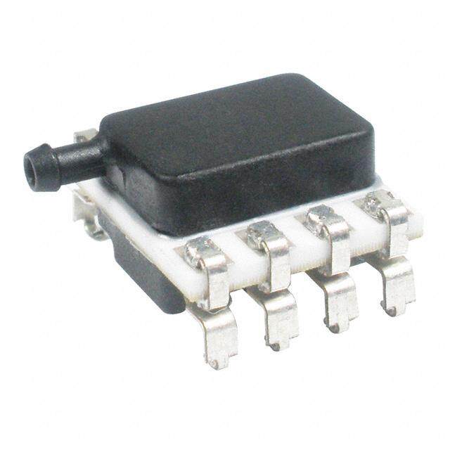
| 描述 | SENSOR ABS PRESS 58PSI MAX板机接口压力传感器 SSOP INTEG W/PORT |
| 产品分类 | |
| 品牌 | Freescale Semiconductor |
| 产品手册 | |
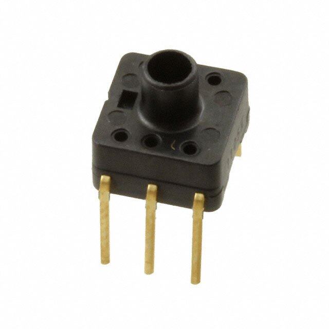
| 产品图片 |
|
| rohs | RoHS 合规性豁免无铅 / 符合限制有害物质指令(RoHS)规范要求 |
| 产品系列 | 板机接口压力传感器,Freescale Semiconductor MPXH6400AC6T1MPXH6400 |
| 数据手册 | |
| 产品型号 | MPXH6400AC6T1 |
| 产品目录绘图 |
|
| 产品目录页面 | |
| 产品种类 | 板机接口压力传感器 |
| 其它名称 | MPXH6400AC6T1CT |
| 准确性 | 1.5 % |
| 出厂设置 | - |
| 单位重量 | 508.200 mg |
| 压力类型 | Absolute |
| 商标 | Freescale Semiconductor |
| 安装风格 | SMD/SMT |
| 封装 | Reel |
| 封装/外壳 | 8-SSOP(0.335",8.50mm 宽),顶部端口 |
| 封装/箱体 | SSOP-8 |
| 工作压力 | 58 psi |
| 工作温度 | -40°C ~ 125°C |
| 工作电源电压 | 5 V |
| 工厂包装数量 | 300 |
| 最大工作温度 | + 125 C |
| 最小工作温度 | - 40 C |
| 标准包装 | 1 |
| 电压-电源 | 4.85 V ~ 5.35 V |
| 电源电压-最大 | 5.36 V |
| 电源电压-最小 | 4.64 V |
| 电源电流 | 6 mA |
| 端口大小 | 0.13 in |
| 端口尺寸 | - |
| 端口类型 | Single Axial Barbless |
| 端子类型 | PCB |
| 精度 | - |
| 系列 | MPXx6400 |
| 输出 | 0 V ~ 4.8 V |
| 输出电压 | 4.8 V |


- 商务部:美国ITC正式对集成电路等产品启动337调查
- 曝三星4nm工艺存在良率问题 高通将骁龙8 Gen1或转产台积电
- 太阳诱电将投资9.5亿元在常州建新厂生产MLCC 预计2023年完工
- 英特尔发布欧洲新工厂建设计划 深化IDM 2.0 战略
- 台积电先进制程称霸业界 有大客户加持明年业绩稳了
- 达到5530亿美元!SIA预计今年全球半导体销售额将创下新高
- 英特尔拟将自动驾驶子公司Mobileye上市 估值或超500亿美元
- 三星加码芯片和SET,合并消费电子和移动部门,撤换高东真等 CEO
- 三星电子宣布重大人事变动 还合并消费电子和移动部门
- 海关总署:前11个月进口集成电路产品价值2.52万亿元 增长14.8%
PDF Datasheet 数据手册内容提取
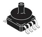
NXP Semiconductors Document Number: MPXH6400A Data Sheet: Technical Data Rev. 6, 03/2017 MPXH6400A, 20 to 400 kPa, Absolute, Integrated Pressure Sensor MPXH6400A The NXP MPXxx6400A series sensor integrates on-chip, bipolar op amp circuitry and thin film resistor networks to provide a high output signal and temperature compensation. The small form factor and high reliability of on-chip integration Super small outline package make this pressure sensor a logical and economical choice for the system designer. The MPXxx6400A series piezoresistive transducer is a state-of-the-art, monolithic, signal conditioned, silicon pressure sensor. This sensor combines advanced micromachining techniques, thin film metallization, and bipolar semiconductor processing to provide an accurate, high level analog output signal that is proportional to applied pressure. MPXHZ6400A6T1 MPXH6400AC6U/6T1/ Features Case 98ARH99066A MPXHZ6400AC6T1 Case 98ARH99089A • Improved accuracy at high temperature • Available in super small outline package • 1.5% maximum error over 0 °C to 85°C Top view • Fully calibrated and compensated • Ideally suited for microprocessor or microcontroller-based systems DNC 5 4 V OUT • Temperature compensated from -40°C to +125°C DNC 6 3 GND • Durable thermoplastic surface mount package DNC 7 2 V S • Package porting and mounting options enable tube attachment for liquefied DNC 8 1 DNC natural gas (LPG) or remote sensing applications Typical applications • Fuel injected car engines Pin 1 identification, chamfered corner. • Vehicles powered by green gases (for example LPG and CNG) Pinout • Small engines • Industrial controls Ordering information # of Ports Pressure type Device Part number Shipping Package None Single Dual Gauge Differential Absolute marking Super Small Outline Package (Media resistant gel) MPXH6400AC6U Rail 98ARH99089A • • MPXH6400A MPXH6400AC6T1 Tape and Reel 98ARH99089A • • MPXH6400A MPXHZ6400A6T1 Tape and Reel 98ARH99066A • • MPXHZ6400A MPXHZ6400AC6T1 Tape and Reel 98ARH99089A • • MPXHZ6400A NXP reserves the right to change the detail specifications as may be required to permit improvements in the design of its products. © NXP B.V. 2017
Contents 1 General Description . . . . . . . . . . . . . . . . . . . . . . . . . . . . . . . . . . . . . . . . . . . . . . . . . . . . . . . . . . . . . . . . . . . . . . . . . . . . . . 3 1.1 Block diagram. . . . . . . . . . . . . . . . . . . . . . . . . . . . . . . . . . . . . . . . . . . . . . . . . . . . . . . . . . . . . . . . . . . . . . . . . . . . . . . 3 1.2 Pinout . . . . . . . . . . . . . . . . . . . . . . . . . . . . . . . . . . . . . . . . . . . . . . . . . . . . . . . . . . . . . . . . . . . . . . . . . . . . . . . . . . . . . 3 2 Mechanical and Electrical Specifications. . . . . . . . . . . . . . . . . . . . . . . . . . . . . . . . . . . . . . . . . . . . . . . . . . . . . . . . . . . . . 4 2.1 Maximum ratings. . . . . . . . . . . . . . . . . . . . . . . . . . . . . . . . . . . . . . . . . . . . . . . . . . . . . . . . . . . . . . . . . . . . . . . . . . . . . 4 2.2 Operating characteristics . . . . . . . . . . . . . . . . . . . . . . . . . . . . . . . . . . . . . . . . . . . . . . . . . . . . . . . . . . . . . . . . . . . . . . 4 3 On-chip Temperature Compensation and Calibration . . . . . . . . . . . . . . . . . . . . . . . . . . . . . . . . . . . . . . . . . . . . . . . . . . 5 4 Package Information. . . . . . . . . . . . . . . . . . . . . . . . . . . . . . . . . . . . . . . . . . . . . . . . . . . . . . . . . . . . . . . . . . . . . . . . . . . . . . 8 4.1 Minimum recommended footprint for surface mounted applications . . . . . . . . . . . . . . . . . . . . . . . . . . . . . . . . . . . . . 8 4.2 Package Dimensions . . . . . . . . . . . . . . . . . . . . . . . . . . . . . . . . . . . . . . . . . . . . . . . . . . . . . . . . . . . . . . . . . . . . . . . . . 9 5 Revision History . . . . . . . . . . . . . . . . . . . . . . . . . . . . . . . . . . . . . . . . . . . . . . . . . . . . . . . . . . . . . . . . . . . . . . . . . . . . . . . . 14 Related Documentation The MPXxx6400A device features and operations are described in a variety of reference manuals, user guides, and application notes. To find the most-current versions of these documents: 1. Go to the MPXx6400 web page at http://www.nxp.com/products/:MPXx6400. 2. Click the Documentation tab. MPXH6400A Sensors 2 NXP B.V.
1 General Description 1.1 Block diagram Figure1 shows a block diagram of the internal circuitry integrated on a pressure sensor chip. V S Thin Film Gain Stage #2 Temperature and ESleenmseinngt Compensation Ground VOUT and Gain Reference Stage #1 Shift Circuitry Pins 1, 5, 6, 7, and 8 are internal device connections. GND Do not connect to external circuitry or ground. Figure1. Integrated pressure sensor block diagram 1.2 Pinout DNC 5 4 V OUT DNC 6 3 GND DNC 7 2 V S DNC 8 1 DNC Pin 1 identification, chamfered corner. Figure2. Device pinout (top view) Table1. Pin functions Pin Name Function 1 DNC Do not connect to external circuitry or ground. Pin 1 is notated by chamfered corner. 2 V Voltage supply S 3 GND Ground 4 V Output voltage OUT 5 DNC Do not connect to external circuitry or ground. 6 DNC Do not connect to external circuitry or ground. 7 DNC Do not connect to external circuitry or ground. 8 DNC Do not connect to external circuitry or ground. MPXH6400A Sensors NXP B.V. 3
2 Mechanical and Electrical Specifications 2.1 Maximum ratings Table2. Maximum ratings(1) Parametrics Symbol Value Units Maximum pressure (P1 > P2) PMAX 1600 kPa Storage temperature TSTG -40° to +125° °C Operating temperature TA -40° to +125° °C Output source current @ full-scale output(2) IO+ 0.5 mAdc Output sink current @ minimum pressure offset(2) IO- -0.5 mAdc 1.Exposure beyond the specified limits may cause permanent damage or degradation to the device. 2.Maximum output current is controlled by effective impedance from V to GND or V to V in the application circuit. OUT OUT S 2.2 Operating characteristics Table3. Operating characteristics (V = 5.0 V , T = 25 °C unless otherwise noted, P1 > P2.) S DC A Characteristic Symbol Min Typ Max Unit Pressure range P 20 — 400 kPa OP Supply voltage(1) V 4.64 5.0 5.36 V S DC Supply current I — 6.0 10 mAdc O Minimum pressure offset(2) (0 to 85°C) @ VS = 5.0 Volts VOFF 0.133 0.2 0.267 VDC Full-scale output(3) (0 to 85°C) @ VS = 5.0 Volts VFSO 4.733 4.8 4.866 VDC Full-scale span(4) (0 to 85°C) @ VS = 5.0 Volts VFSS 4.467 4.6 4.733 VDC Accuracy(5) (0 to 85°C) — — — ±1.5 %V FSS Sensitivity V/P — 12.1 — mV/kPa Response time(6) t — 1.0 — ms R Warm-up time(7) — — 20 — ms Offset stability(8) — — ±0.25 — %V FSS 1.Device is ratiometric within this specified excitation range. 2.Offset (V ) is defined as the output voltage at the minimum rated pressure. OFF 3.Full-scale output (V ) is defined as the output voltage at the maximum or full-rated pressure. FSO 4.Full-scale span (V ) is defined as the algebraic difference between the output voltage at full-rated pressure and the output voltage at the FSS minimum rated pressures 5.Accuracy is the deviation in actual output from nominal output over the entire pressure range and temperature range as a percent of span at 25°C due to all sources of error including the following: Linearity: Output deviation from a straight line relationship with pressure over the specified pressure range. Temperature hysteresis:Output deviation at any temperature within the operating temperature range, after the temperature is cycled to and from the minimum or maximum operating temperature points, with zero differential pressure applied. Pressure hysteresis: Output deviation at any pressure within the specified range, when this pressure is cycled to and from minimum or maximum rated pressure at 25°C TcSpan: Output deviation over the temperature range of 0 to 85°C, relative to 25°C. TcOffset: Output deviation with minimum rated pressure applied, over the temperature range of 0 to 85 °C, relative to 25 °C. Variation from Nominal: The variation from nominal values, for offset or full-scale span, as a percent of V , at 25°C. FSS 6.Response time is defined as the time for the incremental change in the output to go from 10% to 90% of its final value when subjected to a specified step change in pressure. 7.Warm-up time is defined as the time required for the product to meet the specified output voltage after the pressure has been stabilized. 8.Offset stability is the product's output deviation when subjected to 1000 cycles of pulsed pressure, temperature cycling with bias test. MPXH6400A Sensors 4 NXP B.V.
3 On-chip Temperature Compensation and Calibration Figure3 illustrates the absolute sensing chip in the basic super small outline chip carrier (case 98ARH99066A). Figure4 shows a typical application circuit (output source current operation). Figure5 shows the sensor output signal relative to pressure input. Typical minimum and maximum output curves are shown for operation over 0 to 85°C temperature range. The output will saturate outside of the rated pressure range. A fluorosilicone gel isolates the die surface and wire bonds from the environment, while allowing the pressure signal to be transmitted to the silicon diaphragm. The MPXH6400A/MPXHZ6400A pressure sensor operating characteristics, internal reliability and qualification tests are based on use of dry air as the pressure media. Media other than dry air may have adverse effects on sensor performance and long-term reliability. Contact the factory for information regarding media compatibility in your application. Fluorosilicone Die Gel Die Coat Stainless Steel Cap P1 Thermoplastic Wire Case Bond Lead Frame Absolute Sealed Vacuum Die Bond Reference Figure3. Cross-sectional diagram (not-to-scale) +5.1 V V S VOUT To ADC 100 nF 1 μF GND 47 pF 51 K Figure4. Recommended power supply decoupling and output filtering MPXH6400A Sensors NXP B.V. 5
5.0 Transfer Function: 4.5 V = V x (0.002421xP–0.00842 ± Error OUT S 4.0 VS = 5.0 VDC Temperature = 0 to 85°C 3.5 s) 3.0 Volt MAX ut ( 2.5 p ut 2.0 O TYP 1.5 1.0 0.5 MIN 0 00000000000000000000 24680246802468024680 1111122222333334 Pressure (Reference to Sealed Vacuum) in kPa Figure5. Output vs. absolute pressure Normal Transfer Value: V = V x (0.002421 x P – 0.00842) OUT S ± Pressure Error x Temp. Factor x 0.002421 x V S V = 5.0 ± 0.36 V S DC Figure6. Transfer function 4.0 or ct Fa 3.0 or Err e 2.0 Break Points ur at er p m 1.0 e T Temp Multiplier 0.0 -40 -20 0 20 40 60 80 100 120 140 - 40 3 Temperature in °C 0 to 85 1 125 1.75 NOTE: The Temperature Multiplier is a linear response from 0°C to -40°C and from 85°C to 125°C Figure7. Temperature error band MPXH6400A Sensors 6 NXP B.V.
Error Limits for Pressure 6.0 ±5.5 (kPa) 5.0 4.0 3.0 a) 2.0 P or (k 1.0 Err 0.0 e 20 40 60 80 100120140160 180200220 240260280300320340 360380400 sur -1.0 s e Pr -2.0 -3.0 -4.0 - 5.0 Pressure (in kPa) - 6.0 Pressure Error (Max) 20 to 400 (kPa) ±5.5 (kPa) Figure8. Pressure error band MPXH6400A Sensors NXP B.V. 7
4 Package Information 4.1 Minimum recommended footprint for surface mounted applications Surface mount board layout is a critical portion of the total design. The footprint for the semiconductor package must be the correct size to ensure proper solder connection interface between the board and the package. With the correct pad geometry, the packages will self-align when subjected to a solder reflow process. It is always recommended to fabricate boards with a solder mask layer to avoid bridging and/or shorting between solder pads, especially on tight tolerances and/or tight layouts. 0.050 0.387 1.27 9.83 TYP 0.150 3.81 0.027 TYP 8X 0.69 0.053 TYP 8X inch 1.35 mm Figure9. SSOP footprint MPXH6400A Sensors 8 NXP B.V.
4.2 Package Dimensions This drawing is located at http://cache.nxp.com/assets/documents/data/en/package-information/98ARH99066A.pdf. Case 98ARH99066A, super small outline package, surface mount MPXH6400A Sensors NXP B.V. 9
Case 98ARH99066A, super small outline package, surface mount MPXH6400A Sensors 10 NXP B.V.
Case 98ARH99066A, super small outline package, surface mount MPXH6400A Sensors NXP B.V. 11
This drawing is located at http://cache.nxp.com/assets/documents/data/en/package-information/98ARH99089A.pdf. Case 98ARH99089A, small outline package, surface mount MPXH6400A Sensors 12 NXP B.V.
Case 98ARH99089A, small outline package, surface mount MPXH6400A Sensors NXP B.V. 13
5 Revision History Table4. Revision history Document ID Release Date Data sheet status Change notice Supersedes MPXH6400A Rev. 6 2017 March Technical data — MPXH6400A Rev. 5.0 • Revised V = 10.0 V value to V = 5.0 V inTable3. S DC S DC • The format of this data sheet has been redesigned to comply with current identity guidelines of NXP Modifications Semiconductors. Legal texts have been adapted to the new company name where appropriate. • Updated package outlines Section4.2, “Package Dimensions” to comply with current identity guidelines of NXP Semiconductors. MPXH6400A Rev. 5.0 2015 September Technical data — MPXH64-00A Rev. MPXH6400A Sensors 14 NXP B.V.
How to Reach Us: Information in this document is provided solely to enable system and software implementers to use NXP products. There are no expressed or implied copyright Home Page: NXP.com licenses granted hereunder to design or fabricate any integrated circuits based on the Web Support: information in this document. NXP reserves the right to make changes without further http://www.nxp.com/support notice to any products herein. NXP makes no warranty, representation, or guarantee regarding the suitability of its products for any particular purpose, nor does NXP assume any liability arising out of the application or use of any product or circuit, and specifically disclaims any and all liability, including without limitation, consequential or incidental damages. "Typical" parameters that may be provided in NXP data sheets and/or specifications can and do vary in different applications, and actual performance may vary over time. All operating parameters, including "typicals," must be validated for each customer application by the customer's technical experts. NXP does not convey any license under its patent rights nor the rights of others. NXP sells products pursuant to standard terms and conditions of sale, which can be found at the following address: http://www.nxp.com/terms-of-use.html. NXP, the NXP logo, Freescale, the Freescale logo, and the Energy Efficient Solutions logo are trademarks of NXP B.V. All other product or service names are the property of their respective owners. All rights reserved. © NXP B.V. 2017. Document Number: MPXH6400A Rev. 6 03/2017
Mouser Electronics Authorized Distributor Click to View Pricing, Inventory, Delivery & Lifecycle Information: N XP: MPXHZ6400A6T1 MPXHZ6400AC6T1 MPXH6400AC6U MPXH6400AC6T1