ICGOO在线商城 > 集成电路(IC) > 接口 - 传感器,电容式触摸 > MPR031EPR2
 Datasheet下载
- 型号: MPR031EPR2
- 制造商: Freescale Semiconductor
- 库位|库存: xxxx|xxxx
- 要求:
| 数量阶梯 | 香港交货 | 国内含税 |
| +xxxx | $xxxx | ¥xxxx |
查看当月历史价格
查看今年历史价格
MPR031EPR2产品简介:
ICGOO电子元器件商城为您提供MPR031EPR2由Freescale Semiconductor设计生产,在icgoo商城现货销售,并且可以通过原厂、代理商等渠道进行代购。 MPR031EPR2价格参考。Freescale SemiconductorMPR031EPR2封装/规格:接口 - 传感器,电容式触摸, Capacitive Touch Buttons 8-QFN-D (2x2)。您可以下载MPR031EPR2参考资料、Datasheet数据手册功能说明书,资料中有MPR031EPR2 详细功能的应用电路图电压和使用方法及教程。
NXP USA Inc. 的 MPR031EPR2 是一款电容式触摸传感器接口芯片,属于接口 - 传感器分类。该型号主要应用于需要高性能、低功耗和高灵敏度的电容式触摸解决方案的场景。以下是其主要应用场景:

 1. 消费电子设备
   - 家用电器:如冰箱、洗衣机、微波炉等家电产品中,用于替代传统的机械按键,提供更现代化的触控界面。
   - 遥控器:在电视或多媒体设备的遥控器上,实现滑动、点击等操作,提升用户体验。
   - 音频设备:音响、耳机充电盒等设备中,用于音量调节、播放/暂停等功能。

 2. 智能家居
   - 智能开关:用于墙壁开关、灯光控制面板等,通过触摸实现开关灯或调节亮度。
   - 智能门锁:作为门锁上的触摸传感器,检测用户的手指输入以触发密码输入或解锁功能。
   - 环境监测设备:如温湿度传感器、空气质量监测仪等,提供触摸式菜单选择或参数调整。

 3. 工业控制
   - 人机交互界面 (HMI):在工业设备的操作面板上,用作按钮、滑块或滚轮的触摸控制。
   - 仪器仪表:用于实验室或工业现场的仪器设备,提供直观的触摸操作方式。

 4. 医疗设备
   - 便携式医疗设备:如血糖仪、血压计等,通过触摸屏实现简单的功能切换或数据查看。
   - 监护设备:如心率监测仪,利用电容式触摸传感器检测用户的手指接触并启动测量功能。

 5. 汽车电子
   - 车内控制面板:用于空调控制、座椅调节、娱乐系统等触摸界面。
   - 车门把手:检测用户接近或触摸动作,自动触发车门解锁或照明功能。

 6. 可穿戴设备
   - 智能手表/手环:用于触摸屏或侧边按钮的替代,实现便捷操作。
   - 健康监测设备:如皮肤接触式传感器,检测用户的生理信号。

MPR031EPR2 支持多点触摸检测,具备抗噪能力强、响应速度快的特点,适合在复杂电磁环境中使用。此外,它还支持防水设计,能够在潮湿环境下正常工作,进一步拓宽了其应用范围。
| 参数 | 数值 |
| 产品目录 | |
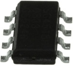
| 描述 | IC CTLR TOUCH SENSOR 8-DFN电容触摸传感器 PESCE DFN |
| 产品分类 | 电容式触摸传感器,接近传感器 IC电容触摸传感器 |
| 品牌 | Freescale Semiconductor |
| 产品手册 | |
| 产品图片 |
|
| rohs | 符合RoHS无铅 / 符合限制有害物质指令(RoHS)规范要求 |
| 产品系列 | Freescale Semiconductor MPR031EPR2- |
| 数据手册 | |
| 产品型号 | MPR031EPR2 |
| 产品培训模块 | http://www.digikey.cn/PTM/IndividualPTM.page?site=cn&lang=zhs&ptm=16851 |
| 产品目录页面 | |
| 产品种类 | 电容触摸传感器 |
| 供应商器件封装 | 8-QFN-D(2x2) |
| 其它名称 | MPR031EPR2DKR |
| 分辨率(位) | - |
| 包装 | Digi-Reel® |
| 单位重量 | 6 mg |
| 参考设计库 | http://designs.digikey.com/library/4294959886/4294959868/595 |
| 商标 | Freescale Semiconductor |
| 安装类型 | 表面贴装 |
| 封装 | Reel |
| 封装/外壳 | 8-UFDFN |
| 封装/箱体 | UDFN-8 |
| 尺寸 | 2 mm L x 2 mm W x 0.6 (Max) mm H |
| 工作温度 | -40°C ~ 85°C |
| 工厂包装数量 | 3000 |
| 数据接口 | I²C |
| 数据速率/采样率(SPS,BPS) | 400k |
| 标准包装 | 1 |
| 特色产品 | http://www.digikey.com/cn/zh/ph/Freescale/MPR03x.html |
| 电压-电源 | 1.71 V ~ 2.75 V |
| 电压基准 | - |
| 电流-电源 | 43µA |
| 电源电压 | 1.8 V |
| 类型 | 电容性 |
| 系列 | MPR03x |
| 触摸面板接口 | 2 线 |
| 评估工具 | 可供 |
| 输入/按键数 | - |
| 配用 | /product-detail/zh/KITMPR03XEVM/KITMPR03XEVM-ND/2063066/product-detail/zh/DEMOMPR031/DEMOMPR031-ND/2063063 |


- 商务部:美国ITC正式对集成电路等产品启动337调查
- 曝三星4nm工艺存在良率问题 高通将骁龙8 Gen1或转产台积电
- 太阳诱电将投资9.5亿元在常州建新厂生产MLCC 预计2023年完工
- 英特尔发布欧洲新工厂建设计划 深化IDM 2.0 战略
- 台积电先进制程称霸业界 有大客户加持明年业绩稳了
- 达到5530亿美元!SIA预计今年全球半导体销售额将创下新高
- 英特尔拟将自动驾驶子公司Mobileye上市 估值或超500亿美元
- 三星加码芯片和SET,合并消费电子和移动部门,撤换高东真等 CEO
- 三星电子宣布重大人事变动 还合并消费电子和移动部门
- 海关总署:前11个月进口集成电路产品价值2.52万亿元 增长14.8%


PDF Datasheet 数据手册内容提取
Freescale Semiconductor MPR03X Data Sheet: Technical Data Rev 7, 7/2012 An Energy Efficient Solution by Freescale Proximity Capacitive Touch MPR031 Sensor Controller MPR032 The MPR03X is an Inter-Integrated Circuit Communication (I2C) driven Capacitive Touch Sensor Controller, optimized to manage two electrodes with interrupt functionality, or three electrodes with the Bottom View interrupt disabled. It can accommodate a wide range of implementations due to increased sensitivity and a specialized feature set. Features • 6 µA supply current with two electrodes being monitored with 8-PIN DFN 32ms response time and IRQ enabled CASE 1944 • Compact 2 x 2 x 0.65 mm 8-lead µDFN package • Supports up to 3 touch pads Top View • Only one external component needed • Intelligent touch detection capacity SCL 1 8 IRQ/ELE2 • 4 µA maximum shutdown current • 1.71 V to 2.75 V operation SDA 2 7 ELE1 MPR03X • Threshold based detection with hysteresis • I2C interface, with optional IRQ VSS 3 6 ELE0 • Multiple devices in a system allow for up to 6 electrodes (need MPR032 with second I2C address) VDD 4 5 REXT • -40°C to +85°C operating temperature range Figure1. Pin Connections Implementations • Switch Replacements VDD • Touch Pads Typical Applications I²CSerial SCL • PC Peripherals Interface SDA ELE0 1 • MP3 Players MPR03X INT • Remote Controls ELE1 2 REXT • Mobile Phones • Lighting Controls 75k VSS VSS MPR03X with 2 Electrodes and 2 Pads ORDERING INFORMATION Device Name Temperature Range Case Number Touch Pads I2C Address Shipping MPR031EPR2 -40C to +85C 1944 (8-Pin DFN) 3-pads 0x4A Tape and Reel MPR032EPR2 -40C to +85C 1944 (8-Pin DFN) 3-pads 0x4B Tape and Reel © 2008, 2009, 2011, 2012 Freescale Semiconductor, Inc. All rights reserved.
1 Device Overview 1.1 Introduction MPR03X is a small outline, low profile, low voltage touch sensor controller in a 2 mm x 2 mm DFN which manages up to three touch pad electrodes. An I2C interface communicates with the host controller at data rates up to 400 kbits/sec. An optional interrupt output advises the host of electrode status changes. The interrupt output is a multiplexed with the third electrode output, so using the interrupt output reduces the number of electrode inputs to two. The MPR03X includes three levels of input signal filtering to detect pad input condition changes due to touch without any processing by the application. 1.2 Internal Block Diagram Debounce 32kHz 8MHz 8MHz SDA SDA I²C Interval Oscillator Oscillator SCL SCL Interface Debounce Debounce Shutdown Shutdown Traffic Count and User Sample Sample Registers Interval Counters 32kHz8MHz CLR Sample Shutdown Interrupt Count ADCController StartConversion Controller Numberof Electrodes IRQ IRQ SET SetInputChannel SetGrounded Electrodes Un-Touched SetSourceCurrent Baseline Filter Debounced Average DebounceFilterRegisters Average SampleFilterRegisters Results Filtered 4xMaxRegisters Filtered MaxRegister ADCResult Magnitude Debounce 4xSumRegisters Sample SumRegister Result Comparator Result 4xMinRegisters MinRegister Iset SetSourceCurrent Mirror 3 REXT 0V CurrentSourceMultiplexor SelectChan SetInputChannel 2 0 1 2 ELE0 0 SCehleacnt 2 ELE1 1 Inpu CEonnavbelert SSthaurttCdoownvnersion t 10BitADC ELE2 2 S Clock 8MHz o urc Data 10 ADCResult e M u ltip le x Iref or Sel SetGrounded 4 Electrodes Figure2. Functional Block Diagram MPR03X Sensors 2 Freescale Semiconductor
2 External Signal Description 2.1 Device Pin Assignment Table1 shows the pin assignment for the MPR03X. For a more detailed description of the functionality of each pin, refer to the appropriate chapter. Table1. Device Pin Assignment Pin Name Function 1 SCL I2C Serial Clock Input 2 SDA I2C Serial Data I/O 3 V Ground SS 4 V Positive Supply Voltage DD 5 REXT Reference Resistor Connect a 75 k ±1% resistor from REXT to V SS 6 ELE0 Electrode 0 7 ELE1 Electrode 1 8 IRQ/ELE2 Interrupt Output or Touch Electrode Input 2 IRQ is the active-low open-drain interrupt output The package available for the MPR03X is a 2 x 2 mm 8 pin DFN. The package and pinout is shown in Figure3. SCL 1 8 IRQ/ELE2 SDA 2 7 ELE1 MPR03X VSS 3 6 ELE0 VDD 4 5 REXT Figure3. Package Pinouts 2.2 Recommended System Connections The MPR03X Capacitive Touch Sensor Controller requires one external passive component. As shown in Table1, the REXT line should have a 75 kconnected from the pin to GND. This resistor needs to be 1% tolerance. In addition to the one resistor, a bypass capacitor of 10 µF should always be used between the V and V lines and a DD SS 4.7 k pull-up resistor should be included on the IRQ. Note: This condition is when pin 8 is used for interrupt indication and not for electrode sensing. The remaining two connections are SCL and SDA. Depending on the specific application, each of these control lines can be used by connecting them to a host controller. In the most minimal system, the SCL and SDA must be connected to a master I2C interface to communicate with the MPR03X. All of the connections for the MPR03X are shown by the schematic in Figure4. VDD I²CSerial SCL ELE0 1 Interface SDA MPR03X ELE1 2 REXT 75k IRQ/ELE2 3 VSS VSS MPR03X Sensors Freescale Semiconductor 3
Figure4. Recommended System Connections Schematic 2.3 Serial Interface The MPR03X uses an I2C Serial Interface. The I2C protocol implementation and the specifics of communicating with the Touch Sensor Controller are detailed in the following sections. 2.3.1 Serial-Addressing The MPR03X operates as a slave that sends and receives data through an I2C 2-wire interface. The interface uses a Serial Data Line (SDA) and a Serial Clock Line (SCL) to achieve bi-directional communication between master(s) and slave(s). A master (typically a microcontroller) initiates all data transfers to and from the MPR03X, and it generates the SCL clock that synchronizes the data transfer. The MPR03X SDA line operates as both an input and an open-drain output. A pull-up resistor, typically 4.7k, is required on SDA. The MPR03X SCL line operates only as an input. A pull-up resistor, typically 4.7k, is required on SCL if there are multiple masters on the 2-wire interface, or if the master in a single-master system has an open-drain SCL output. Each transmission consists of a START condition (Figure5) sent by a master, followed by the MPR03X’s 7-bit slave address plus R/W bit, a register address byte, one or more data bytes, and finally a STOP condition. SDA t BUF t t SUDAT SUSTA t tHDDAT HDSTA tSUSTO t LOW SCL t HIGH t HDSTA t t R F START REPEATEDSTART STOP START CONDITION CONDITION CONDITION CONDITION Figure5. Wire Serial Interface Timing Details 2.3.2 Start and Stop Conditions Both SCL and SDA remain high when the interface is not busy. A master signals the beginning of a transmission with a START (S) condition by transitioning SDA from high to low while SCL is high. When the master has finished communicating with the slave, it issues a STOP (P) condition by transitioning SDA from low to high while SCL is high. The bus is then free for another transmission. SDA SCL DATALINESTABLE DATAVALID CHANGEOF DATAALLOWED Figure6. Bit Transfer MPR03X Sensors 4 Freescale Semiconductor
2.3.3 Bit Transfer One data bit is transferred during each clock pulse (Figure7). The data on SDA must remain stable while SCL is high. SDA SCL S P START STOP CONDITION CONDITION Figure7. Stop and Start Conditions 2.3.4 Acknowledge The acknowledge bit is a clocked 9th bit (Figure8) which the recipient uses to handshake receipt of each byte of data. Thus each byte transferred effectively requires 9 bits. The master generates the 9th clock pulse, and the recipient pulls down SDA during the acknowledge clock pulse, such that the SDA line is stable low during the high period of the clock pulse. When the master is transmitting to the MPR03X, the MPR03X generates the acknowledge bit, since the MPR03X is the recipient. When the MPR03X is transmitting to the master, the master generates the acknowledge bit, since the master is the recipient. START CLOCKPULSEFOR CONDITION ACKNOWLEDGEMENT SCL 1 2 8 9 SDA BYTRANSMITTER S SDA BYRECEIVER Figure8. Acknowledge 2.3.5 The Slave Address The MPR03X has a 7-bit long slave address (Figure9). The bit following the 7-bit slave address (bit eight) is the R/W bit, which is low for a write command and high for a read command. SDA 1 0 0 1 0 1 0 R/W ACK MSB SCL Figure9. Slave Address The MPR03X monitors the bus continuously, waiting for a START condition followed by its slave address. When a MPR03X recognizes its slave address, it acknowledges and is then ready for continued communication. The MPR031 and MPR032 slave addresses are show in Table2. Table2. Part Number I2C Address MPR031 0x4A MPR032 0x4B MPR03X Sensors Freescale Semiconductor 5
2.3.6 Message Format for Writing the MPR03X A write to the MPR03X comprises the transmission of the MPR03X’s keyscan slave address with the R/W bit set to 0, followed by at least one byte of information. The first byte of information is the command byte. The command byte determines which register of the MPR03X is to be written by the next byte, if received. If a STOP condition is detected after the command byte is received, the MPR03X takes no further action (Figure10) beyond storing the command byte. Any bytes received after the command byte are data bytes. CommandbyteisstoredonreceiptofSTOPcondition D15 D14 D13 D12 D11 D10 D9 D8 acknowledgefromMPR03X S SLAVEADDRESS 0 A COMMANDBYTE A P R/W acknowledgefromMPR3X Figure10. Command Byte Received Any bytes received after the command byte are data bytes. The first data byte goes into the internal register of the MPR03X selected by the command byte (Figure11). acknowledgefrom acknowledgefrom MPR03X MPR03X Howcommandbyteanddatabyte mapintoMPR03X'sregisters D15 D14 D13 D12 D11 D10 D9 D8 D7 D6 D5 D4 D3 D2 D1 D0 acknowledgefromMPR03X S SLAVEADDRESS 0 A COMMANDBYTE A DATABYTE A P 1byte R/W auto-incrementmemory wordaddress Figure11. Command and Single Data Byte Received If multiple data bytes are transmitted before a STOP condition is detected, these bytes are generally stored in subsequent MPR03X internal registers because the command byte address generally auto-increments (Section2.4). 2.3.7 Message Format for Reading the MPR03X MPR03X is read using MPR03X's internally stored register address as address pointer, the same way the stored register address is used as address pointer for a write. The pointer generally auto-increments after each data byte is read using the same rules as for a write (Table5). Thus, a read is initiated by first configuring MPR03X's register address by performing a write (Figure10) followed by a repeated start. The master can now read 'n' consecutive bytes from MPR03X, with first data byte being read from the register addressed by the initialized register address. acknowledgefrommaster D7 D6 D5 D4 D3 D2 D1 D0 acknowledgefromMPR03X S SLAVEADDRESS 1 A DATABYTE NAA P nbytes R/W auto-incrementmemory wordaddress Figure12. Reading MPR03X MPR03X Sensors 6 Freescale Semiconductor
2.3.8 Operation with Multiple Master The application should use repeated starts to address the MPR03X to avoid bus confusion between I2C masters.On a I2C bus, once a master issues a start/repeated start condition, that master owns the bus until a stop condition occurs. If a master that does not own the bus attempts to take control of that bus, then improper addressing may occur. An address may always be rewritten to fix this problem. Follow I2C protocol for multiple master configurations. 2.4 Register Address Map Table3. Register Address Map Burst Mode Register Register Address Auto-Increment Address Touch Status Register 0x00 ELE0 Filtered Data Low Register 0x02 ELE0 Filtered Data High Register 0x03 ELE1 Filtered Data Low Register 0x04 ELE1 Filtered Data High Register 0x05 ELE2 Filtered Data Low Register 0x06 ELE2 Filtered Data High Register 0x07 ELE0 Baseline Value Register 0x1A ELE1 Baseline Value Register 0x1B ELE2 Baseline Value Register 0x1C Max Half Delta Register 0x26 Register Address + 1 Noise Half Delta Register 0x27 Noise Count Limit Register 0x28 ELE0 Touch Threshold Register 0x29 ELE0 Release Threshold Register 0x2A ELE1 Touch Threshold Register 0x2B ELE1 Release Threshold Register 0x2C ELE2 Touch Threshold Register 0x2D ELE2 Release Threshold Register 0x2E AFE Configuration Register 0x41 Filter Configuration Register 0x43 Electrode Configuration Register 0x44 0x00 MPR03X Sensors Freescale Semiconductor 7
3 Functional Overview 3.1 Introduction The MPR03X has an analog front, a digital filter, and a touch recognition system. This data interpretation can be done many different ways but the method used in the MPR03X is explained in this chapter. 3.2 Understanding the Basics MPR03X is a touch pad controller which manages two or three touch pad electrodes. An I²C interface communicates with the host, and an optional interrupt output advises the host of electrode status changes. The interrupt output is a multiplexed function with the third electrode input, so using the interrupt output reduces the number of electrode inputs to two. The primary application for MPR03X is the management of user interface touch pads. Monitoring touch pads involves detecting small changes of pad capacitance. MPR03X incorporates a self calibration function which continually adjusts the baseline capacitance for each individual electrode. Therefore, the host only has to configure the delta thresholds to interpret a touch or release. MPR03X uses a state machine to operate a capacitive measurement engine to analyze the electrodes and determine whether a pad has been touched or released. Between measurements the MPR03X draws negligible current. The application controls MPR03X's configuration, making trade-offs between noise rejection, touch response time, and power consumption. 3.3 Implementation The touch sensor system can be tailored to specific applications by varying the following: a capacitance detector, a raw data low pass filter, a baseline management system, and a touch detection system. In the following sections, the functionality and configuration of each block will be described. Electrodes can be connected to the MPR03X in two different configurations, one with an IRQ and one without (Figure13). VDD VDD ELE0 1 I²CSerial SCL I²CSerial SCL Interface ELE0 1 Interface SDA SDA MPR03X MPR03X ELE1 2 INT REXT ELE1 2 REXT ELE2 3 75k 75k VSS VSS VSS VSS MPR03X with 2 Electrodes and 2 Pads MPR03X with 3 Electrodes and 3 Pads Figure13. MPR03X Pad and Interrupt Connection Options MPR03X Sensors 8 Freescale Semiconductor
4 Modes of Operation 4.1 Introduction MPR03X’s operation modes are Stop, Run1, and Run2. Stop mode is the start-up and configuration mode. 4.2 Stop Mode In Stop mode, the MPR03X does not monitor any of the electrodes. This mode is the lowest power state. 4.2.1 Initial Power Up On power-up, the device is in Stop mode, registers are reset to the initial values shown in Table4, and MPR03X starts in Stop mode drawing minimal supply current. The user configurable pin IRQ/ELE2 defaults to being the interrupt output IRQ function. IRQ is reset on power-up, and so defaults to logic high. Since the IRQ is an open-drain output, IRQ will be high impedance. Table4. Power-Up Register Configurations Register Power-Up Condition Register Address HEX Value Touch Status Register Cleared 0x00 0x00 ELE0 Filtered Data Low Register Cleared 0x02 0x00 ELE0 Filtered Data High Register Cleared 0x03 0x00 ELE1 Filtered Data Low Register Cleared 0x04 0x00 ELE1 Filtered Data High Register Cleared 0x05 0x00 ELE2 Filtered Data Low Register Cleared 0x06 0x00 ELE2 Filtered Data High Register Cleared 0x07 0x00 ELE0 Baseline Value Register Cleared 0x1A 0x00 ELE1 Baseline Value Register Cleared 0x1B 0x00 ELE2 Baseline Value Register Cleared 0x1C 0x00 Max Half Delta Register Cleared 0x26 0x00 Noise Half Delta Register Cleared 0x27 0x00 Noise Count Limit Register Cleared 0x28 0x00 ELE0 Touch Threshold Register Cleared 0x29 0x00 ELE0 Release Threshold Register Cleared 0x2A 0x00 ELE1 Touch Threshold Register Cleared 0x2B 0x00 ELE1 Release Threshold Register Cleared 0x2C 0x00 ELE2 Touch Threshold Register Cleared 0x2D 0x00 ELE2 Release Threshold Register Cleared 0x2E 0x00 AFE Configuration Register 6 AFE samples, 16 µA charge current 0x41 0x10 Filter Configuration Register 16 ms detection sample interval, 0x43 0x24 4 samples for the second level filter, 0.5 µS charge time Electrode Configuration Register Stop mode. ELE2/IRQ pin is interrupt 0x44 0x00 function, 4.2.2 Stop Mode Usage In order to set the configuration registers, the device must be in stop mode. This is achieved by setting the EleEn field in the Electrode Configuration register to zero. MPR03X Sensors Freescale Semiconductor 9
4.3 Run1 Mode In Run1 Mode, the MPR03X monitors 1, 2, or 3 electrodes which are connected to a user defined array of touch pads. When only 1 or 2 electrodes are selected, the IRQ/ELE2 pin is automatically configured as an open drain interrupt output. When 3 electrodes are selected in Run1 Mode, the IRQ/ELE2 pin becomes the third electrode input, ELE2 (Figure14). Run1Modewith3Electrodes Run1Modewith2Electrodes ELE0 ELE0 1 1 Capacitance ELE1 Capacitance Filters ELE1 Measurement Filters 2 Measurement and 2 Engine and Engine Touch Touch 3 ELE2 Detection INT Interrupt Detection Run1Modewith1Electrode ELE0 Capacitance 1 Measurement Filters Engine and Touch Detection INT Interrupt Figure14. Electrode/Pad Connections in Run Mode 4.4 Run2 Mode In Run2 Mode, all enabled electrodes act as a single electrode by internally connecting the electrode pins together. The entire surface of all the touch pads is used as a single pad, increasing the total area of the conductor. When 2 electrodes are selected in Run2 Mode, the IRQ/ELE2 pin is automatically configured as an open drain interrupt output. When 3 electrodes are selected, the IRQ/ELE2 pin becomes the third electrode input, ELE2 (Figure15). Run2Modeto3Pads Run2Modeto2Pads ELE0 ELE0 1 1 Capacitance ELE1 Capacitance Filters ELE1 Measurement Filters 2 Measurement and 2 Engine and Engine Touch Touch ELE2 3 Detection INT Interrupt Detection Figure15. Electrode/Pad Connections in Area Detection Mode 4.5 Electrode Configuration Register The Electrode Configuration Register manages the configuration of the Electrode outputs in addition to the mode of the part. The address of the Electrode Configuration Register is 0x44. 7 6 5 4 3 2 1 0 R 0 CalLock ModeSel EleEn W Reset: 0 0 0 0 0 0 0 0 = Unimplemented Figure16. Electrode Configuration Register MPR03X Sensors 10 Freescale Semiconductor
Table5. Electrode Configuration Register Field Descriptions Field Description 6 Calibration Lock – The Calibration Lock bit selects whether calibration is enabled CalLock or disabled. 0 Enabled – In this state baseline calibration is enabled. 1 Disabled – In this state baseline calibration is disabled. 5:4 Mode Select – The Mode Select field selects which Run Mode the sensor will ModeSel operate in. This register is ignored when in Stop Mode. 00 Encoding 0 – Run1 Mode is enabled. 01 Encoding 1 – Run2 Mode is enabled. 10 Encoding 2 – Run2 Mode is enabled. 11 Encoding 3 – Run2 Mode is enabled. 3:0 Electrode Enable – The Electrode Enable Field selects the electrode and IRQ EleEn functionality. 0000 Encoding 0 – Stop Mode 0001 Encoding 1 – Run Mode with ELE0 is enabled, ELE1 is disabled, IRQ is enabled. 0010 Encoding 2 – Run Mode with ELE0 is enabled, ELE1 is enabled, IRQ is enabled. 0011 Encoding 3 – Run Mode with ELE0 is enabled, ELE1 is enabled, ELE2 is enabled. ~ 1111 Encoding 15 – Run Mode with ELE0 is enabled, ELE1 is enabled, ELE2 is enabled. MPR03X Sensors Freescale Semiconductor 11
5 Output Mechanisms 5.1 Introduction The MPR03X has three outputs: the touch status, values from the second level filter (Section8.3), and the calibrated baseline values. The application can either use the touch status or a combination of second level filter data with the baseline data to determine when a touch occurs. 5.2 Touch Status Each Electrode has an associated single bit that denotes whether or not the pad is currently touched. This output is generated using the touch threshold and release threshold registers to determine when a pad is considered touched or untouched. Configuration of this system is discussed in Section9. 5.2.1 Touch Status Register The Touch Pad Status Register is a read only register for determining the current status of the touch pad. The I2C slave address of the Touch Pad Status Register is 0x00. 7 6 5 4 3 2 1 0 R 0 0 0 0 E2S E1S E0S OCF W Reset: 0 0 0 0 0 0 0 0 = Unimplemented Figure17. Touch Status Register Table6. Touch Pad Status Register Field Descriptions Field Description 7 Over Current Flag – The Over Current Flag shows when too much current is on the REXT OCF pin. If it is set all other status flags and registers are cleared and the device is set to Stop mode. When OCF is set, the MPR03X cannot be put back into a Run mode. 0 – Current is within limits. 1 – Current is above limits. Writing a 1 to this field will clear the OCF. 2 Electrode 2 Status – The Electrode 2 Status bit shows touched or not touched. E2S 0 – Not Touched 1 – Touched 1 Electrode 1 Status – The Electrode 1 Status bit shows touched or not touched. E1S 0 – Not Touched 1 – Touched 0 Electrode 0 Status – The Electrode 0 Status bit shows touched or not touched. E0S 0 – Not Touched 1 – Touched MPR03X Sensors 12 Freescale Semiconductor
5.3 Filtered Data Each electrode has an associated filtered output. This output is generated through register settings and a low pass filter implementation (Section8.4). 5.3.1 Filtered Data Low Register The Filtered Data Low register contains the data on each of the electrodes. It is paired with the Filtered Data High register for reading the 10 bit A/D value. The address of the ELE0 Filtered Data Low register is 0x02. The address of the ELE1 Filtered Data Low register is 0x04. The address of the ELE2 Filtered Data Low register is 0x06. 7 6 5 4 3 2 1 0 R FDLB W Reset: 0 0 0 0 0 0 0 0 = Unimplemented Figure18. Filtered Data Low Register Table7. Filtered Data Low Register Field Descriptions Field Description 7:0 Filtered Data Low Byte – The Filtered Data Low Byte displays the lower 8 bits of FDLB the 10 bit filtered A/D reading. 00000000 Encoding 0 ~ 11111111 Encoding 255 5.3.2 Filtered Data High Register The Filtered Data High register contains the data on each of the electrodes. It is paired with the Filtered Data Low register for reading the 10 bit A/D value. The address of the ELE0 Filtered Data High register is 0x03. The address of the ELE1 Filtered Data High register is 0x05. The address of the ELE2 Filtered Data High register is 0x07. 7 6 5 4 3 2 1 0 R 0 0 0 0 0 0 FDHB W Reset: 0 0 0 0 0 0 0 0 = Unimplemented Figure19. Filtered Data High Register Table8. Filtered Data High Register Field Descriptions Field Description 7:0 Filtered Data High Bits – The Filtered Data High Bits displays the higher 2 bits of FDHB the 10 bit filtered A/D reading. 00 Encoding 0 ~ 11 Encoding 3 MPR03X Sensors Freescale Semiconductor 13
5.4 Baseline Values In addition to the second level filter data, the data from the baseline filter (or third level filter) is also displayed. In this case, the least two significant bits are removed before the 10-bit value is displayed in the register. 5.4.1 Baseline Value Register The Baseline Value register contains the third level filtered data on each of the electrodes. It is a truncated 10 bit A/D value displayed in the 8 bit register. The address of the ELE0 Baseline Value register is 0x1A. The address of the ELE1 Baseline Value register is 0x1B. The address of the ELE2 Baseline Value register is 0x1C. 7 6 5 4 3 2 1 0 R BV W Reset: 0 0 0 0 0 0 0 0 = Unimplemented Figure20. Filtered Data High Register Table9. Filtered Data High Register Field Descriptions Field Description 7:0 Baseline Value – The Baseline Value byte displays the higher 8 bits of the 10 bit BV baseline value. 00000000 Encoding 0 – The 10 bit baseline value is between 0 and 3. ~ 11111111 Encoding 255 – The 10 bit baseline value is between 1020 and 1023. MPR03X Sensors 14 Freescale Semiconductor
6 Interrupts 6.1 Introduction The MPR03X has one interrupt output that is triggered on any touch related event. The interrupts trigger on both the up or down motion of a finger as defined by a set of configurable thresholds. 6.2 Triggering an Interrupt An interrupt is asserted any time data changes in the Touch Status Register (Section5.2). This means that if an electrode touch or release occurs, an interrupt will alert the application of the change. 6.3 Interrupt Handling The MPR03X has one interrupt output that is asserted on any touch related event. The interrupts trigger on both the up or down motion of a finger as defined by a set of configurable thresholds as described in Section9. To service an interrupt, the application must read the Touch Status Register (Section5.2) and determine the current condition of the system. As soon as an I2C read takes place the MPR03X will release the interrupt. 6.4 IRQ Pin The IRQ pin is an open-drain latching interrupt output which requires an external pull-up resistor. The pin will latch down based on the conditions in Section6.2. The pin will de-assert when an I2C transaction reads from the MPR03X. MPR03X Sensors Freescale Semiconductor 15
7 Theory of Operation 7.1 Introduction The MPR03X utilizes the principle that a capacitor holds a fixed amount of charge at a specific electric potential. Both the implementation and the configuration will be described in this section. 7.2 Capacitance Measurement The basic measurement technique used by the MPR03X is to charge up the capacitor C on one electrode input with a DC current I for a time T (the charge time). Before measurement, the electrode input is grounded, so the electrode voltage starts from 0 V and charges up with a slope, Equation1, where C is the pad capacitance on the electrode (Figure21). All of the other electrodes are grounded during this measurement. At the end of time T, the electrode voltage is measured with a 10 bit ADC. The voltage is inversely proportional to capacitance according to Equation2.The electrode is then discharged back to ground at the same rate it was charged. dV I Equation 1 dt C I T Equation 2 V C Electrodevoltagemeasuredhere V e g a t ol V e d o Electrode Electrode tr Charging Discharging c e El Electrode Charge Time T Electrode Discharge Time 2T Figure21. MPR03X Electrode Measurement Charging Pad Capacitance When measuring capacitance there are some inherent restrictions due to the methodology used. On the MPR03X the voltage after charging must be in the range that is shown in Figure22. ValidADCValues vs.VDD 900 800 ADChigh 700 600 ADCmid nts 500 u o C C 400 AD ADClow 300 200 100 0 1.71 1.91 2.11 2.31 2.51 2.71 VDD(V) Figure22. MPR03X Sensors 16 Freescale Semiconductor
The valid operating range of the electrode charging source is 0.7V to (V -.7)V. This means that for a given V the valid ADC DD DD (voltage visible to the digital interface) range is given by .7 , Equation 3 ADC 1024 low V DD and V .7 ADC DD 1024 . Equation 4 high V DD These equations are represented in the graph. In the nominal case of V = 1.8V the ADC range is shown below in Table10. DD Table10. VDD ADChigh ADClow ADCmid 1.8 625.7778 398.2222 512 Any ADC counts outside of the range shown are invalid and settings must be adjusted to be within this range. If capacitance variation is of importance for an application after the current output, charge time and supply voltage are determined then the following equations can be used. The valid range for capacitance is calculated by using the minimum and maximum ADC values in the capacitance equation. Substituting the low and high ADC equations into the capacitance equation yields the equations for the minimum and maximum capacitance values which are I T I T C and C . Equation 5 low V .7 high .7 DD 7.3 Sensitivity The sensitivity of the MPR03X is relative to the capacitance range being measured. Given the ADC value, current and time settings capacitance can be calculated, IT 1024 . Equation 6 C V ADC DD For a given capacitance the sensitivity can be measured by taking the derivative of this equation. The result of this is the following equation, representing the change in capacitance per one ADC count, where the ADC in the equation represents the current value. dC IT 1024 Equation 7 dADC V ADC2 DD This relationship is shown in the following graph by taking the midpoints off all possible ranges by varying the current and time settings. The midpoint is assumed to be 512 for ADC and the nominal supply voltage of 1.8V is used. MPR03X Sensors Freescale Semiconductor 17
Sensitivityvs.MidpointCapacitanceforVDD=1.8V 0 500 1000 1500 2000 2500 0 -0.5 -1 nt) -1.5 dC/dADC@cmid(pF/1ADCCount) u o C C -2 D A F/ -2.5 p ( y vit -3 nsiti -3.5 e S -4 -4.5 -5 MidpointCapacitance(pF) Figure23. Smaller amounts of change indicate increased sensitivity for the capacitance sensor. Some sample values are shown in Table11. Table11. pF Sensitivity (pF/ADC count) 10 -0.01953 100 -0.19531 In the above cases, the capacitance is assumed to be in the middle of the range for specific settings. Within the capacitance range the equation is nonlinear, thus the sensitivity is best with the lowest capacitance. This graph shows the sensitivity derivative reading across the valid range of capacitances for a set I, T, and V . For simple small electrodes (that are approximately DD 21 pF) and a nominal 1.8V supply the following graph is representative of this effect. Sensitivityvs.CapacitanceforVDD=1.8VandI=36μAandT=.5μS 0.1 0.09 0.08 nt) 0.07 u o C C 0.06 D A F/ 0.05 p ( C/ADC y vit 0.04 nsiti 0.03 Maximum e S 0.02 Minimum 0.01 0 10 12 14 16 18 20 22 24 26 28 30 Capacitance Figure24. MPR03X Sensors 18 Freescale Semiconductor
7.4 Configuration From the implementation above, there are two elements that can be configured to yield a wide range of capacitance readings ranging from 0.455 pF to 2874.39 pF. The two configurable components are the electrode charge current and the electrode charge time. The electrode charge current can be configured to equal a range of values between 1 A and 63 A. This value is set in the CDC in the AFE Configuration register (Section7.4.1). The electrode charge time can be configured to equal a range of values between 500 ns and 32 S. This value is set in the CDT in the Filter Configuration Register (Section8.3.1). 7.4.1 AFE Configuration Register The AFE (Analog Front End) Configuration Register is used to set both the Charge/Discharge Current and the number of samples taken in the lowest level filter. The address of the AFE Configuration Register is 0x41. 7 6 5 4 3 2 1 0 R FFI CDC W Reset: 0 0 0 1 0 0 0 0 = Unimplemented Figure25. AFE Configuration Register Table12. AFE Configuration Register Field Descriptions Field Description 7:6 First Filter Iterations – The first filter iterations field selects the number of samples FFI taken as input to the first level of filtering. 00 Encoding 0 – Sets samples taken to 6 01 Encoding 1 – Sets samples taken to 10 10 Encoding 2 – Sets samples taken to 18 11 Encoding 3 – Sets samples taken to 34 5:0 Charge Discharge Current – The Charge Discharge Current field selects the CDC supply current to be used when charging and discharging an electrode. 000000 Encoding 0 – Disables Electrode Charging 000001 Encoding 1 – Sets the current to 1uA ~ 111111 Encoding 63 – Sets the current to 63uA MPR03X Sensors Freescale Semiconductor 19
8 Filtering 8.1 Introduction The MPR03X has three levels of filtering. The first and second level filters will allow the application to condition the signal for undesired input variation. The third level filter can be configured to reject touch stimulus and be used as a baseline for touch detection. Each level of filtering will be further described in this section. 8.2 First Level The first level filter is designed to filter high frequency noise by averaging samples taken over short periods of time. The number of samples can be configured to equal a set of values ranging from 6 to 34 samples. This value is set by the FFI in the AFE Configuration Register (Section7.4.1). The timing of this filter is also determined by the configuration of the electrode charge time in the Filter Configuration Register (Section8.3.1). Note that the electrode charge time must be configured for the capacitance in the application. The resulting value will affect the period of the first level filter. 8.3 Second Level The second level filter is designed to filter low frequency noise and reject false touches due to inconsistent data. The number of samples can be configured to equal a set of values ranging from 4 to 18. This value is set by the SFI in the Filter Configuration Register (Section8.3.1). The timing of this filter is also determined by the configuration of ESI in the Filter Configuration Register (Section8.3.1). Note that the ESI (Electrode Sample Interval) must be configured to accommodate the low power requirements of a system. Thus, the resulting value will affect the period of the second level filter. The raw data from the second level of filtering is output in the Filtered Data High and Filtered Data Low registers, as shown in Section5.3. 8.3.1 Filter Configuration Register The Filter Configuration register is used to set the electrode charge/discharge time (CDT), second level filter iteration (SFI), and electrode sample intervals (ESI). The address of the Electrode Configuration Register is 0x43. 7 6 5 4 3 2 1 0 R CDT SFI ESI W Reset: 0 0 1 0 0 1 0 0 = Unimplemented Figure26. Filter Configuration Register MPR03X Sensors 20 Freescale Semiconductor
Table13. Filter Configuration Register Field Descriptions Field Description 7:5 Charge Discharge Time – The Charge Discharge Time field selects the amount CDT of time an electrode charges and discharges. 000 Encoding 0 – Invalid 001 Encoding 1 – Time is set to 0.5 s 010 Encoding 2 – Time is set to 1 s ~ 111 Encoding 7 – Time is set to 32 s. 4:3 Second Filter Iterations – The Second Filter Iterations field selects the number of SFI samples taken for the second level filter. 00 Encoding 0 – Number of samples is set to 4 01 Encoding 1 – Number of samples is set to 6 10 Encoding 2 – Number of samples is set to 10 11 Encoding 3 – Number of samples is set to 18 2:0 Electrode Sample Interval – The Electrode Sample Interval field selects the ESI period between samples used for the second level of filtering. 000 Encoding 0 – Period set to 1 ms 001 Encoding 1 – Period set to 2 ms ~ 111 Encoding 7 – Period set to 128 ms 8.4 Third Level Filter The Third Level Filter is designed for varying implementations. It can be used as either an additional low pass filter for the electrode data or a baseline for touch detection. For it to function as a baseline filter, it must be used in conjunction with the touch detection system described in the next chapter. To use the filter as an additional layer for low pass filtering, the touch detection system must be disabled by setting all of the touch thresholds to zero (refer to Section9.2). Although, in most cases the third level of filter will be used as a baseline filter. The primary difference between these implementations is this: if a touch is detected the baseline filter will hold its current value until the touch is released. The touch/release configuration will be described in Chapter9. When a touch is not currently detected, the baseline filter will operate based on a few conditions. These are configured through a set of registers including the Max Half Delta Register, the Noise Half Delta Register, and the Noise Count Limit. 8.4.1 Max Half Delta Register The Max Half Delta register is used to set the Max Half Delta for the Third Level Filter. The address of the Max Half Delta Register is 0x26. 7 6 5 4 3 2 1 0 R 0 0 MHD W Reset: 0 0 0 0 0 0 0 0 = Unimplemented Figure27. Max Half Delta Register Table14. Max Half Delta Register Field Descriptions Field Description 5:0 Max Half Delta – The Max Half Delta determines the largest magnitude of MHD variation to pass through the third level filter. 000000 DO NOT USE THIS CODE 000001 Encoding 1 – Sets the Max Half Delta to 1 ~ 111111 Encoding 63 – Sets the Max Half Delta to 63 MPR03X Sensors Freescale Semiconductor 21
8.4.2 Noise Half Delta Register The Noise Half Delta register is used to set the Noise Half Delta for the third level filter. The address of the Noise Half Delta Register is 0x27. 7 6 5 4 3 2 1 0 R 0 0 NHD W Reset: 0 0 0 0 0 0 0 0 = Unimplemented Figure28. Noise Half Delta Register Table15. Noise Half Delta Register Field Descriptions Field Description 5:0 Noise Half Delta – The Noise Half Delta determines the incremental change when NHD non-noise drift is detected. 000000 DO NOT USE THIS CODE 000001 Encoding 1 – Sets the Noise Half Delta to 1 ~ 111111 Encoding 63 – Sets the Noise Half Delta to 63 8.4.3 Noise Count Limit Register The Noise Count Limit register is used to set the Noise Count Limit for the Third Level Filter. The address of the Noise Half Delta Register is 0x28. 7 6 5 4 3 2 1 0 R 0 0 0 0 NCL W Reset: 0 0 0 0 0 0 0 0 = Unimplemented Figure29. Noise Count Limit Register Table16. Noise Count Limit Register Field Descriptions Field Description 3:0 Noise Count Limit – The Noise Count Limit determines the number of samples consecutively NCL greater than the Max Half Delta necessary before it can be determined that it is non-noise. 0000 Encoding 0 – Sets the Noise Count Limit to 1 (every time over Max Half Delta) 0001 Encoding 1 – Sets the Noise Count Limit to 2 consecutive samples over Max Half Delta ~ 1111 Encoding 15 – Sets the Noise Count Limit to 15 consecutive samples over Max Half Delta MPR03X Sensors 22 Freescale Semiconductor
9 Touch Detection 9.1 Introduction The MPR03X uses a threshold based system to determine when touches occur. This section will describe that mechanism. 9.2 Thresholds When a touch pad is pressed, an increase in capacitance will be generated. The resulting effect will be a reduction in the ADC counts. When the difference between the second level filter value and the third level filter value is significant, the system will detect a touch. When a touch is detected, there are a couple of effects: the third level filter output becomes fixed (refer to Section8.4), an interrupt is generated (refer to Section6), and the touch status register (Section5.2) is updated. The touch detection system is controlled using two threshold registers for each independent electrode. The Touch Threshold register represents the delta at which the system will trigger a touch. The Release Threshold represents the difference at which a release would be detected. In either case the system will respond by changing the previously mentioned items. 9.2.1 Touch Threshold Register The Touch Threshold Register is used to set the touch threshold for each of the electrodes. The address of the ELE0 Touch Threshold Register is 0x29. The address of the ELE1 Touch Threshold Register is 0x2B. The address of the ELE2 Touch Threshold Register is 0x2D. 7 6 5 4 3 2 1 0 R TTH W Reset: 0 0 0 0 0 0 0 0 = Unimplemented Figure30. Touch Threshold Register Table17. Touch Threshold Register Field Descriptions Field Description 7:0 Touch Threshold – The Touch Threshold Byte sets the trip point for detecting a TTH touch. 00000000 Encoding 0 ~ 11111111 Encoding 255 9.2.2 Release Threshold Register The Release Threshold Register is used to set the release threshold for each of the electrodes. The address of the ELE0 Release Threshold Register is 0x2A. The address of the ELE1 Release Threshold Register is 0x2C. The address of the ELE2 Release Threshold Register is 0x2E. 7 6 5 4 3 2 1 0 R RTH W Reset: 0 0 0 0 0 0 0 0 = Unimplemented Figure31. Release Threshold Register Table18. Release Threshold Register Field Descriptions Field Description 7:0 Release Threshold – The Release Threshold Byte sets the trip point for detecting RTH a touch. 00000000 Encoding 0 ~ 11111111 Encoding 255 MPR03X Sensors Freescale Semiconductor 23
Appendix A Electrical Characteristics A.1 Introduction This section contains electrical and timing specifications. A.2 Absolute Maximum Ratings Absolute maximum ratings are stress ratings only, and functional operation at the maxima is not guaranteed. Stress beyond the limits specified in Table19 may affect device reliability or cause permanent damage to the device. For functional operating conditions, refer to the remaining tables in this section. This device contains circuitry protecting against damage due to high static voltage or electrical fields; however, it is advised that normal precautions be taken to avoid application of any voltages higher than maximum-rated voltages to this high-impedance circuit. Table19. Absolute Maximum Ratings - Voltage (with respect to V ) SS Rating Symbol Value Unit Supply Voltage V -0.3 to +2.9 V DD Input Voltage V V - 0.3 to V + 0.3 V IN SS DD SCL, SDA, IRQ Operating Temperature Range TSG -40 to +85 °C Storage Temperature Range T -40 to +125 °C SG A.3 ESD and Latch-up Protection Characteristics Normal handling precautions should be used to avoid exposure to static discharge. Qualification tests are performed to ensure that these devices can withstand exposure to reasonable levels of static without suffering any permanent damage. During the device qualification ESD stresses were performed for the Human Body Model (HBM), the Machine Model (MM) and the Charge Device Model (CDM). A device is defined as a failure if after exposure to ESD pulses the device no longer meets the device specification. Complete DC parametric and functional testing is performed per the applicable device specification at room temperature followed by hot temperature, unless specified otherwise in the device specification. Table20. ESD and Latch-up Test Conditions Rating Symbol Value Unit Human Body Model (HBM) V ±4000 V ESD Machine Model (MM) V ±200 V ESD Charge Device Model (CDM) V ±500 V ESD Latch-up current at T = 85°C I ±100 mA A LATCH MPR03X Sensors 24 Freescale Semiconductor
A.4 DC Characteristics This section includes information about power supply requirements and I/O pin characteristics. Table21. DC Characteristics (Temperature Range = –40°C to 85°C Ambient) (Typical Operating Circuit, V = 1.71 V to 2.75 V, T = T to T , unless otherwise noted. Typical current values are at DD A MIN MAX V = 1.8 V, T = +25°C.) DD A Parameter Symbol Conditions Min Typ Max Units Operating Supply Voltage V 1.71 1.8 2.75 V 1 DD Average Supply Current I Run1 Mode @ 1 ms sample period 43 57.5 A 2 DD Average Supply Current I Run1 Mode @ 2 ms sample period 22 32 A 2 DD Average Supply Current I Run1 Mode @ 4 ms sample period 14 19.4 A 2 DD Average Supply Current I Run1 Mode @ 8 ms sample period 8 13.3 A 2 DD Average Supply Current I Run1 Mode @ 16 ms sample period 6 10.1 A 2 DD Average Supply Current I Run1 Mode @ 32 ms sample period 5 8.6 A 2 DD Average Supply Current I Run1 Mode @ 64 ms sample period 4 7.8 A 2 DD Average Supply Current I Run1 Mode @ 128 ms sample period 4 7.5 A 2 DD Measurement Supply Current I Peak of measurement duty cycle 1.25 1.5 mA 2 DD Idle Supply Current I Stop Mode 1.5 4 A 1 DD Electrode Charge Current Relative to nominal values programmed -6 +6 % 1 Accuracy in Register 0x41 ELE_ Electrode Input Working Range Electrode charge current accuracy 0.7 V - 0.7 V 1 DD ELE_ within specification Input Leakage Current ELE_ I , I 0.025 1 A 1 IH IL Input Self-Capacitance ELE_ 15 pF 2 Input High Voltage SDA, SCL V 0.7 x V V 2 IH DD Input Low Voltage SDA, SCL V 0.3 x V V 2 IL DD Input Leakage Current I , I 0.025 1 A 2 IH IL SDA, SCL Input Capacitance 7 pF 2 SDA, SCL Output Low Voltage V I = 6mA 0.5V V 1 OL OL SDA, IRQ Power On Reset V V rising 1.08 1.35 1.62 V 2 TLH DD V V falling 0.88 1.15 1.42 V 2 THL DD 1. Parameters tested 100% at final test at room temperature; limits at -40°C and +85°C verified by characterization, not tested in production 2. Limits verified by characterization, not tested in production A.5 AC Characteristics AC CHARACTERISTICS (Typical Operating Circuit, V = 1.71V to 2.75V, T = T to T , unless otherwise noted. Typical values are at V = 1.8V, DD A MIN MAX DD T = +25°C.) A Parameter Symbol Conditions Min Typ Max Units 8 MHz Internal Oscillator f 7.44 8 8.56 MHz 1 H 32 kHz Internal Oscillator f 20.8 32 43.2 kHz 1 L 1. Parameters tested 100% at final test at room temperature; limits at -40°C and +70°C verified by characterization, not tested in production 2. Limits verified by characterization, not tested in production. MPR03X Sensors Freescale Semiconductor 25
A.6 I2C AC Characteristics This section includes information about I2C AC Characteristics. Table22. I2C AC Characteristics (Typical Operating Circuit, V = 1.71 V to 2.75 V, T = T to T , unless otherwise noted. Typical current values are at DD A MIN MAX V = 1.8 V, T = +25°C.) DD A Parameter Symbol Conditions Min Typ Max Units Serial Clock Frequency f 400 kHz 1 SCL Bus Free Time Between a STOP and a START t 1.3 µs 2 BUF Condition Hold Time, (Repeated) START Condition t 0.6 µs 2 HD, STA Repeated START Condition Setup Time t 0.6 µs 2 SU, STA STOP Condition Setup Time t 0.6 µs 2 SU, STO Data Hold Time t 0.9 µs 2 HD, DAT Data Setup Time t 100 ns 2 SU, DAT SCL Clock Low Period t 1.3 µs 2 LOW SCL Clock High Period t 0.7 µs 2 HIGH Rise Time of Both SDA and SCL Signals, t 20+0.1 300 ns 2 R Receiving C b Fall Time of Both SDA and SCL Signals, t 20+0.1 300 ns 2 F Receiving C b Fall Time of SDA Transmitting t 20+0.1 250 ns 2 F.TX C b Pulse Width of Spike Suppressed t 25 ns 2 SP Capacitive Load for Each Bus Line C 400 pF 2 b MPR03X Sensors 26 Freescale Semiconductor
Appendix B Brief Register Descriptions REGISTER REGISTER Abrv Fields Initial Value ADDRESS Touch Status Register TS OCF E2S E1S E0S 0x00 0x00 ELE0 Filtered Data Low Register E0FDL E0FDLB 0x02 0x00 ELE0 Filtered Data High Register E0FDH E0FDHB 0x03 0x00 ELE1 Filtered Data Low Register E1FDL E1FDLB 0x04 0x00 ELE1 Filtered Data High Register E1FDH E1FDHB 0x05 0x00 ELE2 Filtered Data Low Register E2FDL E2FDLB 0x06 0x00 ELE2 Filtered Data High Register E2FDH E2FDHB 0x07 0x00 ELE0 Baseline Value Register E0BV E0BV 0x1A 0x00 ELE1 Baseline Value Register E1BV E1BV 0x1B 0x00 ELE2 Baseline Value Register E2BV E2BV 0x1C 0x00 Max Half Delta Register MHD MHD 0x26 0x00 Noise Half Delta Register NHD NHD 0x27 0x00 Noise Count Limit Register NCL NCL 0x28 0x00 ELE0 Touch Threshold Register E0TTH E0TTH 0x29 0x00 ELE0 Release Threshold Register E0RTH E0RTH 0x2A 0x00 ELE1 Touch Threshold Register E1TTH E1TTH 0x2B 0x00 ELE1 Release Threshold Register E1RTH E1RTH 0x2C 0x00 ELE2 Touch Threshold Register E2TTH E2TTH 0x2D 0x00 ELE2 Release Threshold Register E2RTH E2RTH 0x2E 0x00 AFE Configuration Register AFEC FFI CDC 0x41 0x08 Filter Configuration Register FC CDT SFI ESI 0x43 0x04 Electrode Configuration Register EC CalL ModeSel EleEn 0x44 0x00 ock MPR03X Sensors Freescale Semiconductor 27
Appendix C Ordering Information C.1 Ordering Information This section contains ordering information for MPR03X devices. ORDERING INFORMATION Device Name Temperature Range Case Number Touch Pads I2C Address Shipping MPR031EPR2 -40C to +85C 1944 (8-Pin DFN) 3-pads 0x4A Tape and Reel MPR032EPR2 -40C to +85C 1944 (8-Pin DFN) 3-pads 0x4B Tape and Reel C.2 Device Numbering Scheme All Proximity Sensor Products have a similar numbering scheme. The below diagram explains what each part number in the family represents. M PR EE X P Status Package Designator (M = Fully Qualified, P = Preproduction) (Q = QFN, EJ = TSSOP, EP = µDFN) Proximity Sensor Product Version Number of Electrodes (03 = 3 electrode device) MPR03X Sensors 28 Freescale Semiconductor
PACKAGE DIMENSIONS PAGE 1 OF 3 MPR03X Sensors Freescale Semiconductor 29
PAGE 2 OF 3 MPR03X Sensors 30 Freescale Semiconductor
PAGE 3 OF 3 MPR03X Sensors Freescale Semiconductor 31
Table 23. Revision History Revision Revision Description of changes number date •Changed Figure 25 AFE Configuration Register Reset From: 0 0 0 0 0 0 0 0, To: 0 0 0 1 0 0 0 0 7 07/2011 (cid:129)Changed Figure 26 Filter Configuration Register Reset From: 0 0 0 0 0 0 0 0, To: 0 0 1 0 0 1 0 0 MPR03X Sensors 32 Freescale Semiconductor
How to Reach Us: Information in this document is provided solely to enable system and software implementers to use Freescale products. There are no express or implied copyright Home Page: licenses granted hereunder to design or fabricate any integrated circuits based on the www.freescale.com information in this document. Web Support: http://www.freescale.com/support Freescale reserves the right to make changes without further notice to any products herein. Freescale makes no warranty, representation, or guarantee regarding the suitability of its products for any particular purpose, nor does Freescale assume any liability arising out of the application or use of any product or circuit, and specifically disclaims any and all liability, including without limitation consequential or incidental damages. “Typical” parameters that may be provided in Freescale data sheets and/or specifications can and do vary in different applications, and actual performance may vary over time. All operating parameters, including “typicals,” must be validated for each customer application by customer’s technical experts. Freescale does not convey any license under its patent rights nor the rights of others. Freescale sells products pursuant to standard terms and conditions of sale, which can be found at the following address: store.esellerate.net/store/Policy.asSelectorpx?Selector=RT&s=STR0326182960&pc. Freescale, the Freescale logo, AltiVec, C-5, CodeTest, CodeWarrior, ColdFire, C-Ware, Energy Efficient Solutions logo, Kinetis, mobileGT, PowerQUICC, Processor Expert, QorIQ, Qorivva, StarCore, Symphony, and VortiQa are trademarks of Freescale Semiconductor, Inc., Reg. U.S. Pat. & Tm. Off. Airfast, BeeKit, BeeStack, ColdFire+, CoreNet, Flexis, MagniV, MXC, Platform in a Package, QorIQ Qonverge, QUICC Engine, Ready Play, SafeAssure, SMARTMOS, TurboLink, Vybrid, and Xtrinsic are trademarks of Freescale Semiconductor, Inc. All other product or service names are the property of their respective owners. © 2012 Freescale Semiconductor, Inc. MPR03X Rev. 7 7/2012