
 Datasheet下载
- 型号: MM74HC574SJX
- 制造商: Fairchild Semiconductor
- 库位|库存: xxxx|xxxx
- 要求:
| 数量阶梯 | 香港交货 | 国内含税 |
| +xxxx | $xxxx | ¥xxxx |
查看当月历史价格
查看今年历史价格
MM74HC574SJX产品简介:
ICGOO电子元器件商城为您提供MM74HC574SJX由Fairchild Semiconductor设计生产,在icgoo商城现货销售,并且可以通过原厂、代理商等渠道进行代购。 MM74HC574SJX价格参考。Fairchild SemiconductorMM74HC574SJX封装/规格:逻辑 - 触发器, 。您可以下载MM74HC574SJX参考资料、Datasheet数据手册功能说明书,资料中有MM74HC574SJX 详细功能的应用电路图电压和使用方法及教程。
MM74HC574SJX 是一款由 ON Semiconductor 提供的高性能 CMOS 逻辑器件,属于 8 位 D 型透明锁存器。其应用场景广泛,主要应用于需要数据缓冲、存储和同步的数字电路中。以下是其典型的应用场景:

1. 数据缓冲与暂存:
   MM74HC574SJX 可用于微处理器系统中的数据缓冲和暂存。例如,在数据总线扩展或分时复用的情况下,它可以将数据暂时保存,以确保数据在传输过程中不会丢失。

2. 接口设计:
   在外设与主控芯片之间的接口设计中,该器件可以作为中间缓冲层,实现数据的同步和隔离,避免信号冲突或干扰。

3. 多路数据切换:
   当系统需要处理多路输入信号时,MM74HC574SJX 可以通过控制信号(如时钟脉冲)选择性地锁存某一路数据,从而实现数据的有序切换。

4. 存储器扩展:
   在存储器扩展应用中,该器件可以用作地址锁存器,将地址信号锁存并保持稳定,以便访问特定的存储单元。

5. 工业控制:
   在工业自动化领域,MM74HC574SJX 可用于传感器数据采集系统的信号锁存,确保数据在传输到控制器之前被正确捕获。

6. 通信系统:
   在串行通信或并行通信中,该器件可用于数据帧的同步和暂存,保证数据的完整性和准确性。

7. 消费电子:
   在家用电器、音频设备等消费电子产品中,MM74HC574SJX 可用于控制信号的同步和暂存,提高系统的稳定性和可靠性。

总结来说,MM74HC574SJX 的主要优势在于其低功耗、高噪声容限以及广泛的电压工作范围,适用于各种需要高速、可靠数据处理的场景。
| 参数 | 数值 |
| 产品目录 | 集成电路 (IC)半导体 |
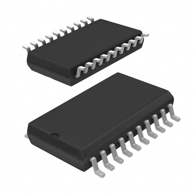
| 描述 | IC D-TYPE POS TRG SNGL 20SOP触发器 3-ST Oct D Flip-Flop |
| 产品分类 | |
| 品牌 | Fairchild Semiconductor |
| 产品手册 | |
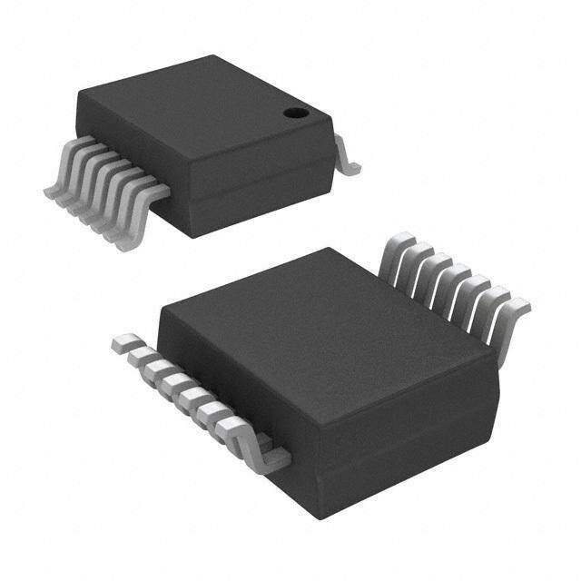
| 产品图片 |
|
| rohs | 符合RoHS无铅 / 符合限制有害物质指令(RoHS)规范要求 |
| 产品系列 | 逻辑集成电路,触发器,Fairchild Semiconductor MM74HC574SJX74HC |
| 数据手册 | |
| 产品型号 | MM74HC574SJX |
| 不同V、最大CL时的最大传播延迟 | 27ns @ 6V, 150pF |
| 产品种类 | 触发器 |
| 传播延迟时间 | 155 ns |
| 低电平输出电流 | 7.8 mA |
| 元件数 | 1 |
| 其它名称 | MM74HC574SJXCT |
| 功能 | 标准 |
| 包装 | 剪切带 (CT) |
| 单位重量 | 481.500 mg |
| 商标 | Fairchild Semiconductor |
| 安装类型 | 表面贴装 |
| 安装风格 | SMD/SMT |
| 封装 | Reel |
| 封装/外壳 | 20-SOIC(0.209",5.30mm 宽) |
| 封装/箱体 | SOP-20 |
| 工作温度 | -40°C ~ 85°C (TA) |
| 工厂包装数量 | 2000 |
| 最大工作温度 | + 85 C |
| 最小工作温度 | - 40 C |
| 极性 | Non-Inverting |
| 标准包装 | 1 |
| 每元件位数 | 8 |
| 电压-电源 | 2 V ~ 6 V |
| 电流-输出高,低 | 7.8mA,7.8mA |
| 电流-静态 | 8µA |
| 电源电压-最大 | 6 V |
| 电源电压-最小 | 2 V |
| 电路数量 | 8 |
| 类型 | D 型 |
| 系列 | MM74HC574 |
| 触发器类型 | 正边沿 |
| 输入电容 | 5pF |
| 输入类型 | Single-Ended |
| 输入线路数量 | 3 |
| 输出类型 | 三态, 非反相 |
| 输出线路数量 | 3 |
| 逻辑类型 | D-Type Edge Triggered Flip-Flop |
| 逻辑系列 | 74HC |
| 频率-时钟 | 35MHz |
| 高电平输出电流 | - 7.8 mA |


- 商务部:美国ITC正式对集成电路等产品启动337调查
- 曝三星4nm工艺存在良率问题 高通将骁龙8 Gen1或转产台积电
- 太阳诱电将投资9.5亿元在常州建新厂生产MLCC 预计2023年完工
- 英特尔发布欧洲新工厂建设计划 深化IDM 2.0 战略
- 台积电先进制程称霸业界 有大客户加持明年业绩稳了
- 达到5530亿美元!SIA预计今年全球半导体销售额将创下新高
- 英特尔拟将自动驾驶子公司Mobileye上市 估值或超500亿美元
- 三星加码芯片和SET,合并消费电子和移动部门,撤换高东真等 CEO
- 三星电子宣布重大人事变动 还合并消费电子和移动部门
- 海关总署:前11个月进口集成电路产品价值2.52万亿元 增长14.8%


PDF Datasheet 数据手册内容提取
Is Now Part of To learn more about ON Semiconductor, please visit our website at www.onsemi.com Please note: As part of the Fairchild Semiconductor integration, some of the Fairchild orderable part numbers will need to change in order to meet ON Semiconductor’s system requirements. Since the ON Semiconductor product management systems do not have the ability to manage part nomenclature that utilizes an underscore (_), the underscore (_) in the Fairchild part numbers will be changed to a dash (-). This document may contain device numbers with an underscore (_). Please check the ON Semiconductor website to verify the updated device numbers. The most current and up-to-date ordering information can be found at www.onsemi.com. Please email any questions regarding the system integration to Fairchild_questions@onsemi.com. ON Semiconductor and the ON Semiconductor logo are trademarks of Semiconductor Components Industries, LLC dba ON Semiconductor or its subsidiaries in the United States and/or other countries. ON Semiconductor owns the rights to a number of patents, trademarks, copyrights, trade secrets, and other intellectual property. A listing of ON Semiconductor’s product/patent coverage may be accessed at www.onsemi.com/site/pdf/Patent-Marking.pdf. ON Semiconductor reserves the right to make changes without further notice to any products herein. ON Semiconductor makes no warranty, representation or guarantee regarding the suitability of its products for any particular purpose, nor does ON Semiconductor assume any liability arising out of the application or use of any product or circuit, and specifically disclaims any and all liability, including without limitation special, consequential or incidental damages. Buyer is responsible for its products and applications using ON Semiconductor products, including compliance with all laws, regulations and safety requirements or standards, regardless of any support or applications information provided by ON Semiconductor. “Typical” parameters which may be provided in ON Semiconductor data sheets and/or specifications can and do vary in different applications and actual performance may vary over time. All operating parameters, including “Typicals” must be validated for each customer application by customer’s technical experts. ON Semiconductor does not convey any license under its patent rights nor the rights of others. ON Semiconductor products are not designed, intended, or authorized for use as a critical component in life support systems or any FDA Class 3 medical devices or medical devices with a same or similar classification in a foreign jurisdiction or any devices intended for implantation in the human body. Should Buyer purchase or use ON Semiconductor products for any such unintended or unauthorized application, Buyer shall indemnify and hold ON Semiconductor and its officers, employees, subsidiaries, affiliates, and distributors harmless against all claims, costs, damages, and expenses, and reasonable attorney fees arising out of, directly or indirectly, any claim of personal injury or death associated with such unintended or unauthorized use, even if such claim alleges that ON Semiconductor was negligent regarding the design or manufacture of the part. ON Semiconductor is an Equal Opportunity/Affirmative Action Employer. This literature is subject to all applicable copyright laws and is not for resale in any manner.
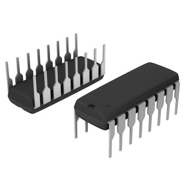
M September 1983 M Revised May 2005 7 4 H C 5 MM74HC574 7 4 3-STATE Octal D-Type Edge-Triggered Flip-Flop 3 - S T A General Description Features T E The MM74HC574 high speed octal D-type flip-flops utilize (cid:1) Typical propagation delay: 18 ns O advanced silicon-gate P-well CMOS technology. They pos- (cid:1) Wide operating voltage range: 2V–6V c soef sssta tnhdea hrdig Ch MnOoiSse i nimtemgruanteitdy cainrcdu liotsw, apso wweelrl caosn tshuem apbtiiloitny (cid:1) Low input current: 1 PA maximum ta to drive 15LS-TTL loads. Due to the large output drive (cid:1) Low quiescent current: 80 PA maximum l D capability and the 3-STATE feature, these devices are ide- (cid:1) Compatible with bus-oriented systems - T ally suited for interfacing with bus lines in a bus organized (cid:1) Output drive capability: 15 LS-TTL loads y system. p e These devices are positive edge triggered flip-flops. Data E at the D inputs, meeting the set-up and hold time require- d ments, are transferred to the Q outputs on positive going g transitions of the CLOCK (CK) input. When a high logic e level is applied to the OUTPUT CONTROL (OC) input, all -T outputs go to a high impedance state, regardless of what r i signals are present at the other inputs and the state of the g g storage elements. e The 74HC logic family is speed, function, and pinout com- re patible with the standard 74LS logic family. All inputs are d protected from damage due to static discharge by internal F diode clamps to VCC and ground. lip - F lo Ordering Code: p Order Number Package Number Package Description MM74HC574WM M20B 20-Lead Small Outline Integrated Circuit (SOIC), JEDEC MS-013, 0.300" Wide MM74HC574SJ M20D 20-Lead Small Outline Package (SOP), EIAJ TYPE II, 5.3mm Wide MM74HC574MTC MTC20 20-Lead Thin Shrink Small Outline Package (TSSOP), JEDEC MO-153, 4.4mm Wide MM74HC574N N20A 20-Lead Plastic Dual-In-Line Package (PDIP), JEDEC MS-001, 0.300" Wide Devices also available in Tape and Reel. Specify by appending the suffix letter “X” to the ordering code. Connection Diagram Truth Table Pin Assignments for DIP, SOIC, SOP and TSSOP Output Clock Data Output Control L n H H L n L L L L X Q0 H X X Z H HIGH Level L LOW Level X Don't Care n Transition from LOW-to-HIGH Z High Impedance State Q0 The level of the output before steady state input conditions were established Top View © 2005 Fairchild Semiconductor Corporation DS005213 www.fairchildsemi.com
4 7 Absolute Maximum Ratings Recommended Operating 5 (Note 1) C (Note 2) Conditions H 74 Supply Voltage (VCC) (cid:16)0.5 to (cid:14)7.0V Min Max Units M DC Input Voltage (VIN) (cid:16)1.5 to VCC (cid:14)1.5V Supply Voltage (VCC) 2 6 V M DC Output Voltage (VOUT) (cid:16)0.5 to VCC (cid:14)0.5V DC Input or Output Voltage 0 VCC V Clamp Diode Current (IIK, IOK) r20 mA (VIN,VOUT) DC Output Current, per pin (IOUT) r35 mA Operating Temperature Range (TA) (cid:16)40 (cid:14)85 qC DC VCC or GND Current, per pin (ICC) r70 mA Input Rise or Fall Times Storage Temperature Range (TSTG) (cid:16)65qC to (cid:14)150qC (tr, tf) VCC 2.0V 1000 ns Power Dissipation (PD) VCC 4.5V 500 ns (Note 3) 600 mW VCC 6.0V 400 ns S.O. Package only 500 mW Note 1: Maximum Ratings are those values beyond which damage to the Lead Temperature (TL) device may occur. Note 2: Unless otherwise specified all voltages are referenced to ground. (Soldering 10 seconds) 260qC Note 3: Power Dissipation temperature derating — plastic “N” package: (cid:16) 12 mW/qC from 65qC to 85qC. DC Electrical Characteristics (Note 4) Symbol Parameter Conditions VCC TA 25qC TA (cid:16)40 to 85qC TA (cid:16)55 to 125qC Units Typ Guaranteed Limits VIH Minimum HIGH Level Input 2.0V 1.5 1.5 1.5 Voltage 4.5V 3.15 3.15 3.15 V 6.0V 4.2 4.2 4.2 VIL Maximum LOW Level Input 2.0V 0.5 0.5 0.5 Voltage 4.5V 1.35 1.35 1.35 V 6.0V 1.8 1.8 1.8 VOH Minimum HIGH Level Output VIN VIH or VIL Voltage |IOUT| d 20 PA 2.0V 2.0 1.9 1.9 1.9 4.5V 4.5 4.4 4.4 4.4 V 6.0V 6.0 5.9 5.9 5.9 VIN VIH or VIL |IOUT| d 6.0 mA 4.5V 4.2 3.98 3.84 3.7 V |IOUT| d 7.8 mA 6.0V 5.7 5.48 5.34 5.2 VOL Maximum LOW Level Output VIN VIH or VIL Voltage |IOUT| d 20 PA 2.0V 0 0.1 0.1 0.1 4.5V 0 0.1 0.1 0.1 V 6.0V 0 0.1 0.1 0.1 VIN VIH or VIL |IOUT| d 6.0 mA 4.5V 0.2 0.26 0.33 0.4 V |IOUT| d 7.8 mA 6.0V 0.2 0.26 0.33 0.4 IIN Maximum Input Current VIN VCC or GND 6.0V r0.1 r1.0 r1.0 PA IOZ Maximum 3-STATE VOUT VCC or GND Output Leakage Current OC VIH 6.0V r0.5 r5.0 r10 PA ICC Maximum Quiescent Supply VIN VCC or GND Current IOUT 0 PA 6.0V 8.0 80 160 PA ’ICC Quiescent Supply Current VCC 5.5V OE 1.0 1.5 1.8 2.0 per Input Pin VIN 2.4V CLK 0.6 0.8 1.0 1.1 mA or 0.4V (Note 4) DATA 0.4 0.5 0.6 0.7 Note 4: For a power supply of 5V r10% the worst-case output voltages (VOH, and VOL) occur for HC at 4.5V. Thus the 4.5V values should be used when designing with this supply. Worst-case VIH and VIL occur at VCC 5.5V and 4.5V respectively. (The VIH value at 5.5V is 3.85V.) The worst-case leakage cur- rent (IIN, ICC, and IOZ) occur for CMOS at the higher voltage and so the 6.0V values should be used. www.fairchildsemi.com 2
M AC Electrical Characteristics M 7 VCC 5V, TA 25qC, tr tf 6 ns 4 Guaranteed H Symbol Parameter Conditions Typ Units C Limit 5 fMAX Maximum Operating Frequency 60 33 MHz 7 4 tPHL, tPLH Maximum Propagation Delay, Clock to Q CL 45 pF 17 27 ns tPZH, tPZL Maximum Output Enable Time RL 1 k: 19 28 ns CL 45 pF tPHZ, tPLZ Maximum Output Disable Time RL 1 k: 14 25 ns CL 5 pF tS Minimum Setup Time, Data to Clock 10 12 ns tH Minimum Hold Time, Clock to Data (cid:16)3 5 ns tW Minimum Pulse Clock Width 8 15 ns AC Electrical Characteristics VCC 2.0 (cid:16) 6.0V, CL 50 pF, tr tf 6 ns (unless otherwise specified) Symbol Parameter Conditions VCC TA 25qC TA (cid:16)40 to 85qC TA (cid:16)55 to 125qC Units Typ Guaranteed Limits fMAX Maximum Operating Frequency CL 50 pF 2.0V 33 28 23 4.5V 30 24 20 MHz 6.0V 35 28 23 tPHL, tPLH Maximum Propagation CL 50 pF 2.0V 18 30 38 45 ns Delay, Clock to Q CL 150 pF 2.0V 51 155 194 233 CL 50 pF 4.5V 13 23 29 35 ns CL 150 pF 4.5V 19 31 47 47 CL 50 pF 6.0V 12 20 25 30 ns CL 150 pF 6.0V 18 27 34 41 tPZH, tPZL Maximum Output Enable RL 1 k: Time CL 50 pF 2.0V 22 30 38 45 ns CL 150 pF 2.0V 59 180 225 270 CL 50 pF 4.5V 14 28 35 42 ns CL 150 pF 4.5V 20 36 45 54 CL 50 pF 6.0V 12 24 30 36 ns CL 150 pF 6.0V 18 31 39 47 tPHZ, tPLZ Maximum Output Disable Time RL 1 k: 2.0V 15 30 38 45 CL 50 pF 4.5V 12 25 31 38 ns 6.0V 10 21 27 32 tS Minimum Setup Time 2.0V 6 12 15 18 Data to Clock 4.5V 20 25 30 ns 6.0V 17 21 25 tH Minimum Hold Time 2.0V (cid:16)1 5 6 8 Clock to Data 4.5V 0 0 0 ns 6.0V 0 0 0 tTHL, tTLH Maximum Output Rise CL 50 pF 2.0V 6 12 15 18 and Fall Time 4.5V 7 12 15 18 ns 6.0V 6 10 13 15 tW Minimum Clock Pulse Width 2.0V 30 15 20 24 4.5V 9 16 20 24 ns 6.0V 8 14 18 20 tr,tf Maximum Clock Input Rise 2.0V 1000 1000 1000 and Fall Time 4.5V 500 500 500 ns 6.0V 400 400 400 CPD Power Dissipation Capacitance OC VCC 5 pF (Note 5) (per latch) OC GND 58 CIN Maximum Input Capacitance 5 10 10 10 pF 3 www.fairchildsemi.com
4 7 AC Electrical Characteristics 5 (Continued) C H 74 Symbol Parameter Conditions VCC TA 25qC TA (cid:16)40 to 85qC TA (cid:16)55 to 125qC Units M Typ Guaranteed Limits M COUT Maximum Output 15 20 20 20 pF Capacitance Note 5: CPD determines the no load dynamic power consumption, PD CPD VCC2 f (cid:14) ICC VCC, and the no load dynamic current consumption, IS CPD VCC f (cid:14) ICC. www.fairchildsemi.com 4
M Physical Dimensions inches (millimeters) unless otherwise noted M 7 4 H C 5 7 4 20-Lead Small Outline Integrated Circuit (SOIC), JEDEC MS-013, 0.300" Wide Package Number M20B 5 www.fairchildsemi.com
4 7 Physical Dimensions 5 inches (millimeters) unless otherwise noted (Continued) C H 4 7 M M 20-Lead Small Outline Package (SOP), EIAJ TYPE II, 5.3mm Wide Package Number M20D www.fairchildsemi.com 6
M Physical Dimensions inches (millimeters) unless otherwise noted (Continued) M 7 4 H C 5 7 4 20-Lead Thin Shrink Small Outline Package (TSSOP), JEDEC MO-153, 4.4mm Wide Package Number MTC20 7 www.fairchildsemi.com
p o Physical Dimensions inches (millimeters) unless otherwise noted (Continued) l F - p li F d e r e g g i r T - e g d E e p y T - D l a t c O E T A 20-Lead Plastic Dual-In-Line Package (PDIP), JEDEC MS-001, 0.300" Wide T S Package Number N20A - 3 4 7 5 C H 4 7 M M Fairchild does not assume any responsibility for use of any circuitry described, no circuit patent licenses are implied and Fairchild reserves the right at any time without notice to change said circuitry and specifications. LIFE SUPPORT POLICY FAIRCHILD’S PRODUCTS ARE NOT AUTHORIZED FOR USE AS CRITICAL COMPONENTS IN LIFE SUPPORT DEVICES OR SYSTEMS WITHOUT THE EXPRESS WRITTEN APPROVAL OF THE PRESIDENT OF FAIRCHILD SEMICONDUCTOR CORPORATION. As used herein: 1. Life support devices or systems are devices or systems 2. A critical component in any component of a life support which, (a) are intended for surgical implant into the device or system whose failure to perform can be rea- body, or (b) support or sustain life, and (c) whose failure sonably expected to cause the failure of the life support to perform when properly used in accordance with device or system, or to affect its safety or effectiveness. instructions for use provided in the labeling, can be rea- sonably expected to result in a significant injury to the www.fairchildsemi.com user. www.fairchildsemi.com 8
ON Semiconductor and are trademarks of Semiconductor Components Industries, LLC dba ON Semiconductor or its subsidiaries in the United States and/or other countries. ON Semiconductor owns the rights to a number of patents, trademarks, copyrights, trade secrets, and other intellectual property. A listing of ON Semiconductor’s product/patent coverage may be accessed at www.onsemi.com/site/pdf/Patent−Marking.pdf. ON Semiconductor reserves the right to make changes without further notice to any products herein. ON Semiconductor makes no warranty, representation or guarantee regarding the suitability of its products for any particular purpose, nor does ON Semiconductor assume any liability arising out of the application or use of any product or circuit, and specifically disclaims any and all liability, including without limitation special, consequential or incidental damages. Buyer is responsible for its products and applications using ON Semiconductor products, including compliance with all laws, regulations and safety requirements or standards, regardless of any support or applications information provided by ON Semiconductor. “Typical” parameters which may be provided in ON Semiconductor data sheets and/or specifications can and do vary in different applications and actual performance may vary over time. All operating parameters, including “Typicals” must be validated for each customer application by customer’s technical experts. ON Semiconductor does not convey any license under its patent rights nor the rights of others. ON Semiconductor products are not designed, intended, or authorized for use as a critical component in life support systems or any FDA Class 3 medical devices or medical devices with a same or similar classification in a foreign jurisdiction or any devices intended for implantation in the human body. Should Buyer purchase or use ON Semiconductor products for any such unintended or unauthorized application, Buyer shall indemnify and hold ON Semiconductor and its officers, employees, subsidiaries, affiliates, and distributors harmless against all claims, costs, damages, and expenses, and reasonable attorney fees arising out of, directly or indirectly, any claim of personal injury or death associated with such unintended or unauthorized use, even if such claim alleges that ON Semiconductor was negligent regarding the design or manufacture of the part. ON Semiconductor is an Equal Opportunity/Affirmative Action Employer. This literature is subject to all applicable copyright laws and is not for resale in any manner. PUBLICATION ORDERING INFORMATION LITERATURE FULFILLMENT: N. American Technical Support: 800−282−9855 Toll Free ON Semiconductor Website: www.onsemi.com Literature Distribution Center for ON Semiconductor USA/Canada 19521 E. 32nd Pkwy, Aurora, Colorado 80011 USA Europe, Middle East and Africa Technical Support: Order Literature: http://www.onsemi.com/orderlit Phone: 303−675−2175 or 800−344−3860 Toll Free USA/Canada Phone: 421 33 790 2910 Fax: 303−675−2176 or 800−344−3867 Toll Free USA/Canada Japan Customer Focus Center For additional information, please contact your local Email: orderlit@onsemi.com Phone: 81−3−5817−1050 Sales Representative © Semiconductor Components Industries, LLC www.onsemi.com www.onsemi.com 1
Mouser Electronics Authorized Distributor Click to View Pricing, Inventory, Delivery & Lifecycle Information: O N Semiconductor: MM74HC574MTCX MM74HC574WMX MM74HC574SJX MM74HC574N MM74HC574MTC MM74HC574SJ MM74HC574WM