 Datasheet下载
- 型号: SN74AUP1G74DCUR
- 制造商: Texas Instruments
- 库位|库存: xxxx|xxxx
- 要求:
| 数量阶梯 | 香港交货 | 国内含税 |
| +xxxx | $xxxx | ¥xxxx |
查看当月历史价格
查看今年历史价格
SN74AUP1G74DCUR产品简介:
ICGOO电子元器件商城为您提供SN74AUP1G74DCUR由Texas Instruments设计生产,在icgoo商城现货销售,并且可以通过原厂、代理商等渠道进行代购。 SN74AUP1G74DCUR价格参考¥1.05-¥1.05。Texas InstrumentsSN74AUP1G74DCUR封装/规格:逻辑 - 触发器, Flip Flop 1 Element D-Type 1 Bit Positive Edge 8-VFSOP (0.091", 2.30mm Width)。您可以下载SN74AUP1G74DCUR参考资料、Datasheet数据手册功能说明书,资料中有SN74AUP1G74DCUR 详细功能的应用电路图电压和使用方法及教程。
SN74AUP1G74DCUR是Texas Instruments(德州仪器)生产的一款单路正沿触发D型触发器,属于超低功耗、高性能的AUP系列逻辑器件。该芯片采用6引脚SC-70封装,适用于对空间和功耗要求严格的便携式电子设备。

其主要应用场景包括:

1. 移动通信设备:广泛应用于智能手机、平板电脑等便携设备中,用于信号同步、电平转换和数据锁存,因其低静态电流显著延长电池寿命。

2. 消费类电子产品:在可穿戴设备(如智能手表、健康监测仪)中,用于时序控制和状态保持,满足小型化与低功耗需求。

3. 工业传感器与物联网节点:在低功耗传感系统中实现数据采样和边沿触发控制,支持长时间待机下的稳定运行。

4. 电源管理与时序控制电路:作为时钟分频器或脉冲整形电路,用于精确控制信号时序,提升系统稳定性。

5. 接口缓冲与电平转换:在不同电压域之间传输数字信号,实现1.8V至3.3V系统的兼容通信。

SN74AUP1G74DCUR具备宽电压工作范围(1.7V至3.6V)、高噪声抑制能力和良好的驱动性能,适合高频、低延迟的数字逻辑设计。其单触发器结构灵活,便于集成于紧凑型PCB布局中,是现代低功耗嵌入式系统中的理想选择。
| 参数 | 数值 |
| 产品目录 | 集成电路 (IC)半导体 |
| 描述 | IC D-TYPE POS TRG SNGL US8触发器 LoPwSnglPosEdgTrggrd DTypeFlipFlop |
| 产品分类 | |
| 品牌 | Texas Instruments |
| 产品手册 | |
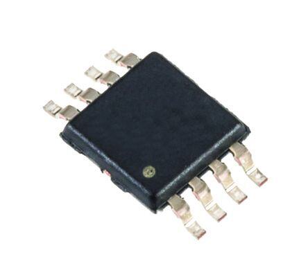
| 产品图片 |
|
| rohs | 符合RoHS无铅 / 符合限制有害物质指令(RoHS)规范要求 |
| 产品系列 | 逻辑集成电路,触发器,Texas Instruments SN74AUP1G74DCUR74AUP |
| 数据手册 | |
| 产品型号 | SN74AUP1G74DCUR |
| 不同V、最大CL时的最大传播延迟 | 7ns @ 3.3V, 30pF |
| 产品目录页面 | |
| 产品种类 | 触发器 |
| 传播延迟时间 | 27 ns |
| 低电平输出电流 | 4 mA |
| 元件数 | 1 |
| 其它名称 | 296-19761-6 |
| 功能 | 设置(预设)和复位 |
| 包装 | Digi-Reel® |
| 商标 | Texas Instruments |
| 安装类型 | 表面贴装 |
| 安装风格 | SMD/SMT |
| 封装 | Reel |
| 封装/外壳 | 8-VFSOP(0.091",2.30mm 宽) |
| 封装/箱体 | VSSOP-8 |
| 工作温度 | -40°C ~ 85°C |
| 工厂包装数量 | 3000 |
| 最大工作温度 | + 85 C |
| 最小工作温度 | - 40 C |
| 极性 | Inverting/Non-Inverting |
| 标准包装 | 1 |
| 每元件位数 | 1 |
| 电压-电源 | 0.8 V ~ 3.6 V |
| 电流-输出高,低 | 4mA,4mA |
| 电流-静态 | 0.5µA |
| 电源电压-最大 | 3.6 V |
| 电源电压-最小 | 0.8 V |
| 电路数量 | 1 |
| 类型 | D 型 |
| 系列 | SN74AUP1G74 |
| 触发器类型 | 正边沿 |
| 输入电容 | 1.5pF |
| 输入类型 | Single-Ended |
| 输入线路数量 | 1 |
| 输出类型 | 差分 |
| 输出线路数量 | 1 |
| 逻辑类型 | Single-Gate |
| 逻辑系列 | AUP |
| 频率-时钟 | 100MHz |
| 高电平输出电流 | - 4 mA |


- 商务部:美国ITC正式对集成电路等产品启动337调查
- 曝三星4nm工艺存在良率问题 高通将骁龙8 Gen1或转产台积电
- 太阳诱电将投资9.5亿元在常州建新厂生产MLCC 预计2023年完工
- 英特尔发布欧洲新工厂建设计划 深化IDM 2.0 战略
- 台积电先进制程称霸业界 有大客户加持明年业绩稳了
- 达到5530亿美元!SIA预计今年全球半导体销售额将创下新高
- 英特尔拟将自动驾驶子公司Mobileye上市 估值或超500亿美元
- 三星加码芯片和SET,合并消费电子和移动部门,撤换高东真等 CEO
- 三星电子宣布重大人事变动 还合并消费电子和移动部门
- 海关总署:前11个月进口集成电路产品价值2.52万亿元 增长14.8%


PDF Datasheet 数据手册内容提取
Product Sample & Technical Tools & Support & Folder Buy Documents Software Community SN74AUP1G74 SCES644D–MARCH2006–REVISEDDECEMBER2015 SN74AUP1G74 Low-Power Single Positive-Edge-Triggered D-Type Flip-Flop With Clear and Preset 1 Features 2 Applications • AvailableintheTexasInstruments NanoStar™ • Servers 1 Package • LEDDisplays • LowStatic-PowerConsumption: • NetworkSwitches I =0.9μAMaximum CC • TelecomInfrastructure • LowDynamic-PowerConsumption: • MotorDrivers C =5.5pFTypicalat3.3V pd • I/OExpanders • LowInputCapacitance:C =1.5pFTypical i • LowNoise–OvershootandUndershoot 3 Description <10%ofV CC The AUP family is TI's premier solution to the • I SupportsPartial-Power-DownModeOperation industry's low-power needs in battery-powered off portable applications. This family ensures a very low • Schmitt-TriggerActionAllowsSlowInput static- and dynamic-power consumption across the TransitionandBetterSwitchingNoiseImmunityat entire V range of 0.8 V to 3.6 V, resulting in theInput CC increased battery life. This product also maintains (V =250mVTypicalat3.3V) hys excellent signal integrity (see the very low undershoot • WideOperatingVCCRangeof0.8Vto3.6V andovershootcharacteristicsshowninFigure6). • Optimizedfor3.3-VOperation DeviceInformation(1) • 3.6-VI/OToleranttoSupportMixed-ModeSignal Operation PARTNUMBER PACKAGE BODYSIZE(NOM) SN74AUP1G74YFP DSBGA(8) 1.56mm×0.76mm • t =5nsMaximumat3.3V pd SN74AUP1G74YZP DSBGA(8) 1.86mm×0.89mm • SuitableforPoint-to-PointApplications SN74AUP1G74DCU VSSOP(8) 2.30mm×2.00mm • Latch-UpPerformanceExceeds100mAPer SN74AUP1G74DQE X2SON(8) 1.40mm×1.00mm JESD78,ClassII SN74AUP1G74RSE UQFN(8) 1.50mm×1.50mm • ESDPerformanceTestedPerJESD22 (1) For all available packages, see the orderable addendum at – 2000-VHuman-BodyModel(A114-B,ClassII) theendofthedatasheet. – 1000-VCharged-DeviceModel(C101) AUP–TheLowest-PowerFamily 6 CLR CLK 1 C C C 3 Q TG 5 C C C Q C 2 D TG TG TG C C C 7 PRE 1 An IMPORTANT NOTICE at the end of this data sheet addresses availability, warranty, changes, use in safety-critical applications, intellectualpropertymattersandotherimportantdisclaimers.PRODUCTIONDATA.
SN74AUP1G74 SCES644D–MARCH2006–REVISEDDECEMBER2015 www.ti.com Table of Contents 1 Features.................................................................. 1 7.2 EnableandDisableTimes......................................14 2 Applications........................................................... 1 8 DetailedDescription............................................ 15 3 Description............................................................. 1 8.1 Overview.................................................................15 4 RevisionHistory..................................................... 2 8.2 FunctionalBlockDiagram.......................................15 8.3 FeatureDescription.................................................15 5 PinConfigurationandFunctions......................... 3 8.4 DeviceFunctionalModes........................................15 6 Specifications......................................................... 4 9 ApplicationandImplementation........................ 16 6.1 AbsoluteMaximumRatings .....................................4 9.1 ApplicationInformation ..........................................16 6.2 ESDRatings ............................................................4 9.2 TypicalPowerButtonCircuit..................................16 6.3 RecommendedOperatingConditions......................4 10 PowerSupplyRecommendations..................... 17 6.4 ThermalInformation..................................................5 6.5 ElectricalCharacteristics,T =25°C........................5 11 Layout................................................................... 17 A 6.6 ElectricalCharacteristics,T =–40°Cto+85°C.......6 11.1 LayoutGuidelines.................................................17 A 6.7 TimingRequirements................................................7 11.2 LayoutExample....................................................17 6.8 SwitchingCharacteristics,C =5pF........................8 12 DeviceandDocumentationSupport................. 18 L 6.9 SwitchingCharacteristics,C =10pF......................9 12.1 DocumentationSupport........................................18 L 6.10 SwitchingCharacteristics,C =15pF..................10 12.2 CommunityResources..........................................18 L 6.11 SwitchingCharacteristics,C =30pF..................11 12.3 Trademarks...........................................................18 L 6.12 OperatingCharacteristics......................................12 12.4 ElectrostaticDischargeCaution............................18 6.13 TypicalCharacteristics..........................................12 12.5 Glossary................................................................18 7 ParameterMeasurementInformation ...............13 13 Mechanical,Packaging,andOrderable 7.1 PropagationDelays,SetupandHoldTimes,and Information........................................................... 18 PulseWidth).............................................................13 4 Revision History NOTE:Pagenumbersforpreviousrevisionsmaydifferfrompagenumbersinthecurrentversion. ChangesfromRevisionC(March2010)toRevisionD Page • AddedPinConfigurationandFunctionssection,ESDRatingstable,FeatureDescriptionsection,DeviceFunctional Modes,ApplicationandImplementationsection,PowerSupplyRecommendationssection,Layoutsection,Device andDocumentationSupportsection,andMechanical,Packaging,andOrderableInformationsection .............................. 1 2 SubmitDocumentationFeedback Copyright©2006–2015,TexasInstrumentsIncorporated ProductFolderLinks:SN74AUP1G74
SN74AUP1G74 www.ti.com SCES644D–MARCH2006–REVISEDDECEMBER2015 5 Pin Configuration and Functions DCUPackage 8-PinVSSOP DQEPackage TopView 8-PinX2SON TopView CLK 1 8 VCC CLK 1 8 VCC D 2 7 PRE D 2 7 PRE Q 3 6 CLR Q 3 6 CLR GND 4 5 Q GND 4 5 Q YFPorYZPPackage RSEPackage 8-PinDSBGA 8-PinUQFN TopView TopView V CLK A1 18 A2 V CC CC D B1 27 B2 PRE PRE 1 8 7 CLK Q C1 36 C2 CLR GND D1 45 D2 Q CLR 2 6 D Q 3 4 5 Q GND PinFunctions(1) PIN VSSOP, I/O DESCRIPTION NAME UQFN DSBGA X2SON CLK 1 7 A1 I Risingedgetriggeredclocksignalinput CLR 6 2 C2 I Clear,Activelow D 2 6 B1 I Datainput GND 4 4 D1 — Ground PRE 7 1 B2 I Preset,Activelow Q 5 3 D2 O Output Q 3 5 C1 O Invertedoutput V 8 8 A2 — Powersupply CC (1) SeeMechanical,Packaging,andOrderableInformationfordimensions. Copyright©2006–2015,TexasInstrumentsIncorporated SubmitDocumentationFeedback 3 ProductFolderLinks:SN74AUP1G74
SN74AUP1G74 SCES644D–MARCH2006–REVISEDDECEMBER2015 www.ti.com 6 Specifications 6.1 Absolute Maximum Ratings overoperatingfree-airtemperaturerange(unlessotherwisenoted)(1) MIN MAX UNIT V Supplyvoltage –0.5 4.6 V CC V Inputvoltage(2) –0.5 4.6 V I V Voltageappliedtoanyoutputinthehigh-impedanceorpower-offstate(2) –0.5 4.6 V O V Outputvoltageinthehighorlowstate(2) –0.5 V +0.5 V O CC I Inputclampcurrent V <0 –50 mA IK I I Outputclampcurrent V <0 –50 mA OK O I Continuousoutputcurrent ±20 mA O ContinuouscurrentthroughV orGND ±50 mA CC T Junctiontemperature 150 J °C T Storagetemperature –65 150 stg (1) StressesbeyondthoselistedunderAbsoluteMaximumRatingsmaycausepermanentdamagetothedevice.Thesearestressratings only,whichdonotimplyfunctionaloperationofthedeviceattheseoranyotherconditionsbeyondthoseindicatedunderRecommended OperatingConditions.Exposuretoabsolute-maximum-ratedconditionsforextendedperiodsmayaffectdevicereliability. (2) Theinputnegative-voltageandoutputvoltageratingsmaybeexceedediftheinputandoutputcurrentratingsareobserved. 6.2 ESD Ratings VALUE UNIT Electrostatic Human-bodymodel(HBM),perANSI/ESDA/JEDECJS-001(1) ±2000 V V (ESD) discharge Charged-devicemodel(CDM),perJEDECspecificationJESD22-C101(2) ±1000 (1) JEDECdocumentJEP155statesthat500-VHBMallowssafemanufacturingwithastandardESDcontrolprocess. (2) JEDECdocumentJEP157statesthat250-VCDMallowssafemanufacturingwithastandardESDcontrolprocess. 6.3 Recommended Operating Conditions(1) MIN MAX UNIT V Supplyvoltage 0.8 3.6 V CC V =0.8V V CC CC V =1.1Vto1.95V 0.7×V CC CC V High-levelinputvoltage V IH V =2.3Vto2.7V 1.6 CC V =3Vto3.6V 2 CC V =0.8V 0 CC V =1.1Vto1.95V 0.3×V CC CC V Low-levelinputvoltage V IL V =2.3Vto2.7V 0.7 CC V =3Vto3.6V 0.9 CC V Inputvoltage 0 3.6 V I V Outputvoltage 0 V V O CC V =0.8V –20 μA CC V =1.1V –1.1 CC V =1.4V –1.7 CC I High-leveloutputcurrent OH V =1.65 –1.9 mA CC V =2.3V –3.1 CC V =3V –4 CC (1) AllunusedinputsofthedevicemustbeheldatV orGNDtoensureproperdeviceoperation.SeetheTIapplicationreport, CC ImplicationsofSloworFloatingCMOSInputs,SCBA004. 4 SubmitDocumentationFeedback Copyright©2006–2015,TexasInstrumentsIncorporated ProductFolderLinks:SN74AUP1G74
SN74AUP1G74 www.ti.com SCES644D–MARCH2006–REVISEDDECEMBER2015 Recommended Operating Conditions(1) (continued) MIN MAX UNIT V =0.8V 20 μA CC V =1.1V 1.1 CC V =1.4V 1.7 CC I Low-leveloutputcurrent OL V =1.65V 1.9 mA CC V =2.3V 3.1 CC V =3V 4 CC Δt/Δv Inputtransitionriseorfallrate V =0.8Vto3.6V 200 ns/V CC T Operatingfree-airtemperature –40 85 °C A 6.4 Thermal Information SN74AUP1G74 DCU DQE RSE YFP/YZP THERMALMETRIC(1) UNIT (VSSOP) (X2SON) (UQFN) (DSBGA) 8PINS 8PINS 8PINS 8PINS R Junction-to-ambientthermalresistance 227 261 253 102 °C/W θJA (1) Formoreinformationabouttraditionalandnewthermalmetrics,seetheSemiconductorandICPackageThermalMetricsapplication report,SPRA953. 6.5 Electrical Characteristics, T = 25°C A overrecommendedoperatingfree-airtemperaturerange(unlessotherwisenoted) PARAMETER TESTCONDITIONS V MIN TYP MAX UNIT CC I =–20μA 0.8Vto3.6V V –0.1 OH CC I =–1.1mA 1.1V 0.7×V OH CC I =–1.7mA 1.4V 1.11 OH I =–1.9mA 1.65V 1.32 OH V V OH I =–2.3mA 2.05 OH 2.3V I =–3.1mA 1.9 OH I =–2.7mA 2.72 OH 3V I =–4mA 2.6 OH I =20μA 0.8Vto3.6V 0.1 OL I =1.1mA 1.1V 0.3×V OL CC I =1.7mA 1.4V 0.31 OL I =1.9mA 1.65V 0.31 OL V V OL I =2.3mA 0.31 OL 2.3V I =3.1mA 0.44 OL I =2.7mA 0.31 OL 3V I =4mA 0.44 OL I AorBinput V =GNDto3.6V 0Vto3.6V 0.1 μA I I I V orV =0Vto3.6V 0V 0.2 μA off I O ΔI V orV =0Vto3.6V 0Vto0.2V 0.2 μA off I O V =GNDor(V to3.6V), I I CC 0.8Vto3.6V 0.5 μA CC I =0 O ΔI V =V –0.6V(1),I =0 3.3V 40 μA CC I CC O 0V 1.5 C V =V orGND pF i I CC 3.6V 1.5 C V =GND 0V 3 pF o O (1) OneinputatV –0.6V,otherinputatV orGND CC CC Copyright©2006–2015,TexasInstrumentsIncorporated SubmitDocumentationFeedback 5 ProductFolderLinks:SN74AUP1G74
SN74AUP1G74 SCES644D–MARCH2006–REVISEDDECEMBER2015 www.ti.com 6.6 Electrical Characteristics, T = –40°C to +85°C A overrecommendedoperatingfree-airtemperaturerange(unlessotherwisenoted) PARAMETER TESTCONDITIONS V MIN TYP MAX UNIT CC I =–20μA 0.8Vto3.6V V –0.1 OH CC I =–1.1mA 1.1V 0.7×V OH CC I =–1.7mA 1.4V 1.03 OH I =–1.9mA 1.65V 1.3 OH V V OH I =–2.3mA 1.97 OH 2.3V I =–3.1mA 1.85 OH I =–2.7mA 2.67 OH 3V I =–4mA 2.55 OH I =20μA 0.8Vto3.6V 0.1 OL I =1.1mA 1.1V 0.3×V OL CC I =1.7mA 1.4V 0.37 OL I =1.9mA 1.65V 0.35 OL V V OL I =2.3mA 0.33 OL 2.3V I =3.1mA 0.45 OL I =2.7mA 0.33 OL 3V I =4mA 0.45 OL I AorBinput V =GNDto3.6V 0Vto3.6V 0.5 μA I I I V orV =0Vto3.6V 0V 0.6 μA off I O ΔI V orV =0Vto3.6V 0Vto0.2V 0.6 μA off I O V =GNDor(V to3.6V), I I CC 0.8Vto3.6V 0.9 μA CC I =0 O ΔI V =V –0.6V(1),I =0 3.3V 50 μA CC I CC O 0V C V =V orGND pF i I CC 3.6V C V =GND 0V pF o O (1) OneinputatV –0.6V,otherinputatV orGND CC CC 6 SubmitDocumentationFeedback Copyright©2006–2015,TexasInstrumentsIncorporated ProductFolderLinks:SN74AUP1G74
SN74AUP1G74 www.ti.com SCES644D–MARCH2006–REVISEDDECEMBER2015 6.7 Timing Requirements overrecommendedoperatingfree-airtemperaturerange(unlessotherwisenoted)(seeFigure3) V MIN(1) TYP(2) MAX(1) UNIT CC 0.8V 21 1.2V±0.1V 40 1.5V±0.1V 50 f Clockfrequency MHz clock 1.8V±0.15V 60 2.5V±0.2V 90 3.3V±0.3V 90 0.8V 3.5 1.2V±0.1V 2 1.5V±0.1V 2 CLKhighorlow 1.8V±0.15V 2 2.5V±0.2V 2 3.3V±0.3V 2 t Pulseduration ns w 0.8V 4.5 1.2V±0.1V 2 1.5V±0.1V 2 PREorCLRlow 1.8V±0.15V 2 2.5V±0.2V 2 3.3V±0.3V 2 0.8V 3 1.2V±0.1V 1.3 1.5V±0.1V 1 Datahigh 1.8V±0.15V 1 2.5V±0.2V 0.5 3.3V±0.3V 0.5 0.8V 1 1.2V±0.1V 1.2 1.5V±0.1V 1 t SetuptimebeforeCLK↑ Datalow ns su 1.8V±0.15V 1 2.5V±0.2V 1 3.3V±0.3V 1 0.8V 1 1.2V±0.1V 0.5 1.5V±0.1V 0.5 PREorCLRinactive 1.8V±0.15V 0.5 2.5V±0.2V 0.5 3.3V±0.3V 0.5 0.8V 0 1.2V±0.1V 0 1.5V±0.1V 0 t Holdtime,dataafterCLK↑ ns h 1.8V±0.15V 0 2.5V±0.2V 0 3.3V±0.3V 0 (1) MinimumandmaximumvaluesareforT =–40°Cto+85°C A (2) TypicalsareforT =25°C A Copyright©2006–2015,TexasInstrumentsIncorporated SubmitDocumentationFeedback 7 ProductFolderLinks:SN74AUP1G74
SN74AUP1G74 SCES644D–MARCH2006–REVISEDDECEMBER2015 www.ti.com 6.8 Switching Characteristics, C = 5 pF L overrecommendedoperatingfree-airtemperaturerange,C =5pF(unlessotherwisenoted)(seeFigure3andFigure4) L FROM TO PARAMETER (INPUT) (OUTPUT) VCC TA MIN TYP MAX UNIT 0.8V TA=25°C 60 TA=25°C 80 1.2V±0.1V TA=–40°Cto85°C 60 TA=25°C 125 1.5V±0.1V TA=–40°Cto85°C 90 fmax TA=25°C 150 MHz 1.8V±0.15V TA=–40°Cto85°C 120 TA=25°C 180 2.5V±0.2V TA=–40°Cto85°C 160 TA=25°C 190 3.3V±0.3V TA=–40°Cto85°C 180 0.8V TA=25°C 31 TA=25°C 2 10 20 1.2V±0.1V TA=–40°Cto85°C 2.7 20.4 TA=25°C 2 6 12 1.5V±0.1V TA=–40°Cto85°C 1.9 12.4 Q TA=25°C 2 5 9 1.8V±0.15V TA=–40°Cto85°C 1.4 9.5 TA=25°C 2 3 6 2.5V±0.2V TA=–40°Cto85°C 1.1 6.2 TA=25°C 2 3 4 3.3V±0.3V TA=–40°Cto85°C 1 4.7 CLK 0.8V TA=25°C 28 TA=25°C 2 9 19 1.2V±0.1V TA=–40°Cto85°C 2.4 19 TA=25°C 2 6 11 1.5V±0.1V TA=–40°Cto85°C 1.6 11.8 tpd Q TA=25°C 2 5 9 ns 1.8V±0.15V TA=–40°Cto85°C 1.3 9 TA=25°C 2 3 6 2.5V±0.2V TA=–40°Cto85°C 1.1 6 TA=25°C 2 3 4 3.3V±0.3V TA=–40°Cto85°C 1 4.6 0.8V TA=25°C 26 TA=25°C 2 9 20 1.2V±0.1V TA=–40°Cto85°C 2 20 TA=25°C 2 6 12 1.5V±0.1V TA=–40°Cto85°C 1.5 13 PREorCLR QorQ TA=25°C 2 5 9 1.8V±0.15V TA=–40°Cto85°C 1.3 10 TA=25°C 2 3 6 2.5V±0.2V TA=–40°Cto85°C 1 7 TA=25°C 2 3 5 3.3V±0.3V TA=–40°Cto85°C 1 5 8 SubmitDocumentationFeedback Copyright©2006–2015,TexasInstrumentsIncorporated ProductFolderLinks:SN74AUP1G74
SN74AUP1G74 www.ti.com SCES644D–MARCH2006–REVISEDDECEMBER2015 6.9 Switching Characteristics, C = 10 pF L overrecommendedoperatingfree-airtemperaturerange,C =10pF(unlessotherwisenoted)(seeFigure3andFigure4) L FROM TO PARAMETER (INPUT) (OUTPUT) VCC TA MIN TYP MAX UNIT 0.8V TA=25°C 46 TA=25°C 65 1.2V±0.1V TA=–40°Cto85°C 50 TA=25°C 95 1.5V±0.1V TA=–40°Cto85°C 55 fmax TA=25°C 110 MHz 1.8V±0.15V TA=–40°Cto85°C 60 TA=25°C 170 2.5V±0.2V TA=–40°Cto85°C 130 TA=25°C 180 3.3V±0.3V TA=–40°Cto85°C 160 0.8V TA=25°C 33 TA=25°C 2 10 22 1.2V±0.1V TA=–40°Cto85°C 3.4 21.8 TA=25°C 2 7 13 1.5V±0.1V TA=–40°Cto85°C 2.4 13.5 Q TA=25°C 2 6 10 1.8V±0.15V TA=–40°Cto85°C 1.9 10.4 TA=25°C 2 4 6 2.5V±0.2V TA=–40°Cto85°C 1.5 7 TA=25°C 2 3 5 3.3V±0.3V TA=–40°Cto85°C 1.2 5.3 CLK 0.8V TA=25°C 30 TA=25°C 2 10 20 1.2V±0.1V TA=–40°Cto85°C 3 20.3 TA=25°C 2 7 12 1.5V±0.1V TA=–40°Cto85°C 2.2 12.8 tpd Q TA=25°C 2 5 9 ns 1.8V±0.15V TA=–40°Cto85°C 1.8 9.9 TA=25°C 2 4 6 2.5V±0.2V TA=–40°Cto85°C 1.3 6.7 TA=25°C 2 3 5 3.3V±0.3V TA=–40°Cto85°C 1.1 5.2 0.8V TA=25°C 29 TA=25°C 2 10 21 1.2V±0.1V TA=–40°Cto85°C 2 21.4 TA=25°C 2 7 13 1.5V±0.1V TA=–40°Cto85°C 2 13.8 PREorCLR QorQ TA=25°C 2 5 10 1.8V±0.15V TA=–40°Cto85°C 2 10.8 TA=25°C 2 4 7 2.5V±0.2V TA=–40°Cto85°C 1.5 7.4 TA=25°C 2 3 5 3.3V±0.3V TA=–40°Cto85°C 1.5 5.8 Copyright©2006–2015,TexasInstrumentsIncorporated SubmitDocumentationFeedback 9 ProductFolderLinks:SN74AUP1G74
SN74AUP1G74 SCES644D–MARCH2006–REVISEDDECEMBER2015 www.ti.com 6.10 Switching Characteristics, C = 15 pF L overrecommendedoperatingfree-airtemperaturerange,C =15pF(unlessotherwisenoted)(seeFigure3andFigure4) L FROM TO PARAMETER (INPUT) (OUTPUT) VCC TA MIN TYP MAX UNIT 0.8V TA=25°C 41 TA=25°C 75 1.2V±0.1V TA=–40°Cto85°C 50 TA=25°C 95 1.5V±0.1V TA=–40°Cto85°C 55 fmax TA=25°C 100 MHz 1.8V±0.15V TA=–40°Cto85°C 60 TA=25°C 150 2.5V±0.2V TA=–40°Cto85°C 130 TA=25°C 200 3.3V±0.3V TA=–40°Cto85°C 160 0.8V TA=25°C 35 TA=25°C 2 12 23.1 1.2V±0.1V TA=–40°Cto85°C 4.1 23.2 TA=25°C 2 8 14.1 1.5V±0.1V TA=–40°Cto85°C 2.9 14.6 Q TA=25°C 2 6 10.7 1.8V±0.15V TA=–40°Cto85°C 2.4 11.3 TA=25°C 2 4 7 2.5V±0.2V TA=–40°Cto85°C 1.9 7.6 TA=25°C 2 4 5.4 3.3V±0.3V TA=–40°Cto85°C 1.6 5.9 CLK 0.8V TA=25°C 32 TA=25°C 2 11 21.8 1.2V±0.1V TA=–40°Cto85°C 3.7 21.8 TA=25°C 2 7 13.5 1.5V±0.1V TA=–40°Cto85°C 2.6 14 tpd Q TA=25°C 2 6 10.4 ns 1.8V±0.15V TA=–40°Cto85°C 2.2 10.9 TA=25°C 2 4 7.1 2.5V±0.2V TA=–40°Cto85°C 1.7 7.5 TA=25°C 2 3 5.4 3.3V±0.3V TA=–40°Cto85°C 1.4 5.8 0.8V TA=25°C 31 TA=25°C 2 11 23 1.2V±0.1V TA=–40°Cto85°C 2 22.9 TA=25°C 2 7 14 1.5V±0.1V TA=–40°Cto85°C 2 14.9 PREorCLR QorQ TA=25°C 2 6 11 1.8V±0.15V TA=–40°Cto85°C 2 11.7 TA=25°C 2 4 7 2.5V±0.2V TA=–40°Cto85°C 2 8.1 TA=25°C 2 4 6 3.3V±0.3V TA=–40°Cto85°C 1.5 6.4 10 SubmitDocumentationFeedback Copyright©2006–2015,TexasInstrumentsIncorporated ProductFolderLinks:SN74AUP1G74
SN74AUP1G74 www.ti.com SCES644D–MARCH2006–REVISEDDECEMBER2015 6.11 Switching Characteristics, C = 30 pF L overrecommendedoperatingfree-airtemperaturerange,C =30pF(unlessotherwisenoted)(seeFigure3andFigure4) L FROM TO PARAMETER (INPUT) (OUTPUT) VCC TA MIN TYP MAX UNIT 0.8V TA=25°C 21 TA=25°C 50 1.2V±0.1V TA=–40°Cto85°C 40 TA=25°C 60 1.5V±0.1V TA=–40°Cto85°C 50 fmax TA=25°C 75 MHz 1.8V±0.15V TA=–40°Cto85°C 70 TA=25°C 100 2.5V±0.2V TA=–40°Cto85°C 90 TA=25°C 100 3.3V±0.3V TA=–40°Cto85°C 90 0.8V TA=25°C 32 TA=25°C 3 14 27 1.2V±0.1V TA=–40°Cto85°C 5.9 27 TA=25°C 3 10 17 1.5V±0.1V TA=–40°Cto85°C 4.4 17.2 Q TA=25°C 3 8 13 1.8V±0.15V TA=–40°Cto85°C 3.6 13.4 TA=25°C 3 6 9 2.5V±0.2V TA=–40°Cto85°C 3 9.2 TA=25°C 3 5 7 3.3V±0.3V TA=–40°Cto85°C 2.6 7.2 CLK 0.8V TA=25°C 40 TA=25°C 3 13 26 1.2V±0.1V TA=–40°Cto85°C 5.5 25.9 TA=25°C 3 9 16 1.5V±0.1V TA=–40°Cto85°C 4.1 16.8 tpd Q TA=25°C 3 7 13 ns 1.8V±0.15V TA=–40°Cto85°C 3.5 13.2 TA=25°C 3 5 9 2.5V±0.2V TA=–40°Cto85°C 2.7 9.2 TA=25°C 3 5 7 3.3V±0.3V TA=–40°Cto85°C 2.4 7.2 0.8V TA=25°C 38 TA=25°C 3 13 26 1.2V±0.1V TA=–40°Cto85°C 3 27 TA=25°C 3 9 17 1.5V±0.1V TA=–40°Cto85°C 3 17.4 PREorCLR QorQ TA=25°C 3 8 13 1.8V±0.15V TA=–40°Cto85°C 3 14 TA=25°C 3 6 9 2.5V±0.2V TA=–40°Cto85°C 3 10 TA=25°C 3 5 7 3.3V±0.3V TA=–40°Cto85°C 2.5 8 Copyright©2006–2015,TexasInstrumentsIncorporated SubmitDocumentationFeedback 11 ProductFolderLinks:SN74AUP1G74
SN74AUP1G74 SCES644D–MARCH2006–REVISEDDECEMBER2015 www.ti.com 6.12 Operating Characteristics T =25°C A PARAMETER TESTCONDITIONS V TYP UNIT CC 0.8V 5.5 1.2V±0.1V 5.5 1.5V±0.1V 5.5 C Powerdissipationcapacitance f=10MHz pF pd 1.8V±0.15V 5.5 2.5V±0.2V 5.5 3.3V±0.3V 5.5 6.13 Typical Characteristics on100% n100% umpti 80% mptio 80% s u n s o n ed Power C 4600%% L3o.g3i-cV(1) d Power Co 4600%% LLL3oVV.g3CCi-cV(1) z e mali 20% aliz 20% Nor 0% AAUUPP Norm 0% AUP Device Device (1)Single,dualandtriplegates (1)Single,dualandtriplegates Figure1.StaticPowerConsumption Figure2.DynamicPowerConsumption forAUPDevices(µA) forAUPDevices(pF) 12 SubmitDocumentationFeedback Copyright©2006–2015,TexasInstrumentsIncorporated ProductFolderLinks:SN74AUP1G74
SN74AUP1G74 www.ti.com SCES644D–MARCH2006–REVISEDDECEMBER2015 7 Parameter Measurement Information 7.1 Propagation Delays, Setup and Hold Times, and Pulse Width) From Output Under Test CL 1 MW (see Note A) LOAD CIRCUIT VCC = 0.8 V VC±C 0=. 11 .V2 V VC±C 0=. 11 .V5 V VC±C 0 =.1 15. 8V V VC±C 0=. 22 .V5 V VC±C 0=. 33 .V3 V CL 5, 10, 15, 30 pF 5, 10, 15, 30 pF 5, 10, 15, 30 pF 5, 10, 15, 30 pF 5, 10, 15, 30 pF 5, 10, 15, 30 pF VM VCC/2 VCC/2 VCC/2 VCC/2 VCC/2 VCC/2 VI VCC VCC VCC VCC VCC VCC tw VCC Input VCC/2 VCC/2 VI 0 V Input VM VM 0 V VOLTAGE WAVEFORMS PULSE DURATION tPLH tPHL Output VM VM VOH VCC VOL Timing Input VCC/2 0 V tPHL tPLH VOH tsu th Output VM VM VCC VOL Data Input VCC/2 VCC/2 0 V VOLTAGE WAVEFORMS PROPAGATION DELAY TIMES VOLTAGE WAVEFORMS INVERTING AND NONINVERTING OUTPUTS SETUP AND HOLD TIMES NOTES: A. CL includes probe and jig capacitance. B. All input pulses are supplied by generators having the following characteristics: PRR ≤ 10 MHz, ZO = 50 W , tr/tf = 3 ns. C. The outputs are measured one at a time, with one transition per measurement. D. tPLH and tPHL are the same as tpd. E. All parameters and waveforms are not applicable to all devices. Figure3. LoadCircuitandVoltageWaveforms Copyright©2006–2015,TexasInstrumentsIncorporated SubmitDocumentationFeedback 13 ProductFolderLinks:SN74AUP1G74
SN74AUP1G74 SCES644D–MARCH2006–REVISEDDECEMBER2015 www.ti.com 7.2 Enable and Disable Times 2 × VCC 5 kW S1 From Output Under Test GND TEST S1 CL 5 kW tPLZ/tPZL 2 × VCC (see Note A) tPHZ/tPZH GND LOAD CIRCUIT VCC = 0.8 V VC±C 0=. 11 .V2 V VC±C 0=. 11 .V5 V VC±C 0 =.1 15. 8V V VC±C 0=. 22 .V5 V VC±C 0=. 33 .V3 V CL 5, 10, 15, 30 pF 5, 10, 15, 30 pF 5, 10, 15, 30 pF 5, 10, 15, 30 pF 5, 10, 15, 30 pF 5, 10, 15, 30 pF VM VCC/2 VCC/2 VCC/2 VCC/2 VCC/2 VCC/2 VI VCC VCC VCC VCC VCC VCC VD 0.1 V 0.1 V 0.1 V 0.15 V 0.15 V 0.3 V VCC Output Control VCC/2 VCC/2 0 V tPZL tPLZ Output Waveform 1 VCC S1 at 2 × VCC VCC/2 VOL + VD (see Note B) VOL tPZH tPHZ Output WSa1v eafto GrmN D2 VCC/2 VOH − VD VOH ≈0 V (see Note B) VOLTAGE WAVEFORMS ENABLE AND DISABLE TIMES LOW- AND HIGH-LEVEL ENABLING NOTES: A. CL includes probe and jig capacitance. B. Waveform 1 is for an output with internal conditions such that the output is low, except when disabled by the output control. Waveform2 is for an output with internal conditions such that the output is high, except when disabled by the output control. C. All input pulses are supplied by generators having the following characteristics: PRR ≤ 10 MHz, ZO = 50 W , tr/tf = 3 ns. D. The outputs are measured one at a time, with one transition per measurement. E. tPLZ and tPHZ are the same as tdis. F. tPZL and tPZH are the same as ten. G. All parameters and waveforms are not applicable to all devices. Figure4. LoadCircuitandVoltageWaveforms 14 SubmitDocumentationFeedback Copyright©2006–2015,TexasInstrumentsIncorporated ProductFolderLinks:SN74AUP1G74
SN74AUP1G74 www.ti.com SCES644D–MARCH2006–REVISEDDECEMBER2015 8 Detailed Description 8.1 Overview Thissinglepositive-edge-triggeredD-typeflip-flopisdesignedfor0.8-Vto3.6-VV operation. CC A low level at the preset (PRE) or clear (CLR) input sets or resets the outputs, regardless of the levels of the other inputs. When PRE and CLR are inactive (high), data at the data (D) input meeting the setup time requirements is transferred to the outputs on the positive-going edge of the clock pulse. Clock triggering occurs at a voltage level and is not related directly to the rise time of the clock pulse. Following the hold-time interval, data at the D input can be changed without affecting the levels at the outputs. When both the CLR and PRE inputsaresetlow,theCLRinputwilloverridethePREinput. NanoStarpackagetechnologyisamajorbreakthroughinICpackagingconcepts,usingthedieasthepackage. This device is fully specified for partial-power-down applications using I . The I circuitry disables the outputs, off off preventingdamagingcurrentbackflowthroughthedevicewhenitispowereddown. 8.2 Functional Block Diagram 6 CLR CLK 1 C C C 3 Q TG 5 C C C Q C 2 D TG TG TG C C C 7 PRE PinnumbersshownarefortheDCUandDQEpackages 8.3 Feature Description ThisdeviceisavailableintheTexasInstrument'sNanoStarpackage.Ithaslowstatic-powerconsumptionof 0.9 uA maximum. It has low noise with overshoot and undershoot at less than ten percent of V . It supports CC partial-power-down mode operation, which is specified by I . The Schmitt-trigger inputs allow for slow or noisy off input signals. The device has a wide operating voltage range of 0.8 V to 3.6 V, and is optimized for 3.3 V. It has lowpropagationdelayof5nsmaximumat3.3V. 8.4 Device Functional Modes Table1liststhefunctionalmodesoftheSN74AUP1G74. Table1.FunctionTable INPUTS OUTPUTS PRE CLR CLK D Q Q L H X X H L X L X X L H H H ↑ H H L H H ↑ L L H H H L X Q Q 0 0 Copyright©2006–2015,TexasInstrumentsIncorporated SubmitDocumentationFeedback 15 ProductFolderLinks:SN74AUP1G74
SN74AUP1G74 SCES644D–MARCH2006–REVISEDDECEMBER2015 www.ti.com 9 Application and Implementation NOTE Information in the following applications sections is not part of the TI component specification, and TI does not warrant its accuracy or completeness. TI’s customers are responsible for determining suitability of components for their purposes. Customers should validateandtesttheirdesignimplementationtoconfirmsystemfunctionality. 9.1 Application Information The SN74AUP1G74 can be used to control a power button input. Tying Q to D will switch the output between highandloweachtimethatahighsignalissenttoCLKfromthepushbutton. A low level at the preset (PRE) or clear (CLR) input sets or resets the outputs, regardless of the levels of the other inputs. When PRE and CLR are inactive (high), data at the data (D) input meeting the setup time requirements is transferred to the outputs on the positive-going edge of the clock pulse. Clock triggering occurs at a voltage level and is not related directly to the rise time of the clock pulse. Following the hold-time interval, dataattheDinputcanbechangedwithoutaffectingthelevelsattheoutputs. The resistor and capacitor at the CLR pin are optional. If they are not used, the CLR pin must be connected directlytoV tobeinactive. CC 9.2 Typical Power Button Circuit V CC V V CC 0.1 (cid:29)F CC 10 k(cid:13)(cid:3) SN74AUP1G74 A Y CLK V CC 1 (cid:29)F D PRE SN74AUP1G17 Q CLR GND Q MCU Figure5. DevicePowerButtonCircuit 9.2.1 DesignRequirements ThisdeviceusesCMOStechnologyandhasbalancedoutputdrive.Takecaretoavoidbuscontentionbecauseit can drive currents that would exceed maximum limits. Outputs can be combined to produce higher drive but the high drive will also create faster edges into light loads so routing and load conditions must be considered to preventringing. 9.2.2 DetailedDesignProcedure 1. RecommendedInputConditions: – Forrisetimeandfalltimespecifications,see(Δt/ΔV)inRecommendedOperatingConditions. – Forspecifiedhighandlowlevels,see(V andV )inRecommendedOperatingConditions. IH IL – Inputsareovervoltagetolerantallowingthemtogoashighas4.6VatanyvalidV . CC 2. RecommendOutputConditions: – Series resistors on the output may be used if the user desires to slow the output edge signal or limit the outputcurrent. 16 SubmitDocumentationFeedback Copyright©2006–2015,TexasInstrumentsIncorporated ProductFolderLinks:SN74AUP1G74
SN74AUP1G74 www.ti.com SCES644D–MARCH2006–REVISEDDECEMBER2015 Typical Power Button Circuit (continued) 9.2.3 ApplicationCurve 3.5 3 2.5 −V 2 Input Output e g 1.5 a olt 1 V 0.5 0 −0.5 0 5 10 15 20 25 30 35 40 45 Time−ns AUP1G08dataatC =15pF L Figure6.SwitchingCharacteristicsat25MHz 10 Power Supply Recommendations The power supply can be any voltage between the minimum and maximum supply voltage rating located in RecommendedOperatingConditions. EachV pinmusthaveagoodbypasscapacitortopreventpowerdisturbance.Fordeviceswithasinglesupply, CC TIrecommendsa0.1-μFcapacitor,andiftherearemultipleV pins,thenTIrecommendsa0.01-μFor CC 0.022-μF capacitor for each power pin. It is ok to parallel multiple bypass caps to reject different frequencies of noise. 0.1-μF and 1-μF capacitors are commonly used in parallel. The bypass capacitor must be installed as closetothepowerpinaspossibleforbestresults. 11 Layout 11.1 Layout Guidelines When using multiple bit logic devices inputs must not ever float. In many cases, functions or parts of functions of digital logic devices are unused; for example, when only two inputs of a triple-input AND gate are used or only 3 of the 4 buffer gates are used. Such input pins must not be left unconnected because the undefined voltages at the outside connections result in undefined operational states. Specified below are the rules that must be observed under all circumstances. All unused inputs of digital logic devices must be connected to a high or low biastopreventthemfromfloating.Thelogiclevelthatmustbeappliedtoanyparticularunusedinputdependson the function of the device. Generally they will be tied to GND or V whichever make more sense or is more CC convenient. 11.2 Layout Example VCC Input Unused Input Output Unused Input Output Input Figure7. LayoutDiagram Copyright©2006–2015,TexasInstrumentsIncorporated SubmitDocumentationFeedback 17 ProductFolderLinks:SN74AUP1G74
SN74AUP1G74 SCES644D–MARCH2006–REVISEDDECEMBER2015 www.ti.com 12 Device and Documentation Support 12.1 Documentation Support 12.1.1 RelatedDocumentation Forrelateddocumentation,seethefollowing: ImplicationsofSloworFloatingCMOSInputs,SCBA004 12.2 Community Resources The following links connect to TI community resources. Linked contents are provided "AS IS" by the respective contributors. They do not constitute TI specifications and do not necessarily reflect TI's views; see TI's Terms of Use. TIE2E™OnlineCommunity TI'sEngineer-to-Engineer(E2E)Community.Createdtofostercollaboration amongengineers.Ate2e.ti.com,youcanaskquestions,shareknowledge,exploreideasandhelp solveproblemswithfellowengineers. DesignSupport TI'sDesignSupport QuicklyfindhelpfulE2Eforumsalongwithdesignsupporttoolsand contactinformationfortechnicalsupport. 12.3 Trademarks NanoStar,E2EaretrademarksofTexasInstruments. Allothertrademarksarethepropertyoftheirrespectiveowners. 12.4 Electrostatic Discharge Caution Thesedeviceshavelimitedbuilt-inESDprotection.Theleadsshouldbeshortedtogetherorthedeviceplacedinconductivefoam duringstorageorhandlingtopreventelectrostaticdamagetotheMOSgates. 12.5 Glossary SLYZ022—TIGlossary. Thisglossarylistsandexplainsterms,acronyms,anddefinitions. 13 Mechanical, Packaging, and Orderable Information The following pages include mechanical packaging and orderable information. This information is the most current data available for the designated devices. This data is subject to change without notice and revision of thisdocument.Forbrowserbasedversionsofthisdatasheet,refertothelefthandnavigation. 18 SubmitDocumentationFeedback Copyright©2006–2015,TexasInstrumentsIncorporated ProductFolderLinks:SN74AUP1G74
PACKAGE OPTION ADDENDUM www.ti.com 6-Feb-2020 PACKAGING INFORMATION Orderable Device Status Package Type Package Pins Package Eco Plan Lead/Ball Finish MSL Peak Temp Op Temp (°C) Device Marking Samples (1) Drawing Qty (2) (6) (3) (4/5) SN74AUP1G74DCUR ACTIVE VSSOP DCU 8 3000 Green (RoHS NIPDAU Level-1-260C-UNLIM -40 to 85 H74R & no Sb/Br) SN74AUP1G74DCURG4 ACTIVE VSSOP DCU 8 3000 Green (RoHS NIPDAU Level-1-260C-UNLIM -40 to 85 H74R & no Sb/Br) SN74AUP1G74DQER ACTIVE X2SON DQE 8 5000 Green (RoHS NIPDAUAG Level-1-260C-UNLIM -40 to 85 HS & no Sb/Br) SN74AUP1G74RSER ACTIVE UQFN RSE 8 5000 Green (RoHS NIPDAUAG Level-1-260C-UNLIM -40 to 85 HS & no Sb/Br) SN74AUP1G74YFPR ACTIVE DSBGA YFP 8 3000 Green (RoHS SNAGCU Level-1-260C-UNLIM -40 to 85 HSN & no Sb/Br) SN74AUP1G74YZPR ACTIVE DSBGA YZP 8 3000 Green (RoHS SNAGCU Level-1-260C-UNLIM -40 to 85 HSN & no Sb/Br) (1) The marketing status values are defined as follows: ACTIVE: Product device recommended for new designs. LIFEBUY: TI has announced that the device will be discontinued, and a lifetime-buy period is in effect. NRND: Not recommended for new designs. Device is in production to support existing customers, but TI does not recommend using this part in a new design. PREVIEW: Device has been announced but is not in production. Samples may or may not be available. OBSOLETE: TI has discontinued the production of the device. (2) RoHS: TI defines "RoHS" to mean semiconductor products that are compliant with the current EU RoHS requirements for all 10 RoHS substances, including the requirement that RoHS substance do not exceed 0.1% by weight in homogeneous materials. Where designed to be soldered at high temperatures, "RoHS" products are suitable for use in specified lead-free processes. TI may reference these types of products as "Pb-Free". RoHS Exempt: TI defines "RoHS Exempt" to mean products that contain lead but are compliant with EU RoHS pursuant to a specific EU RoHS exemption. Green: TI defines "Green" to mean the content of Chlorine (Cl) and Bromine (Br) based flame retardants meet JS709B low halogen requirements of <=1000ppm threshold. Antimony trioxide based flame retardants must also meet the <=1000ppm threshold requirement. (3) MSL, Peak Temp. - The Moisture Sensitivity Level rating according to the JEDEC industry standard classifications, and peak solder temperature. (4) There may be additional marking, which relates to the logo, the lot trace code information, or the environmental category on the device. (5) Multiple Device Markings will be inside parentheses. Only one Device Marking contained in parentheses and separated by a "~" will appear on a device. If a line is indented then it is a continuation of the previous line and the two combined represent the entire Device Marking for that device. Addendum-Page 1
PACKAGE OPTION ADDENDUM www.ti.com 6-Feb-2020 (6) Lead/Ball Finish - Orderable Devices may have multiple material finish options. Finish options are separated by a vertical ruled line. Lead/Ball Finish values may wrap to two lines if the finish value exceeds the maximum column width. Important Information and Disclaimer:The information provided on this page represents TI's knowledge and belief as of the date that it is provided. TI bases its knowledge and belief on information provided by third parties, and makes no representation or warranty as to the accuracy of such information. Efforts are underway to better integrate information from third parties. TI has taken and continues to take reasonable steps to provide representative and accurate information but may not have conducted destructive testing or chemical analysis on incoming materials and chemicals. TI and TI suppliers consider certain information to be proprietary, and thus CAS numbers and other limited information may not be available for release. In no event shall TI's liability arising out of such information exceed the total purchase price of the TI part(s) at issue in this document sold by TI to Customer on an annual basis. Addendum-Page 2
PACKAGE MATERIALS INFORMATION www.ti.com 18-Jan-2020 TAPE AND REEL INFORMATION *Alldimensionsarenominal Device Package Package Pins SPQ Reel Reel A0 B0 K0 P1 W Pin1 Type Drawing Diameter Width (mm) (mm) (mm) (mm) (mm) Quadrant (mm) W1(mm) SN74AUP1G74DCUR VSSOP DCU 8 3000 180.0 8.4 2.25 3.35 1.05 4.0 8.0 Q3 SN74AUP1G74DQER X2SON DQE 8 5000 180.0 8.4 1.2 1.6 0.55 4.0 8.0 Q1 SN74AUP1G74RSER UQFN RSE 8 5000 180.0 8.4 1.7 1.7 0.7 4.0 8.0 Q2 SN74AUP1G74YFPR DSBGA YFP 8 3000 178.0 9.2 0.9 1.75 0.6 4.0 8.0 Q1 SN74AUP1G74YZPR DSBGA YZP 8 3000 178.0 9.2 1.02 2.02 0.63 4.0 8.0 Q1 PackMaterials-Page1
PACKAGE MATERIALS INFORMATION www.ti.com 18-Jan-2020 *Alldimensionsarenominal Device PackageType PackageDrawing Pins SPQ Length(mm) Width(mm) Height(mm) SN74AUP1G74DCUR VSSOP DCU 8 3000 202.0 201.0 28.0 SN74AUP1G74DQER X2SON DQE 8 5000 202.0 201.0 28.0 SN74AUP1G74RSER UQFN RSE 8 5000 202.0 201.0 28.0 SN74AUP1G74YFPR DSBGA YFP 8 3000 220.0 220.0 35.0 SN74AUP1G74YZPR DSBGA YZP 8 3000 220.0 220.0 35.0 PackMaterials-Page2
None
None
PACKAGE OUTLINE YFP0008 DSBGA - 0.5 mm max height SCALE 10.000 DIE SIZE BALL GRID ARRAY B E A BALL A1 CORNER D 0.30 0.25 C 0.5 MAX SEATING PLANE 0.19 0.05 C 0.13 SYMM D C SYMM 1.2 D: Max = 1.59 mm, Min = 1.53 mm TYP B E: Max = 0.79 mm, Min = 0.73 mm 0.4 TYP A 8X 0.25 1 2 0.21 0.015 C A B 0.4 TYP 4225242/A 08/2019 NOTES: 1. All linear dimensions are in millimeters. Any dimensions in parenthesis are for reference only. Dimensioning and tolerancing per ASME Y14.5M. 2. This drawing is subject to change without notice. www.ti.com
EXAMPLE BOARD LAYOUT YFP0008 DSBGA - 0.5 mm max height DIE SIZE BALL GRID ARRAY (0.4) TYP 8X ( 0.23) 1 2 A (0.4) TYP B SYMM C D SYMM LAND PATTERN EXAMPLE EXPOSED METAL SHOWN SCALE: 50X 0.05 MAX 0.05 MIN METAL UNDER ( 0.23) SOLDER MASK METAL EXPOSED ( 0.23) SOLDER MASK EXPOSED METAL SOLDER MASK OPENING METAL OPENING SOLDER MASK NON-SOLDER MASK DEFINED DEFINED (PREFERRED) SOLDER MASK DETAILS NOT TO SCALE 4225242/A 08/2019 NOTES: (continued) 3. Final dimensions may vary due to manufacturing tolerance considerations and also routing constraints. See Texas Instruments Literature No. SNVA009 (www.ti.com/lit/snva009). www.ti.com
EXAMPLE STENCIL DESIGN YFP0008 DSBGA - 0.5 mm max height DIE SIZE BALL GRID ARRAY (0.4) TYP 8X ( 0.25) (R0.05) TYP 1 2 A (0.4) TYP B SYMM METAL TYP C D SYMM SOLDER PASTE EXAMPLE BASED ON 0.1 mm THICK STENCIL SCALE: 50X 4225242/A 08/2019 NOTES: (continued) 4. Laser cutting apertures with trapezoidal walls and rounded corners may offer better paste release. www.ti.com
PACKAGE OUTLINE RSE0008A UQFN - 0.6 mm max height SCALE 7.000 PLASTIC QUAD FLATPACK - NO LEAD 1.55 B 1.45 A PIN 1 INDEX AREA 1.55 1.45 0.6 C 0.5 SEATING PLANE 0.05 0.00 0.05 C 0.35 2X 0.25 0.4 6X 0.3 0.1 C A B (0.12) 0.05 C 2X 0.45 TYP 0.35 4 3 5 2X SYMM 1 0.25 2X 0.15 7 1 0.1 C A B 4X 0.5 0.05 C 8 0.3 SYMM 4X 0.2 0.1 C A B PIN 1 ID 0.05 C (45 X 0.1) 4220323/B 03/2018 NOTES: 1. All linear dimensions are in millimeters. Any dimensions in parenthesis are for reference only. Dimensioning and tolerancing per ASME Y14.5M. 2. This drawing is subject to change without notice. www.ti.com
EXAMPLE BOARD LAYOUT RSE0008A UQFN - 0.6 mm max height PLASTIC QUAD FLATPACK - NO LEAD SYMM (R0.05) TYP 2X (0.6) 8 6X (0.55) 1 7 4X (0.25) SYMM (1.3) 2X 4X (0.5) (0.2) 5 3 4 2X (0.3) (1.35) LAND PATTERN EXAMPLE SCALE:30X 0.07 MAX 0.07 MIN ALL AROUND ALL AROUND SOLDER MASK METAL OPENING SOLDER MASK METAL OPENING UNDER SOLDER MASK NON SOLDER MASK SOLDER MASK DEFINED DEFINED (PREFERRED) SOLDER MASK DETAILS NOT TO SCALE 4220323/B 03/2018 NOTES: (continued) 3. For more information, see Texas Instruments literature number SLUA271 (www.ti.com/lit/slua271). www.ti.com
EXAMPLE STENCIL DESIGN RSE0008A UQFN - 0.6 mm max height PLASTIC QUAD FLATPACK - NO LEAD SYMM (R0.05) TYP 2X (0.6) 8 6X (0.55) 1 7 4X (0.25) SYMM (1.3) 4X (0.5) 2X (0.2) 5 3 4 2X (0.3) (1.35) SOLDER PASTE EXAMPLE BASED ON 0.1 mm THICKNESS SCALE: 30X 4220323/B 03/2018 NOTES: (continued) 5. Laser cutting apertures with trapezoidal walls and rounded corners may offer better paste release. IPC-7525 may have alternate design recommendations. www.ti.com
PACKAGE OUTLINE YZP0008 DSBGA - 0.5 mm max height SCALE 8.000 DIE SIZE BALL GRID ARRAY B E A BALL A1 CORNER D C 0.5 MAX SEATING PLANE 0.19 0.05 C 0.15 BALL TYP 0.5 TYP D C SYMM 1.5 D: Max = 1.918 mm, Min =1 .858 mm TYP B E: Max = 0.918 mm, Min =0 .858 mm 0.5 TYP A 0.25 8X 1 2 0.21 0.015 C A B SYMM 4223082/A 07/2016 NOTES: 1. All linear dimensions are in millimeters. Any dimensions in parenthesis are for reference only. Dimensioning and tolerancing per ASME Y14.5M. 2. This drawing is subject to change without notice. www.ti.com
EXAMPLE BOARD LAYOUT YZP0008 DSBGA - 0.5 mm max height DIE SIZE BALL GRID ARRAY (0.5) TYP 8X ( 0.23) 1 2 A (0.5) TYP B SYMM C D SYMM LAND PATTERN EXAMPLE SCALE:40X SOLDER MASK 0.05 MAX 0.05 MIN ( 0.23) OPENING SOLDER MASK OPENING ( 0.23) METAL METAL UNDER SOLDER MASK NON-SOLDER MASK SOLDER MASK DEFINED DEFINED (PREFERRED) SOLDER MASK DETAILS NOT TO SCALE 4223082/A 07/2016 NOTES: (continued) 3. Final dimensions may vary due to manufacturing tolerance considerations and also routing constraints. For more information, see Texas Instruments literature number SNVA009 (www.ti.com/lit/snva009). www.ti.com
EXAMPLE STENCIL DESIGN YZP0008 DSBGA - 0.5 mm max height DIE SIZE BALL GRID ARRAY (0.5) TYP 8X ( 0.25) (R0.05) TYP 1 2 A (0.5) TYP B SYMM C METAL TYP D SYMM SOLDER PASTE EXAMPLE BASED ON 0.1 mm THICK STENCIL SCALE:40X 4223082/A 07/2016 NOTES: (continued) 4. Laser cutting apertures with trapezoidal walls and rounded corners may offer better paste release. www.ti.com
None
IMPORTANTNOTICEANDDISCLAIMER TI PROVIDES TECHNICAL AND RELIABILITY DATA (INCLUDING DATASHEETS), DESIGN RESOURCES (INCLUDING REFERENCE DESIGNS), APPLICATION OR OTHER DESIGN ADVICE, WEB TOOLS, SAFETY INFORMATION, AND OTHER RESOURCES “AS IS” AND WITH ALL FAULTS, AND DISCLAIMS ALL WARRANTIES, EXPRESS AND IMPLIED, INCLUDING WITHOUT LIMITATION ANY IMPLIED WARRANTIES OF MERCHANTABILITY, FITNESS FOR A PARTICULAR PURPOSE OR NON-INFRINGEMENT OF THIRD PARTY INTELLECTUAL PROPERTY RIGHTS. These resources are intended for skilled developers designing with TI products. You are solely responsible for (1) selecting the appropriate TI products for your application, (2) designing, validating and testing your application, and (3) ensuring your application meets applicable standards, and any other safety, security, or other requirements. These resources are subject to change without notice. TI grants you permission to use these resources only for development of an application that uses the TI products described in the resource. Other reproduction and display of these resources is prohibited. No license is granted to any other TI intellectual property right or to any third party intellectual property right. TI disclaims responsibility for, and you will fully indemnify TI and its representatives against, any claims, damages, costs, losses, and liabilities arising out of your use of these resources. TI’s products are provided subject to TI’s Terms of Sale (www.ti.com/legal/termsofsale.html) or other applicable terms available either on ti.com or provided in conjunction with such TI products. TI’s provision of these resources does not expand or otherwise alter TI’s applicable warranties or warranty disclaimers for TI products. Mailing Address: Texas Instruments, Post Office Box 655303, Dallas, Texas 75265 Copyright © 2020, Texas Instruments Incorporated