ICGOO在线商城 > 集成电路(IC) > 逻辑 - 缓冲器,驱动器,接收器,收发器 > MM74HC125MX

 Datasheet下载
- 型号: MM74HC125MX
- 制造商: Fairchild Semiconductor
- 库位|库存: xxxx|xxxx
- 要求:
| 数量阶梯 | 香港交货 | 国内含税 |
| +xxxx | $xxxx | ¥xxxx |
查看当月历史价格
查看今年历史价格
MM74HC125MX产品简介:
ICGOO电子元器件商城为您提供MM74HC125MX由Fairchild Semiconductor设计生产,在icgoo商城现货销售,并且可以通过原厂、代理商等渠道进行代购。 MM74HC125MX价格参考。Fairchild SemiconductorMM74HC125MX封装/规格:逻辑 - 缓冲器,驱动器,接收器,收发器, Buffer, Non-Inverting 4 Element 1 Bit per Element 3-State Output 14-SOIC。您可以下载MM74HC125MX参考资料、Datasheet数据手册功能说明书,资料中有MM74HC125MX 详细功能的应用电路图电压和使用方法及教程。
ON Semiconductor 的 MM74HC125MX 是一款四路三态非反相缓冲器/驱动器,属于高速CMOS逻辑系列。其主要应用场景包括:

1. 数字系统中的信号缓冲:在微处理器、微控制器或FPGA系统中,用于增强信号驱动能力,隔离前后级电路,防止负载过重导致信号失真。

2. 总线驱动与接口扩展:适用于数据总线、地址总线等多设备共享的通信路径,通过三态输出实现多个设备分时驱动总线,避免信号冲突。

3. 工业控制设备:广泛应用于PLC(可编程逻辑控制器)、工控机和自动化设备中,用于电平转换和信号整形,提升系统稳定性和抗干扰能力。

4. 消费类电子产品:如电视、音响、家用电器的控制板中,用于逻辑电平匹配和驱动指示灯、继电器等外围器件。

5. 通信与网络设备:在路由器、交换机等设备的数字接口电路中,作为信号中继器或线路驱动器,确保信号完整性。

6. 测试与测量仪器:用于数字信号调理,提高系统的响应速度和可靠性。

MM74HC125MX工作电压为2V至6V,兼容TTL电平,具有低功耗、高噪声容限和强驱动能力等特点,适合在中高频数字系统中稳定运行。其SOP-14封装便于PCB布局,适用于紧凑型电子设备设计。
| 参数 | 数值 |
| 产品目录 | 集成电路 (IC)半导体 |
| 描述 | IC BUFF TRI-ST QD N-INV 14SOIC缓冲器和线路驱动器 3-STATE Quad Buffers |
| 产品分类 | |
| 品牌 | Fairchild Semiconductor |
| 产品手册 | |
| 产品图片 |
|
| rohs | 符合RoHS无铅 / 符合限制有害物质指令(RoHS)规范要求 |
| 产品系列 | 逻辑集成电路,缓冲器和线路驱动器,Fairchild Semiconductor MM74HC125MX74HC |
| 数据手册 | |
| 产品型号 | MM74HC125MX |
| 产品目录页面 | |
| 产品种类 | 缓冲器和线路驱动器 |
| 传播延迟时间 | 130 ns at 2 V, 26 ns at 4.5 V, 22 ns at 6 V |
| 低电平输出电流 | 7.8 mA |
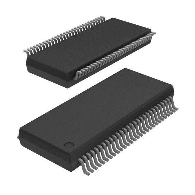
| 供应商器件封装 | 14-SOIC |
| 元件数 | 4 |
| 其它名称 | MM74HC125MXCT |
| 包装 | 剪切带 (CT) |
| 单位重量 | 241 mg |
| 商标 | Fairchild Semiconductor |
| 安装类型 | 表面贴装 |
| 安装风格 | SMD/SMT |
| 封装 | Reel |
| 封装/外壳 | 14-SOIC(0.154",3.90mm 宽) |
| 封装/箱体 | SOIC-14 |
| 工作温度 | -40°C ~ 85°C |
| 工厂包装数量 | 2500 |
| 最大功率耗散 | 500 mW |
| 最大工作温度 | + 85 C |
| 最小工作温度 | - 40 C |
| 极性 | Non-Inverting |
| 标准包装 | 1 |
| 每元件位数 | 1 |
| 每芯片的通道数量 | 4 |
| 电压-电源 | 2 V ~ 6 V |
| 电流-输出高,低 | 7.8mA,7.8mA |
| 电源电压-最大 | 6 V |
| 电源电压-最小 | 2 V |
| 系列 | MM74HC125 |
| 输入线路数量 | 4 |
| 输出类型 | 3-State |
| 输出线路数量 | 1 |
| 逻辑类型 | 缓冲器/线路驱动器,非反相 |
| 逻辑系列 | HC |
| 零件号别名 | MM74HC125MX_NL |
| 高电平输出电流 | - 7.8 mA |


- 商务部:美国ITC正式对集成电路等产品启动337调查
- 曝三星4nm工艺存在良率问题 高通将骁龙8 Gen1或转产台积电
- 太阳诱电将投资9.5亿元在常州建新厂生产MLCC 预计2023年完工
- 英特尔发布欧洲新工厂建设计划 深化IDM 2.0 战略
- 台积电先进制程称霸业界 有大客户加持明年业绩稳了
- 达到5530亿美元!SIA预计今年全球半导体销售额将创下新高
- 英特尔拟将自动驾驶子公司Mobileye上市 估值或超500亿美元
- 三星加码芯片和SET,合并消费电子和移动部门,撤换高东真等 CEO
- 三星电子宣布重大人事变动 还合并消费电子和移动部门
- 海关总署:前11个月进口集成电路产品价值2.52万亿元 增长14.8%


PDF Datasheet 数据手册内容提取
Is Now Part of To learn more about ON Semiconductor, please visit our website at www.onsemi.com Please note: As part of the Fairchild Semiconductor integration, some of the Fairchild orderable part numbers will need to change in order to meet ON Semiconductor’s system requirements. Since the ON Semiconductor product management systems do not have the ability to manage part nomenclature that utilizes an underscore (_), the underscore (_) in the Fairchild part numbers will be changed to a dash (-). This document may contain device numbers with an underscore (_). Please check the ON Semiconductor website to verify the updated device numbers. The most current and up-to-date ordering information can be found at www.onsemi.com. Please email any questions regarding the system integration to Fairchild_questions@onsemi.com. ON Semiconductor and the ON Semiconductor logo are trademarks of Semiconductor Components Industries, LLC dba ON Semiconductor or its subsidiaries in the United States and/or other countries. ON Semiconductor owns the rights to a number of patents, trademarks, copyrights, trade secrets, and other intellectual property. A listing of ON Semiconductor’s product/patent coverage may be accessed at www.onsemi.com/site/pdf/Patent-Marking.pdf. ON Semiconductor reserves the right to make changes without further notice to any products herein. ON Semiconductor makes no warranty, representation or guarantee regarding the suitability of its products for any particular purpose, nor does ON Semiconductor assume any liability arising out of the application or use of any product or circuit, and specifically disclaims any and all liability, including without limitation special, consequential or incidental damages. Buyer is responsible for its products and applications using ON Semiconductor products, including compliance with all laws, regulations and safety requirements or standards, regardless of any support or applications information provided by ON Semiconductor. “Typical” parameters which may be provided in ON Semiconductor data sheets and/or specifications can and do vary in different applications and actual performance may vary over time. All operating parameters, including “Typicals” must be validated for each customer application by customer’s technical experts. ON Semiconductor does not convey any license under its patent rights nor the rights of others. ON Semiconductor products are not designed, intended, or authorized for use as a critical component in life support systems or any FDA Class 3 medical devices or medical devices with a same or similar classification in a foreign jurisdiction or any devices intended for implantation in the human body. Should Buyer purchase or use ON Semiconductor products for any such unintended or unauthorized application, Buyer shall indemnify and hold ON Semiconductor and its officers, employees, subsidiaries, affiliates, and distributors harmless against all claims, costs, damages, and expenses, and reasonable attorney fees arising out of, directly or indirectly, any claim of personal injury or death associated with such unintended or unauthorized use, even if such claim alleges that ON Semiconductor was negligent regarding the design or manufacture of the part. ON Semiconductor is an Equal Opportunity/Affirmative Action Employer. This literature is subject to all applicable copyright laws and is not for resale in any manner.
M M 7 4 February 2008 H C MM74HC125, MM74HC126 1 2 5 3-STATE Quad Buffers , M M 7 Features General Description 4 H C ■ Typical propagation delay: 13ns The MM74HC125 and MM74HC126 are general pur- 1 ■ Wide operating voltage range: 2V–6V pose 3-STATE high speed non-inverting buffers utilizing 2 6 ■ Low input current: 1µA maximum advanced silicon-gate CMOS technology. They have — high drive current outputs which enable high speed oper- ■ Low quiescent current: 80µA maximum (74HC) ation even when driving large bus capacitances. These 3 ■ Fanout of 15 LS-TTL loads circuits possess the low power dissipation of CMOS -S T circuitry, yet have speeds comparable to low power A Schottky TTL circuits. Both circuits are capable of driving T E up to 15 low power Schottky inputs. Q The MM74HC125 require the 3-STATE control input C to u a be taken high to put the output into the high impedance d condition, whereas the MM74HC126 require the control B input to be low to put the output into high impedance. u f f All inputs are protected from damage due to static e r discharge by diodes to V and ground. s CC Ordering Information Package Order Number Number Package Description MM74HC125M M14A 14-Lead Small Outline Integrated Circuit (SOIC), JEDEC MS-012, 0.150" Narrow MM74HC125SJ M14D 14-Lead Small Outline Package (SOP), EIAJ TYPE II, 5.3mm Wide MM74HC125MTC MTC14 14-Lead Thin Shrink Small Outline Package (TSSOP), JEDEC MO-153, 4.4mm Wide MM74HC125N N14A 14-Lead Plastic Dual-In-Line Package (PDIP), JEDEC MS-001, 0.300" Wide MM74HC126M M14A 14-Lead Small Outline Integrated Circuit (SOIC), JEDEC MS-012, 0.150" Narrow MM74HC126SJ M14D 14-Lead Small Outline Package (SOP), EIAJ TYPE II, 5.3mm Wide MM74HC126MTC MTC14 14-Lead Thin Shrink Small Outline Package (TSSOP), JEDEC MO-153, 4.4mm Wide MM74HC126N N14A 14-Lead Plastic Dual-In-Line Package (PDIP), JEDEC MS-001, 0.300" Wide Device also available in Tape and Reel. Specify by appending suffix letter “X” to the ordering number. All packages are lead free per JEDEC: J-STD-020B standard. ©1983 Fairchild Semiconductor Corporation www.fairchildsemi.com MM74HC125, MM74HC126 Rev. 1.3.0
M M Connection Diagrams 7 4 Pin Assignments for DIP, SOIC, SOP and TSSOP H C 1 2 5 , M M 7 4 H C 1 2 6 — 3 - S T A T E Top View (MM74HC125) Top View (MM74HC126) Q u a d Truth Tables B u f Inputs Output Inputs Output fe r A C Y A C Y s H L H H H H L L L L H L X H Z X L Z MM74HC125 MM74HC126 ©1983 Fairchild Semiconductor Corporation www.fairchildsemi.com MM74HC125, MM74HC126 Rev. 1.3.0 2
M M Absolute Maximum Ratings(1) 7 4 Stresses exceeding the absolute maximum ratings may damage the device. The device may not function or be H operable above the recommended operating conditions and stressing the parts to these levels is not recommended. C 1 In addition, extended exposure to stresses above the recommended operating conditions may affect device reliability. 2 The absolute maximum ratings are stress ratings only. 5 , M Symbol Parameter Rating M 7 V Supply Voltage –0.5 to +7.0V CC 4 H V DC Input Voltage –1.5 to V +1.5V IN CC C V DC Output Voltage –0.5 to V +0.5V 1 OUT CC 2 6 IIK, IOK Clamp Diode Current ±20mA — IOUT DC Output Current, per pin 35mA 3 ICC DC VCC or GND Current, per pin ±70mA -S T TSTG Storage Temperature Range –65°C to +150°C A T PD Power Dissipation E Note 2 600mW Q u S.O. Package only 500mW a d TL Lead Temperature (Soldering 10 seconds) 260°C B u Notes: f f 1. Unless otherwise specified all voltages are referenced to ground. e r s 2. Power Dissipation temperature derating — plastic “N” package: –12mW/°C from 65°C to 85°C. Recommended Operating Conditions The Recommended Operating Conditions table defines the conditions for actual device operation. Recommended operating conditions are specified to ensure optimal performance to the datasheet specifications. Fairchild does not recommend exceeding them or designing to absolute maximum ratings. Symbol Parameter Min. Max. Units V Supply Voltage 2 6 V CC V , V DC Input or Output Voltage 0 V V IN OUT CC T Operating Temperature Range –40 +85 °C A t , t Input Rise or Fall Times r f VCC = 2.0V 1000 ns V = 4.5V 500 ns CC V = 6.0V 400 ns CC ©1983 Fairchild Semiconductor Corporation www.fairchildsemi.com MM74HC125, MM74HC126 Rev. 1.3.0 3
M DC Electrical Characteristics(3) M 7 4 T = –40°C T = –40°C H A A C TA = 25°C to 85°C to 125°C 1 2 Symbol Parameter Conditions V (V) Typ. Guaranteed Limits Units 5 CC , M V Minimum HIGH 2.0 1.5 1.5 1.5 V IH M Level Input 4.5 3.15 3.15 3.15 7 Voltage 4 6.0 4.2 4.2 4.2 H C VIL Maximum LOW 2.0 0.5 0.5 0.5 V 1 Level Input 2 4.5 1.35 1.35 1.35 6 Voltage — 6.0 1.8 1.8 1.8 V Minimum HIGH V = V or V , 2.0 2.0 1.9 1.9 1.9 V 3 OH IN IH IL - S Level Output |I | ≤ 20µA OUT 4.5 4.5 4.4 4.4 4.4 T Voltage A 6.0 6.0 5.9 5.9 5.9 T E VIN = VIH or VIL, 4.5 4.2 3.98 3.84 3.7 Q |I | ≤ 6.0mA u OUT a V = V or V , 6.0 5.7 5.48 5.34 5.2 d IN IH IL |I | ≤ 7.8mA B OUT u VOL Maximum LOW VIN = VIH or VIL, 2.0 0 0.1 0.1 0.1 V ffe Level Output |IOUT| ≤ 20µA 4.5 0 0.1 0.1 0.1 rs Voltage 6.0 0 0.1 0.1 0.1 V = V or V , 4.5 0.2 0.26 0.33 0.4 IN IH IL |I | ≤ 6.0mA OUT V = V or V , 6.0 0.2 0.26 0.33 0.4 IN IH IL |I | ≤ 7.8mA OUT I Maximum V = V or V , 6.0 ±0.5 ±5 ±10 µA OZ IN IH IL 3-STATE Output V = V or GND, OUT CC Leakage Current C = Disabled n I Maximum Input V = V or GND 6.0 ±0.1 ±1.0 ±1.0 µA IN IN CC Current I Maximum V = V or GND, 6.0 8.0 80 160 µA CC IN CC Quiescent I = 0µA OUT Supply Current Note: 3. For a power supply of 5V ±10% the worst case output voltages (V , and V ) occur for HC at 4.5V. Thus the 4.5V OH OL values should be used when designing with this supply. Worst case V and V occur at V =5.5V and 4.5V IH IL CC respectively. (The V value at 5.5V is 3.85V.) The worst case leakage current (I , I , and I ) occur for CMOS at IH IN CC OZ the higher voltage and so the 6.0V values should be used. ©1983 Fairchild Semiconductor Corporation www.fairchildsemi.com MM74HC125, MM74HC126 Rev. 1.3.0 4
M M AC Electrical Characteristics 7 V = 5V, T = 25°C, C = 45pF, t = t = 6ns 4 CC A L r f H C Guaranteed 1 Symbol Parameter Conditions Typ. Limit Units 2 5 tPHL, tPLH Maximum Propagation Delay Time 13 18 ns , M t Maximum Output Enable Time to HIGH R = 1kΩ 13 25 ns M PZH L 7 Level 4 H t Maximum Output Disable Time from R = 1kΩ, C = 5pF 17 25 ns PHZ L L C HIGH Level 1 2 t Maximum Output Enable Time to LOW R = 1kΩ 18 25 ns 6 PZL L Level — t Maximum Output Disable Time from R = 1kΩ, C = 5pF 13 25 ns 3 PLZ L L - LOW Level S T A T E AC Electrical Characteristics Q V = 2.0V to 6.0V, C = 50pF, t = t = 6ns (unless otherwise specified) u CC L r f a d TA = –40°C TA = –40°C B TA = 25°C to 85°C to 125°C u f Symbol Parameter VCC (V) Conditions Typ. Guaranteed Limits Units fe r s t , t Maximum Propagation 2.0 40 100 125 150 ns PHL PLH Delay Time 4.5 14 20 25 30 6.0 12 17 21 25 t , t Maximum Propagation 2.0 C = 150pF 35 130 163 195 ns PLH PHL L Delay Time 4.5 14 26 33 39 6.0 12 22 28 39 t , t Maximum Output 2.0 R = 1kΩ 25 125 156 188 ns PZH PZL L Enable Time 4.5 14 25 31 38 6.0 12 21 26 31 t , t Maximum Output 2.0 R = 1kΩ 25 125 156 188 ns PHZ PLZ L Disable Time 4.5 14 25 31 38 6.0 12 21 26 31 t , t Maximum Output 2.0 C = 150pF, 35 140 175 210 ns PZL PZH L Enable Time 4.5 RL = 1kΩ 15 28 35 42 6.0 13 24 30 36 t , t Maximum Output 2.0V C = 50pF 30 60 75 90 ns TLH THL L Rise and Fall Time 4.5V 7 12 15 18 6.0V 6 10 13 15 C Input Capacitance 5 10 10 10 pF IN C Output Capacitance 15 20 20 20 pF OUT Outputs C Power Dissipation Enabled 45 pF PD Capacitance Disabled 6 (per gate)(4) Note: 4. C determines the no load dynamic power consumption, P = C V 2f + I V , and the no load dynamic PD D PD CC CC CC current consumption, I = C V f + I . S PD CC CC ©1983 Fairchild Semiconductor Corporation www.fairchildsemi.com MM74HC125, MM74HC126 Rev. 1.3.0 5
0.65 (cid:24)(cid:17)(cid:19)(cid:19)(cid:147)(cid:19)(cid:17)(cid:20)(cid:19) A 0.43TYP 14 8 B 6.4 (cid:23)(cid:17)(cid:23)(cid:19)(cid:147)(cid:19)(cid:17)(cid:20)(cid:19) 6.10 3.2 1.65 1 7 0.2 C B A PIN1IDENT TOPVIEW ALLLEADTIPS 0.45 RECOMMENDEDLANDPATTERN 1.2MAX SEEDETAILA +0.15 0.90 -0.10 0.20 (cid:19)(cid:17)(cid:20)(cid:19)(cid:147)(cid:19)(cid:17)(cid:19)(cid:24) 0.09 ALLLEADTIPS 0.30 0.19 C 0.1 C 0.65 0.13 A B C (cid:20)(cid:21)(cid:17)(cid:19)(cid:19)(cid:131)(cid:3)(cid:55)(cid:50)(cid:51)(cid:3)(cid:9)(cid:3)(cid:37)(cid:50)(cid:55)(cid:55)(cid:50)(cid:48) FRONTVIEW 0.09MIN NOTES: GAGEPLANE A.CONFORMSTOJEDECREGISTRATIONMO-153, VARIATIONAB,REFNOTE6 B.DIMENSIONSAREINMILLIMETERS. 0.25 0.09MIN C.DIMENSIONSAREEXCLUSIVEOFBURRS, (cid:19)(cid:131)(cid:16)(cid:3)(cid:27)(cid:131) (cid:19)(cid:17)(cid:25)(cid:147)(cid:19)(cid:17)(cid:20) MOLDFLASH,ANDTIEBAREXTRUSIONS SEATINGPLANE 1.00 D.DIMENSIONINGANDTOLERANCESPERANSI DETAILA Y14.5M,2009. E.LANDPATTERNSTANDARD:SOP65P640X110-14M. F.DRAWINGFILENAME:MKT-MTC14rev7.
8.75 A 8.50 7.62 14 0.65 8 14 8 B 4.00 6.00 5.60 3.80 1.70 1 7 PIN #1 1.27 0.51 1 7 IDENT. 1.27 0.35 (0.33) 0.25 M C B A LAND PATTERN RECOMMENDATION TOP VIEW 1.75 MAX A C 0.25 0.19 1.50 0.10 C 0.25 1.25 0.10 SIDE VIEW FRONT VIEW NOTES: A. CONFORMS TO JEDEC MS-012, VARIATION AB, ISSUE C B. ALL DIMENSIONS ARE IN MILLIMETERS 0.50 0.25 x 45 C. DIMENSIONS DO NOT INCLUDE MOLD FLASH OR BURRS R0.10 GAGE D. LAND PATTERN STANDARD: PLANE SOIC127P600X145-14M R0.10 E. CONFORMS TO ASME Y14.5M, 2009 0.36 D. DRAWING FILENAME: MKT-M14Arev14 8° 0° 0.90 0.50 SEATING PLANE (1.04) DETAIL A SCALE 16 : 1
ON Semiconductor and are trademarks of Semiconductor Components Industries, LLC dba ON Semiconductor or its subsidiaries in the United States and/or other countries. ON Semiconductor owns the rights to a number of patents, trademarks, copyrights, trade secrets, and other intellectual property. A listing of ON Semiconductor’s product/patent coverage may be accessed at www.onsemi.com/site/pdf/Patent−Marking.pdf. ON Semiconductor reserves the right to make changes without further notice to any products herein. ON Semiconductor makes no warranty, representation or guarantee regarding the suitability of its products for any particular purpose, nor does ON Semiconductor assume any liability arising out of the application or use of any product or circuit, and specifically disclaims any and all liability, including without limitation special, consequential or incidental damages. Buyer is responsible for its products and applications using ON Semiconductor products, including compliance with all laws, regulations and safety requirements or standards, regardless of any support or applications information provided by ON Semiconductor. “Typical” parameters which may be provided in ON Semiconductor data sheets and/or specifications can and do vary in different applications and actual performance may vary over time. All operating parameters, including “Typicals” must be validated for each customer application by customer’s technical experts. ON Semiconductor does not convey any license under its patent rights nor the rights of others. ON Semiconductor products are not designed, intended, or authorized for use as a critical component in life support systems or any FDA Class 3 medical devices or medical devices with a same or similar classification in a foreign jurisdiction or any devices intended for implantation in the human body. Should Buyer purchase or use ON Semiconductor products for any such unintended or unauthorized application, Buyer shall indemnify and hold ON Semiconductor and its officers, employees, subsidiaries, affiliates, and distributors harmless against all claims, costs, damages, and expenses, and reasonable attorney fees arising out of, directly or indirectly, any claim of personal injury or death associated with such unintended or unauthorized use, even if such claim alleges that ON Semiconductor was negligent regarding the design or manufacture of the part. ON Semiconductor is an Equal Opportunity/Affirmative Action Employer. This literature is subject to all applicable copyright laws and is not for resale in any manner. PUBLICATION ORDERING INFORMATION LITERATURE FULFILLMENT: N. American Technical Support: 800−282−9855 Toll Free ON Semiconductor Website: www.onsemi.com Literature Distribution Center for ON Semiconductor USA/Canada 19521 E. 32nd Pkwy, Aurora, Colorado 80011 USA Europe, Middle East and Africa Technical Support: Order Literature: http://www.onsemi.com/orderlit Phone: 303−675−2175 or 800−344−3860 Toll Free USA/Canada Phone: 421 33 790 2910 Fax: 303−675−2176 or 800−344−3867 Toll Free USA/Canada Japan Customer Focus Center For additional information, please contact your local Email: orderlit@onsemi.com Phone: 81−3−5817−1050 Sales Representative © Semiconductor Components Industries, LLC www.onsemi.com www.onsemi.com 1
Mouser Electronics Authorized Distributor Click to View Pricing, Inventory, Delivery & Lifecycle Information: O N Semiconductor: MM74HC125M MM74HC125SJ MM74HC125MTC MM74HC125MTCX MM74HC125SJX MM74HC125N MM74HC125MX