ICGOO在线商城 > 集成电路(IC) > 嵌入式 - 微控制器 > MINI52LAN
 Datasheet下载
- 型号: MINI52LAN
- 制造商: Nuvoton Technology Corporation of America
- 库位|库存: xxxx|xxxx
- 要求:
| 数量阶梯 | 香港交货 | 国内含税 |
| +xxxx | $xxxx | ¥xxxx |
查看当月历史价格
查看今年历史价格
MINI52LAN产品简介:
ICGOO电子元器件商城为您提供MINI52LAN由Nuvoton Technology Corporation of America设计生产,在icgoo商城现货销售,并且可以通过原厂、代理商等渠道进行代购。 MINI52LAN价格参考。Nuvoton Technology Corporation of AmericaMINI52LAN封装/规格:嵌入式 - 微控制器, ARM® Cortex®-M0 微控制器 IC NuMicro Mini51™ 32-位 24MHz 8KB(8K x 8) 闪存 。您可以下载MINI52LAN参考资料、Datasheet数据手册功能说明书,资料中有MINI52LAN 详细功能的应用电路图电压和使用方法及教程。
Nuvoton Technology Corporation of America(新唐科技北美公司)的嵌入式微控制器型号MINI52LAN,主要应用于以下场景:

1. 工业自动化:MINI52LAN适用于工业控制设备,如传感器数据采集、电机控制和工厂自动化系统。其高性能处理能力和丰富的外设接口能够满足工业环境中对实时性和可靠性的要求。

2. 智能家居:该微控制器可用于智能家居设备,例如智能照明、智能插座和环境监控设备。其低功耗特性和网络连接能力使其适合于需要长时间运行且与互联网交互的家用设备。

3. 消费电子:在消费类电子产品中,MINI52LAN可以用于音频设备、家用电器和便携式电子产品。其集成的外设减少了外部组件的需求,降低了系统成本并提高了设计灵活性。

4. 物联网(IoT)设备:凭借其内置的通信协议支持和高效的数据处理能力,MINI52LAN非常适合用于物联网节点设备,如环境监测器、健康追踪器和智能标签等。

5. 医疗设备:在便携式医疗设备中,如血糖仪、脉搏血氧仪和心率监测器,MINI52LAN提供精确的数据处理和低功耗操作,确保设备的准确性和续航能力。

6. 汽车电子:虽然主要用于一般嵌入式应用,但MINI52LAN也可以应用于简单的汽车电子模块,如车内环境控制和诊断工具,因其具备一定的抗干扰能力和稳定性。

综上所述,MINI52LAN以其高效的性能、灵活的设计和多样的功能,在多个领域都有广泛的应用潜力,特别适合需要嵌入式计算能力和网络连接的场景。
| 参数 | 数值 |
| 产品目录 | 集成电路 (IC) |
| 描述 | IC MCU 32BIT 8KB FLASH 48LQFP |
| EEPROM容量 | - |
| 产品分类 | |
| I/O数 | 30 |
| 品牌 | Nuvoton Technology Corporation of America |
| 数据手册 | |
| 产品图片 |
|
| 产品型号 | MINI52LAN |
| RAM容量 | 2K x 8 |
| rohs | 无铅 / 符合限制有害物质指令(RoHS)规范要求 |
| 产品系列 | NuMicro Mini51™ |
| 供应商器件封装 | * |
| 包装 | 托盘 |
| 外设 | 欠压检测/复位,POR,PWM,WDT |
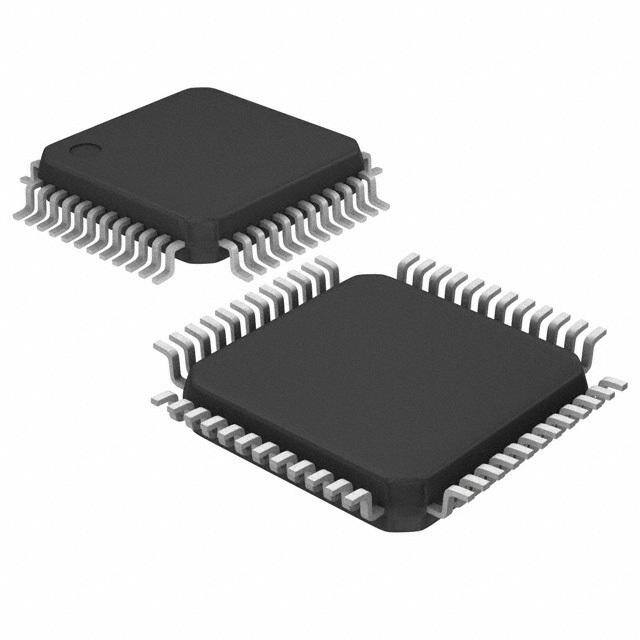
| 封装/外壳 | 48-LQFP |
| 工作温度 | -40°C ~ 85°C |
| 振荡器类型 | 内部 |
| 数据转换器 | A/D 8x10b |
| 标准包装 | 250 |
| 核心处理器 | ARM® Cortex™-M0 |
| 核心尺寸 | 32-位 |
| 电压-电源(Vcc/Vdd) | 2.5 V ~ 5.5 V |
| 程序存储器类型 | 闪存 |
| 程序存储容量 | 8KB(8K x 8) |
| 连接性 | I²C, IrDA, SPI, UART/USART |
| 速度 | 24MHz |


PDF Datasheet 数据手册内容提取
NuMicro™ Mini51 Series Data Sheet ARM Cortex™-M0 32-BIT MICROCONTROLLER NuMicro™ Family Mini51 Series DataSheet The information described in this document is the exclusive intellectual property of Nuvoton Technology Corporation and shall not be reproduced without permission from Nuvoton. N U M Nuvoton is providing this document only for reference purposes of NuMicro microcontroller based system IC design. Nuvoton assumes no responsibility for errors or omissions. R O ™ All data and specifications are subject to change without notice. M IN For additional information or questions, please contact: Nuvoton Technology Corporation. I5 1 S www.nuvoton.com E R IE S D A T A S H E E T
NuMicro™ Mini51 Series Data Sheet T CONTENTS E E 1 GENERAL DESCRIPTION ..................................................................................................... 7 H S 2 FEATURES ............................................................................................................................. 8 A T A 3 PARTS INFORMATION LIST AND PIN CONFIGURATION ................................................ 11 D S 3.1 NuMicro Mini51 Series Product Selection Guide .................................................... 11 E RI 3.2 PIN CONFIGURATION .............................................................................................. 12 E S 3.2.1 LQFP 48-pin ................................................................................................................... 12 1 5 3.2.2 QFN 33-pin ..................................................................................................................... 13 NI MI 3.3 Pin Description ........................................................................................................... 14 ™ 4 BLOCK DIAGRAM ................................................................................................................ 18 O 4.1 NuMicro Mini51™ Block Diagram .............................................................................. 18 R C MI 5 FUNCTIONAL DESCRIPTION.............................................................................................. 19 U 5.1 Memory Organization ................................................................................................. 19 N 5.1.1 Overview ........................................................................................................................ 19 5.1.2 System Memory Map...................................................................................................... 20 5.2 Nested Vectored Interrupt Controller (NVIC) ............................................................. 21 5.2.1 Overview ........................................................................................................................ 21 5.2.2 Features ......................................................................................................................... 21 5.2.3 Exception Model and System Interrupt Map ................................................................... 21 5.2.4 Vector Table ................................................................................................................... 23 5.2.5 NVIC Operation .............................................................................................................. 24 5.3 System Manager ........................................................................................................ 25 5.3.1 Overview ........................................................................................................................ 25 5.3.2 System Reset ................................................................................................................. 25 5.3.3 System Power Distribution ............................................................................................. 25 5.3.4 Memory Mapping Table .................................................................................................. 27 5.4 Clock Controller .......................................................................................................... 28 5.4.1 Overview ........................................................................................................................ 28 5.4.2 Clock Generator ............................................................................................................. 28 5.4.3 System Clock and SysTick Clock ................................................................................... 29 5.4.4 AHB Clock Source Selection .......................................................................................... 30 5.4.5 Peripheral Clock Source Selection ................................................................................. 31 5.4.6 Power-down Mode Clock ................................................................................................ 33 5.4.7 Frequency Divider Output ............................................................................................... 34 5.5 Comparator Controller (CMPC) .................................................................................. 35 5.5.1 Overview ........................................................................................................................ 35 5.5.2 Features ......................................................................................................................... 35 5.6 Analog-to-Digital Converter (ADC) ............................................................................. 36 5.6.1 Overview ........................................................................................................................ 36 5.6.2 Features ......................................................................................................................... 36 5.7 Flash Memory Controller (FMC) ................................................................................. 37 5.7.1 Overview ........................................................................................................................ 37 5.7.2 Features ......................................................................................................................... 37 Feb 9, 2012 Page 2 of 68 Revision V1.03
NuMicro™ Mini51 Series Data Sheet 5.8 General Purpose I/O .................................................................................................. 38 5.8.1 Overview ........................................................................................................................ 38 5.8.2 Features ......................................................................................................................... 38 5.9 I2C Serial Interface Controller (Master/Slave) ............................................................ 39 5.9.1 Overview ........................................................................................................................ 39 5.9.2 Features ......................................................................................................................... 39 5.10 Enhanced PWM Generator ........................................................................................ 41 5.10.1 Overview ...................................................................................................................... 41 5.10.2 Features ....................................................................................................................... 41 5.11 Serial Peripheral Interface (SPI) Controller ................................................................ 43 5.11.1 Overview ...................................................................................................................... 43 5.11.2 Features ....................................................................................................................... 43 5.12 Timer Controller .......................................................................................................... 44 5.12.1 Overview ...................................................................................................................... 44 5.12.2 Features ....................................................................................................................... 44 5.13 UART Interface Controller .......................................................................................... 45 5.13.1 Overview ...................................................................................................................... 45 5.13.2 Features ....................................................................................................................... 47 5.14 Watchdog Timer ......................................................................................................... 48 5.14.1 Overview ...................................................................................................................... 48 5.14.2 Features ....................................................................................................................... 49 6 ARM® CORTEX™-M0 CORE ............................................................................................... 50 6.1 Overview .................................................................................................................... 50 6.2 Features ..................................................................................................................... 51 7 APPLICATION CIRCUIT ....................................................................................................... 52 8 ELECTRICAL CHARACTERISTICS ..................................................................................... 53 8.1 Absolute Maximum Ratings ....................................................................................... 53 8.2 DC Electrical Characteristics ...................................................................................... 54 8.3 AC Electrical Characteristics ...................................................................................... 59 N U 8.3.1 External Input Clock ....................................................................................................... 59 M IC 8.3.2 External 4 ~ 24 MHz XTAL Oscillator ............................................................................. 59 R 8.3.3 Typical Crystal Application Circuit .................................................................................. 59 O ™ 8.3.4 External 32.768 KHz XTAL Oscillator ............................................................................. 60 M 8.3.5 Internal 22.1184 MHz RC Oscillator ............................................................................... 60 IN 8.3.6 Internal 10 KHz RC Oscillator ......................................................................................... 60 I5 1 8.4 Analog Characteristics ............................................................................................... 61 S E 8.4.1 Brown-Out Reset (BOD) ................................................................................................. 61 R IE 8.4.2 Low Voltage Reset (LVR) ............................................................................................... 61 S 8.4.3 Analog Comparator ........................................................................................................ 61 D A 8.4.4 Analog Comparator Reference Voltage (CRV) ............................................................... 62 TA 8.4.5 10-bit ADC ...................................................................................................................... 62 SH 8.4.6 Flash Memory Characteristics ........................................................................................ 63 E E 9 PACKAGE DIMENSION ....................................................................................................... 64 T Feb 9, 2012 Page 3 of 68 Revision V1.03
NuMicro™ Mini51 Series Data Sheet T 9.1 48-pin LQFP ............................................................................................................... 64 E E 9.2 33-pin QFN (4mm x 4mm) ......................................................................................... 65 H S A 9.3 33-pin QFN (5mm x 5mm) ......................................................................................... 66 T A 10 REVISION HISTORY ............................................................................................................ 67 D S E RI E S 1 5 NI MI ™ O R C MI U N Feb 9, 2012 Page 4 of 68 Revision V1.03
NuMicro™ Mini51 Series Data Sheet List of Figures Figure 3.1-1 NuMicro Mini51 Series Product Selection Guide .................................................... 11 Figure 3.2-1 NuMicro Mini51 Series LQFP 48-pin Assignment .................................................. 12 Figure 3.2-2 NuMicro Mini51 Series QFN 33-pin Assignment .................................................... 13 Figure 4.1-1 NuMicro Mini51 Series Block Diagram ................................................................... 18 Figure 5.3-1 NuMicro Mini51 Series Power Distribution Diagram............................................... 26 Figure 5.4-1 Clock Generator Block Diagram ................................................................................ 28 Figure 5.4-2 System Clock Block Diagram .................................................................................... 29 Figure 5.4-3 SysTick Clock Control Block Diagram ....................................................................... 29 Figure 5.4-4 AHB Clock Source for HCLK ..................................................................................... 30 Figure 5.4-5 Peripherals Clock Source Selection for PCLK .......................................................... 31 Figure 5.4-6 Clock Source of Frequency Divider ........................................................................... 34 Figure 5.4-7 Block Diagram of Frequency Divider ......................................................................... 34 Figure 5.9-1 Bus Timing ................................................................................................................. 39 Figure 5.10-1 Application Circuit Diagram ..................................................................................... 42 Figure 5.14-1 Timing of Interrupt and Reset Signal ....................................................................... 49 Figure 6.1-1 Functional Block Diagram .......................................................................................... 50 Figure 8.3-1 Typical Crystal Application Circuit ............................................................................. 60 N U M IC R O ™ M IN I5 1 S E R IE S D A T A S H E E T Feb 9, 2012 Page 5 of 68 Revision V1.03
NuMicro™ Mini51 Series Data Sheet T List of Tables E E H Table 3.3-1 NuMicro Mini51 Series Pin Description ................................................................... 17 S A Table 5.1-1 Address Space Assignments for On-Chip Modules ................................................... 20 T A D Table 5.2-1 Exception Model ......................................................................................................... 22 S E Table 5.2-2 System Interrupt Map ................................................................................................. 23 RI E Table 5.2-3 Vector Table Format ................................................................................................... 23 S 1 5 Table 5.3-1 Memory Mapping Table .............................................................................................. 27 NI MI Table 5.4-1 Peripherals Engine Clock Source Selection Table ..................................................... 32 ™ Table 5.13-1 UART Baud Rate Setting Table ................................................................................ 45 O R Table 5.13-2 UART Baud Rate Setting Table ................................................................................ 45 C MI Table 5.14-1 Watchdog Time-out Interval Selection ...................................................................... 48 U N Feb 9, 2012 Page 6 of 68 Revision V1.03
NuMicro™ Mini51 Series Data Sheet 1 GENERAL DESCRIPTION The NuMicro Mini51™ series 32-bit microcontroller is embedded with an ARM® Cortex™-M0 core for industrial controls and applications which require high performance, high integration, and low cost. The Cortex™-M0 is the newest ARM embedded processor with 32-bit performance at a cost equivalent to the traditional 8-bit microcontroller. The NuMicro Mini51™ series can run up to 24 MHz, and thus can afford to support a variety of industrial controls and applications requiring high CPU performance. The NuMicro Mini51™ series provides 4K/8K/16K-byte embedded program flash, size configurable data flash (shared with program flash), 2K-byte flash for the ISP, and 2K-byte embedded SRAM. A number of system-level peripheral functions, such as I/O Port, Timer, UART, SPI, I2C, PWM, ADC, Watchdog Timer, and low voltage detector, have been incorporated in the NuMicro Mini51™ series to reduce component count, board space, and system cost. These useful functions make the NuMicro Mini51™ series powerful for a wide range of applications. Additionally, the NuMicro Mini51™ series is equipped with ISP (In-System Programming) and ICP (In-Circuit Programming) functions, allowing user to update program memory without removing a chip from an actual end product. N U M IC R O ™ M IN I5 1 S E R IE S D A T A S H E E T Feb 9, 2012 Page 7 of 68 Revision V1.03
NuMicro™ Mini51 Series Data Sheet T 2 FEATURES E E H Core S A ARM® Cortex™-M0 core running up to 24 MHz T A D One 24-bit system timer S E Supports low power Idle mode RI E A single-cycle 32-bit hardware multiplier S 1 5 NVIC for 32 interrupt inputs, each with 4-level priority NI MI Supports Serial Wire Debug (SWD) with 2 watchpoints/4 breakpoints ™ Built-in LDO for Wide Operating Voltage Range: 2.5V to 5.5V O R Memory C MI 4KB/8KB/16KB flash memory for program memory (APROM) U N Configurable flash memory for data memory (Data Flash) 2KB flash memory for loader (LDROM) 2KB SRAM for internal scratch-pad RAM (SRAM) In-System Programming (ISP) and In-Circuit Programming (ICP) Clock Control Programmable system clock source Switch clock sources on-the-fly 4 ~ 24 MHz crystal oscillator (HXT) 32.768K crystal oscillator (LXT) for idle wake-up and system operation clock 22.1184 MHz internal oscillator (HIRC) (1% accuracy at 250C, 5V) Dynamically calibrating the HIRC OSC to 22.0 MHz ±1% from -400C to 850C by external 32.768K crystal oscillator (LXT) 10 KHz internal low-power oscillator (LIRC) for watchdog and idle wake-up I/O Port Up to 30 GPIO (General Purpose I/O) pins for LQFP-48 package Software-configured I/O type Quasi-bidirectional input/output Push-pull output Open-drain output Input-only (high impendence) Optional Schmitt trigger input Timer Two 24-bit Timers with 8-bit prescaler Supports Event Counter mode Supports Toggle Output mode Feb 9, 2012 Page 8 of 68 Revision V1.03
NuMicro™ Mini51 Series Data Sheet Supports external trigger in Pulse Width Measurement mode Supports external trigger in Pulse Width Capture mode Watchdog Timer Programmable clock source and time-out period Supports wake-up function in Power-down mode and Idle mode Interrupt or reset selectable when time-out happens PWM Up to three built-in 16-bit PWM generators with six PWM outputs or three complementary paired PWM outputs Supports edge alignment or center alignment Supports fault detection Individual clock source, clock divider, 8-bit prescalar and dead-zone generator for each PWM generator PWM interrupt synchronized to PWM period UART (Universal Asynchronous Receiver/Transmitters) One UART device Buffered receiver and transmitter with 16-byte FIFO Optional flow control function (CTSn and RTSn) Supports IrDA (SIR) function Programmable baud-rate generator up to 1/16 system clock Supports RS-485 function SPI (Serial Peripheral Interface) One SPI device Masters up to 12 MHz, and Slaves up to 4 MHz Supports SPI Master/Slave mode Full duplex synchronous serial data transfer N U M Variable length of transfer data from 1 to 32 bits IC R MSB or LSB first data transfer O ™ Rx and Tx on both rising or falling edge of serial clock independently M Byte Suspend mode in 32-bit transmission IN I5 I2C 1 S Supports Master/Slave mode E R IE Bi-directional data transfer between masters and slaves S D Multi-master bus (no central master) A T Arbitration between simultaneously transmitting masters without corruption of A S serial data on the bus H E E Serial clock synchronization allowing devices with different bit rates to T communicate via one serial bus Feb 9, 2012 Page 9 of 68 Revision V1.03
NuMicro™ Mini51 Series Data Sheet T Serial clock synchronization used as a handshake mechanism to suspend and E resume serial transfer E H S Programmable clocks allowing for versatile rate control A T Supports multiple address recognition (4 slave addresses with mask option) A D S ADC (Analog-to-Digital Converter) E RI 10-bit SAR ADC with 150K SPS E S Up to 8-ch single-end input and one internal input from band-gap 1 5 NI Conversion started by software or external pin MI Analog Comparator ™ O Two analog comparators with programmable 16-level internal voltage reference R C Built-in CRV (comparator reference voltage) MI U BOD (Brown-Out Detection) Reset N Three programmable threshold levels: 3.8V/2.7V/2.0V (default as 2.0V) Optional BOD interrupt or reset 96-bit unique ID Operating Temperature: -40℃~85℃ Packages: Green package (RoHS) LQFP 48-pin (7x7), QFN 33-pin (5x5), QFN 33-pin (4x4) Feb 9, 2012 Page 10 of 68 Revision V1.03
NuMicro™ Mini51 Series Data Sheet 3 PARTS INFORMATION LIST AND PIN CONFIGURATION 3.1 NuMicro Mini51 Series Product Selection Guide ISP Connectivity IRC ISP Part Number APROM RAM Data Flash Loader I/O Timer Comp. PWM ADC 22.1184 Package ICP ROM UART SPI I2C MHz MINI51LAN 4 KB 2 KB Configurable 2 KB up to 30 2x32-bit 1 1 1 2 6 8x10-bit v v LQFP48 MINI51ZAN 4 KB 2 KB Configurable 2 KB up to 29 2x32-bit 1 1 1 2 6 8x10-bit v v QFN33(5x5) MINI51TAN 4 KB 2 KB Configurable 2 KB up to 29 2x32-bit 1 1 1 2 6 8x10-bit v v QFN33(4x4) MINI52LAN 8 KB 2 KB Configurable 2 KB up to 30 2x32-bit 1 1 1 2 6 8x10-bit v v LQFP48 MINI52ZAN 8 KB 2 KB Configurable 2 KB up to 29 2x32-bit 1 1 1 2 6 8x10-bit v v QFN33(5x5) MINI52TAN 8 KB 2 KB Configurable 2 KB up to 29 2x32-bit 1 1 1 2 6 8x10-bit v v QFN33(4x4) MINI54LAN 16 KB 2 KB Configurable 2 KB up to 30 2x32-bit 1 1 1 2 6 8x10-bit v v LQFP48 MINI54ZAN 16 KB 2 KB Configurable 2 KB up to 29 2x32-bit 1 1 1 2 6 8x10-bit v v QFN33(5x5) MINI54TAN 16 KB 2 KB Configurable 2 KB up to 29 2x32-bit 1 1 1 2 6 8x10-bit v v QFN33(4x4) Figure 3.1-1 NuMicro Mini51 Series Product Selection Guide N U M IC R O ™ M IN I5 1 S E R IE S D A T A S H E E T Feb 9, 2012 Page 11 of 68 Revision V1.03
NuMicro™ Mini51 Series Data Sheet T 3.2 PIN CONFIGURATION E E H S 3.2.1 LQFP 48-pin A T A D S S PIS 51 SERIE CPN0,AIN4,P TX ,AIN3,P RX ,AIN2, P AIN1,P AV V AIN0,P TX, CTSn, P S, RX, RTSn, P NI NC 1.4 1.3 1.2 1.0 DD DD 5.3 NC NC 0.0 0.1 MI ™ 48 47 46 45 44 43 42 41 40 39 38 37 O NC 1 36 NC R C CPP0, AIN5, P1.5 2 35 P0.4, SPISS,PWM5 MI U /RESET 3 34 P0.5, MOSI N CPN1, AIN6, P3.0 4 33 P0.6, MISO AVSS 5 32 P0.7, SPICLK P5.4 6 Mini51 31 NC LQFP 48-pin CPP1, AIN7, P3.1 7 30 P4.7, ICE_DAT T0EX, STADC, INT0, P3.2 8 29 P4.6, ICE_CLK SDA, T0, P3.4 9 28 NC SCL, T1, P3.5 10 27 NC NC 11 26 P2.6, PWM4, CPO1 NC 12 25 P2.5, PWM3 1 1 1 1 1 1 1 2 2 2 2 2 3 4 5 6 7 8 9 0 1 2 3 4 N P P P V L P P N P P P C 3.6 5.1 5.0 SS DO 5.5 5.2 C 2.2 2.3 2.4 , CKO,T ,XTAL2 ,XTAL1 _CAP , INT1 , PWM0 , PWM1 , PWM2 1 E X ,C P O 0 Figure 3.2-1 NuMicro Mini51 Series LQFP 48-pin Assignment Feb 9, 2012 Page 12 of 68 Revision V1.03
NuMicro™ Mini51 Series Data Sheet 3.2.2 QFN 33-pin S P IS C S PN TX RX TX ,RX 0,AIN , AIN , AIN AIN AIN ,CTS ,RTS 4, P 3, P 2, P 1, P V 0,P n, P n, P 1 1 1 1 D 5 0 0 .4 .3 .2 .0 D .3 .0 .1 32 31 30 29 28 27 26 25 CPP0,AIN5, P1.5 1 24 P0.4, SPISS,PWM5 /RESET 2 23 P0.5, MOSI CPN1,AIN6, P3.0 3 22 P0.6, MISO P5.4 4 Mini51 21 P0.7, SPICLK QFN 33-pin CPP1,AIN7, P3.1 5 20 P4.7, ICE_DAT T0EX,STADC,INT0, P3.2 6 19 P4.6, ICE_CLK SDA, T0, P3.4 7 18 P2.6, PWM4,CPO1 33 VSS SCL, T1, P3.5 8 17 P2.5, PWM3 9 10 11 12 13 14 15 16 P P P V P P P P 3 5 5 S 5 2 2 2 .6 .1 .0 S .2 .2 .3 .4 , C ,X ,X ,IN , P , P , P KO TAL TAL T1 WM WM WM ,T 2 1 0 1 2 1 E X ,C top transparent view P O 0 N U M Figure 3.2-2 NuMicro Mini51 Series QFN 33-pin Assignment IC R O ™ M IN I5 1 S E R IE S D A T A S H E E T Feb 9, 2012 Page 13 of 68 Revision V1.03
NuMicro™ Mini51 Series Data Sheet T 3.3 Pin Description E E H Pin Number S A T LQFP QFN Pin Name Pin Type Description A D 48-pin 33-pin S E RI 1 NC Not connected E S P1.5 I/O Digital GPIO pin 1 5 NI 2 1 AIN5 AI ADC analog input pin MI ™ CPP0 AI Analog comparator Positive input pin O The Schmitt trigger input pin for hardware device reset. A R “Low” on this pin for 768 clock counter of Internal RC C MI 3 2 /RESET I(ST) 22.1184 MHz while the system clock is running will reset the U device. /RESET pin has an internal pull-up resistor allowing N power-on reset by simply connecting an external capacitor to GND. P3.0 I/O Digital GPIO pin 4 3 AIN6 AI ADC analog input pin CPN1 AI Analog comparator negative input pin 5 AVSS AP Ground pin for analog circuit 6 4 P5.4 I/O Digital GPIO pin P3.1 I/O Digital GPIO pin 7 5 AIN7 AI ADC analog input pin CPP1 AI Analog comparator positive input pin P3.2 I/O Digital GPIO pin INT0 I External interrupt 0 input pin 8 6 STADC I ADC external trigger input pin T0EX I Timer 0 external capture/reset trigger input pin P3.4 I/O Digital GPIO pin 9 7 T0 I/O Timer 0 external event counter input pin SDA I/O I2C data I/O pin P3.5 I/O Digital GPIO pin 10 8 T1 I/O Timer 1 external event counter input pin SCL I/O I2C clock I/O pin 11 NC Not connected 12 NC Not connected 13 NC Not connected Feb 9, 2012 Page 14 of 68 Revision V1.03
NuMicro™ Mini51 Series Data Sheet Pin Number Pin Name Pin Type Description LQFP QFN 48-pin 33-pin P3.6 I/O Digital GPIO pin CPO0 O Analog comparator output pin 14 9 CKO O Frequency divider output pin T1EX I Timer 1 external capture/reset trigger input pin P5.1 I/O Digital GPIO pin 15 10 The output pin from the internal inverting amplifier. It emits XTAL2 O the inverted signal of XTAL1. P5.0 I/O Digital GPIO pin 16 11 The input pin to the internal inverting amplifier. The system XTAL1 I clock could be from external crystal or resonator. 12 17 VSS P Ground pin for digital circuit 33 LDO_CA 18 P LDO output pin P Digital GPIO pin 19 P5.5 I/O User program must enable pull-up resistor in the QFN-33 package. P5.2 I/O Digital GPIO pin 20 13 INT1 I External interrupt 1 input pin 21 NC Not connected P2.2 I/O Digital GPIO pin 22 14 PWM0 O PWM0 output of PWM unit N U P2.3 I/O Digital GPIO pin M 23 15 IC R PWM1 O PWM1 output of PWM unit O ™ 24 16 P2.4 I/O Digital GPIO pin M PWM2 O PWM2 output of PWM unit IN I5 1 P2.5 I/O Digital GPIO pin S 25 17 E PWM3 O PWM3 output of PWM unit R IE S P2.6 I/O Digital GPIO pin D A 26 18 PWM4 O PWM4 output of PWM unit T A S CPO1 O Analog comparator output pin H E E 27 NC Not connected T Feb 9, 2012 Page 15 of 68 Revision V1.03
NuMicro™ Mini51 Series Data Sheet T Pin Number E E Pin Name Pin Type Description H LQFP QFN S A 48-pin 33-pin T A D 28 NC Not connected S E P4.6 I/O Digital GPIO pin RI 29 19 E S ICE_CLK I Serial wired debugger clock pin 1 5 P4.7 I/O Digital GPIO pin NI 30 20 MI ICE_DAT I/O Serial wired debugger data pin ™ O 31 NC Not connected R C P0.7 I/O Digital GPIO pin MI 32 21 U SPICLK I/O SPI serial clock pin N P0.6 I/O Digital GPIO pin 33 22 MISO I/O SPI MISO (master in/slave out) pin P0.5 I/O Digital GPIO pin 34 23 MOSI O SPI MOSI (master out/slave in) pin P0.4 I/O Digital GPIO pin 35 24 SPISS I/O SPI slave select pin PWM5 O PWM5 output of PWM unit 36 NC Not connected P0.1 I/O Digital GPIO pin RTSn O UART RTS pin 37 25 RX I UART data receiver input pin SPISS I/O SPI slave select pin P0.0 I/O Digital GPIO pin 38 26 CTSn I UART CTS pin TX O UART transmitter output pin 39 NC Not connected 40 NC Not connected P5.3 I/O Digital GPIO pin 41 27 AIN0 AI ADC analog input pin 42 28 VDD P Power supply for digital circuit 43 AVDD P Power supply for analog circuit 44 29 P1.0 I/O Digital GPIO pin Feb 9, 2012 Page 16 of 68 Revision V1.03
NuMicro™ Mini51 Series Data Sheet Pin Number Pin Name Pin Type Description LQFP QFN 48-pin 33-pin AIN1 AI ADC analog input pin P1.2 I/O Digital GPIO pin 45 30 AIN2 AI ADC analog input pin RX I UART data receiver input pin P1.3 I/O Digital GPIO pin 46 31 AIN3 AI ADC analog input pin TX O UART transmitter output pin P1.4 I/O Digital GPIO pin 47 32 AIN4 I/O PWM5: PWM output/Capture input CPN0 AI Analog comparator negative input pin 48 NC Not connected Table 3.3-1 NuMicro Mini51 Series Pin Description [1] I/O type description: I: input, O: output, I/O: quasi bi-direction, D: open-drain, P: power pin, ST: Schmitt trigger, A: Analog input. N U M IC R O ™ M IN I5 1 S E R IE S D A T A S H E E T Feb 9, 2012 Page 17 of 68 Revision V1.03
NuMicro™ Mini51 Series Data Sheet T 4 BLOCK DIAGRAM E E H S 4.1 NuMicro Mini51™ Block Diagram A T A D S E RI 10K RC OSC SE COINnFfoIG 22.1184M RC OSC 51 ROOpMtMioAnP Co2r4t eMxH-Mz0 CLK_CTL 32.768K XTAL NI MI IISSPP 42KKBB 4~24M XTAL ™ AHB LDO O R 2.5 ~ 5.5V C MI BOD U Flash Control SRAM APB- GPIO N 2KB Bridge P0~P5 CRV AP ROM 16KB 8KB 2ch 4KB Watch Dog Timer Comparator Comparator Configurable Timer 0/1 ADC ADC Data FLASH 8ch/10bit (Share with SARADC AP ROM) I2C UART 150K SPS SPI PWM 0~5 PAD Control Figure 4.1-1 NuMicro Mini51 Series Block Diagram Feb 9, 2012 Page 18 of 68 Revision V1.03
NuMicro™ Mini51 Series Data Sheet 5 FUNCTIONAL DESCRIPTION 5.1 Memory Organization 5.1.1 Overview The NuMicro Mini51 series provides a 4G-byte address space for programmers. The memory locations assigned to each on-chip modules are shown in 錯誤! 找不到參照來源。. The detailed register and memory addressing and programming will be described in the following sections for individual on-chip modules. The NuMicro Mini51 series only supports little-endian data format. N U M IC R O ™ M IN I5 1 S E R IE S D A T A S H E E T Feb 9, 2012 Page 19 of 68 Revision V1.03
NuMicro™ Mini51 Series Data Sheet T 5.1.2 System Memory Map E E H The memory locations assigned to each on-chip controllers are shown in the following table. S A T Address Space Token Controllers A D S Flash and SRAM Memory Space E RI E 0x0000_0000 – 0x0000_3FFF FLASH_BA Flash Memory Space (16 KB) S 1 5 0x2000_0000 – 0x2000_07FF SRAM_BA SRAM Memory Space (2 KB) NI MI AHB Controllers Space (0x5000_0000 – 0x501F_FFFF) ™ O 0x5000_0000 – 0x5000_01FF GCR_BA Global Control Registers R C MI 0x5000_0200 – 0x5000_02FF CLK_BA Clock Control Registers U N 0x5000_0300 – 0x5000_03FF INT_BA Interrupt Multiplexer Control Registers 0x5000_4000 – 0x5000_7FFF GP_BA GPIO Control Registers 0x5000_C000 – 0x5000_FFFF FMC_BA Flash Memory Control Registers APB1 Controllers Space (0x4000_0000 – 0x401F_FFFF) 0x4000_4000 – 0x4000_7FFF WDT_BA Watchdog Timer Control Registers 0x4001_0000 – 0x4001_3FFF TMR_BA Timer0/Timer1 Control Registers 0x4002_0000 – 0x4002_3FFF I2C_BA I2C Interface Control Registers 0x4003_0000 – 0x4003_3FFF SPI_BA SPI Control Registers 0x4004_0000 – 0x4004_3FFF PWM_BA PWM Control Registers 0x4005_0000 – 0x4005_3FFF UART_BA UART Control Registers 0x400D_0000 – 0x400D_3FFF CMP_BA Analog Comparator Control Registers 0x400E_0000 – 0x400E_3FFF ADC_BA Analog-Digital-Converter (ADC) Control Registers System Controllers Space (0xE000_E000 – 0xE000_EFFF) 0xE000_E010 – 0xE000_E0FF SCS_BA System Timer Control Registers 0xE000_E100 – 0xE000_ECFF SCS_BA Nested Vectored Interrupt Control Registers 0xE000_ED00 – 0xE000_ED8F SCB_BA System Control Block Registers Table 5.1-1 Address Space Assignments for On-Chip Modules Feb 9, 2012 Page 20 of 68 Revision V1.03
NuMicro™ Mini51 Series Data Sheet 5.2 Nested Vectored Interrupt Controller (NVIC) 5.2.1 Overview The Cortex™-M0 CPU provides an interrupt controller as an integral part of the exception mode, named “Nested Vectored Interrupt Controller (NVIC)”. It is closely coupled to the processor kernel and provides the following features. 5.2.2 Features Nested and Vectored interrupt support Automatic processor state saving and restoration Dynamic priority change Reduced and deterministic interrupt latency The NVIC prioritizes and handles all supported exceptions. All exceptions are handled in “Handler mode”. This NVIC architecture supports 32 (IRQ[31:0]) discrete interrupts with 4 levels of priority. All of the interrupts and most of the system exceptions can be configured to different priority levels. When an interrupt occurs, the NVIC will compare the priority of the new interrupt to the current running one’s priority. If the priority of the new interrupt is higher than the current one, the new interrupt handler will override the current handler. When an interrupt is accepted, the starting address of the Interrupt Service Routine (ISR) is fetched from a vector table in memory. There is no need to determine which interrupt is accepted and branch to the starting address of the correlated ISR by software. While the starting address is fetched, the NVIC will also automatically save the processor state including the registers “PC, PSR, LR, R0~R3, R12” to the stack. At the end of the ISR, the NVIC will restore the mentioned registers from stack and resume the normal execution. Thus it will take less and deterministic time to process the interrupt request. The NVIC supports “Tail Chaining” which handles back-to-back interrupts efficiently without the overhead of states saving and restoration and therefore reduces delay time in switching to N pending ISR at the end of current ISR. The NVIC also supports “Late Arrival” which improves the U M efficiency of concurrent ISRs. When a higher priority interrupt request occurs before the current IC ISR starts to execute (at the stage of state saving and starting address fetching), the NVIC will R O give priority to the higher one without delay penalty. Thus it advances the real-time capability. ™ M For more detailed information, please refer to the “ARM® Cortex™-M0 Technical Reference INI5 Manual” and “ARM® v6-M Architecture Reference Manual”. 1 S E R IE 5.2.3 Exception Model and System Interrupt Map S D The exception model supported by the NuMicro Mini51 series is listed in the following table. A T Software can set four levels of priority on some of these exceptions as well as on all interrupts. A S The highest user-configurable priority is denoted as “0” and the lowest priority is denoted as “3”. H E The default priority of all the user-configurable interrupts is “0”. Note that the priority “0” is treated E as the fourth priority on the system, after the three system exceptions “Reset”, “NMI” and “Hard T Feb 9, 2012 Page 21 of 68 Revision V1.03
NuMicro™ Mini51 Series Data Sheet T Fault”. E E H S A Exception Name Exception Number Priority T A D Reset 1 -3 S E RI NMI 2 -2 E S Hard Fault 3 -1 1 5 NI Reserved 4 ~ 10 Reserved MI ™ SVCall 11 Configurable O Reserved 12 ~ 13 Reserved R C MI PendSV 14 Configurable U N SysTick 15 Configurable Interrupt (IRQ0 ~ IRQ31) 16 ~ 47 Configurable Table 5.2-1 Exception Model IRQ Number Exception Exception Power-down (Bit in Interrupt Source IP Exception Description Number Name Wake-up Registers) 1 ~ 15 - - - System exceptions - Brown-out low voltage detected 16 0 BOD_OUT Brown-out Yes interrupt 17 1 WDT_INT WDT Watchdog Timer interrupt Yes External signal interrupt from P3.2 18 2 EINT0 GPIO Yes pin External signal interrupt from P5.2 19 3 EINT1 GPIO Yes pin External signal interrupt from 20 4 GP0/1_INT GPIO Yes GPIO group P0~P1 External signal interrupt from 21 5 GP2/3/4_INT GPIO Yes GPIO group P2~P4 except P3.2 22 6 PWM_INT PWM PWM interrupt No 23 7 BRAKE_INT PWM PWM interrupt No 24 8 TMR0_INT TMR0 Timer 0 interrupt Yes 25 9 TMR1_INT TMR1 Timer 1 interrupt Yes 26 ~ 27 10 ~ 11 - - - 28 12 UART_INT UART UART interrupt Yes 29 13 - - - Feb 9, 2012 Page 22 of 68 Revision V1.03
NuMicro™ Mini51 Series Data Sheet IRQ Number Exception Exception Power-down (Bit in Interrupt Source IP Exception Description Number Name Wake-up Registers) 30 14 SPI_INT SPI SPI interrupt No 31 15 - - - External signal interrupt from 32 16 GP5_INT GPIO Yes GPIO group P5 except P5.2 HFIRC_TRIM 33 17 HFIRC HFIRC trim interrupt No _INT 34 18 I2C_INT I2C I2C interrupt No 35 ~ 40 19 ~ 24 - - - Analog Comparator 0 or 1 41 25 ACMP_INT ACMP Yes interrupt 42 ~ 43 26 ~ 27 - - - Clock controller interrupt for chip 44 28 PWRWU_INT CLKC Yes wake-up from Power-down state 45 29 ADC_INT ADC ADC interrupt No 46 ~ 47 30 ~ 31 - - - Table 5.2-2 System Interrupt Map 5.2.4 Vector Table When an interrupt is accepted, the processor will automatically fetch the starting address of the interrupt service routine (ISR) from a vector table in memory. For ARMv6-M, the vector table based address is fixed at 0x0000_0000. The vector table contains the initialization value for the stack pointer on reset, and the entry point addresses for all exception handlers. The vector number on previous page defines the order of entries in the vector table associated with the exception handler entry as illustrated in the previous section. N U M IC Vector Table Word Offset (Bytes) Description R O ™ 0x00 Initial Stack Pointer Value M Exception Number × 0x04 Exception Entry Pointer using that Exception Number IN I5 1 Table 5.2-3 Vector Table Format S E R IE S D A T A S H E E T Feb 9, 2012 Page 23 of 68 Revision V1.03
NuMicro™ Mini51 Series Data Sheet T 5.2.5 NVIC Operation E E H NVIC interrupts can be enabled or disabled by writing to their corresponding Interrupt Set-Enable S or Interrupt Clear-Enable register bit-field. The registers use a write-1-to-enable and write-1-to- A T clear policy, and both registers reading back the current enabled state of the corresponding A D interrupts. When an interrupt is disabled, interrupt assertion will cause the interrupt to become S Pending; however, the interrupt will not be activated. If an interrupt is Active when it is disabled, it E RI remains in its Active state until cleared by reset or an exception return. Clearing the enable bit E prevents new activations of the associated interrupt. S 1 NVIC interrupts can be pended/un-pended using a complementary pair of registers to those used 5 NI to enable/disable the interrupts, named the Set-Pending Register and Clear-Pending Register MI respectively. The registers use a write-1-to-enable and write-1-to-clear policy, both registers ™ reading back the current pended state of the corresponding interrupts. The Clear-Pending O Register has no effect on the execution status of an Active interrupt. R C NVIC interrupts are prioritized by updating an 8-bit field within a 32-bit register (each register MI supporting four interrupts). U N The general registers associated with the NVIC are all accessible from a block of memory in the System Control Space and will be described in the next section. Feb 9, 2012 Page 24 of 68 Revision V1.03
NuMicro™ Mini51 Series Data Sheet 5.3 System Manager 5.3.1 Overview The following functions are included in the system manager section: System Memory Map System Timer (SysTick) Nested Vectored Interrupt Controller (NVIC) System management registers for product ID System management registers for chip and module functional reset and multi-function pin control Brown-out and chip miscellaneous Control Register Combined peripheral interrupt source identify 5.3.2 System Reset The system reset includes one of the following as the event occurs. For these reset events flags can be read by RSTSRC register. Power-On Reset (POR) Low level on the /RESET pin Watchdog Time-out Reset (WDT) Brown-out Detected Reset (BOD) Cortex™-M0 CPU Reset Software one shot Reset 5.3.3 System Power Distribution In this device, the power distribution is divided into three segments. Analog power from AVDD and AVSS supplies power for analog module operation Digital power from VDD and VSS supplies power to the internal regulator which provides a fixed 1.8V power for digital operation and I/O pins N U Built-in capacitor for internal voltage regulator M IC R O The output of internal voltage regulator, LDO_CAP, requires an external capacitor which should ™ be located close to the corresponding pin. 錯誤! 找不到參照來源。 shows the power architecture M of this device. IN I5 1 S E R IE S D A T A S H E E T Feb 9, 2012 Page 25 of 68 Revision V1.03
NuMicro™ Mini51 Series Data Sheet T E Mini51™ Power Distribution E H S A T A D S AVDD E AVSS RI Comparator E 10-bit S Brown Out Detector 1 SAR-ADC 5 NI MI ™ CRV O R C MI IRC Digital Logic U FLASH 22.1184MHz N (Timer/UART/I2C/SPI…) & 10KHz Osc. 1.8V POR18 P0~P5 5V to 1.8V IO cell LDO POR50 D S D S V V Figure 5.3-1 NuMicro Mini51 Series Power Distribution Diagram Feb 9, 2012 Page 26 of 68 Revision V1.03
NuMicro™ Mini51 Series Data Sheet 5.3.4 Memory Mapping Table Mini51/52/54 System Control 4 GB 0xFFFF_FFFF System Control 0xE000_ED00 SCS_BA Reserved | External Interrupt Control 0xE000_E100 SCS_BA 0xE000_F000 System Timer Control 0xE000_E010 SCS_BA 0xE000_EFFF System Control 0xE000_E000 0xE000_E00F Reserved | 0x6002_0000 0x6001_FFFF Reserved 0x6000_0000 0x5FFF_FFFF Reserved | 0x5020_0000 AHB peripherals 0x501F_FFFF FMC 0x5000_C000 FMC_BA AHB 0x5000_0000 GPIO Control 0x5000_4000 GP_BA 0x4FFF_FFFF Interrupt Multiplexer Control 0x5000_0300 INT_BA Clock Control 0x5000_0200 CLK_BA Reserved | System Global Control 0x5000_0000 GCR_BA 0x4020_0000 0x401F_FFFF APB | 1 GB 0x4000_0000 0x3FFF_FFFF APB peripherals ADC Control 0x400E_0000 ADC_BA Reserved | ACMP Control 0x400D_0000 CMP_BA UART Control 0x4005_0000 UART_BA 0x2000_0800 PWM Control 0x4004_0000 PWM_BA 0x2000_07FF SPI Control 0x4003_0000 SPI_BA 2 KB SRAM 0.5 GB 0x2000_0000 I2C Control 0x4002_0000 I2C_BA 0x1FFF_FFFF Timer0/Timer1 Control 0x4001_0000 TMR_BA WDT Control 0x4000_4000 WDT_BA Reserved | 0x0000_4000 N 16 KB on-chip Flash (Mini54)0x0000_3FFF U 8 KB on-chip Flash (Mini52) 0x0000_1FFF M 0x0000_0FFF IC 4 KB on-chip Flash (Mini51) R 0 GB 0x0000_0000 O ™ M IN Table 5.3-1 Memory Mapping Table I5 1 S E R IE S D A T A S H E E T Feb 9, 2012 Page 27 of 68 Revision V1.03
NuMicro™ Mini51 Series Data Sheet T 5.4 Clock Controller E E H S 5.4.1 Overview A T The clock controller generates the clocks for the whole chip, including system clocks and all A D peripheral clocks. The clock controller also implements the power control function with the S individually clock ON/OFF control, clock source selection and a 4-bit clock divider. The chip will E RI not enter Power-down mode until CPU sets the power-down enable bit (PWR_DOWN_EN) and E Cortex-M0 core executes the WFI instruction. After that, the chip enters Power-down mode and S 1 wait for wake-up interrupt source triggered to leave Power-down mode. In Power-down mode, the 5 NI clock controller turns off the external crystal and internal 22.1184 MHz oscillator to reduce the MI overall system power consumption. ™ O R C 5.4.2 Clock Generator MI The clock generator consists of 3 sources which are listed below: U N One external 12 MHz (HXT) or 32 KHz (LXT) crystal One internal 22.1184 MHz RC oscillator (HIRC) One internal 10 KHz oscillator (LIRC) XTLCLK_EN(PWRCON[1:0]) XT_IN XTL12M 12 MHz or 32 KHz 12 MHz or 32 KHz Or 32KHz XT_OUT OSC22M_EN(PWRCON[2]) 22.1184 MHz 22.1184 MHz OSC22M OSC10K_EN(PWRCON[3]) 10 KHz 10 KHz OSC10K Figure 5.4-1 Clock Generator Block Diagram Feb 9, 2012 Page 28 of 68 Revision V1.03
NuMicro™ Mini51 Series Data Sheet 5.4.3 System Clock and SysTick Clock The system clock has 3 clock sources which were generated from clock generator block. The clock source switch depends on the register HCLK_S (CLKSEL0[2:0]). The block diagram is shown below. HCLK_S (CLKSEL0[2:0]) 22.1184M 111 CPUCLK CPU 10K 011 Reserved 010 ÷ (HCLK_N+1) HCLK AHB Reserved 001 PWD_DOWN_EN (PWRCON[7]) 12M or 32K 000 HCLK_N (CLKDIV[3:0]) PCLK APB Figure 5.4-2 System Clock Block Diagram The clock source of SysTick in Cortex-M0 core can use CPU clock or external clock (SYST_CSR[2]). If using external clock, the SysTick clock (STCLK) has 4 clock sources. The clock source switch depends on the setting of the register STCLK_S (CLKSEL0[5:3]). The block diagram is shown in 錯誤! 找不到參照來源。. STCLK_S (CLKSEL0[5:3]) 22.1184M ÷ 2 111 HCLK ÷ 2 011 STCLK 12M or 32K ÷ 2 010 12M or 32K 000 N U Figure 5.4-3 SysTick Clock Control Block Diagram M IC R O ™ M IN I5 1 S E R IE S D A T A S H E E T Feb 9, 2012 Page 29 of 68 Revision V1.03
NuMicro™ Mini51 Series Data Sheet T 5.4.4 AHB Clock Source Selection E E H S A AT HCLK ISP (In System D ISP_EN (AHBCLK[2]) Programmer) S E RI Figure 5.4-4 AHB Clock Source for HCLK E S 1 5 NI MI ™ O R C MI U N Feb 9, 2012 Page 30 of 68 Revision V1.03
NuMicro™ Mini51 Series Data Sheet 5.4.5 Peripheral Clock Source Selection The peripheral clock has different clock source switch settings depending on different peripherals. Please refer to the CLKSEL1 and APBCLK register description in section 錯誤! 找不到參照來 源。. PCLK Watch Dog Timer WDT_EN (APBCLK[0]) Timer0 TMR0_EN (APBCLK[2]) Timer1 TMR1_EN (APBCLK[3]) Frequency Divider FDIV_EN (APBCLK[6]) I2C I2C_EN (APBCLK[8]) SPI SPI_EN (APBCLK[12]) UART UART_EN (APBCLK[16]) PWM01_EN (APBCLK[20]) PWM01 PWM23 PWM23_EN (APBCLK[21]) N U PWM45 PWM45_EN (APBCLK[22]) M IC R ADC_EN (APBCLK[28]) ADC O ™ M CMP_EN (APBCLK[30]) ACMP IN I5 1 S E R IE S D A Figure 5.4-5 Peripherals Clock Source Selection for PCLK T A S H E E T Feb 9, 2012 Page 31 of 68 Revision V1.03
NuMicro™ Mini51 Series Data Sheet T E E H Ext. CLK (12M or 32K) IRC22.1184M IRC10K PCLK S A T WDT Yes No Yes Yes A D S Timer0 Yes Yes Yes Yes E RI Timer1 Yes Yes Yes Yes E S 1 I2C No No No Yes 5 NI MI SPI No No No Yes ™ UART Yes Yes No No O R C PWM No No No Yes MI U ADC Yes Yes No Yes N ACMP No No No Yes Table 5.4-1 Peripherals Engine Clock Source Selection Table Feb 9, 2012 Page 32 of 68 Revision V1.03
NuMicro™ Mini51 Series Data Sheet 5.4.6 Power-down Mode Clock When entering Power-down mode, some clock sources and peripheral clocks and system clocks will be disabled. Some clock sources and peripheral clocks are still active in Power-down mode. Clocks that still be kept active are listed below. Clock Generator Internal 10 KHz RC oscillator (LIRC) clock External 32.768 KHz crystal oscillator (LXT) clock (If PD_32K = “1” and XTLCLK_EN[1:0] = “10”) Peripherals Clock (When these IP adopt 10 KHz as clock source) Watchdog Clock Timer 0/1 Clock N U M IC R O ™ M IN I5 1 S E R IE S D A T A S H E E T Feb 9, 2012 Page 33 of 68 Revision V1.03
NuMicro™ Mini51 Series Data Sheet T 5.4.7 Frequency Divider Output E E H This device is equipped with a power-of-2 frequency divider which is composed of 16 chained S divide-by-2 shift registers. One of the 16 shift register outputs selected by a sixteen to one A T multiplexer is reflected to P3.6. Therefore, there are 16 options of power-of-2 divided clocks with A D the frequency from Fin/21 to Fin/217 where Fin is input clock frequency to the clock divider. S E The output formula is Fout = Fin/2(N+1), where Fin is the input clock frequency, Fout is the clock RI divider output frequency and N is the 4-bit value in FREQDIV.FSEL[3:0]. E S 1 When FREQDIV.FDIV_EN[4] is set to high, the rising transition will reset the chained counter and 5 starts counting. When FREQDIV.FDIV_EN[4] is written with zero, the chained counter NI MI continuously runs until the divided clock reaches low state and stays in low state. ™ O R C CLKSEL2.FRQDIV_S[3:2] MI U N APBCLK.FRQDIV_EN[6] 22.1184M 11 FRQDIV_CLK HCLK 10 12M or 32K 00 Figure 5.4-6 Clock Source of Frequency Divider FREQDIV.FDIV_EN[4] 0 to 1 Reset Clock 16 chained Divider divide-by-2 counter FRQDIV_CLK 1/2 1/22 1/23 …... 1/521 1/621 000 001 : 16 to 1 P3.6/CPO0/C : MUX 10 LKO 110 111 P3_DOUT[6] 00 FREQDIV.FSEL[3:0] P3_ALT[6] P3_MFP[6] Figure 5.4-7 Block Diagram of Frequency Divider Feb 9, 2012 Page 34 of 68 Revision V1.03
NuMicro™ Mini51 Series Data Sheet 5.5 Comparator Controller (CMPC) 5.5.1 Overview The NuMicro Mini51 Series contains two comparators which can be used in a number of different configurations. The comparator output is a logical one when positive input is greater than negative input; otherwise, the output is zero. Each comparator can be configured to cause an interrupt when the comparator output value changes. The block diagram is shown in 錯誤! 找不到 參照來源。. Note that the analog input port pins must be configured as the input type before Analog Comparator function is enabled. 5.5.2 Features Analog input voltage range: 0 ~ 5.0V Hysteresis function support Two analog comparators with optional internal reference voltage input at negative end One comparator interrupt requested by one of the comparators N U M IC R O ™ M IN I5 1 S E R IE S D A T A S H E E T Feb 9, 2012 Page 35 of 68 Revision V1.03
NuMicro™ Mini51 Series Data Sheet T 5.6 Analog-to-Digital Converter (ADC) E E H S 5.6.1 Overview A T A The NuMicro Mini51 series contains one 10-bit successive approximation analog-to-digital D converters (SAR A/D converter) with 8 input channels. The A/D converters can be started by S E software and external STADC/P3.2 pin. RI E Note that the analog input pins must be configured as input type before ADC function is enabled. S 1 5 5.6.2 Features NI MI Analog input voltage range: 0 ~ Vref (Max to 5.0 V) ™ 10-bit resolution and 8-bit accuracy is guaranteed O R Up to 8 single-end analog input channels C MI Maximum ADC clock frequency is 6 MHz U N Up to 150K SPS conversion rate An A/D conversion is performed one time on a specified channel An A/D conversion can be started by: Software write “1” to ADST bit External pin STADC Conversion results are held in data register with valid and overrun indicators Conversion results can be compared with specified value and user can select whether to generate an interrupt when conversion results are equal to the compare register settings Channel 7 supports 2 input sources: External analog voltage and internal fixed band- gap voltage Feb 9, 2012 Page 36 of 68 Revision V1.03
NuMicro™ Mini51 Series Data Sheet 5.7 Flash Memory Controller (FMC) 5.7.1 Overview The NuMicro Mini51TM series is equipped with 4K/8K/16K bytes on chip embedded Flash EPROM for application program memory (APROM) that can be updated through ISP procedure. In System Programming (ISP) function enables user to update program memory when chip is soldered on PCB. After chip powered on Cortex-M0 CPU fetches code from APROM or LDROM decided by boot select (CBS) in Config0. By the way, the NuMicro Mini51TM series also provides DATA Flash Region, where the data flash is shared with original program memory and its start address is configurable and defined by user in Config1. The data flash size is defined by user depending on the application request. 5.7.2 Features Compatible with AHB interface Running up to 24 MHz with zero wait state for discontinuous address read access 4K/8K/16KB application program memory (APROM) 2KB in system programming (ISP) loader program memory (LDROM) Programmable data flash start address and memory size with 512 bytes page erase unit In System Program (ISP) to update on chip Flash EPROM N U M IC R O ™ M IN I5 1 S E R IE S D A T A S H E E T Feb 9, 2012 Page 37 of 68 Revision V1.03
NuMicro™ Mini51 Series Data Sheet T E 5.8 General Purpose I/O E H S A 5.8.1 Overview T A There are 30 General Purpose I/O pins shared with special feature functions in this MCU. The 30 D S pins are arranged in 6 ports named P0, P1, P2, P3, P4 and P5. Each of the 30 pins is E independent and has the corresponding register bits to control the pin mode function and data. RI E The I/O type of each I/O pin can be independently software configured as input, output, open- S 1 drain, or Quasi-bidirectional mode. After reset, the I/O type of all pins stay in input mode and port 5 data register Px_DOUT[n] resets to “1”. For Quasi-bidirectional mode, each I/O pin is equipped NI MI with a very weak individual pull-up resistor about 110K ~ 300K for VDD from 5.0V to 2.5V. ™ 5.8.2 Features O R Four I/O modes: C MI Quasi bi-direction U N Push-Pull output Open-Drain output Input-only with high impendence TTL/Schmitt trigger input selectable I/O pin can be configured as interrupt source with edge/level setting High driver and high sink IO mode support Feb 9, 2012 Page 38 of 68 Revision V1.03
NuMicro™ Mini51 Series Data Sheet 5.9 I2C Serial Interface Controller (Master/Slave) 5.9.1 Overview I2C is a two-wire, bi-directional serial bus that provides a simple and efficient method of data exchange between devices. The I2C standard is a true multi-master bus including collision detection and arbitration that prevents data corruption if two or more masters attempt to control the bus simultaneously. Serial 8-bit oriented bi-directional data transfers can be made up 1.0 Mbps. Data is transferred between a master and a slave synchronously to SCL on the SDA line on a byte-by-byte basis. Each data byte is 8 bits long. There is one SCL clock pulse for each data bit with the MSB being transmitted first. An acknowledge bit follows each transferred byte. Each bit is sampled during the high period of SCL; therefore, the SDA line may be changed only during the low period of SCL and must be held stable during the high period of SCL. A transition on the SDA line while SCL is high is interpreted as a command (START or STOP). Please refer to the following figure for more detailed I2C BUS Timing. Repeated STOP START START STOP SDA tBUF tLOW tr tf SCL tHIGH tHD;STA tHD;DAT tSU;DAT tSU;STA tSU;STO Figure 5.9-1 Bus Timing The device’s on-chip I2C logic provides the serial interface that meets the I2C bus standard mode specification. The I2C port handles byte transfers autonomously. To enable this port, the bit ENSI in I2CON should be set to “1”. The I2C hardware interfaces to the I2C bus via two pins: SDA (P3.4, serial data line) and SCL (P3.5, serial clock line). Since the pull-up resistor is needed for Pin P3.4 and P3.5 for I2C operation as these are open-drain pins. When the I/O pins are used as I2C port, user must set the pins function to I2C in advance. N U M 5.9.2 Features IC The I2C bus uses two wires (SDA and SCL) to transfer information between devices connected to R O the bus. The main features of the bus are: ™ Supports Master/Slave mode M IN Bi-directional data transfer between masters and slaves I5 1 Multi-master bus (no central master) S E R Arbitration between simultaneously transmitting masters without corruption of serial IE data on the bus S D Serial clock synchronization allowing devices with different bit rates to communicate A T via one serial bus A S H Serial clock synchronization can be used as a handshake mechanism to suspend and E resume serial transfer E T Feb 9, 2012 Page 39 of 68 Revision V1.03
NuMicro™ Mini51 Series Data Sheet T Built-in 14-bit time-out counter that requests the I2C interrupt if the I2C bus hangs up E and timer-out counter overflows E H S External pull-up needed for higher output pull-up speed A T Programmable clocks allowing for versatile rate control A D S Supports 7-bit addressing mode E RI Supports multiple address recognition (four slave address registers with mask option) E S 1 5 NI MI ™ O R C MI U N Feb 9, 2012 Page 40 of 68 Revision V1.03
NuMicro™ Mini51 Series Data Sheet 5.10 Enhanced PWM Generator 5.10.1 Overview The NuMicro Mini51 series has built one PWM unit which is specially designed for motor driving control applications. The PWM unit supports 6 PWM generators which can be configured as 6 independent PWM outputs, PWM0~PWM5, or as 3 complementary PWM pairs, (PWM0, PWM1), (PWM2, PWM3) and (PWM4, PWM5) with 3 programmable dead-zone generators. Each PWM generator shares the 8-bit prescaler, clock divider providing 5 divided frequencies (1, 1/2, 1/4, 1/8, 1/16). Each PWM output has independent 16-bit counter for PWM period control, and 16-bit comparators for PWM duty control. The 6 PWM generators provide six independent PWM interrupt flags which are set by hardware when the corresponding PWM period counter comparison matched. Each PWM interrupt source with its corresponding enable bit can request PWM interrupt. The PWM generators can be configured as One-shot mode to produce only one PWM cycle signal or Auto-reload mode to output PWM waveform continuously. 5.10.2 Features The PWM unit supports the following features: Six independent 16-bit PWM duty control units with maximum 6 port pins: 6 independent PWM outputs – PWM0, PWM1, PWM2, PWM3, PWM4, and PWM5 3 complementary PWM pairs, with each pin in a pair mutually complement to each other and capable of programmable dead-zone insertion – (PWM0, PWM1), (PWM2, PWM3) and (PWM4, PWM5) 3 synchronous PWM pairs, with each pin in a pair in-phase – (PWM0, PWM1), (PWM2, PWM3) and (PWM4, PWM5) Group control bit – PWM2 and PWM4 are synchronized with PWM0 One-shot (only support edge alignment mode) or Auto-reload mode PWM Up to 16-bit resolution Supports Edge-aligned and Center-aligned mode Programmable dead-zone insertion between complementary paired PWMs N Each pin of PWM0 to PWM5 has independent polarity setting control U M Hardware fault brake protections IC R Two Interrupt source types: O ™ Synchronously requested at PWM frequency when down counter M comparison matched (edge- and center-aligned mode) or underflow (edge- IN aligned mode) I5 1 Requested when external fault brake asserted S E R BKP0: EINT0 IE S BKP1: EINT1 or CPO0 D A The PWM signals before polarity control stage are defined in view of positive logic. T A Whether the PWM ports are active high or active low is controlled by the polarity S control register. H E E T Feb 9, 2012 Page 41 of 68 Revision V1.03
NuMicro™ Mini51 Series Data Sheet T E E H HyperTerminal Trapezoidal Commutation System Architecture S A T A +VDC Bus D S E RI DC Bus + BLDC E Isolation S UART circuit 51 UART Interface N MINI +5V MINI51 S +5V ™ UART Timer O R nINT0 CPO0 DC Bus - C Push 3-Phase Inverter MI Button Enhanced PWMPPWWMM01 (IPM, MOSFET, IGBT) PWM2 U PWM3 N PPWWMM45 AIN[6] ADC AIN[0] AIN[1] AIN[2] AIN[7]AIN[3] +VDC Bus +5V Option 1 Option 2 Sensorless circuit Figure 5.10-1 Application Circuit Diagram Feb 9, 2012 Page 42 of 68 Revision V1.03
NuMicro™ Mini51 Series Data Sheet 5.11 Serial Peripheral Interface (SPI) Controller 5.11.1 Overview The Serial Peripheral Interface (SPI) is a synchronous serial data communication protocol which operates in full duplex mode. Devices communicate in Master/Slave mode with 4-wire bi-direction interface. NuMicro Mini51 series contain one set of SPI controller performing a serial-to-parallel conversion on data received from a peripheral device, and a parallel-to-serial conversion on data transmitted to a peripheral device. SPI controller can be set as a master; it also can be set as a slave controlled by an off-chip master device. 5.11.2 Features Supports Master or Slave mode operation MSB or LSB first transfer Byte or word Suspend mode Variable output serial clock frequency in Master mode Supports two programmable serial clock frequencies in Master mode N U M IC R O ™ M IN I5 1 S E R IE S D A T A S H E E T Feb 9, 2012 Page 43 of 68 Revision V1.03
NuMicro™ Mini51 Series Data Sheet T 5.12 Timer Controller E E H S 5.12.1 Overview A T The timer module includes two channels, TIMER0~TIMER1, which allow user to easily implement A D a timer control for applications. The timer can perform functions like frequency measurement, S interval measurement, clock generation, delay timing, and so on. The timer can generate an E RI interrupt signal upon time-out, or provide the current value of count during operation. E S 1 5 NI 5.12.2 Features MI ™ Two sets of 32-bit timers with 24-bit up-timer and one 8-bit pre-scale counter O Independent clock source for each channel (TMR0_CLK, TMR1_CLK) R C Provides one-shot, periodic, toggle and continuous counting operation modes MI U Time-out period = (period of timer clock input) * (8-bit pre-scale counter + 1) * (24-bit N TCMP) Maximum counting cycle time = (1 / T MHz) * (28) * (224); T is the period of timer clock Internal 24-bit up timer is readable through TDR (Timer Data Register) Supports event counting function to count the event from external pin Supports input capture function to capture or reset counter value Feb 9, 2012 Page 44 of 68 Revision V1.03
NuMicro™ Mini51 Series Data Sheet 5.13 UART Interface Controller The NuMicro Mini51 series provides one channel of Universal Asynchronous Receiver/Transmitters (UART). UART performs Normal Speed UART, and support flow control function. 5.13.1 Overview The Universal Asynchronous Receiver/Transmitter (UART) performs a serial-to-parallel conversion on data received from the peripheral, and a parallel-to-serial conversion on data transmitted from the CPU. The UART controller also supports IrDA SIR function, and RS-485 mode functions. Each UART channel supports six types of interrupts, including transmitter FIFO empty interrupt (INT_THRE), receiver threshold level reaching interrupt (INT_RDA), line status interrupt (parity error or framing error or break interrupt) (INT_RLS), receiver buffer time-out interrupt (INT_TOUT), MODEM/Wake-up status interrupt (INT_MODEM), and Buffer error interrupt (INT_BUF_ERR). Interrupt number 12 (vector number is 28) supports UART interrupt. Refer to Nested Vectored Interrupt Controller chapter for System Interrupt Map. The UART is built-in with a 16-byte transmitter FIFO (TX_FIFO) and a 16-byte receiver FIFO (RX_FIFO) that reduces the number of interrupts presented to the CPU and the CPU can read the status of the UART at any time during the operation. The reported status information includes the type and condition of the transfer operations being performed by the UART, as well as 4 error conditions (parity error, framing error, break interrupt and buffer error) probably occur while receiving data. The UART includes a programmable baud rate generator that is capable of dividing crystal clock input by divisors to produce the clock that transmitter and receiver need. The baud rate equation is Baud Rate = UART_CLK / M * [BRD + 2], where M and BRD are defined in Baud Rate Divider Register (UA_BAUD). The following table lists the equations in the various conditions and the UART baud rate setting table. Table 5.13-1 UART Baud Rate Setting Table Mode DIV_X_EN DIV_X_ONE Divider X BRD Baud Rate Equation 0 0 0 B A UART_CLK / [16 * (A+2)] UART_CLK / [(B+1) * (A+2)] , B must 1 1 0 B A >= 8 2 1 1 Don’t care A UART_CLK / (A+2), A must >=3 N U M IC R Table 5.13-2 UART Baud Rate Setting Table O ™ System clock = 22.1184 MHz M IN Baud rate Mode0 Mode1 Mode2 I5 1 S 921600 Not Support A=0, B=11 A=22 E R A=1, B=15 IE 460800 A=1 A=46 S A=2, B=11 D A A=4, B=15 T 230400 A=4 A=94 A A=6, B=11 S H E 115200 A=10 A=10, B=15 A=190 ET Feb 9, 2012 Page 45 of 68 Revision V1.03
NuMicro™ Mini51 Series Data Sheet T A=14, B=11 E E H A=22, B=15 57600 A=22 A=382 S A=30, B=11 A T A A=62, B=8 D S 38400 A=34 A=46, B=11 A=574 E A=34, B=15 RI E S A=126, B=8 1 19200 A=70 A=94, B=11 A=1150 5 NI A=70, B=15 MI ™ A=254, B=8 O 9600 A=142 A=190, B=11 A=2302 R A=142, B=15 C MI A=510, B=8 U N 4800 A=286 A=382, B=11 A=4606 A=286, B=15 5.13.1.1 Auto-Flow Control The UART controller supports auto-flow control function that uses two low-level signals, CTSn (clear-to-send) and RTSn (request-to-send), to control the flow of data transfer between the UART and external devices (ex: Modem). When auto-flow is enabled, the UART is not allowed to receive data until the UART asserts RTSn to external device. When the number of bytes in the RX FIFO equals the value of RTS_TRI_LEV (UA_FCR[19:16]), the RTSn is de-asserted. The UART sends data out when UART controller detects CTSn is asserted from external device. If a validly asserted CTSn is not detected the UART controller will not send data out. 5.13.1.2 IrDA Function Mode The UART controllers also provides Serial IrDA (SIR, Serial Infrared) function (user must set IrDA_EN (UA_FUN_SEL[1:0]) to enable IrDA function). The SIR specification defines a short- range infrared asynchronous serial transmission mode with one start bit, 8 data bits, and 1 stop bit. The maximum data rate is 115.2 Kbps (half duplex). The IrDA SIR block contains an IrDA SIR Protocol encoder/decoder. The IrDA SIR protocol is half-duplex only. Thus it cannot transmit and receive data at the same time. The IrDA SIR physical layer specifies a minimum 10ms transfer delay between transmission and reception. This delay feature must be implemented by software. 5.13.1.3 RS-485 Function Mode Alternate function of UART controllers is RS-485 9 bit mode function, direction control provided by RTSn pin or can program GPIO (P0.1 for RTSn) to implement the function by software. The RS- 485 mode is selected by setting the UA_FUN_SEL register to select RS-485 function. The RS- 485 driver control is implemented using the RTSn control signal from an asynchronous serial port to enable the RS-485 driver. In RS-485 mode, many characteristics of the RX and TX are the same as UART. Feb 9, 2012 Page 46 of 68 Revision V1.03
NuMicro™ Mini51 Series Data Sheet 5.13.2 Features Full duplex, asynchronous communications Separates receive/transmit 16 bytes entry FIFO for data payloads Supports hardware auto flow control/flow control function (CTSn, RTSn) and programmable RTSn flow control trigger level Programmable receiver buffer trigger level Supports programmable baud-rate generator for each channel individually Supports CTSn wake-up function Supports 7-bit receiver buffer time-out detection function Programmable transmitting data delay time between the last stop and the next start bit by setting UA_TOR[DLY] register Supports break error, frame error, parity error and receive/transmit buffer overflow detection function Fully programmable serial-interface characteristics Programmable number of data bit, 5, 6, 7, 8 character Programmable parity bit, even, odd, no parity or stick parity bit generation and detection Programmable stop bit, 1, 1.5, or 2 stop bit generation Supports IrDA SIR function mode Supports 3/16-bit duration for normal mode Supports RS-485 function mode Supports RS-485 9-bit mode Supports hardware or software RTSn control or software GPIO control to control transfer direction N U M IC R O ™ M IN I5 1 S E R IE S D A T A S H E E T Feb 9, 2012 Page 47 of 68 Revision V1.03
NuMicro™ Mini51 Series Data Sheet T 5.14 Watchdog Timer E E H S 5.14.1 Overview A T The purpose of Watchdog Timer (WDT) is to perform a system reset after software runs into a A D problem. This prevents system from hanging for an infinite period of time. Besides, the Watchdog S Timer supports another function to wake up CPU from Power-down mode. The Watchdog timer E RI includes an 18-bit free running counter with programmable time-out intervals. The following table E shows the Watchdog time-out interval selection and the following figure shows the timing of S 1 Watchdog interrupt signal and reset signal. 5 NI Setting WTE (WTCR[7]) will enable the watchdog timer and the WDT counter starts counting up. MI When the counter reaches the selected time-out interval, the Watchdog timer interrupt flag WTIF ™ will be set immediately to request a WDT interrupt if the Watchdog timer interrupt enable bit WTIE O is set; in the meanwhile, a specified delay time (1024 * TWDT) follows the time-out event. User R C must set WTR (WTCR[0]) (Watchdog Timer Reset) high to reset the 18-bit WDT counter to avoid MI CPU from Watchdog Timer Reset before the delay time expires. The WTR bit is cleared U automatically by hardware after the WDT counter is reset. There are eight time-out intervals with N specific delay time which are selected by Watchdog timer interval select bits WTIS (WTCR[10:8]). If the WDT counter has not been cleared after the specific delay time expires, the Watchdog timer will set Watchdog Timer Reset Flag (WTRF) high and reset CPU. This reset will last 63 WDT clocks (TRST) and then CPU restarts executing program from reset vector (0x0000_0000). WTRF will not be cleared by Watchdog reset. User may poll WTRF through software to recognize the reset source. WDT also provides the wake-up function. When chip is powered down and the Watchdog Timer Wake-up Function Enable bit (WTCR[4]) is set, if the WDT counter has not been cleared after the specific delay time expires, the chip will be waked up from Power-down state. WTR Timeout Interrupt Period WTR Timeout Interval WTR Reset Interval WTIS Interval (WDT_CLK = 10 KHz) (WDT_CLK = 10 KHz) T T T T TIS INT TIS WTR 000 24 * T 1024 * T 1.6 ms 104 ms WDT WDT 001 26 * T 1024 * T 6.4 ms 108.8 ms WDT WDT 010 28 * T 1024 * T 25.6 ms 128 ms WDT WDT 011 210 * T 1024 * T 102.4 ms 204.8 ms WDT WDT 100 212 * T 1024 * T 407 ms 512 ms WDT WDT 101 214 * T 1024 * T 1.638 s 1.741 s WDT WDT 110 216 * T 1024 * T 6.553 s 6.6.656 s WDT WDT 111 218 * T 1024 * T 26.214 s 26.316 s WDT WDT Table 5.14-1 Watchdog Time-out Interval Selection Feb 9, 2012 Page 48 of 68 Revision V1.03
NuMicro™ Mini51 Series Data Sheet T WDT INT TTIS TINT 1024 * T WDT T RST RST Minimum TWTR 63 * TWDT Maximum T WTR T : Watchdog Engine Clock Time Period WDT T : Watchdog Timeout Interval Selection Period TIS T : Watchdog Interrupt Period INT T : Watchdog Reset Period RST T : Watchdog Timeout Interval Period WTR Figure 5.14-1 Timing of Interrupt and Reset Signal 5.14.2 Features 18-bit free running counter to avoid CPU from Watchdog Timer Reset before the delay time expires. Selectable time-out interval (24 ~ 218) and the time-out interval is 104 ms ~ 26.3168 s (if WDT_CLK = 10 KHz). Reset period = (1 / 10 KHz) * 63, if WDT_CLK = 10 KHz. N U M IC R O ™ M IN I5 1 S E R IE S D A T A S H E E T Feb 9, 2012 Page 49 of 68 Revision V1.03
NuMicro™ Mini51 Series Data Sheet T 6 ARM® CORTEX™-M0 CORE E E H S 6.1 Overview A T A The Cortex™-M0 processor is a configurable, multistage, 32-bit RISC processor which has an D AMBA AHB-Lite interface and includes an NVIC component. It also has optional hardware debug S E functionality. The processor can execute Thumb code and is compatible with other Cortex-M RI profile processors. The profile supports two modes - Thread mode and Handler mode. Handler E S mode is entered as a result of an exception. An exception return can only be issued in Handler 1 mode. Thread mode is entered on Reset and can be entered as a result of an exception return. 錯 5 NI 誤! 找不到參照來源。 shows the functional controller of the processor. MI ™ O R C Cortex-M0 components MI U Cortex-M0 processor Debug N Interrupts Nested Vectored Cortex-M0 Breakpoint and Interrupt Processor Watchpoint Controller core unit (NVIC) Wakeup Interrupt Debug Controller Bus matrix Debugger Access Port (WIC) interface (DAP) AHB-Lite interface Serial Wire or JTAG debug port Figure 6.1-1 Functional Block Diagram Feb 9, 2012 Page 50 of 68 Revision V1.03
NuMicro™ Mini51 Series Data Sheet 6.2 Features A low gate count processor ARMv6-M Thumb® instruction set Thumb-2 technology ARMv6-M compliant 24-bit SysTick timer A 32-bit hardware multiplier Supports little-endian data accesses Deterministic, fixed-latency, interrupt handling Load/store-multiples and multicycle-multiplies that can be abandoned and restarted to facilitate rapid interrupt handling C Application Binary Interface compliant exception model: ARMv6-M, C Application Binary Interface (C-ABI) compliant exception model that enables the use of pure C functions as interrupt handlers Low power Idle mode entry using Wait For Interrupt (WFI), Wait For Event (WFE) instructions, or the return from interrupt sleep-on-exit feature NVIC 32 external interrupt inputs, each with four levels of priority Dedicated Non-Maskable Interrupt (NMI) input Supports both level-sensitive and pulse-sensitive interrupt lines Wake-up Interrupt Controller (WIC) with ultra-low power Idle mode support Debug support Four hardware breakpoints Two watchpoints Program Counter Sampling Register (PCSR) for non-intrusive code profiling Single step and vector catch capabilities Bus interfaces N U M Single 32-bit AMBA-3 AHB-Lite system interface that provides simple integration IC to all system peripherals and memory R O Single 32-bit slave port that supports the Debug Access Port DAP (DAP) ™ M IN I5 1 S E R IE S D A T A S H E E T Feb 9, 2012 Page 51 of 68 Revision V1.03
NuMicro™ Mini51 Series Data Sheet T 7 APPLICATION CIRCUIT E E H S A VCC DAVDD T A D R101K CB1 S SW1 R0603 0C.016u0F3 E TICERST RI PSWUSH BOTTOM C101uF/10V E TANT-A S N48N47N46N45N44N43N42N41N40N39N38N37 1 PIPIPIPIPIPIPIPIPIPIPIPI 5 Reset Circuit NI U1 484746454443424140393837 NUMICRO™ MI ICFErom JHHIP13579IEEC4AAEDD nEEBRR1 52468r05txXi22degeV'rCTTTsIIICCCC fEEEUCRDSLSAKaBTT Pcoweer TICADAVSSERST PPPPPPPPPPPPIIIIIIIIIIIINNNNNNNNNNNN319116147825012 111216345978012 CNPRCASCTSNN0V5DCPSPPCCCE.SALPTNP4XS/01/1T/TS///1A0AAT//IIPIPANNN33D576..5//C4/PPP/133IN...510T0/PNC3.CPN0/AIN4/P1.4CPO02TXD/AIN3/P1.3RXD/AIN2/P1.2AIN1/P1.0AVDDVDDAIN0/P5.3NCNCTXD/CTS/P0.0SPISS/RXD/RTS/P0.1PP02..46PP//SPP44P..WP067IPP.2S//7MII00.CCS/5..4S65//EE/PPP//CMM__IWWPCDCIONNNNSMOMLALSOCCCCKK513TI 223333333222690234561857 PPPPPPPPPPPPIIIIIIIIIIIINNNNNNNNNNNN323222233333074658961523 TTIICCEEDCALKT C3 XTAL2 NCP3.6/CKO/T1EX/P5.1/XTAL2P5.0/XTAL1VSSLDO_CAPP5.5P5.2/INT1NCP2.2/PWM0P2.3/PWM1P2.4/PWM2 MINI54LAN LQFP48 20pF/NC X2 131415161718192021222324 C0603 12MHz XTAL3-1 C5 XTAL1 PIN13PIN14PIN15PIN16PIN17PIN18PIN19PIN20PIN21PIN22PIN23PIN24 DAVDD L1 VCC 20pF/NC L0603 C0603 XTAL2 C2 L2 XTAL1 10uF/10V TANT-A L0603 Crystal ADAVSS Feb 9, 2012 Page 52 of 68 Revision V1.03
NuMicro™ Mini51 Series Data Sheet 8 ELECTRICAL CHARACTERISTICS 8.1 Absolute Maximum Ratings SYMBOL PARAMETER Min MAX UNIT DC power supply V V -0.3 +7.0 V DD SS Input voltage VIN V -0.3 V +0.3 V SS DD Oscillator frequency 1/t 4 24 MHz CLCL Operating temperature TA -40 +85 C Storage temperature TST -55 +150 C Maximum current into VDD - 120 mA Maximum current out of VSS 120 mA Maximum current sunk by a I/O pin 35 mA Maximum current sourced by a I/O pin 35 mA Maximum current sunk by total I/O pins 100 mA Maximum current sourced by total I/O pins 100 mA Note: Exposure to conditions beyond those listed under absolute maximum ratings may adversely affects the lift and reliability of the device. N U M IC R O ™ M IN I5 1 S E R IE S D A T A S H E E T Feb 9, 2012 Page 53 of 68 Revision V1.03
NuMicro™ Mini51 Series Data Sheet T 8.2 DC Electrical Characteristics E E H (VDD-VSS = 5.0 V, TA = 25C, FOSC = 24 MHz unless otherwise specified.) S A T Specification A PARAMETER Sym. TEST CONDITIONS D S Min. TYP. Max. Unit E RI E Operation voltage VDD 2.5 5.5 V VDD = 2.5 V ~ 5.5 V up to 24 MHz S 1 5 V rise rate to ensure NI DD MI internal operation VRISE 0.05 V/mS correctly ™ O V SS R Power ground -0.3 V C AV MI SS U N LDO output voltage V -10% 1.8 +10% V V = 2.5V ~ 5.5V LDO DD Analog operating AV 0 V V voltage DD DD I 9.5 mA V = 5.5V at 24 MHz, all IP Enabled DD1 DD Operating current I 7.5 mA V = 5.5V at 24 MHz, all IP Disabled DD2 DD Normal run mode I 7.5 mA V = 3.3V at 24 MHz, all IP Enabled DD3 DD at 24 MHz I 6 mA V = 3.3V at 24 MHz, all IP Disabled DD4 DD I 5.5 mA V = 5.5V at 12 MHz, all IP Enabled DD5 DD Operating current I 4.5 mA V = 5.5V at 12 MHz, all IP Disabled DD6 DD Normal run mode I 4 mA V = 3.3V at 12 MHz, all IP Enabled DD7 DD at 12 MHz I 3 mA V = 3.3V at 12 MHz, all IP Disabled DD8 DD I 3.6 mA V = 5.5V at 4 MHz, all IP Enabled DD9 DD Operating current I 3.3 mA V = 5.5V at 4 MHz, all IP Disabled DD10 DD Normal run mode I 1.7 mA V = 3.3V at 4 MHz, all IP Enabled DD11 DD at 4 MHz I 1.4 mA V = 3.3V at 4 MHz, all IP Disabled DD12 DD V = 5.5V at 22.1184 MHz, DD I 6.6 mA DD13 all IP Enabled V = 5.5V at 22.1184 MHz, DD Operating current IDD14 5 mA all IP Disabled Normal run mode V = 3.3V at 22.1184 MHz, DD at 22.1184 MHz IRC I 6.6 mA DD15 all IP Enabled V = 3.3V at 22.1184 MHz, DD I 5 mA DD16 all IP Disabled Feb 9, 2012 Page 54 of 68 Revision V1.03
NuMicro™ Mini51 Series Data Sheet Specification PARAMETER Sym. TEST CONDITIONS Min. TYP. Max. Unit V = 5.5V at 32.768 KHz, DD IDD17 116 A all IP Enabled V = 5.5V at 32.768 KHz, Operating current DD I 113 A DD18 all IP Disabled Normal run mode at 32.768 KHz crystal VDD = 3.3V at 32.768 KHz, I 112 A oscillator DD19 all IP Enabled V = 3.3V at 32.768 KHz, DD I 100 A DD20 all IP Disabled I 109 A V = 5.5V at 10 KHz, all IP Enabled DD21 DD Operating current I 108 A V = 5.5V at 10 KHz, all IP Disabled DD22 DD Normal run mode I 100 A V = 3.3V at 10 KHz, all IP Enabled DD23 DD at 10 KHz IRC I 98 A V = 3.3V at 10 KHz, all IP Disabled DD24 DD I 5.5 mA V = 5.5V at 24 MHz, all IP Enabled IDLE1 DD Operating current I 3.5 mA V = 5.5V at 24 MHz, all IP Disabled IDLE2 DD Idle mode I 3.8 mA V = 3.3V at 24 MHz, all IP Enabled IDLE3 DD at 24 MHz I 1.8 mA V = 3.3V at 24 MHz, all IP Disabled IDLE4 DD I 3.3 mA V = 5.5V at 12 MHz, all IP Enabled IDLE5 DD Operating current I 2.6 mA V = 5.5V at 12 MHz, all IP Disabled IDLE6 DD Idle mode I 2 mA V = 3.3V at 12 MHz, all IP Enabled IDLE7 DD at 12 MHz I 1 mA V = 3.3V at 12 MHz, all IP Disabled IDLE8 DD I 3 mA V = 5.5V at 4 MHz, all IP Enabled N IDLE9 DD U Operating current M IIDLE10 2.3 mA VDD = 5.5V at 4 MHz, all IP Disabled IC Idle mode R I 1 mA V = 3.3V at 4 MHz, all IP Enabled O IDLE11 DD at 4 MHz ™ I 0.7 mA V = 3.3V at 4 MHz, all IP Disabled M IDLE12 DD IN I 3.0 mA VDD = 5.5V at 22.1184 MHz, I51 IDLE13 all IP Enabled S E Operating current R VDD = 5.5V at 22.1184 MHz, IE Idle mode I 1.2 mA S IDLE14 all IP Disabled D at 22.1184 MHz IRC A T VDD = 3.3V at 22.1184 MHz, A I 3.0 mA S IDLE15 all IP Enabled H E E T Feb 9, 2012 Page 55 of 68 Revision V1.03
NuMicro™ Mini51 Series Data Sheet T Specification E E PARAMETER Sym. TEST CONDITIONS H Min. TYP. Max. Unit S A T V = 3.3V at 22.1184 MHz, DA IIDLE16 1.2 mA DD all IP Disabled S E RI VDD = 5.5V at 32.768 KHz, E IIDLE17 110 A S all IP Enabled 1 5 NI Operating current VDD = 5.5V at 32.768 KHz, MI IIDLE18 107 A all IP Disabled ™ Idle mode O at 32.768 KHz crystal VDD = 3.3V at 32.768 KHz, R oscillator IIDLE19 105 A C all IP Enabled MI U VDD = 3.3V at 32.768 KHz, N I 102 A IDLE20 all IP Disabled I 103 A V = 5.5V at 10 KHz, all IP Enabled IDLE21 DD Operating current IIDLE22 102 A VDD = 5.5V at 10 KHz, all IP Disabled Idle mode at 10 KHz IRC IIDLE23 96 A VDD = 3.3V at 10 KHz, all IP Enabled IIDLE24 95 A VDD = 3.3V at 10 KHz, all IP Disabled V = 5.0V, CPU STOP DD I 10 A PWD1 Standby current All IP and Clock OFF Power-down mode V = 3.3V, CPU STOP DD IPWD2 5 A All IP and Clock OFF V = 5.0V, CPU STOP DD Standby current IPWD3 12 A All IP and Clock OFF except 32.768KHz crystal oscillator Power-down mode with 32.768 KHz crystal VDD = 3.3V, CPU STOP enabled IPWD4 7 A All IP and Clock OFF except 32.768KHz crystal oscillator Input current P0~P5 (Quasi-bidirectional IIN1 -50 -60 A VDD = 5.5 V, VIN = 0 V or VIN = VDD mode) Input current at /RESET[1] IIN2 -55 -45 -30 A VDD = 3.3 V, VIN = 0.45 V Input leakage current PA, PB, PC, PD, PE ILK -0.1 - +0.1 A VDD = 5.5 V, 0<VIN<VDD Logic 1 to 0 transition current PA~PE (Quasi- ITL [3] -650 - -200 A VDD = 5.5 V, VIN<2.0 V bidirectional mode) Input low voltage VIL1 -0.3 - 0.8 V VDD = 4.5 V Feb 9, 2012 Page 56 of 68 Revision V1.03
NuMicro™ Mini51 Series Data Sheet Specification PARAMETER Sym. TEST CONDITIONS Min. TYP. Max. Unit P0~P5 (TTL input) -0.3 - 0.6 V = 2.5 V DD V 2.0 - DD V = 5.5V +0.2 DD Input high voltage V V P0~P5 (TTL input) IH1 V 1.5 - DD V = 3.0V +0.2 DD Input low voltage 0.4 V V P0~P5, (Schmitt input) IL2 V DD Input high voltage 0.6 V V P0~P5, (Schmitt input) IH2 V DD Hysteresis voltage of 0.2 V V P0~P5 (Schmitt input) HY V DD 0 - 0.8 V = 4.5V Input low voltage DD XTAL1[*2] VIL3 V 0 - 0.4 V = 3.0V DD V 3.5 - DD V V = 5.5V +0.2 DD Input high voltage XTAL1[*2] VIH3 V 2.4 - DD V = 3.0V +0.2 DD Internal /RESET pin R 40 - 100 KΩ pull-up resistor RST Negative going threshold VILS -0.5 - 0.3 VDD V (Schmitt input), /RESET Positive going threshold V 0.6 - VDD+0. V IHS V 5 DD (Schmitt input), /RESET N Source current P0~P5. ISR11 -300 -370 -450 A VDD = 4.5V, VS = 2.4V UM (Quasi-bidirectional ISR12 -50 -70 -90 A VDD = 2.7V, VS = 2.2V ICR mode) O ISR12 -40 -60 -80 A VDD = 2.5V, VS = 2.0V ™ M ISR21 -20 -24 -28 mA VDD = 4.5V, VS = 2.4V IN S(Pouusrhce-p cuull rmreondt eP)0 ~P5, ISR22 -4 -6 -8 mA VDD = 2.7V, VS = 2.2V I51 S ISR22 -3 -5 -7 mA VDD = 2.5V, VS = 2.0V ER ISK1 10 16 20 mA VDD = 4.5V, VS = 0.45V IES Sink current P0~P5, D (PQuusahs-pi-ublild mireocdteio) nal and ISK1 7 10 13 mA VDD = 2.7V, VS = 0.45V AT A ISK1 6 9 12 mA VDD = 2.5V, VS = 0.45V S H E Notes: E T 1. /RESET pin is a Schmitt trigger input. Feb 9, 2012 Page 57 of 68 Revision V1.03
NuMicro™ Mini51 Series Data Sheet T 2. Crystal Input is a CMOS input. E E 3. Pins of P0~P5 can source a transition current when they are being externally driven from 1 to 0. In the condition of H V =5.5V, the transition current reaches its maximum value when V approximates to 2V. S DD IN A T A D S E RI E S 1 5 NI MI ™ O R C MI U N Feb 9, 2012 Page 58 of 68 Revision V1.03
NuMicro™ Mini51 Series Data Sheet 8.3 AC Electrical Characteristics 8.3.1 External Input Clock Specification PARAMETER Sym. TEST CONDITIONS Min. TYP. Max. Unit Clock high time t 20 nS CHCX Clock low time t 20 nS CLCX Clock rise time t 10 nS CLCH Clock fall time t 10 nS CHCL tCLCL tCLCH tCLCX tCHCL tCHCX Note: Duty cycle is 50%. 8.3.2 External 4 ~ 24 MHz XTAL Oscillator Specification PARAMETER Sym. TEST CONDITIONS Min. TYP. Max. Unit Oscillator frequency f 4 12 24 MHz V = 2.5V ~ 5.5V HXTAL DD Temperature T -40 +85 oC HXTAL Operating current IHXTAL TBD mA VDD = 5.0V N U 8.3.3 Typical Crystal Application Circuit M IC CRYSTAL C1 C2 R O 4 MHz ~ 24 MHz Optional (depending on crystal specification) ™ M IN I5 1 C1 S XTAL1 E R IE S XTAL2 D C2 A T A S H E E T Feb 9, 2012 Page 59 of 68 Revision V1.03
NuMicro™ Mini51 Series Data Sheet T Figure 8.3-1 Typical Crystal Application Circuit E E H 8.3.4 External 32.768 KHz XTAL Oscillator S A T Specification A PARAMETER Sym. TEST CONDITIONS D S Min. TYP. Max. Unit E RI Oscillator frequency fL 32.768 KHz V = 2.5V ~ 5.5V E XTAL DD S 1 Temperature TLXTAL -40 +85 oC 5 MINI Operating current IHXTAL TBD A VDD = 5.0V ™ 8.3.5 Internal 22.1184 MHz RC Oscillator O R C Specification MI PARAMETER Sym. TEST CONDITIONS U Min. TYP. Max. Unit N Supply voltage[1] V 1.8 V HRC 21.89 22.1184 22.34 MHz 25oC, V = 5V DD 20.57 22.1184 23.23 MHz -40oC~+85 oC, V = 2.5V~5.5V DD Center frequency FHRC -40oC~+85 oC, VDD = 2.5V~5.5V 21.78 22.0 22.22 MHz 32.768K crystal oscillator Enabled and TRIM_SEL = 1 Operating current I TBD mA HRC Note: Internal operation voltage comes from LDO. 8.3.6 Internal 10 KHz RC Oscillator Specification PARAMETER Sym. TEST CONDITIONS Min. TYP. Max. Unit Supply voltage[1] V 1.8 V LRC 7 10 13 KHz 25oC, V = 5V Center frequency F DD LRC 5 10 15 KHz -40oC = ~+85 oC, V = 2.5V~5.5V DD Operating current I TBD A V = 5V LRC DD Note: Internal operation voltage comes from LDO. Feb 9, 2012 Page 60 of 68 Revision V1.03
NuMicro™ Mini51 Series Data Sheet 8.4 Analog Characteristics (V -V = 5.0V, TA = 25C, FOSC = 24 MHz unless otherwise specified.) DD SS 8.4.1 Brown-Out Reset (BOD) Specification PARAMETER Sym. TEST CONDITIONS Min. TYP. Max. Unit Operating voltage V 2.0 5.5 V BOD V = 5V Operating current IBOD 5 15 A BDODD27 and BOD38 Enabled BOD38 detection level V 3.6 3.8 4.0 V 25oC B38dt BOD27 detection level V 2.6 2.7 2.8 V 25oC B27dt 8.4.2 Low Voltage Reset (LVR) Specification PARAMETER Sym. TEST CONDITIONS Min. TYP. Max. Unit Operating voltage V 2.0 5.5 V BOD Operating current I 1 2 A BOD Detection level 2.0 V 25oC V LVR always enabled LVR 1.6 2.0 2.4 V -40oC ~ +85oC 8.4.3 Analog Comparator Specification PARAMETER Sym. TEST CONDITIONS Min. TYP. Max. Unit N Operating voltage VBOD 2.5 3.3 5.5 V U M Operating current ICMP 40 80 A IC R Input offset voltage V 10 20 mV O OFFSET ™ Output swing voltage Vswin 0.2 VDD-0.2 V M IN I(nVput) common mode range VCM 0.1 VDD-0.1 V I51 CM S E DC gain G 70 dB R DC IE V = 1.2V S CM Propagation delay TPDLY 200 ns The difference voltage in CPPx and DA CPNx is 0.1V T A One bit control S H Hysteresis VHYS ±10 mV W/O and W. hysteresis E @V = 0.2V ~ VDD-0.2V E CM T Feb 9, 2012 Page 61 of 68 Revision V1.03
NuMicro™ Mini51 Series Data Sheet T Specification E E PARAMETER Sym. TEST CONDITIONS H Min. TYP. Max. Unit S A T Stable time T 2 S CPPx = 1.3V and CPNX = 1.2V A STBL D S E 8.4.4 Analog Comparator Reference Voltage (CRV) RI E Specification S 1 PARAMETER Sym. TEST CONDITIONS 5 Min. TYP. Max. Unit NI MI Operating voltage V 2.5 5.5 V ™ BOD VDD = 5V, O CRV step size V V /24 V R STEP DD BOD27 and BOD38 Enabled C MI CRV output voltage absolute U accuracy ACRV -5 +5 % N Unit resistor value R 2K ohm CRV 8.4.5 10-bit ADC Specification PARAMETER Sym. TEST CONDITIONS Min. TYP. Max. Unit Operating voltage AV 2.7 5.5 V AV = V DD DD DD Operating current I 1 mA AV = V = 5V, F = 150K ADC DD DD SPS Resolution R 10 bit ADC Reference voltage V A V V connected to A in chip REF VDD REF VDD ADC input voltage V 0 V V IN REF Conversion time T 6.7 S CONV V = 5V, ADC clock = 6MHz Sampling rate F 150K Hz DD SPS Free running conversion Integral non-linearity error INL ±1 LSB (INL) Differential non-linearity DNL ±1 LSB (DNL) Gain error E ±2 LSB G Offset error E 3 LSB OFFSET Absolute error E 4 LSB ABS ADC clock frequency F 5K 6M Hz V = 5V ADC DD Clock cycle AD 38 Cycle CYC Bang-gap voltage V 1.27 1.35 1.44 V -40oC ~ +85oC BG Feb 9, 2012 Page 62 of 68 Revision V1.03
NuMicro™ Mini51 Series Data Sheet 8.4.6 Flash Memory Characteristics Specification PARAMETER Sym. TEST CONDITIONS Min. TYP. Max. Unit Cycling (erase/write) N 100 K cycle CYC Program memory Data retention T 10 years T = +85oC RET A Erase time of ISP mode T 2.3 2.5 2.7 mS Erase time for one page ERASE Programming time for one Program time of ISP mode T 57 62 67 S PROG word Program current I 3.3 mA V = 5.5V PROG DD N U M IC R O ™ M IN I5 1 S E R IE S D A T A S H E E T Feb 9, 2012 Page 63 of 68 Revision V1.03
NuMicro™ Mini51 Series Data Sheet T 9 PACKAGE DIMENSION E E H S 9.1 48-pin LQFP A T A H D S E RI E 36 25 S 1 5 NI MI 37 24 ™ O R C MI U H N 48 13 12 1 Controlling dimension : Millimeters Symbol Dimension in inch Dimension in mm Min Nom Max Min Nom Max A A1 0.002 0.004 0.006 0.05 0.10 0.15 A2 0.053 0.055 0.057 1.35 1.40 1.45 b 0.006 0.008 0.010 0.15 0.20 0.25 c 0.004 0.006 0.008 0.10 0.15 0.20 D 0.272 0.276 0.280 6.90 7.00 7.10 E 0.272 0.276 0.280 6.90 7.00 7.10 e 0.014 0.020 0.026 0.35 0.50 0.65 HD 0.350 0.354 0.358 8.90 9.00 9.10 HE 0.350 0.354 0.358 8.90 9.00 9.10 L 0.018 0.024 0.030 0.45 0.60 0.75 L1 0.039 1.00 Y 0.004 0.10 0 0 7 0 7 Feb 9, 2012 Page 64 of 68 Revision V1.03
NuMicro™ Mini51 Series Data Sheet 9.2 33-pin QFN (4mm x 4mm) N U M IC R O ™ M IN I5 1 S E R IE S D A T A S H E E T Feb 9, 2012 Page 65 of 68 Revision V1.03
NuMicro™ Mini51 Series Data Sheet T 9.3 33-pin QFN (5mm x 5mm) E E H S A T A D S E 32 25 RI E S 1 24 1 5 NI MI ™ O R C MI 8 17 U N 9 16 25 32 24 1 17 8 16 9 Feb 9, 2012 Page 66 of 68 Revision V1.03
NuMicro™ Mini51 Series Data Sheet 10 REVISION HISTORY Date Revision Changes Sep 6, 2011 1.00 Initial release 1. Change electrical characteristics of comparator, 22MHZ RC oscillator, ADC and band-gap. Oct 20, 2011 1.01 2. Add electrical characteristics of Flash memory 3. Change maximum SPI frequency as 12MHz 4. Fix some typos. 1. Fix electrical characteristics of 22MHZ RC oscillator 2. Modify all “1XX” description in registers and related figures. Dec 1, 2011 1.02 3. Modify 33-pin QFN 5mmx5mm package outline specification. 4. Fix some typos. 1. Added the VDD rise rate specification. 2. Revised the minimum ADC clock frequency specification. Feb 9, 2012 1.03 3. Revised the minimum and maximum specification of band- gap voltage. N U M IC R O ™ M IN I5 1 S E R IE S D A T A S H E E T Feb 9, 2012 Page 67 of 68 Revision V1.03
NuMicro™ Mini51 Series Data Sheet T E E H S A T A D S E RI E S 1 5 NI MI ™ O R C MI U N Important Notice Nuvoton Products are neither intended nor warranted for usage in systems or equipment, any malfunction or failure of which may cause loss of human life, bodily injury or severe property damage. Such applications are deemed, “Insecure Usage”. Insecure usage includes, but is not limited to: equipment for surgical implementation, atomic energy control instruments, airplane or spaceship instruments, the control or operation of dynamic, brake or safety systems designed for vehicular use, traffic signal instruments, all types of safety devices, and other applications intended to support or sustain life. All Insecure Usage shall be made at customer’s risk, and in the event that third parties lay claims to Nuvoton as a result of customer’s Insecure Usage, customer shall indemnify the damages and liabilities thus incurred by Nuvoton. Feb 9, 2012 Page 68 of 68 Revision V1.03