ICGOO在线商城 > 集成电路(IC) > 嵌入式 - 微控制器 > DS80C323-END+

 Datasheet下载
- 型号: DS80C323-END+
- 制造商: Maxim
- 库位|库存: xxxx|xxxx
- 要求:
| 数量阶梯 | 香港交货 | 国内含税 |
| +xxxx | $xxxx | ¥xxxx |
查看当月历史价格
查看今年历史价格
DS80C323-END+产品简介:
ICGOO电子元器件商城为您提供DS80C323-END+由Maxim设计生产,在icgoo商城现货销售,并且可以通过原厂、代理商等渠道进行代购。 DS80C323-END+价格参考。MaximDS80C323-END+封装/规格:嵌入式 - 微控制器, 8051 微控制器 IC 80C 8-位 18MHz ROMless 44-TQFP(10x10)。您可以下载DS80C323-END+参考资料、Datasheet数据手册功能说明书,资料中有DS80C323-END+ 详细功能的应用电路图电压和使用方法及教程。
Maxim Integrated的DS80C323-END+是一款基于8051内核的高性能微控制器,具有高速运行(最高可达33MHz)、低功耗、高集成度等特点。它广泛应用于对性能和功耗有较高要求的嵌入式系统中。

该芯片主要应用场景包括:

1. 工业控制:如自动化设备、传感器控制、电机控制等,DS80C323-END+具备较强的处理能力和丰富的I/O接口,适合用于工业现场的实时控制任务。

2. 智能仪表:例如电表、水表、气表等智能计量设备,该芯片的高精度定时器和通信接口(如UART、SPI)有助于实现数据采集与远程通信。

3. 消费电子:如家用电器控制板、智能玩具等,其低功耗特性适合电池供电设备,同时具备足够的处理能力支持简单的人机交互功能。

4. 通信设备:可用于小型通信模块、数据采集与传输设备,支持RS-232、SPI等通信协议,便于与其他设备连接。

5. 汽车电子:如车载控制系统、车用传感器模块等,其工业级工作温度范围(-40℃~+85℃)使其适应较为恶劣的车载环境。

总之,DS80C323-END+适用于需要中等处理能力、低功耗、高集成度的各种嵌入式控制系统。
| 参数 | 数值 |
| A/D位大小 | No ADC |
| 产品目录 | 集成电路 (IC)半导体 |
| 描述 | IC MCU HI SPEED 18MHZ IND 44TQFP8位微控制器 -MCU High-Speed Low-Power |
| Digi-Key应用说明 | |
| EEPROM容量 | - |
| 产品分类 | |
| I/O数 | 32 |
| 品牌 | Maxim Integrated |
| 产品手册 | |
| 产品图片 |
|
| rohs | 符合RoHS无铅 / 符合限制有害物质指令(RoHS)规范要求 |
| 产品系列 | 嵌入式处理器和控制器,微控制器 - MCU,8位微控制器 -MCU,Maxim Integrated DS80C323-END+80C |
| 数据手册 | |
| 产品型号 | DS80C323-END+ |
| RAM容量 | 256 x 8 |
| 产品培训模块 | http://www.digikey.cn/PTM/IndividualPTM.page?site=cn&lang=zhs&ptm=25703http://www.digikey.cn/PTM/IndividualPTM.page?site=cn&lang=zhs&ptm=25705 |
| 产品目录页面 | |
| 产品种类 | 8位微控制器 -MCU |
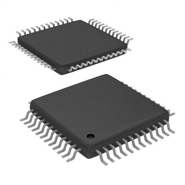
| 供应商器件封装 | 44-TQFP(10x10) |
| 包装 | 托盘 |
| 可编程输入/输出端数量 | 32 |
| 商标 | Maxim Integrated |
| 处理器系列 | DS80C323 |
| 外设 | 电源故障复位,WDT |
| 安装风格 | SMD/SMT |
| 定时器数量 | 3 Timer |
| 封装 | Tube |
| 封装/外壳 | 44-TQFP |
| 封装/箱体 | TQFP-44 |
| 工作温度 | -40°C ~ 85°C |
| 工作电源电压 | 2.7 V to 5.5 V |
| 工厂包装数量 | 160 |
| 应用说明 | 点击此处下载产品Datasheet点击此处下载产品Datasheet点击此处下载产品Datasheet点击此处下载产品Datasheet点击此处下载产品Datasheet点击此处下载产品Datasheet点击此处下载产品Datasheet点击此处下载产品Datasheet点击此处下载产品Datasheet点击此处下载产品Datasheet点击此处下载产品Datasheet |
| 振荡器类型 | 外部 |
| 接口类型 | UART |
| 数据RAM大小 | 64 kB |
| 数据Ram类型 | SRAM |
| 数据ROM大小 | 64 kB |
| 数据Rom类型 | ROM |
| 数据总线宽度 | 8 bit |
| 数据转换器 | - |
| 最大工作温度 | + 85 C |
| 最大时钟频率 | 18 MHz |
| 最小工作温度 | - 40 C |
| 标准包装 | 1 |
| 核心 | 8051 |
| 核心处理器 | 8051 |
| 核心尺寸 | 8-位 |
| 片上ADC | No |
| 电压-电源(Vcc/Vdd) | 2.7 V ~ 5.5 V |
| 电源电压-最大 | 5.5 V |
| 电源电压-最小 | 2.7 V |
| 程序存储器大小 | 64 kB |
| 程序存储器类型 | ROM |
| 程序存储容量 | - |
| 系列 | DS80C323 |
| 输入/输出端数量 | 32 I/O |
| 连接性 | EBI/EMI,SIO,UART/USART |
| 速度 | 18MHz |
| 零件号别名 | 90-80323+END DS80C323 |


- 商务部:美国ITC正式对集成电路等产品启动337调查
- 曝三星4nm工艺存在良率问题 高通将骁龙8 Gen1或转产台积电
- 太阳诱电将投资9.5亿元在常州建新厂生产MLCC 预计2023年完工
- 英特尔发布欧洲新工厂建设计划 深化IDM 2.0 战略
- 台积电先进制程称霸业界 有大客户加持明年业绩稳了
- 达到5530亿美元!SIA预计今年全球半导体销售额将创下新高
- 英特尔拟将自动驾驶子公司Mobileye上市 估值或超500亿美元
- 三星加码芯片和SET,合并消费电子和移动部门,撤换高东真等 CEO
- 三星电子宣布重大人事变动 还合并消费电子和移动部门
- 海关总署:前11个月进口集成电路产品价值2.52万亿元 增长14.8%


PDF Datasheet 数据手册内容提取
DS80C320/DS80C323 High-Speed/Low-Power Microcontrollers www .maxim-ic.com FEATURES PIN CONFIGURATIONS 80C32-Compatible TOP VIEW 8051 Pin and Instruction Set Compatible Four 8-Bit I/O Ports Three 16-Bit Timer/Counters 256 Bytes Scratchpad RAM Addresses 64kB ROM and 64kB RAM High-Speed Architecture 4 Clocks/Machine Cycle (8032 = 12) DC to 33MHz (DS80C320) DC to 18MHz (DS80C323) Single-Cycle Instruction in 121ns Uses Less Power for Equivalent Work Dual Data Pointer Optional Variable Length MOVX to Access Fast/Slow RAM/Peripherals High-Integration Controller Includes: Power-Fail Reset Programmable Watchdog Timer Early Warning Power-Fail Interrupt Two Full-Duplex Hardware Serial Ports 13 Total Interrupt Sources with Six External Available in 40-Pin DIP, 44-Pin PLCC, and 44-Pin TQFP The High-Speed Microcontroller User’s Guide must be used in conjunction with this data sheet. Download it at: www.maxim-ic.com/microcontrollers. Data sheets contain pin descriptions, feature overviews, and electrical specifications, whereas the user’s guide contains detailed information about device features and operation. Note: Some revisions of this device may incorporate deviations from published specifications known as errata. Multiple revisions of any device may be simultaneously available through various sales channels. For information about device errata, click here: www.maxim-ic.com/errata. 1 of 38 REV: 101006
DS80C320/DS80C323 High-Speed/Low-Power Microcontrollers DETAILED DESCRIPTION The DS80C320/DS80C323 are fast 80C31/80C32-compatible microcontrollers. Wasted clock and memory cycles have been removed using a redesigned processor core. As a result, every 8051 instruction is executed between 1.5 and 3 times faster than the original for the same crystal speed. Typical applications see a speed improvement of 2.5 times using the same code and same crystal. The DS80C320 offers a maximum crystal rate of 33MHz, resulting in apparent execution speeds of 82.5MHz (approximately 2.5X). The DS80C320/DS80C323 are pin compatible with all three packages of the standard 80C32 and offer the same timer/counters, serial port, and I/O ports. In short, the devices are extremely familiar to 8051 users, but provide the speed of a 16-bit processor. The DS80C320 provides several extras in addition to greater speed. These include a second full hardware serial port, seven additional interrupts, programmable watchdog timer, power-fail interrupt and reset. The device also provides dual data pointers (DPTRs) to speed block data memory moves. It can also adjust the speed of off-chip data memory access to between two and nine machine cycles for flexibility in selecting memory and peripherals. The DS80C320 operating voltage ranges from 4.25V to 5.5V, making it ideal as a high-performance upgrade to existing 5V systems. For applications in which power consumption is critical, the DS80C323 offers the same feature set as the DS80C320, but with 2.7V to 5.5V operation. Designers must have two documents to fully use all the features of this device: this data sheet and the High-Speed Microcontroller User’s Guide, available on our website at www.maxim-ic.com/microcontrollers. Data sheets contain pin descriptions, feature overviews, and electrical specifications, whereas our user’s guides contain detailed information about device features and operation. ORDERING INFORMATION Pb-FREE/RoHS- MAX CLOCK PART TEMP RANGE PIN-PACKAGE COMPLIANT SPEED (MHz) DS80C320-MCG DS80C320-MCG+ 0°C to +70°C 25 40 Plastic DIP DS80C320-QCG DS80C320-QCG+ 0°C to +70°C 25 44 PLCC DS80C320-ECG DS80C320-ECG+ 0°C to +70°C 25 44 TQFP DS80C320-MNG DS80C320-MNG+ -40°C to +85°C 25 40 Plastic DIP DS80C320-QNG DS80C320-QNG+ -40°C to +85°C 25 44 PLCC DS80C320-ENG DS80C320-ENG+ -40°C to +85°C 25 44 TQFP DS80C320-MCL DS80C320-MCL+ 0°C to +70°C 33 40 Plastic DIP DS80C320-QCL DS80C320-QCL+ 0°C to +70°C 33 44 PLCC DS80C320-ECL DS80C320-ECL+ 0°C to +70°C 33 44 TQFP DS80C320-MNL DS80C320-MNL+ -40°C to +85°C 33 40 Plastic DIP DS80C320-QNL DS80C320-QNL+ -40°C to +85°C 33 44 PLCC DS80C320-ENL DS80C320-ENL+ -40°C to +85°C 33 44 TQFP DS80C323-MCD DS80C323-MCD+ 0°C to +70°C 18 40 Plastic DIP DS80C323-QCD DS80C323-QCD+ 0°C to +70°C 18 44 PLCC DS80C323-ECD DS80C323-ECD+ 0°C to +70°C 18 44 TQFP DS80C323-QND DS80C323-QND+ -40°C to +85°C 18 44 PLCC DS80C323-END DS80C323-END+ -40°C to +85°C 18 44 TQFP + Denotes a lead(Pb)-free/RoHS-compliant device. 2 of 38
DS80C320/DS80C323 High-Speed/Low-Power Microcontrollers Figure 1. Block Diagram DS80C320/ DS80C323 PIN DESCRIPTION PIN NAME FUNCTION DIP PLCC TQFP 40 44 38 V +5V (+3V for DS80C323) CC 20 22, 23 16, 17 GND Digital Circuit Ground Reset Input. The RST input pin contains a Schmitt voltage input to recognize external active-high reset inputs. The pin also employs an 9 10 4 RST internal pulldown resistor to allow for a combination of wired OR external reset sources. An RC is not required for power-up, as the device provides this function internally. Crystal Oscillator Pins. XTAL1 and XTAL2 provide support for 18 20 14 XTAL2 parallel-resonant, AT-cut crystals. XTAL1 acts also as an input in the event that an external clock source is used in place of a crystal. XTAL2 19 21 15 XTAL1 serves as the output of the crystal amplifier. Program Store-Enable Output, Active Low. This signal is commonly connected to external ROM memory as a chip enable. PSEN provides an 29 32 26 PSEN active-low pulse width of 2.25 XTAL1 cycles with a period of four XTAL1 cycles. PSEN is driven high when data memory (RAM) is being accessed through the bus and during a reset condition. 3 of 38
DS80C320/DS80C323 High-Speed/Low-Power Microcontrollers PIN DESCRIPTION (continued) PIN NAME FUNCTION DIP PLCC TQFP Address Latch-Enable Output. This pin functions as a clock to latch the external address LSB from the multiplexed address/data bus. This signal is commonly connected to the latch enable of an external 373 30 33 27 ALE family transparent latch. ALE has a pulse width of 1.5 XTAL1 cycles and a period of four XTAL1 cycles. ALE is forced high when the device is in a reset condition. 39 43 37 AD0 Port 0, Input/Output. Port 0 is the multiplexed address/data bus. 38 42 36 AD1 During the time when ALE is high, the LSB of a memory address is 37 41 35 AD2 presented. When ALE falls, the port transitions to a bidirectional data 36 40 34 AD3 bus. This bus is used to read external ROM and read/write external 35 39 33 AD4 RAM memory or peripherals. The Port 0 has no true port latch and 34 38 32 AD5 cannot be written directly by software. The reset condition of Port 0 is 33 37 31 AD6 high. No pullup resistors are needed. 32 36 30 AD7 Port 1, I/O. Port 1 functions as both an 8-bit, bidirectional I/O port and an alternate functional interface for Timer 2 I/O, new External Interrupts, and new Serial Port 1. The reset condition of Port 1 is with all bits at logic 1. In this state, a weak pullup holds the port high. This condition also serves as an input mode, since any external circuit that writes to the port will overcome the weak pullup. When software writes a 0 to any port pin, the device will activate a strong pulldown that remains on until either a 1 is written or a reset occurs. Writing a 1 after the port has been at 0 will cause a strong transition driver to turn on, followed by a weaker sustaining pullup. Once the momentary strong driver turns off, the port once again becomes the output high (and input) state. The alternate modes of Port 1 are outlined as follows: PIN 40–44, PORT ALTERNATE FUNCTION 1–8 2–9 P1.0–P1.7 DIP PLCC TQFP 1–3 External I/O for 1 2 40 P1.0 T2 Timer/Counter 2 Timer/Counter 2 2 3 41 P1.1 T2EX Capture/Reload Trigger 3 4 42 P1.2 RXD1 Serial Port 1 Input 4 5 43 P1.3 TXD1 Serial Port 1 Output External Interrupt 2 5 6 44 P1.4 INT2 (Positive-Edge Detect) External Interrupt 3 6 7 1 P1.5 INT3 (Negative-Edge Detect) External Interrupt 4 7 8 2 P1.6 INT4 (Positive-Edge Detect) External Interrupt 5 8 9 3 P1.7 INT5 (Negative-Edge Detect) 4 of 38
DS80C320/DS80C323 High-Speed/Low-Power Microcontrollers PIN DESCRIPTION (continued) PIN NAME FUNCTION DIP PLCC TQFP 21 24 18 A8 (P2.0) Port 2, Output. Port 2 serves as the MSB for external addressing. 22 25 19 A9 (P2.1) P2.7 is A15 and P2.0 is A8. The device will automatically place the 23 26 20 A10 (P2.2) MSB of an address on P2 for external ROM and RAM access. 24 27 21 A11 (P2.3) Although Port 2 can be accessed like an ordinary I/O port, the value 25 28 22 A12 (P2.4) stored on the Port 2 latch will never be seen on the pins (due to 26 29 23 A13 (P2.5) memory access). Therefore, writing to Port 2 in software is only 27 30 24 A14 (P2.6) useful for the instructions MOVX A, @Ri or MOVX @Ri, A. These instructions use the Port 2 internal latch to supply the external address 28 31 25 A15 (P2.7) MSB. In this case, the Port 2 latch value will be supplied as the address information. Port 3, Input/Output. Port 3 functions as both an 8-bit, bidirectional I/O port and an alternate functional interface for External Interrupts, Serial Port 0, Timer 0 & 1 Inputs, RD and WR strobes. The reset condition of Port 3 is with all bits at logic 1. In this state, a weak pullup holds the port high. This condition also serves as an input mode, since any external circuit that writes to the port will overcome the weak pullup. When software writes a 0 to any port pin, the device will activate a strong pulldown that remains on until either a 1 is written or a reset occurs. Writing a 1 after the port has been at 0 will cause a strong transition driver to turn on, followed by a weaker sustaining pullup. Once the momentary strong driver turns off, the port once again becomes both the output high and input state. The alternate modes of Port 3 are outlined below: PIN PORT ALTERNATE MODE 11, 13– DIP PLCC TQFP 10–17 5, 7–13 P3.0–P3.7 19 10 11 5 P3.0 RXD0 Serial Port 0 Input 11 13 7 P3.1 TXD0 Serial Port 0 Output 12 14 8 P3.2 INT0 External Interrupt 0 13 15 9 P3.3 INT1 External Interrupt 1 14 16 10 P3.4 T0 Timer 0 External Input 15 17 11 P3.5 T1 Timer 1 External Input External Data Memory Write 16 18 12 P3.6 WR Strobe External Data Memory Read 17 19 13 P3.7 RD Strobe External Access, Active-Low Input. This pin must be connected to 31 35 29 EA ground for proper operation. No Connection (Reserved). These pins should not be connected. 12, 34, 6, 28, — N.C. They are reserved for use with future devices in this family. 1* 39* *These pins are reserved for additional ground pins on future products. 5 of 38
DS80C320/DS80C323 High-Speed/Low-Power Microcontrollers 80C32 COMPATIBILITY The DS80C320/DS80C323 are CMOS 80C32-compatible microcontrollers designed for high performance. In most cases, the devices will drop into an existing 80C32 design to significantly improve the operation. Every effort has been made to keep the devices familiar to 8032 users, yet they have many new features. In general, software written for existing 80C32-based systems will work on the DS80C320 and DS80C323. The exception is critical timing, because the high-speed microcontroller performs its instructions much faster than the original. It may be necessary to use memories with faster access times if the same crystal frequency is used. Application Note 57: DS80C320 Memory Interface Timing is a useful tool to help the embedded system designer select the proper memories for her or his application. The DS80C320/DS80C323 run the standard 8051 instruction set and is pin compatible with an 80C32 in any of three standard packages. They also provide the same timer/counter resources, full-duplex serial port, 256 bytes of scratchpad RAM, and I/O ports as the standard 80C32. Timers will default to a 12 clock-per-cycle operation to keep timing compatible with original 8051 systems. However, they can be programmed to run at the new 4 clocks per cycle if desired. New hardware features are accessed using special-function registers that do not overlap with standard 80C32 locations. A summary of these SFRs is provided below. The DS80C320/DS80C323 address memory in an identical fashion to the standard 80C32. Electrical timing appears different due to the high-speed nature of the product. However, the signals are essentially the same. Detailed timing diagrams are provided in the Electrical Specifications section. This data sheet assumes the user is familiar with the basic features of the standard 80C32. In addition to these standard features, the DS80C320/DS80C323 include many new functions. This data sheet provides only a summary and overview. Detailed descriptions are available in the High-Speed Microcontroller User’s Guide. 6 of 38
DS80C320/DS80C323 High-Speed/Low-Power Microcontrollers Figure 2. Comparative Timing of the DS80C320/DS80C323 and 80C32 DS80C320/DS80C323 TIMING STANDARD 80C32 TIMING HIGH-SPEED OPERATION The DS80C320/DS80C323 are built around a high-speed, 80C32-compatible core. Higher speed comes not just from increasing the clock frequency but also from a newer, more efficient design. In this updated core, dummy memory cycles have been eliminated. In a conventional 80C32, machine cycles are generated by dividing the clock frequency by 12. In the DS80C320/DS80C323, the same machine cycle is performed in 4 clocks. Thus the fastest instruction, one machine cycle, is executed three times faster for the same crystal frequency. Note that these are identical instructions. Figure 2 shows a comparison of the timing differences. The majority of instructions will see the full 3-to-1 speed improvement. Some instructions will get between 1.5X and 2.4X improvement. Note that all instructions are faster than the original 80C51. Table 1 shows a summary of the instruction set, including the speed. The numerical average of all op codes is approximately a 2.5-to-1 speed improvement. Individual programs are affected differently, depending on the actual instructions used. Speed-sensitive applications would make the most use of instructions that are three times faster. However, the sheer number of 3-to-1 improved op codes makes dramatic speed improvements likely for any code. The Dual Data Pointer feature also allows the user to eliminate wasted instructions when moving blocks of memory. 7 of 38
DS80C320/DS80C323 High-Speed/Low-Power Microcontrollers INSTRUCTION SET SUMMARY All instructions in the DS80C320/DS80C323 perform the same functions as their 80C32 counterparts. Their effect on bits, flags, and other status functions is identical. However, the timing of each instruction is different. This applies both in absolute and relative number of clocks. For absolute timing of real-time events, the timing of software loops will need to be calculated using the Table 1. However, counter/timers default to run at the older 12 clocks per increment. Therefore, while software runs at higher speed, timer-based events need no modification to operate as before. Timers can be set to run at 4 clocks per increment cycle to take advantage of higher speed operation. The relative time of two instructions might be different in the new architecture than it was previously. For example, in the original architecture, the “MOVX A, @DPTR” instruction and the “MOV direct, direct” instruction used two machine cycles or 24 oscillator cycles. Therefore, they required the same amount of time. In the DS80C320/DS80C323, the MOVX instruction can be done in two machine cycles or eight oscillator cycles, but the “MOV direct, direct” uses three machine cycles or 12 oscillator cycles. While both are faster than their original counterparts, they now have different execution times from each other. This is because in most cases, the DS80C320/DS80C323 use one cycle for each byte. The user concerned with precise program timing should examine the timing of each instruction for familiarity with the changes. Note that a machine cycle now requires just four clocks, and provides one ALE pulse per cycle. Many instructions require only one cycle, but some require five. In the original architecture, all were one or two cycles except for MUL and DIV. 8 of 38
DS80C320/DS80C323 High-Speed/Low-Power Microcontrollers Table 1. Instruction Set Summary SYMBOL FUNCTION SYMBOL FUNCTION A Accumulator bit direct bit-address Rn Register R7 to R0 #data 8-bit constant direct Internal Register Address #data 16 16-bit constant Internal Register pointed to by R0 or addr 16 16-bit destination address @Ri R1 (except MOVX) addr 11 11-bit destination address rel Two’s Complement Offset Byte OSCILLATOR OSCILLATOR INSTRUCTION BYTE INSTRUCTION BYTE CYCLES CYCLES ARITHMATIC INSTRUCTIONS ADD A, Rn 1 4 INC A 1 4 ADD A, direct 2 8 INC Rn 1 4 ADD A, @Ri 1 4 INC direct 2 8 ADD A, #data 2 8 INC @Ri 1 4 ADDC A, Rn 1 4 INC DPTR 1 12 ADDC A, direct 2 8 DEC A 1 4 ADDC A, @Ri 1 4 DEC Rn 1 4 ADDC A, #data 2 8 DEC direct 2 8 SUBB A, Rn 1 4 DEC @Ri 1 4 SUBB A, direct 2 8 MUL AB 1 20 SUBB A, @Ri 1 4 DIV AB 1 20 SUBB A, #data 2 8 DA A 1 4 LOGICAL INSTRUCTIONS ANL A, Rn 1 4 XRL A, Rn 1 4 ANL A, direct 2 8 XRL A, direct 2 8 ANL A, @Ri 1 4 XRL A, @Ri 1 4 ANL A, #data 2 8 XRL A, #data 2 8 ANL direct, A 2 8 XRL direct, A 2 8 ANL direct, #data 3 12 XRL direct, #data 3 12 ORL A, Rn 1 4 CLR A 1 4 ORL A, direct 2 8 CPL A 1 4 ORL A, @Ri 1 4 RL A 1 4 ORL A, #data 2 8 RLC A 1 4 ORL direct, A 2 8 RR A 1 4 ORL direct, #data 3 12 RRC A 1 4 9 of 38
DS80C320/DS80C323 High-Speed/Low-Power Microcontrollers Table 1. Instruction Set Summary (continued) OSCILLATOR OSCILLATOR INSTRUCTION BYTE INSTRUCTION BYTE CYCLES CYCLES DATA TRANSFER INSTRUCTIONS MOVC A, MOV A, Rn 1 4 1 12 @A+DPTR MOV A, direct 2 8 MOVC A, @A+PC 1 12 MOV A, @Ri 1 4 MOVX A, @Ri 1 8–36* MOV A, #data 2 8 MOVX A, @DPTR 1 8–36* MOV Rn, A 1 4 MOVX @Ri, A 1 8–36* MOV Rn, direct 2 8 MOVX @DPTR, A 1 8–36* MOV Rn, #data 2 8 PUSH direct 2 8 MOV direct, A 2 8 POP direct 2 8 MOV direct, Rn 2 8 XCH A, Rn 1 4 MOV direct1, direct2 3 12 XCH A, direct 2 8 MOV direct, @Ri 2 8 XCH A, @Ri 1 4 MOV direct, #data 3 12 XCHD A, @Ri 1 4 MOV @Ri, A 1 4 MOV @Ri, direct 2 8 MOV @Ri, #data 2 8 MOV DPTR, #data 16 3 12 BIT MANIPULATION INSTRUCTIONS CLR C 1 4 ANL C, bit 2 8 CLR bit 2 8 ANL C, bit 2 8 SETB C 1 4 ORL C, bit 2 8 SETB bit 2 8 ORL C, bit 2 8 CPL C 1 4 MOV C, bit 2 8 CPL bit 2 8 MOV bit, C 2 8 PROGRAM BRANCHING INSTRUCTIONS ACALL addr 11 2 12 CJNE A, direct, rel 3 16 LCALL addr 16 3 16 CJNE A, #data, rel 3 16 RET 1 16 CJNE Rn, #data, rel 3 16 RETI 1 16 CJNE Ri, #data, rel 3 16 AJMP addr 11 2 12 NOP 1 4 LJMP addr 16 3 16 JC rel 2 12 SJMP rel 2 12 JNC rel 2 12 JMP @A+DPTR 1 12 JB bit, rel 3 16 JZ rel 2 12 JNB bit, rel 3 16 JNZ rel 2 12 JBC bit, rel 3 16 DJNZ Rn, rel 2 12 DJNZ direct, rel 3 16 *User selectable. 10 of 38
DS80C320/DS80C323 High-Speed/Low-Power Microcontrollers Table 1 shows the speed for each class of instruction. Note that many of the instructions have multiple op codes. There are 255 op codes for 111 instructions. Of the 255 op codes, 159 are three times faster than the original 80C32. While a system that emphasizes those instructions will see the most improvement, the large total number that receive a 3 to 1 improvement assure a dramatic speed increase for any system. The speed improvement summary is provided below. SPEED ADVANTAGE SUMMARY SPEED #OP CODES IMPROVEMENT 159 3.0 x 51 1.5 x 43 2.0 x 2 2.4 x 255 Average: 2.5 MEMORY ACCESS The DS80C320/DS80C323 do not contain on-chip ROM and 256 bytes of scratchpad RAM. Off-chip memory is accessed using the multiplexed address/data bus on P0 and the MSB address on P2. Figure 3 shows a typical memory connection. Timing diagrams are provided in the Electrical Specifications section. Program memory (ROM) is accessed at a fixed rate determined by the crystal frequency and the actual instructions. As previously mentioned, an instruction cycle requires 4 clocks. Data memory (RAM) is accessed according to a variable-speed MOVX instruction as described below. Figure 3. Typical Memory Connection 11 of 38
DS80C320/DS80C323 High-Speed/Low-Power Microcontrollers STRETCH MEMORY CYCLE The DS80C320/DS80C323 allow the application software to adjust the speed of data memory access. The microcontroller is capable of performing the MOVX in as little as two instruction cycles. However, this value can be stretched as needed so that both fast memory and slow memory or peripherals can be accessed with no glue logic. Even in high-speed systems, it may not be necessary or desirable to perform data memory access at full speed. In addition, there are a variety of memory-mapped peripherals such as LCD displays or UARTs that are not fast. The Stretch MOVX is controlled by the Clock Control Register at SFR location 8Eh as described below. This allows the user to select a stretch value between 0 and 7. A Stretch of 0 will result in a two-machine cycle MOVX. A Stretch of 7 will result in a MOVX of nine machine cycles. Software can dynamically change this value depending on the particular memory or peripheral. On reset, the Stretch value will default to 1, resulting in a three-cycle MOVX. Therefore, RAM access will not be performed at full speed. This is a convenience to existing designs that may not have fast RAM in place. When maximum speed is desired, the software should select a Stretch value of 0. When using very slow RAM or peripherals, a larger stretch value can be selected. Note that this affects data memory only and the only way to slow program memory (ROM) access is to use a slower crystal. Using a Stretch value between 1 and 7 causes the microcontroller to stretch the read/write strobe and all related timing. This results in a wider read/write strobe allowing more time for memory/peripherals to respond. The timing of the variable speed MOVX is shown in the Electrical Specifications section. Note that full speed access is not the reset default case. Table 2 shows the resulting strobe widths for each Stretch value. The memory stretch is implemented using the Clock Control special-function register at SFR location 8Eh. The stretch value is selected using bits CKCON.2–0. In the table, these bits are referred to as M2 through M0. The first stretch (default) allows the use of common 120ns or 150ns RAMs without dramatically lengthening the memory access. Table 2. Data Memory Cycle Stretch Values CKCON.2–0 STROBE WIDTH MEMORY RD or WR STROBE TIME AT 25MHz MD2 MD1 MD0 CYCLES WIDTH IN CLOCKS (ns) 0 0 0 2 2 80 0 0 1 3 (default) 4 160 0 1 0 4 8 320 0 1 1 5 12 480 1 0 0 6 16 640 1 0 1 7 20 800 1 1 0 8 24 960 1 1 1 9 28 1120 12 of 38
DS80C320/DS80C323 High-Speed/Low-Power Microcontrollers DUAL DATA POINTER Data memory block moves can be accelerated using the Dual Data Pointer (DPTR). The standard 8032 DPTR is a 16-bit value that is used to address off-chip data RAM or peripherals. In the DS80C320/DS80C323, the standard 16-bit data pointer is called DPTR0 and is located at SFR addresses 82h and 83h. These are the standard locations. The new DPTR is located at SFR 84h and 85h and is called DPTR1. The DPTR Select bit (DPS) chooses the active pointer and is located at the LSB of the SFR location 86h. No other bits in register 86h have any effect and are set to 0. The user switches between data pointers by toggling the LSB of register 86h. The increment (INC) instruction is the fastest way to accomplish this. All DPTR-related instructions use the currently selected DPTR for any activity. Therefore only one instruction is required to switch from a source to a destination address. Using the Dual-Data Pointer saves code from needing to save source and destination addresses when doing a block move. Once loaded, the software simply switches between DPTR and 1. The relevant register locations are as follows. DPL 82h Low byte original DPTR DPH 83h High byte original DPTR DPL1 84h Low byte new DPTR DPH1 85h High byte new DPTR DPS 86h DPTR Select (LSB) Sample code listed below illustrates the saving from using the dual DPTR. The example program was original code written for an 8051 and requires a total of 1869 DS80C320/DS80C323 machine cycles. This takes 299s to execute at 25MHz. The new code using the Dual DPTR requires only 1097 machine cycles taking 175.5s. The Dual DPTR saves 772 machine cycles or 123.5s for a 64-byte block move. Since each pass through the loop saves 12 machine cycles when compared to the single DPTR approach, larger blocks gain more efficiency using this feature. 64-Byte Block Move without Dual Data Pointer ; SH and SL are high and low byte source address. ; DH and DL are high and low byte of destination address. # CYCLES MOV R5, #64d ; NUMBER OF BYTES TO MOVE 2 MOV DPTR, #SHSL ; LOAD SOURCE ADDRESS 3 MOV R1, #SL ; SAVE LOW BYTE OF SOURCE 2 MOV R2, #SH ; SAVE HIGH BYTE OF SOURCE 2 MOV R3, #DL ; SAVE LOW BYTE OF DESTINATION 2 MOV R4, #DH ; SAVE HIGH BYTE OF DESTINATION 2 MOVE: ; THIS LOOP IS PERFORMED THE NUMBER OF TIMES LOADED INTO R5, IN THIS EXAMPLE 64 MOVX A, @DPTR ; READ SOURCE DATA BYTE 2 MOV R1, DPL ; SAVE NEW SOURCE POINTER 2 MOV R2, DPH ; 2 MOV DPL, R3 ; LOAD NEW DESTINATION 2 MOV DPH, R4 ; 2 MOVX @DPTR, A ; WRITE DATA TO DESTINATION 2 INC DPTR ; NEXT DESTINATION ADDRESS 3 MOV R3, DPL ; SAVE NEW DESTINATION POINTER 2 MOV R4, DPH ; 2 MOV DPL, R1 ; GET NEW SOURCE POINTER 2 MOV DPH, R2 ; 2 INC DPTR ; NEXT SOURCE ADDRESS 3 DJNZ R5, MOVE ; FINISHED WITH TABLE? 3 13 of 38
DS80C320/DS80C323 High-Speed/Low-Power Microcontrollers 64-Byte Block Move with Dual Data Pointer ; SH and SL are high and low byte source address. ; DH and DL are high and low byte of destination address. ; DPS is the data pointer select. Reset condition is DPS=0, DPTR0 is selected. # CYCLES EQU DPS, #86h ; TELL ASSEMBLER ABOUT DPS MOV R5, #64 ; NUMBER OF BYTES TO MOVE 2 MOV DPTR, #DHDL ; LOAD DESTINATION ADDRESS 3 INC DPS ; CHANGE ACTIVE DPTR 2 MOV DPTR, #SHSL ; LOAD SOURCE ADDRESS 2 MOVE: ; THIS LOOP IS PERFORMED THE NUMBER OF TIMES LOADED INTO R5, IN THIS EXAMPLE 64 MOVX A, @DPTR ; READ SOURCE DATA BYTE 2 INC DPS ; CHANGE DPTR TO DESTINATION 2 MOVX @DPTR, A ; WRITE DATA TO DESTINATION 2 INC DPTR ; NEXT DESTINATION ADDRESS 3 INC DPS ; CHANGE DATA POINTER TO SOURCE 2 INC DPTR ; NEXT SOURCE ADDRESS 3 DJNZ R5, MOVE ; FINISHED WITH TABLE? 3 PERIPHERAL OVERVIEW Peripherals in the DS80C320/DS80C323 are accessed using the SFRs. The devices provide several of the most commonly needed peripheral functions in microcomputer-based systems. These functions are new to the 80C32 family and include a second serial port, power-fail reset, power-fail interrupt, and a programmable watchdog timer. These are briefly described in the following paragraphs. More details are available in the High-Speed Microcontroller User’s Guide. SERIAL PORTS The DS80C320/DS80C323 provide a serial port (UART) that is identical to the 80C32. Many applications require serial communication with multiple devices. Therefore, a second hardware serial port is provided that is a full duplicate of the standard one. It optionally uses pins P1.2 (RXD1) and P1.3 (TXD1). This port has duplicate control functions included in new SFR locations. The second serial port operates in a comparable manner with the first. Both can operate simultaneously but can be at different baud rates. The second serial port has similar control registers (SCON1 at C0h, SBUF1 at C1h) to the original. One difference is that for timer-based baud rates, the original serial port can use Timer 1 or Timer 2 to generate baud rates. This is selected via SFR bits. The new serial port can only use Timer 1. TIMER-RATE CONTROL One important difference exists between the DS80C320/DS80C323 and 80C32 regarding timers. The original 80C32 used a 12 clock-per-cycle scheme for timers and consequently for some serial baud rates (depending on the mode). The DS80C320/DS80C323 architecture normally runs using 4 clocks per cycle. However, in the area of timers, it will default to a 12 clock-per-cycle scheme on a reset. This allows existing code with real-time dependencies such as baud rates to operate properly. If an application needs higher speed timers or serial baud rates, the timers can be set to run at the 4-clock rate. The Clock Control register (CKCON - 8Eh) determines these timer speeds. When the relevant CKCON bit is a logic 1, the device uses 4 clocks per cycle to generate timer speeds. When the control bit is set to a 0, the device uses 12 clocks for timer speeds. The reset condition is a 0. CKCON.5 selects the speed of Timer 2. CKCON.4 selects Timer 1 and CKCON.3 selects Timer 0. Note that unless a user desires very fast timing, it is unnecessary to alter these bits. Note that the timer controls are independent. 14 of 38
DS80C320/DS80C323 High-Speed/Low-Power Microcontrollers POWER-FAIL RESET The DS80C320/DS80C323 incorporate a precision bandgap voltage reference to determine when V is CC out of tolerance. While powering up, internal circuits will hold the device in a reset state until V rises CC above the V reset threshold. Once V is above this level, the oscillator will begin running. An internal RST CC reset circuit will then count 65,536 clocks to allow time for power and the oscillator to stabilize. The microcontroller will then exit the reset condition. No external components are needed to generate a power on reset. During power-down or during a severe power glitch, as V falls below V , the CC RST microcontroller will also generate its own reset. It will hold the reset condition as long as power remains below the threshold. This reset will occur automatically, needing no action from the user or from the software. See the Electrical Specifications section for the exact value of V . RST POWER-FAIL INTERRUPT The same reference that generates a precision reset threshold can also generate an optional early warning Power-fail Interrupt (PFI). When enabled by the application software, this interrupt always has the highest priority. On detecting that the V has dropped below V and that the PFI is enabled, the CC PFW processor will vector to ROM address 0033h. The PFI enable is located in the Watchdog Control SFR (WDCON to D8h). Setting WDCON.5 to logic 1 will enable the PFI. The application software can also read a flag at WDCON.4. This bit is set when a PFI condition has occurred. The flag is independent of the interrupt enable and software must manually clear it. WATCHDOG TIMER For applications that cannot afford to run out of control, the DS80C320/DS80C323 incorporate a programmable watchdog timer circuit. The watchdog timer circuit resets the microcontroller if software fails to reset the watchdog before the selected time interval has elapsed. The user selects one of four timeout values. After enabling the watchdog, software must reset the timer prior to expiration of the interval, or the CPU will be reset. Both the Watchdog Enable and the Watchdog Reset bits are protected by a “Timed Access” circuit. This prevents accidentally clearing the watchdog. Timeout values are precise since they are related to the crystal frequency as shown in Table 3. For reference, the time periods at 25MHz are also shown. The watchdog timer also provides a useful option for systems that may not require a reset. If enabled, then 512 clocks before giving a reset, the watchdog will give an interrupt. The interrupt can also serve as a convenient time-base generator, or be used to wake-up the processor from Idle mode. The watchdog function is controlled in the Clock Control (CKCON to 8Eh), Watchdog Control (WDCON to D8h), and Extended Interrupt Enable (EIE to E8h) SFRs. CKCON.7 and CKCON.6 are called WD1 and WD0, respectively, and are used to select the watchdog timeout period as shown in Table 3. Table 3. Watchdog Timeout Values INTERRUPT TIME (at RESET TIME WD1 WD0 TIMEOUT 25MHz) TIMEOUT (at 25MHz) 0 0 217 clocks 5.243ms 217 + 512 clocks 5.263ms j 0 1 220 clocks 41.94ms 220 + 512 clocks 41.96ms 1 0 223 clocks 335.54ms 223 + 512 clocks 335.56ms 1 1 226 clocks 2684.35ms 226 + 512 clocks 2684.38ms As Table 3 shows, the watchdog timer uses the crystal frequency as a time base. A user selects one of four counter values to determine the timeout. These clock counter lengths are 217 = 131,072 clocks; 220 = 1,048,576; 223 = 8,388,608 clocks; or 226 = 67,108,864 clocks. The times shown in Table 4 are with 15 of 38
DS80C320/DS80C323 High-Speed/Low-Power Microcontrollers a 25MHz crystal frequency. Note that once the counter chain has reached a conclusion, the optional interrupt is generated. Regardless of whether the user enables this interrupt, there are then 512 clocks left until a reset occurs. There are 5 control bits in special function registers that affect the Watchdog Timer and two status flags that report to the user. The Reset Watchdog Timer bit (WDCON.0) should be asserted prior to modifying the Watchdog Timer Mode Select bits (WD1, WD0) to avoid corruption of the watchdog count. WDIF (WDCON.3) is the interrupt flag that is set when there are 512 clocks remaining until a reset occurs. WTRF (WDCON.2) is the flag that is set when a Watchdog reset has occurred. This allows the application software to determine the source of a reset. Setting the EWT (WDCON.1) bit enables the Watchdog Timer. The bit is protected by timed access. Setting the RWT (WDCON.0) bit restarts the Watchdog Timer for another full interval. Application software must set this bit prior to the timeout. As mentioned previously, WD1 and 0 (CKCON .7 and 6) select the timeout. Finally, the Watchdog Interrupt is enabled using EWDI (EIE.4). INTERRUPTS The DS80C320/DS80C323 provide 13 sources of interrupt with three priority levels. The Power-fail Interrupt (PFI), if enabled, always has the highest priority. There are two remaining user-selectable priorities: high and low. If two interrupts that have the same priority occur simultaneously, the natural precedence given in Table 4 determines which is acted upon. Except for the PFI, all interrupts that are new to the 8051 family have a lower natural priority than the originals. Table 4. Interrupt Priority NATURAL NAME FUNCTION VECTOR OLD/NEW PRIORITY PFI Power-Fail Interrupt 33h j 1 New INT0 External Interrupt 0 03h 2 Old TF0 Timer 0 0Bh 3 Old INT1 External Interrupt 1 13h 4 Old TF1 Timer 1 1Bh 5 Old SCON0 TI0 or RI0 from Serial Port 0 23h 6 Old TF2 Timer 2 2Bh 7 Old SCON1 TI1 or RI1 from Serial Port 1 3Bh 8 New INT2 External Interrupt 2 43h 9 New INT3 External Interrupt 3 4Bh 10 New INT4 External Interrupt 4 53h 11 New INT5 External Interrupt 5 5Bh 12 New WDTI Watchdog Timeout Interrupt 63h 13 New 16 of 38
DS80C320/DS80C323 High-Speed/Low-Power Microcontrollers POWER MANAGEMENT The DS80C320/DS80C323 provide the standard Idle and power-down (Stop) modes that are available on the standard 80C32. However, the device has enhancements that make these modes more useful, and allow more power saving. The Idle mode is invoked by setting the LSB of the Power Control register (PCON to 87h). Idle will leave internal clocks, serial port and timer running. No memory access will be performed so power is dramatically reduced. Since clocks are running, the Idle power consumption is related to crystal frequency. It should be approximately one-half the operational power. The CPU can exit the Idle state with any interrupt or a reset. The power-down or Stop mode is invoked by setting the PCON.1 bit. Stop mode is a lower power state than Idle since it turns off all internal clocking. The I of a standard Stop mode is approximately 1 µA CC but is specified in the Electrical Specifications section. The CPU will exit Stop mode from an external interrupt or a reset condition. Note that internally generated interrupts (timer, serial port, watchdog) are not useful in Idle or Stop since they require clocking activity. IDLE MODE ENHANCEMENTS A simple enhancement to Idle mode makes it substantially more useful. The innovation involves not the Idle mode itself, but the watchdog timer. As mentioned above, the Watchdog Timer provides an optional interrupt capability. This interrupt can provide a periodic interval timer to bring the DS80C320/DS80C323 out of Idle mode. This can be useful even if the Watchdog is not normally used. By enabling the Watchdog Timer and its interrupt prior to invoking Idle, a user can periodically come out of Idle perform an operation, then return to Idle until the next operation. This will lower the overall power consumption. When using the Watchdog Interrupt to cancel the Idle state, make sure to restart the Watchdog Timer or it will cause a reset. STOP MODE ENHANCEMENTS The DS80C320/DS80C323 provide two enhancements to the Stop mode. As documented above, the device provides a bandgap reference to determine Power-fail Interrupt and Reset thresholds. The default state is that the bandgap reference is off when Stop mode is invoked. This allows the extremely low power state mentioned above. A user can optionally choose to have the bandgap enabled during Stop mode. This means that PFI and power-fail reset will be activated and are valid means for leaving Stop mode. In Stop mode with the bandgap on, I will be approximately 50A compared with 1A with the bandgap CC off. If a user does not require a Power-fail Reset or Interrupt while in Stop mode, the bandgap can remain turned off. Note that only the most power sensitive applications should turn off the bandgap, as this results in an uncontrolled power-down condition. The control of the bandgap reference is located in the Extended Interrupt Flag register (EXIF to 91h). Setting BGS (EXIF.0) to a 1 will leave the bandgap reference enabled during Stop mode. The default or reset condition is with the bit at a logic 0. This results in the bandgap being turned off during Stop mode. Note that this bit has no control of the reference during full power or Idle modes. Be aware that the DS80C320 and DS80C323 require that the reset watchdog timer bit (RWT;WDCON.0) be set 17 of 38
DS80C320/DS80C323 High-Speed/Low-Power Microcontrollers immediately preceding the setting of the Stop bit to guarantee a correct power-on delay when exiting Stop mode. The second feature allows an additional power saving option. This is the ability to start instantly when exiting Stop mode. It is accomplished using an internal ring oscillator that can be used when exiting Stop mode in response to an interrupt. The benefit of the ring oscillator is as follows. Using Stop mode turns off the crystal oscillator and all internal clocks to save power. This requires that the oscillator be restarted when exiting Stop mode. Actual start-up time is crystal dependent, but is normally at least 4ms. A common recommendation is 10ms. In an application that will wakeup, perform a short operation, then return to sleep, the crystal startup can be longer than the real transaction. However, the ring oscillator will start instantly. The user can perform a simple operation and return to sleep before the crystal has even stabilized. If the ring is used to start and the processor remains running, hardware will automatically switch to the crystal once a power-on reset interval (65,536 clocks) has expired. This value is used to guarantee stability even though power is not being cycled. If the user returns to Stop mode prior to switching of crystal, then all clocks will be turned off again. The ring oscillator runs at approximately 3MHz (1.5MHz at 3V) but will not be a precision value. No real- time precision operations (including serial communication) should be conducted during this ring period. Figure 4 shows how the operation would compare when using the ring, and when starting up normally. The default state is to come out of Stop mode without using the ring oscillator. This function is controlled using the RGSL - Ring Select bit at EXIF.1 (EXIF to 91h). When EXIF.1 is set, the ring oscillator will be used to come out of Stop mode quickly. As mentioned above, the processor will automatically switch from the ring (if enabled) to the crystal after a delay of 65,536 crystal clocks. For a 3.57MHz crystal, this is approximately 18ms. The processor sets a flag called RGMD - Ring Mode to tell software that the ring is being used. This bit at EXIF.2 will be logic 1 when the ring is in use. No serial communication or precision timing should be attempted while this bit is set, since the operating frequency is not precise. 18 of 38
DS80C320/DS80C323 High-Speed/Low-Power Microcontrollers Figure 4. Ring Oscillator Startup DIAGRAM ASSUMES THAT THE OPERATION FOLLOWING STOP REQUIRES LESS THAN 18ms COMPLETE. TIMED ACCESS PROTECTION Selected SFR bits are critical to operation, making it desirable to protect against an accidental write operation. The Timed Access procedure prevents an errant CPU from accidentally altering a bit that would cause difficulty. The Timed Access procedure requires that the write of a protected bit be preceded by the following instructions: MOV 0C7h, #0AAh MOV 0C7h, #55h By writing an AAh followed by a 55h to the Timed Access register (location C7h), the hardware opens a three-cycle window that allows software to modify one of the protected bits. If the instruction that seeks to modify the protected bit is not immediately proceeded by these instructions, the write will not take effect. The protected bits are: EXIF.0 BGS Bandgap Select WDCON.6 POR Power-on Reset flag WDCON.1 EWT Enable Watchdog WDCON.0 RWT Reset Watchdog WDCON.3 WDIF Watchdog Interrupt Flag 19 of 38
DS80C320/DS80C323 High-Speed/Low-Power Microcontrollers SPECIAL-FUNCTION REGISTERS Most special features of the DS80C320/DS80C323 or 80C32 are controlled by bits in the SFRs, allowing the devices to add many features but use the same instruction set. When writing software to use a new feature, the SFR must be defined to an assembler or compiler using an equate statement. This is the only change needed to access the new function. The DS80C320/DS80C323 duplicate the SFRs that are contained in the standard 80C32. Table 5 shows the register addresses and bit locations. Many are standard 80C32 registers. The High-Speed Microcontroller User’s Guide describes all SFRs. Table 5. Special-Function Register Locations REGISTER BIT 7 BIT 6 BIT 5 BIT 4 BIT 3 BIT 2 BIT 1 BIT 0 ADDRESS SP 81h DPL 82h DPH 83h DPL1 84h DPH1 85h DPS 0 0 0 0 0 0 0 SEL 86h PCON SMOD_0 SMOD0 — — GF1 GF0 STOP IDLE 87h TCON TF1 TR1 TF0 TR0 IE1 IT1 IE0 IT0 88h TMOD GATE C/T M1 M0 GATE C/T M1 M0 89h TL0 8Ah TL1 8Bh TH0 8Ch TH1 8Dh CKCON WD1 WD0 T2M T1M T0M MD2 MD1 MD0 8Eh P1 P1.7 P1.6 P1.5 P1.4 P1.3 P1.2 P1.1 P1.0 90h EXIF IE5 IE4 IE3 IE2 — RGMD RGSL BGS 91h SCON0 SM0/FE_0 SM1_0 SM2_0 REN_0 TB8_0 RB8_0 TI_0 RI_0 98h SBUF0 99h P2 P2.0 P2.6 P2.5 P2.4 P2.3 P2.2 P2.1 P2.0 A0h IE EA ES1 ET2 ES0 ET1 EX1 ET0 EX0 A8h SADDR0 A9h SADDR1 AAh P3 P3.7 P3.6 P3.5 P3.4 P3.3 P3.2 P3.1 P3.0 B0h IP — PS1 PT2 PS0 PT1 PX1 PT0 PX0 B8h SADEN0 B9h SADEN1 BAh SCON1 SM0/FE_0 SM1_0 SM2_0 REN_0 TB8_0 RB8_0 TI_0 RI_0 C0h SBUF1 C1h STATUS PIP HIP LIP 1 1 1 1 1 C5h TA C7h T2CON TF2 EXF2 RCLK TCLK EXEN2 TR2 C/T2 CP/RL2 C8h T2MOD — — — — — — T2OE DCEN C9h RCAP2L CAh RCAP2H CBh TL2 CCh TH2 CDh PSW CY AC F0 RS1 RS0 OV FL P D0h WDCON SMOD_1 POR EPFI PFI WDIF WTRF EWT RWT D8h ACC E0h EIE — — — EWDI EX5 EX4 EX3 EX2 E8h B F0h EIP — — — PWDI PX5 PX4 PX3 PX2 F8h 20 of 38
DS80C320/DS80C323 High-Speed/Low-Power Microcontrollers ELECTRICAL SPECIFICATIONS ABSOLUTE MAXIMUM RATINGS Voltage Range on Any Pin Relative to Ground…………………………………………-0.3V to (V + 0.5V) CC Voltage Range on V Relative to Ground……………………………………………………..-0.3V to +6.0V CC Operating Temperature Range………………………………………………………………….-40°C to +85°C Storage Temperature Range…………………………………………………………………..-55°C to +125°C Soldering Temperature…………………………………………….See IPC/JEDEC J-STD-020 Specification This is a stress rating only and functional operation of the device at these or any other conditions above those indicated in the operation sections of this specification is not implied. Exposure to absolute maximum rating conditions for extended periods of time may affect reliability. DC ELECTRICAL CHARACTERISTICS—DS80C320 (V = 4.5V to 5.5V, T = -40°C to +85°C.) CC A PARAMETER SYMBOL MIN TYP MAX UNITS NOTES Operating Supply Voltage V 4.5 5.0 5.5 V 1 CC Power-Fail Warning Voltage V 4.25 4.38 4.55 V 1 PFW Minimum Operating Voltage V 4.0 4.1 4.25 V 1, 12 RST Supply Current Active Mode at 25MHz I 30 45 mA 2 CC Supply Current Idle Mode at 25MHz I 15 25 mA 3 IDLE Supply Current Active Mode at 33MHz I 35 mA 2 CC Supply Current Idle Mode at 33MHz I 20 mA 3 IDLE Supply Current Stop Mode, I 0.01 1 µA 4 Bandgap Reference Disabled STOP Supply Current Stop Mode, I 50 80 µA 4, 10 Bandgap Reference Enabled SPBG Input Low Level V -0.3 +0.8 V 1 IL Input High Level (Except XTAL1 and RST) V 2.0 V + 0.3 V 1 IH1 CC Input High Level XTAL1 and RST V 3.5 V + 0.3 V 1 IH2 CC Output-Low Voltage Ports 1, 3 V 0.45 V 1 at I = 1.6mA OL1 OL Output-Low Voltage Ports 0, 2, ALE, PSEN V 0.45 V 1, 5 OL2 at I = 3.2mA OL Output-High Voltage Ports 1, 3, ALE, PSEN V 2.4 V 1, 6 OH1 at I = -50µA OH Output High Voltage Ports 1, 3 V 2.4 V 1, 7 at I = -1.5mA OH2 OH Output-High Voltage Ports 0, 2, ALE, PSEN V 2.4 V 1, 5 OH3 at I = -8mA OH Input Low Current Ports 1, 3 at 0.45V I -55 µA 11 IL Transition Current from 1 to 0 I -650 µA 8 Ports 1, 3 at 2V TL Input Leakage Port 0, Bus Mode I -300 +300 µA 9 L RST Pulldown Resistance R 50 170 k RST 21 of 38
DS80C320/DS80C323 High-Speed/Low-Power Microcontrollers NOTES FOR DS80C320 DC ELECTRICAL CHARACTERISTICS All parameters apply to both commercial and industrial temperature operation unless otherwise noted. Specifications to -40°C are guaranteed by design and are not production tested. 1. All voltages are referenced to ground. 2. Active current is measured with a 25MHz clock source driving XTAL1, V = RST = 5.5V, all other pins CC disconnected. 3. Idle mode current is measured with a 25MHz clock source driving XTAL1, V = 5.5V, RST at ground, all CC other pins disconnected. 4. Stop mode current measured with XTAL1 and RST grounded, V = 5.5V, all other pins disconnected. CC 5. When addressing external memory. This specification only applies to the first clock cycle following transition. 6. RST = V . This condition mimics operation of pins in I/O mode. CC 7. During a 0-to-1 transition, a one-shot drives the ports hard for two clock cycles. This measurement reflects port in transition mode. 8. Ports 1 and 3 source transition current when being pulled down externally. It reaches its maximum at approximately 2V. 9. 0.45<V <V . Not a high-impedance input. This port is a weak address holding latch because Port 0 is IN CC dedicated as an address bus on the DS80C320. Peak current occurs near the input transition point of the latch, approximately 2V. 10. Over the industrial temperature range, this specification has a maximum value of 200A. 11. This is the current required from an external circuit to hold a logic low level on an I/O pin while the corresponding port latch bit is set to 1. This is only the current required to hold the low level; transitions from 1 to 0 on an I/O pin will also have to overcome the transition current. 12. Device operating range is 4.5V to 5.5V; however, device is tested to 4.0V to ensure proper operation at minimum V . RST TYPICAL I vs. FREQUENCY CC 22 of 38
DS80C320/DS80C323 High-Speed/Low-Power Microcontrollers AC CHARACTERISTICS—DS80C320 33MHz VARIABLE CLOCK PARAMETER SYMBOL UNITS MIN MAX MIN MAX External 0 33 0 33 Oscillator Oscillator 1/t MHz Frequency External CLCL 1 33 1 33 Crystal ALE Pulse Width t 34 1.5t -11 ns LHLL CLCL Port 0 Address Valid to t 4 0.5t -11 ns ALE Low AVLL CLCL Address Hold After t 2 (Note 5) 0.25t -5 (Note 5) ns ALE Low LLAX1 CLCL Address Hold After t 6 0.5t -9 ns ALE Low for MOVX WR LLAX2 CLCL ALE Low to Valid t 49 2.5t -27 ns Instruction In LLIV CLCL ALE Low to PSEN Low tLLPL 0.5 0.25tCLCL-7 ns PSEN Pulse Width tPLPH 61 2.25tCLCL-7 ns PSEN Low to Valid t 48 2.25t -21 ns PLIV CLCL Instruction In Input Instruction Hold t 0 0 ns After PSEN PXIX Input Instruction Float t 25 t -5 ns After PSEN PXIZ CLCL Port 0 Address to Valid t 64 3t -27 ns Instruction In AVIV1 CLCL Port 2 Address to Valid t 73 3.5t -33 ns Instruction In AVIV2 CLCL PSEN Low to Address Float tPLAZ (Note 5) (Note 5) ns NOTES FOR DS80C320 AC ELECTRICAL CHARACTERISTICS All parameters apply to both commercial and industrial temperature operation unless otherwise noted. Specifications to -40°C are guaranteed by design and are not production tested. AC electrical characteristics assume 50% duty cycle for the oscillator, oscillator frequency > 16MHz, and are not 100% tested, but are guaranteed by design. 1. All signals rated over operating temperature at 33MHz. 2. All signals characterized with load capacitance of 80pF except Port 0, ALE, PSEN, RD and WR at 100pF. Note that loading should be approximately equal for valid timing. 3. Interfacing to memory devices with float times (turn off times) over 30ns may cause contention. This will not damage the parts but will cause an increase in operating current. 4. Specifications assume a 50% duty cycle for the oscillator. Port 2 timing will change with the duty cycle variations. 5. Address is held in a weak latch until over driven by external memory. 23 of 38
DS80C320/DS80C323 High-Speed/Low-Power Microcontrollers MOVX CHARACTERISTICS—DS80C320 VARIABLE CLOCK PARAMETER SYMBOL UNITS STRETCH MIN MAX 2t -11 t =0 RD Pulse Width tRLRH tCLC-L11 ns tMCS>0 MCS MCS 2t -11 t =0 WR Pulse Width tWLWH CLCL ns MCS t -11 t >0 MCS MCS 2t -25 t =0 RD Low to Valid Data In tRLDV tCLC-L25 ns tMCS>0 MCS MCS Data Hold After Read t 0 ns RHDX t -5 t =0 Data Float After Read t CLCL ns MCS RHDZ 2t -5 t >0 CLCL MCS 2.5t -27 t =0 ALE Low to Valid Data In t CLCL ns MCS LLDV 1.5t -28+t t >0 CLCL MCS MCS Port 0 Address to Valid Data 3t -27 t =0 t CLCL ns MCS In AVDV1 2t -31+t t >0 CLCL MCS MCS Port 2 Address to Valid Data 3.5t -32 t =0 CLCL MCS t ns In AVDV2 2.5t -34+t t >0 CLCL MCS MCS 0.5t -8 0.5t +6 t =0 ALE Low to RD or WR Low tLLWL CLCL CLCL ns MCS 1.5t -7 1.5t +8 t >0 CLCL CLCL MCS Port 0 Address Valid to RD or tCLCL-11 tMCS=0 t ns WR Low AVWL1 2tCLCL-10 tMCS>0 Port 2 Address Valid to RD or 1.5tCLCL-9 tMCS=0 t ns AVWL2 WR Low 2.5t -13 t >0 CLCL MCS -9 t =0 MCS Data Valid to WR Transition tQVWX t -10 ns t >0 CLCL MCS t -12 t =0 Data Hold After Write t CLCL ns MCS WHQX 2t -7 t >0 CLCL MCS RD Low to Address Float tRLAZ (Note 5) ns RD or WR High to ALE t 0 10 ns tMCS=0 WHLH High t -5 t +11 t >0 CLCL CLCL MCS Note: t is a time period related to the Stretch memory cycle selection. The following table shows the value of MCS t for each Stretch selection. MCS M2 M1 M0 MOVX CYCLES t MCS 0 0 0 2 machine cycles 0 0 0 1 3 machine cycles (default) 4 t CLCL 0 1 0 4 machine cycles 8 t CLCL 0 1 1 5 machine cycles 12 t CLCL 1 0 0 6 machine cycles 16 t CLCL 1 0 1 7 machine cycles 20 t CLCL 1 1 0 8 machine cycles 24 t CLCL 1 1 1 9 machine cycles 28 t CLCL 24 of 38
DS80C320/DS80C323 High-Speed/Low-Power Microcontrollers DC ELECTRICAL CHARACTERISTICS—DS80C323 PARAMETER SYMBOL MIN TYP MAX UNITS NOTES Operating Supply Voltage V 2.7 3.0 5.5 V 1 CC Power-Fail Warning Voltage V 2.6 2.7 2.8 V 1 PFW Minimum Operating Voltage V 2.5 2.6 2.7 V 1, 12 RST Supply Current Active Mode at 18MHz I 10 mA 2 CC Supply Current Idle Mode at 18MHz I 6 mA 3 IDLE Supply Current Stop Mode, I 0.1 µA 2 Bandgap Reference Disabled STOP Supply Current Stop Mode, I 40 µA 4, 10 Bandgap Reference Enabled SPBG Input Low Level V -0.3 +0.2 x V V 1 IL CC Input High Level V 0.7 x V V +0.3 V 1 (Except XTAL1 and RST) IH1 CC CC 0.7 x V Input High Level XTAL1 and RST V CC V +0.3 V 1 IH2 +0.25V CC Output Low Voltage Ports 1, 3 V 0.4 V 1 at I = 1.6mA OL1 OL Output Low Voltage Ports 0, 2, V 0.4 V 1, 5 PSEN/ALE at I = 3.2mA OL2 OL Output High Voltage Ports 1, 3, V V DD V 1, 6 PSEN/ALE at I = -15µA OH1 -0.4V OH Output High Voltage Ports 1, 3 V V DD V 1, 7 at I = -1.5mA OH2 -0.4V OH Output High Voltage Ports 0, 2, V V DD V 1, 5 PSEN/ALE at I = -2mA OH3 -0.4V OH Input Low Current Ports 1, 3 at 0.45V I -30 µA 11 IL Transition Current from 1 0, I -400 µA 8 Ports 1, 3 at 2V TL Input Leakage Port 0, Bus Mode I -300 +300 µA 9 L RST Pulldown Resistance R 50 170 k RST NOTES FOR DS80C323 DC ELECTRICAL CHARACTERISTICS All parameters apply to both commercial and industrial temperature operation unless otherwise noted. Specifications to -40°C are guaranteed by design and are not production tested. Device operating range is 2.7V to 5.5V. DC electrical specifications are for operation 2.7V to 3.3V. 1. All voltages are referenced to ground. 2. Active mode current is measured with an 18MHz clock source driving XTAL1, V = RST = 3.3V, all other CC pins disconnected. 3. Idle mode current is measured with an 18MHz clock source driving XTAL1, V = 3.3V, all other pins CC disconnected. 4. Stop mode current measured with XTAL1 and RST grounded, V = 3.3V, all other pins disconnected. CC 5. When addressing external memory. This specification only applies to the first clock cycle following the transition. 25 of 38
DS80C320/DS80C323 High-Speed/Low-Power Microcontrollers NOTES FOR DS80C323 DC ELECTRICAL CHARACTERISTICS (continued) All parameters apply to both commercial and industrial temperature operation unless otherwise noted. Specifications to -40°C are guaranteed by design and are not production tested. Device operating range is 2.7V to 5.5V. DC electrical specifications are for operation 2.7V to 3.3V. 6. RST = V . This condition mimics operation of pins in I/O mode. CC 7. During a 0-to-1 transition, a one-shot drives the ports hard for two clock cycles. This measurement reflects port in transition mode. 8. Ports 1, 2, and 3 source transition current when being pulled down externally. It reaches its maximum at approximately 2V. 9. V between ground and V - 0.3V. Not a high-impedance input. This port is a weak address latch because IN CC Port 0 is dedicated as an address bus on the DS80C323. Peak current occurs near the input transition point of the latch, approximately 2V. 10. Over the industrial temperature range, this specification has a maximum value of 200A. 11. This is the current from an external circuit to hold a logic low level on an I/O pin while the corresponding port latch bit is set to 1. This is only the current required to hold the low level; transitions from 1 to 0 on an I/O pin will also have to overcome the transition current. 12. Device operating range is 2.7V to 5.5V, however device is tested to 2.5V to ensure proper operation at minimum V . RST 26 of 38
DS80C320/DS80C323 High-Speed/Low-Power Microcontrollers AC ELECTRICAL CHARACTERISTICS—DS80C323 18 MHz VARIABLE CLOCK PARAMETER SYMBOL UNITS MIN MAX MIN MAX External 0 18 0 18 Oscillator Oscillator 1/t MHz Frequency External CLCL 1 18 1 18 Crystal ALE Pulse Width t 68 1.5t -15 ns LHLL CLCL Port 0 Address Valid t 16 0.5t -11 ns to ALE Low AVLL CLCL Address Hold After t 6 (Note 5) 0.25t -8 (Note 5) ns ALE Low LLAX1 CLCL Address Hold After t 14 0.5t -13 ns ALE Low for MOVX WR LLAX2 CLCL ALE Low to Valid t 93 2.5t -46 ns Instruction In LLIV CLCL ALE Low to PSEN Low tLLPL 4 0.25tCLCL-10 ns PSEN Pulse Width tPLPH 118 2.25tCLCL-7 ns PSEN Low to Valid t 87 2.25t -38 ns PLIV CLCL Instruction In Input Instruction Hold t 0 0 ns After PSEN PXIX Input Instruction Float t 51 t -5 ns After PSEN PXIZ CLCL Port 0 Address to Valid t 128 3t -39 ns Instruction In AVIV1 CLCL Port 2 Address to Valid t 139 3.5t -56 ns Instruction In AVIV2 CLCL PSEN Low to Address Float tPLAZ (Note 5) (Note 5) ns NOTES FOR DS80C323 AC ELECTRICAL CHARACTERISTICS All parameters apply to both commercial and industrial temperature operation unless otherwise noted. Specifications to -40°C are guaranteed by design and are not production tested. AC electrical characteristics assume 50% duty cycle for the oscillator, oscillator frequency > 16MHz, and are not 100% production tested, but are guaranteed by design. 1. All signals rated over operating temperature at 18MHz. 2. All signals characterized with load capacitance of 80pF except Port 0, ALE, PSEN, RD, and WR at 100pF. Note that loading should be approximately equal for valid timing. 3. Interfacing to memory devices with float times (turn off times) over 35ns may cause contention. This will not damage the parts, but will cause an increase in operating current. 4. Specifications assume a 50% duty cycle for the oscillator. Port 2 timing will change with the duty cycle variations. 5. Address is held in a weak latch until over-driven by external memory. 27 of 38
DS80C320/DS80C323 High-Speed/Low-Power Microcontrollers MOVX CHARACTERISTICS—DS80C323 VARIABLE CLOCK PARAMETER SYMBOL UNITS STRETCH MIN MAX 2t -11 t =0 RD Pulse Width tRLRH CLCL ns MCS t -11 t >0 MCS MCS 2t -11 t =0 WR Pulse Width tWLWH tCLC-L11 ns tMCS>0 MCS MCS 2t -32 t =0 RD Low to Valid Data In tRLDV tCLC-L36 ns tMCS>0 MCS MCS Data Hold After Read t 0 ns RHDX t -5 t =0 Data Float After Read t CLCL ns MCS RHDZ 2t -7 t >0 CLCL MCS 2.5t -43 t =0 ALE Low to Valid Data In t CLCL ns MCS LLDV 1.5t -45+t t >0 CLCL MCS MCS Port 0 Address to Valid Data 3t -40 t =0 t CLCL ns MCS In AVDV1 2t -42+t t >0 CLCL MCS MCS Port 2 Address to Valid Data 3.5t -58 t =0 t CLCL ns MCS In AVDV2 2.5t -59+t t >0 CLCL MCS MCS 0.5t -18 0.5t +7 t =0 ALE Low to RD or WR CLCL CLCL MCS t ns Low LLWL 1.5t -11 1.5t +8 t >0 CLCL CLCL MCS Port 0 Address Valid to RD tCLCL-10 tMCS=0 t ns AVWL1 or WR Low 2tCLCL-10 tMCS>0 Port 2 Address Valid to RD 1.5tCLCL-27 tMCS=0 t ns or WR Low AVWL2 2.5tCLCL-25 tMCS>0 -14 t =0 MCS Data Valid to WR Transition tQVWX t -13 ns t >0 CLCL MCS t -15 t =0 Data Hold After Write t CLCL ns MCS WHQX 2t -13 t >0 CLCL MCS RD Low to Address Float tRLAZ (Note 5) ns -1 14 t =0 RD or WR High to MCS t ns ALE High WHLH t -5 t +16 t >0 CLCL CLCL MCS Note: t is a time period related to the Stretch memory cycle selection. The following table shows the value of MCS t for each Stretch selection. MCS M2 M1 M0 MOVX CYCLES t MCS 0 0 0 2 machine cycles 0 0 0 1 3 machine cycles (default) 4 t CLCL 0 1 0 4 machine cycles 8 t CLCL 0 1 1 5 machine cycles 12 t CLCL 1 0 0 6 machine cycles 16 t CLCL 1 0 1 7 machine cycles 20 t CLCL 1 1 0 8 machine cycles 24 t CLCL 1 1 1 9 machine cycles 28 t CLCL 28 of 38
DS80C320/DS80C323 High-Speed/Low-Power Microcontrollers EXTERNAL CLOCK CHARACTERISTICS PARAMETER SYMBOL MIN TYP MAX UNITS Clock High Time t 10 ns CHCX Clock Low Time t 10 ns CLCX Clock Rise Time t 5 ns CLCH Clock Fall Time t 5 ns CHCL SERIAL PORT MODE 0 TIMING CHARACTERISTICS PARAMETER SYMBOL CONDITIONS MIN TYP MAX UNITS SM2 = 0; 12t Serial Port Clock 12 clocks per cycle CLCL t ns Cycle Time XLXL SM2 = 1; 4t 4 clocks per cycle CLCL SM2 = 0 10t Output Data Setup to 12 clocks per cycle CLCL t ns Clock Rising Edge QVXH SM2 = 1; 3t 4 clocks per cycle CLCL SM2 = 0 2t Output Data Hold 12 clocks per cycle CLCL t ns from Clock Rising XHQX SM2 = 1; t 4 clocks per cycle CLCL SM2 = 0; t Input Data Hold After 12 clocks per cycle CLCL t ns Clock Rising XHDX SM2 = 1; t 4 clocks per cycle CLCL SM2 = 0; 11t Clock Rising Edge to 12 clocks per cycle CLCL t ns Input Data Valid XHDV SM2 = 1 2t 4 clocks per cycle CLCL EXPLANATION OF AC SYMBOLS In an effort to remain compatible with the original 8051 family, this device specifies the same parameter as such devices, using the same symbols. For completeness, the following is an explanation of the symbols. t Time Q Output data A Address R RD signal C Clock V Valid D Input data W WR signal H Logic level high X No longer a valid logic level L Logic level low Z Tri-state I Instruction P PSEN 29 of 38
DS80C320/DS80C323 High-Speed/Low-Power Microcontrollers POWER-CYCLE TIMING CHARACTERISTICS PARAMETER SYMBOL MIN TYP MAX UNITS NOTES Crystal Startup Time t 1.8 ms 1 CSU Power-On Reset Delay t 65,536 t 2 POR CLCL NOTES FOR POWER CYCLE TIMING CHARACTERISTICS 1. Startup time for crystals varies with load capacitance and manufacturer. Time shown is for an 11.0592MHz crystal manufactured by Fox crystal. 2. Reset delay is a synchronous counter of crystal oscillations after crystal startup. Counting begins when the level on the XTAL1 input meets the V criteria. At 25MHz, this time is 2.62ms. IH2 PROGRAM MEMORY READ CYCLE 30 of 38
DS80C320/DS80C323 High-Speed/Low-Power Microcontrollers DATA MEMORY READ CYCLE 31 of 38
DS80C320/DS80C323 High-Speed/Low-Power Microcontrollers DATA MEMORY WRITE CYCLE DATA MEMORY WRITE WITH STRETCH = 1 32 of 38
DS80C320/DS80C323 High-Speed/Low-Power Microcontrollers DATA MEMORY WRITE WITH STRETCH = 2 4-CYCLE DATA MEMORY WRITE STRETCH VALUE = 2 EXTERNAL CLOCK DRIVE 33 of 38
DS80C320/DS80C323 High-Speed/Low-Power Microcontrollers SERIAL PORT MODE 0 TIMING SERIAL PORT 0 (SYNCHRONOUS MODE) HIGH SPEED OPERATION SM2 = 1 ≥ TXD CLOCK = XTAL/4 SERIAL PORT 0 (SYNCHRONOUS MODE) SM2 = 0 ≥ TXD CLOCK = XTAL/12 34 of 38
DS80C320/DS80C323 High-Speed/Low-Power Microcontrollers POWER-CYCLE TIMING 35 of 38
DS80C320/DS80C323 High-Speed/Low-Power Microcontrollers PACKAGE INFORMATION For the latest package outline information and land patterns, go to www.maxim-ic.com/packages. PACKAGE TYPE PACKAGE CODE DOCUMENT NO. 44 TQFP C44+2 21-0293 44 MQFP M44+10 21-0269 44 MQFP M44+5 21-0826 40 PDIP P40+1 21-0044 44 PLCC Q44+1 21-0049 36 of 38
DS80C320/DS80C323 High-Speed/Low-Power Microcontrollers DATA SHEET REVISION SUMMARY The following represent the key differences between the 101006 and 070505 version of the DS80C320/DS80C323 data sheet. Please review this summary carefully. 1. Deleted DS80C323-MND from Ordering Information table (page 2). Device was never manufactured. The following represent the key differences between the 070505 and 051804 version of the DS80C320/DS80C323 data sheet. Please review this summary carefully. 2. Added Pb-free/RoHS-compliant part numbers to Ordering Information table. 3. Deleted the “A” from the IPC/JEDEC J-STD-020 specification in the Absolute Maximum Ratings. The following represent the key differences between the 051804 and the 112299 version of the DS80C320/DS80C323 data sheet. Please review this summary carefully. 1. Removed “Preliminary” status as a result of final characterization. 2. Added industrial temperature DS80C323 devices to ordering information. 3. Updated soldering temperature specification to reflect JEDEC standards. 4. Updated the following DS80C323 AC timing parameters with final characterization data: t , t , t , t , LHLL LLAX1 LLAX2 LLAX2 t , t , t , t , t , t , t , t , t , t , t , t , t , t , t . LLIV LLPL PLIV AVIV1 RLDV RHDZ LLDV AVDV1 AVDV2 LLWL AVWL1 AVWL2 QVWX WHQX WHLH 5. Updated the following DS80C320 AC timing parameters with final characterization data: t , t , t , tLLDV, WHQX LHLL LLAX2 t , t , t , t . AVDV1 LLWL AVWL1 AVWL2 6. Added note advising the need to reset watchdog timer before setting the Stop bit. 7. Added note clarifying drive strength of P0, P2, ALE, PSEN. 8. Obsoleted DS80C320 25MHz AC timing tables; merged into 33MHz AC timing tables. 9. Corrected Serial Port Mode 0 Timing diagrams to show correct order of D6, D7. The following represent the key differences between the 041896 and the 052799 version of the DS80C320 data sheet. Please review this summary carefully. 1. Corrected V pin description to show DS80C323 operation at +3V. CC 2. Corrected Timed Access description to show three-cycle window. 3. Modified absolute Maximum Ratings for any pin relative to around, V relative to ground. CC 4. Changed minimum oscillator frequency to 1MHz when using external crystal. 5. Clarified that t begins when XTAL1 reaches V . POR IH2 The following represent the key differences between the 103196 and the 041896 version of the DS80C320 data sheet. Please review this summary carefully. 1. Updated DS80C320 25MHz AC Characteristics. The following represent the key differences between the 041895 and the 031096 version of the DS80C320 data sheet. Please review this summary carefully. 1. Remove Port 0, Port 2 from V specification (PCN B60802). OH1 2. V test specification clarified (RST = V ). OH1 CC 3. Add t marking to External Memory Read Cycle figure. AVWL2 4. Correct TQFP drawing to read 44-pin TQFP. 5. Rotate page 1 TQFP illustration to match assembly specifications. The following represent the key differences between the 031096 and the 052296 version of the DS80C320 data sheet. Please review this summary carefully. 1. Added Data Sheet Revision Summary section. The following represent the key differences between 05/23/96 and 05/22/96 version of the DS80C320 data sheet and between 05/23/96 and 03/27/95 version of the DS80C323 data sheet. Please review this summary carefully. DS80C320: 1. Add DS80C323 Characteristics. 2. Change DS80C320 V specification from 4.5V to 4.55V (PCN E62802). PFW 3. Update DS80C320 33MHz AC Characteristics. DS80C323: 1. Delete Data Sheet. Contents moved to DS80C320/DS80C323. 37 of 38
DS80C320/DS80C323 High-Speed/Low-Power Microcontrollers DATA SHEET REVISION SUMMARY (continued) The following represent the key differences between the 05/22/96 and the 10/21/97 version of the DS80C320 data sheet. Please review this summary carefully. DS80C320 1. Added note to clarify I specification. IL 2. Added note to clarify AC timing conditions. 3. Corrected erroneous t label on figure “Serial Port Mode 0 Timing” to read t . QVXL QVXH 4. Added note to prevent accidental corruption of Watchdog Timer count while changing counter length. DS80C323 1. Added note to clarify I specification. IL 2. Remove port 2 from V specification, add port 3. OH1 3. I for V specification changed from -3mA to -2mA. OH OH3 4. Added note to clarify AC timing conditions. 38 of 38 Maxim/Dallas Semiconductor cannot assume responsibility for use of any circuitry other than circuitry entirely embodied in a Maxim/Dallas Semiconductor product. No circuit patent licenses are implied. Maxim/Dallas Semiconductor reserves the right to change the circuitry and specifications without notice at any time. Maxim Integrated Products, 120 San Gabriel Drive, Sunnyvale, CA 94086 408-737-7600 © 2006 Maxim Integrated Products The Maxim logo is a registered trademark of Maxim Integrated Products, Inc. The Dallas logo is a registered trademark of Dallas Semiconductor Corporation.
Mouser Electronics Authorized Distributor Click to View Pricing, Inventory, Delivery & Lifecycle Information: M axim Integrated: DS80C320-ENG+ DS80C320-ENL+ DS80C320-FCG DS80C320-FCG+ DS80C320-FNG+ DS80C320-MCG DS80C320-MCL DS80C320-MNG DS80C320-MNL DS80C320-MNL+ DS80C320-QCG DS80C320-QCG+T&R DS80C320-QCL DS80C320-QCL+T&R DS80C320-QCL/T&R DS80C320-QNG DS80C320-QNG+T&R DS80C320- QNL DS80C320-QNL+T&R DS80C323-ECD+T&R DS80C323-MCD DS80C323-QCD DS80C323-QCD+ DS80C323-QCD+T&R DS80C323-QCD/T&R DS80C323-QND DS80C323-QND+ DS80C323-QND+T&R DS80C323- QND/T&R DS80C320-ECG+ DS80C320-ECL+ DS80C320-MCG+ DS80C320-MCL+ DS80C320-MNG+ DS80C320- QCG+ DS80C320-QCL+ DS80C320-QNG+ DS80C320-QNL+ DS80C323-ECD+ DS80C323-END+ DS80C323- MCD+