ICGOO在线商城 > 集成电路(IC) > 线性 - 放大器 - 仪表,运算放大器,缓冲器放大器 > MCP6V31T-E/OT

 Datasheet下载
- 型号: MCP6V31T-E/OT
- 制造商: Microchip
- 库位|库存: xxxx|xxxx
- 要求:
| 数量阶梯 | 香港交货 | 国内含税 |
| +xxxx | $xxxx | ¥xxxx |
查看当月历史价格
查看今年历史价格
MCP6V31T-E/OT产品简介:
ICGOO电子元器件商城为您提供MCP6V31T-E/OT由Microchip设计生产,在icgoo商城现货销售,并且可以通过原厂、代理商等渠道进行代购。 MCP6V31T-E/OT价格参考¥8.91-¥8.91。MicrochipMCP6V31T-E/OT封装/规格:线性 - 放大器 - 仪表,运算放大器,缓冲器放大器, 零漂移 放大器 1 电路 满摆幅 SOT-23-5。您可以下载MCP6V31T-E/OT参考资料、Datasheet数据手册功能说明书,资料中有MCP6V31T-E/OT 详细功能的应用电路图电压和使用方法及教程。
MCP6V31T-E/OT 是 Microchip Technology 公司生产的低功耗、零漂移运算放大器,属于线性 - 放大器 - 仪表、运算放大器、缓冲器放大器类别。其应用场景广泛,尤其适用于对精度和低功耗要求较高的系统设计。以下是该型号的主要应用场景:

1. 工业自动化与控制
   MCP6V31T-E/OT 的高精度和低偏移特性使其非常适合用于工业传感器信号调理。例如,在温度、压力或湿度传感器中,可以放大微弱的模拟信号并减少噪声干扰,从而提高测量精度。

2. 医疗设备
   在医疗领域,如心电图(ECG)、血压监测仪等设备中,需要处理非常微弱的生物电信号。MCP6V31T-E/OT 的零漂移特性和低噪声性能确保了这些信号能够被准确捕捉和放大。

3. 消费电子
   对于便携式设备(如可穿戴设备、智能家居控制器),低功耗是关键因素之一。MCP6V31T-E/OT 的超低功耗设计延长了电池寿命,同时提供稳定的信号放大功能。

4. 汽车电子
   在汽车应用中,如胎压监测系统(TPMS)或车载传感器网络,该放大器的鲁棒性和抗干扰能力有助于在复杂电磁环境中保持信号完整性。

5. 物联网(IoT)节点
   IoT 设备通常需要长时间运行且依赖小型电池供电。MCP6V31T-E/OT 的低功耗和高精度特性非常适合用作数据采集模块中的信号放大器。

6. 音频处理
   在低功耗音频设备中,如麦克风前置放大器或耳机驱动电路,该器件能够提供清晰的音频信号放大,同时保持低失真。

总之,MCP6V31T-E/OT 凭借其零漂移、低功耗和高精度的特点,成为众多精密信号处理场景的理想选择。
| 参数 | 数值 |
| -3db带宽 | - |
| 产品目录 | 集成电路 (IC)半导体 |
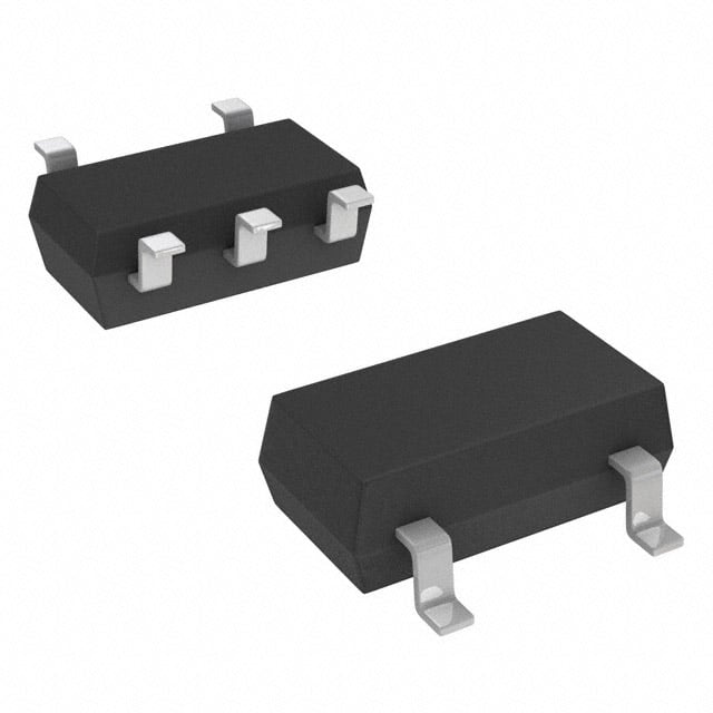
| 描述 | IC OPAMP ZRO-DRFT 300KHZ SOT23-5运算放大器 - 运放 Single, Zero Drift Op Amp, E Temp |
| 产品分类 | Linear - Amplifiers - Instrumentation, OP Amps, Buffer Amps集成电路 - IC |
| 品牌 | Microchip Technology |
| 产品手册 | |
| 产品图片 |
|
| rohs | 符合RoHS无铅 / 符合限制有害物质指令(RoHS)规范要求 |
| 产品系列 | 放大器 IC,运算放大器 - 运放,Microchip Technology MCP6V31T-E/OT- |
| 数据手册 | http://www.microchip.com/mymicrochip/filehandler.aspx?ddocname=en557758 |
| 产品型号 | MCP6V31T-E/OT |
| PCN设计/规格 | http://www.microchip.com/mymicrochip/NotificationDetails.aspx?id=5838&print=view |
| 产品种类 | 运算放大器 - 运放 |
| 供应商器件封装 | SOT-23-5 |
| 共模抑制比—最小值 | 135 dB |
| 关闭 | No Shutdown |
| 其它名称 | MCP6V31T-E/OTCT |
| 包装 | 剪切带 (CT) |
| 压摆率 | 0.13 V/µs |
| 商标 | Microchip Technology |
| 增益带宽生成 | 300 kHz |
| 增益带宽积 | 300kHz |
| 安装类型 | 表面贴装 |
| 安装风格 | SMD/SMT |
| 封装 | Reel |
| 封装/外壳 | SC-74A,SOT-753 |
| 封装/箱体 | SOT23-5 |
| 工作温度 | -40°C ~ 125°C |
| 工作电源电压 | 1.8 V to 5.5 V |
| 工厂包装数量 | 3000 |
| 放大器类型 | 零漂移 |
| 最大工作温度 | + 125 C |
| 最小工作温度 | - 40 C |
| 标准包装 | 1 |
| 电压-电源,单/双 (±) | 1.8 V ~ 5.5 V |
| 电压-输入失调 | 8µV |
| 电流-电源 | 23µA |
| 电流-输入偏置 | 5pA |
| 电流-输出/通道 | 21mA |
| 电源电流 | 23 uA |
| 电路数 | 1 |
| 系列 | MCP6V31/1U |
| 转换速度 | 0.13 V/us |
| 输入偏压电流—最大 | 5 pA |
| 输入补偿电压 | 8 uV |
| 输出电流 | 21 mA |
| 输出类型 | 满摆幅 |
| 通道数量 | 1 Channel |


- 商务部:美国ITC正式对集成电路等产品启动337调查
- 曝三星4nm工艺存在良率问题 高通将骁龙8 Gen1或转产台积电
- 太阳诱电将投资9.5亿元在常州建新厂生产MLCC 预计2023年完工
- 英特尔发布欧洲新工厂建设计划 深化IDM 2.0 战略
- 台积电先进制程称霸业界 有大客户加持明年业绩稳了
- 达到5530亿美元!SIA预计今年全球半导体销售额将创下新高
- 英特尔拟将自动驾驶子公司Mobileye上市 估值或超500亿美元
- 三星加码芯片和SET,合并消费电子和移动部门,撤换高东真等 CEO
- 三星电子宣布重大人事变动 还合并消费电子和移动部门
- 海关总署:前11个月进口集成电路产品价值2.52万亿元 增长14.8%


PDF Datasheet 数据手册内容提取
MCP6V31/1U 23 µA, 300 kHz Zero-Drift Op Amps Features Description • High DC Precision: The Microchip Technology Inc. MCP6V31/1U family of - V Drift: ±50nV/°C (maximum) operational amplifiers provides input offset voltage OS correction for very low offset and offset drift. These are - V : ±8µV (maximum) OS low power devices, with a gain bandwidth product of - A : 120dB (minimum, V =5.5V) OL DD 300kHz (typical). They are unity gain stable, have no - PSRR: 120dB (minimum, V =5.5V) DD 1/f noise, and have good Power Supply Rejection Ratio - CMRR: 120dB (minimum, VDD=5.5V) (PSRR) and Common Mode Rejection Ratio (CMRR). - E : 1.0µV (typical), f=0.1Hz to 10Hz These products operate with a single supply voltage as ni P-P - E : 0.33µV (typical), f=0.01Hz to 1Hz low as 1.8V, while drawing 23µA/amplifier (typical) of ni P-P quiescent current. • Low Power and Supply Voltages: - I : 23µA/amplifier (typical) The Microchip Technology Inc. MCP6V31/1U op amps Q are offered in single (MCP6V31 and MCP6V31U) - Wide Supply Voltage Range: 1.8V to 5.5V packages. They were designed using an advanced • Small Packages CMOS process. - Singles in SC70, SOT-23 • Easy to Use: Package Types - Rail-to-Rail Input/Output MCP6V31 MCP6V31U - Gain Bandwidth Product: 300kHz (typical) SOT-23 SC70, SOT-23 - Unity Gain Stable • Extended Temperature Range: -40°C to +125°C VOUT 1 5 VDD VIN+ 1 5 VDD VSS 2 VSS 2 Typical Applications VIN+ 3 4 VIN– VIN– 3 4 VOUT • Portable Instrumentation • Sensor Conditioning Typical Application Circuit • Temperature Measurement • DC Offset Correction R R 1 3 • Medical Instrumentation VIN VOUT R 2 C R Design Aids 2 4 U 1 • SPICE Macro Models • FilterLab® Software R2 R5 MCP6XXX V /2 U • Microchip Advanced Part Selector (MAPS) DD 2 VDD/2 MCP6V31 • Analog Demonstration and Evaluation Boards OffsetVoltageCorrectionforPowerDriver • Application Notes Related Parts • MCP6V01/2/3: Auto-Zeroed, Spread Clock • MCP6V06/7/8: Auto-Zeroed • MCP6V26/7/8: Auto-Zeroed, Low Noise • MCP6V11/1U: Zero-Drift, Low Power © 2012 Microchip Technology Inc. DS25127A-page 1
MCP6V31/1U NOTES: DS25127A-page 2 © 2012 Microchip Technology Inc.
MCP6V31/1U 1.0 ELECTRICAL CHARACTERISTICS 1.1 Absolute Maximum Ratings † V –V .................................................................................................................................................................6.5V DD SS Current at Input Pins ..............................................................................................................................................±2mA Analog Inputs (V + and V –)(Note1) .....................................................................................V –1.0V to V +1.0V IN IN SS DD All other Inputs and Outputs .......................................................................................................V –0.3V to V +0.3V SS DD Difference Input voltage .................................................................................................................................|V –V | DD SS Output Short Circuit Current ...........................................................................................................................Continuous Current at Output and Supply Pins ......................................................................................................................±30mA Storage Temperature .............................................................................................................................-65°C to +150°C Maximum Junction Temperature ..........................................................................................................................+150°C ESD protection on all pins (HBM, CDM, MM) ...........................................................................................≥2kV,1.5kV,400V Note1: See Section4.2.1, Rail-to-Rail Inputs. †Notice: Stresses above those listed under “Absolute Maximum Ratings” may cause permanent damage to the device. This is a stress rating only and functional operation of the device at those or any other conditions above those indicated in the operational listings of this specification is not implied. Exposure to maximum rating conditions for extended periods may affect device reliability. 1.2 Specifications TABLE 1-1: DC ELECTRICAL SPECIFICATIONS Electrical Characteristics: Unless otherwise indicated, T = +25°C, V = +1.8V to +5.5V, V = GND, A DD SS V = V /3,V =V /2, V =V /2, R = 100kΩ to V and C = 20pF (refer to Figure1-4 and Figure1-5). CM DD OUT DD L DD L L L Parameters Sym. Min. Typ. Max. Units Conditions Input Offset Input Offset Voltage V -8 — +8 µV T = +25°C OS A Input Offset Voltage Drift with TC -50 — +50 nV/°C T = -40 to +125°C 1 A Temperature (Linear Temp. Co.) (Note1) Input Offset Voltage Quadratic TC — ±0.08 — nV/°C2 T = -40 to +125°C 2 A Temp. Co. Power Supply Rejection PSRR 120 135 — dB Input Bias Current and Impedance Input Bias Current I — +5 — pA B Input Bias Current across Temperature I — +20 — pA T = +85°C B A I 0 +2.9 +5 nA T = +125°C B A Input Offset Current I — ±130 — pA OS Input Offset Current across Temperature I — ±140 — pA T = +85°C OS A I -1 ±0.4 +1 nA T = +125°C OS A Common Mode Input Impedance Z — 1013||6 — Ω||pF CM Differential Input Impedance Z — 1013||6 — Ω||pF DIFF Note 1: For Design Guidance only; not tested. 2: Figure2-18 shows how V and V changed across temperature for the first production lot. CML CMH © 2012 Microchip Technology Inc. DS25127A-page 3
MCP6V31/1U TABLE 1-1: DC ELECTRICAL SPECIFICATIONS (CONTINUED) Electrical Characteristics: Unless otherwise indicated, T = +25°C, V = +1.8V to +5.5V, V = GND, A DD SS V = V /3,V =V /2, V =V /2, R = 100kΩ to V and C = 20pF (refer to Figure1-4 and Figure1-5). CM DD OUT DD L DD L L L Parameters Sym. Min. Typ. Max. Units Conditions Common Mode Common-Mode V — — V −0.15 V (Note2) CML SS Input Voltage Range Low Common-Mode V V +0.2 — — V (Note2) CMH DD Input Voltage Range High Common-Mode Rejection CMRR 110 125 — dB V = 1.8V, DD V = -0.15V to 2.0V CM (Note2) CMRR 120 135 — dB V = 5.5V, DD V = -0.15V to 5.7V CM (Note2) Open-Loop Gain DC Open-Loop Gain (large signal) A 103 125 — dB V =1.8V, OL DD V = 0.3V to 1.6V OUT A 120 135 — dB V =5.5V, OL DD V = 0.3V to 5.3V OUT Output Minimum Output Voltage Swing V V V +14 V +45 mV R =10kΩ, G = +2, OL SS SS SS L 0.5V input overdrive V — V +1.4 — mV R =100kΩ, G = +2, OL SS L 0.5V input overdrive Maximum Output Voltage Swing V V –45 V –14 V mV R =10kΩ, G = +2, OH DD DD DD L 0.5V input overdrive V — V –1.4 — mV R =100kΩ, G = +2, OH DD L 0.5V input overdrive Output Short Circuit Current I — ±6 — mA V =1.8V SC DD I — ±21 — mA V =5.5V SC DD Power Supply Supply Voltage V 1.8 — 5.5 V DD Quiescent Current per amplifier I 12 23 34 µA I = 0 Q O POR Trip Voltage V 0.9 — 1.6 V POR Note 1: For Design Guidance only; not tested. 2: Figure2-18 shows how V and V changed across temperature for the first production lot. CML CMH DS25127A-page 4 © 2012 Microchip Technology Inc.
MCP6V31/1U TABLE 1-2: AC ELECTRICAL SPECIFICATIONS Electrical Characteristics: Unless otherwise indicated, T = +25°C, V = +1.8V to +5.5V, V = GND, A DD SS V = V /3, V =V /2, V =V /2, R =100kΩ to V and C =20pF (refer to Figure1-4 and Figure1-5). CM DD OUT DD L DD L L L Parameters Sym. Min. Typ. Max. Units Conditions Amplifier AC Response Gain Bandwidth Product GBWP — 300 — kHz Slew Rate SR — 0.13 — V/µs Phase Margin PM — 70 — ° G = +1 Amplifier Noise Response Input Noise Voltage E — 0.33 — µV f = 0.01Hz to 1Hz ni P-P E — 1.0 — µV f = 0.1Hz to 10Hz ni P-P Input Noise Voltage Density e — 50 — nV/√Hz f < 2kHz ni Input Noise Current Density i — 5 — fA/√Hz ni Amplifier Distortion (Note1) Intermodulation Distortion (AC) IMD — 52 — µV V tone = 50mV at 100Hz, G = 1 PK CM PK N Amplifier Step Response Start Up Time t — 2 — ms G=+1, 0.1% V settling (Note2) STR OUT Offset Correction Settling Time t — 100 — µs G = +1, V step of 2V, STL IN V within 100µV of its final value OS Output Overdrive Recovery Time t — 120 — µs G = -10, ±0.5V input overdrive to V /2, ODR DD V 50% point to V 90% point (Note3) IN OUT Note 1: These parameters were characterized using the circuit in Figure1-6. In Figure2-36 and Figure2-37, there is an IMD tone at DC, a residual tone at 100Hz and other IMD tones and clock tones. 2: High gains behave differently; see Section4.3.3, Offset at Power Up. 3: t includes some uncertainty due to clock edge timing. ODR TABLE 1-3: TEMPERATURE SPECIFICATIONS Electrical Characteristics: Unless otherwise indicated, all limits are specified for: V = +1.8V to +5.5V, DD V = GND. SS Parameters Sym. Min. Typ. Max. Units Conditions Temperature Ranges Specified Temperature Range T -40 — +125 °C A Operating Temperature Range T -40 — +125 °C (Note1) A Storage Temperature Range T -65 — +150 °C A Thermal Package Resistances Thermal Resistance, 5L-SC-70 θ — 331 — °C/W JA Thermal Resistance, 5L-SOT-23 θ — 256 — °C/W JA Note 1: Operation must not cause T to exceed Maximum Junction Temperature specification (+150°C). J © 2012 Microchip Technology Inc. DS25127A-page 5
MCP6V31/1U 1.3 Timing Diagrams 1.4 Test Circuits The circuits used for most DC and AC tests are shown 1.8Vto5.5V in Figure1-4 and Figure1-5. Lay the bypass capacitors 1.8V V 0V out as discussed in Section4.3.10, Supply Bypassing DD and Filtering. R is equal to the parallel combination of N tSTR 1.001(VDD/3) RF and RG to minimize bias current effects. VOUT 0.999(VDD/3) VDD 1µF FIGURE 1-1: Amplifier Start Up. VIN RN RISO VOUT MCP6V3X VIN 100nF CL RL V /3 t DD STL V +100µV OS V R R L V G F OS VOS–100µV FIGURE 1-4: AC and DC Test Circuit for Most Non-Inverting Gain Conditions. FIGURE 1-2: Offset Correction Settling Time. V DD 1µF VIN VDD/3 RN RISO VOUT MCP6V3X t ODR C R 100nF L L V V IN DD V t R R L ODR G F V OUT V /2 FIGURE 1-5: AC and DC Test Circuit for DD Most Inverting Gain Conditions. V SS The circuit in Figure1-6 tests the input’s dynamic FIGURE 1-3: Output Overdrive Recovery. behavior (i.e., IMD, t , t and t ). The STR STL ODR potentiometer balances the resistor network (V OUT should equal V at DC). The op amp’s common REF mode input voltage is V =V /2. The error at the CM IN input (V ) appears at V with a noise gain of ERR OUT 10V/V. 11.0kΩ 100kΩ 500Ω 0.1% 0.1% 25turn V =V /3 REF DD V DD R ISO 1µF 0Ω V OUT V IN 100nF C R L L MCP6V3X 20pF open V L 11.0kΩ 100kΩ 249Ω 0.1% 0.1% 1% FIGURE 1-6: Test Circuit for Dynamic Input Behavior. DS25127A-page 6 © 2012 Microchip Technology Inc.
MCP6V31/1U 2.0 TYPICAL PERFORMANCE CURVES Note: The graphs and tables provided following this note are a statistical summary based on a limited number of samples and are provided for informational purposes only. The performance characteristics listed herein are not tested or guaranteed. In some graphs or tables, the data presented may be outside the specified operating range (e.g., outside specified power supply range) and therefore outside the warranted range. Note: Unless otherwise indicated, T =+25°C, V =+1.8V to 5.5V, V =GND, V =V /3, V =V /2, A DD SS CM DD OUT DD V =V /2, R =100kΩ to V and C = 20pF. L DD L L L 2.1 DC Input Precision 25% 8 s 4T2A =Sa+m25p°lCes 66 VRRCeeMpprr=ee ssVeeCnnMLttaattiivveePPaarrtt ce20% VDD= 1.8V and 5.5V V) Occurren15% e (μoltage42 age of ent10% VOffsetVutO--0024 ++++188225555°°°CCCC Perc 5% Inp-6 -40°C 0% -8 -8 -7 -6 -5 -4 -3 -2 -1 0 1 2 3 4 5 6 7 8 0.0 0.5 1.0 1.5 2.0 2.5 3.0 3.5 4.0 4.5 5.0 5.5 6.0 6.5 Input Offset Voltage (μV) Power Supply Voltage (V) FIGURE 2-1: Input Offset Voltage. FIGURE 2-4: Input Offset Voltage vs. Power Supply Voltage with V =V . CM CML 35% 8 42 Samples VCM= VCMH ces30% VDD= 1.8V and 5.5V V)66 Reppresentative Part Occurren2205%% e (μoltage42 age of 15% VOffsetVO-002 ++1882555°°CCC cent10% put-4 +-2450°°CC Per 5% In-6 0% -8 -50 -40 -30 -20 -10 0 10 20 30 40 50 0.0 0.5 1.0 1.5 2.0 2.5 3.0 3.5 4.0 4.5 5.0 5.5 6.0 6.5 Input Offset Voltage Drift; TC (nV/°C) Power Supply Voltage (V) 1 FIGURE 2-2: Input Offset Voltage Drift. FIGURE 2-5: Input Offset Voltage vs. Power Supply Voltage with V =V . CM CMH 45% 8 42 Samples Representative Part es40% VDD= 1.8V and 5.5V 66 nc35% V) urre30% e (μe 4 e of Occ2205%% VoltagetV 020 VDD= 1.8V ntagn15% OffsO-2 VDD= 5.5V ce10% ut-4 Per 5% InpI-6 0% -0.5 -0.4 -0.3 -0.2 -0.1 0.0 0.1 0.2 0.3 0.4 0.5 -88 Input Offset Voltage's Quadratic Temp Co; 0.0 0.5 1.0 1.5 2.0 2.5 3.0 3.5 4.0 4.5 5.0 5.5 TC (nV/°C2) Power Supply Voltage (V) 2 FIGURE 2-3: Input Offset Voltage FIGURE 2-6: Input Offset Voltage vs. Quadratic Temp. Co. Output Voltage. © 2012 Microchip Technology Inc. DS25127A-page 7
MCP6V31/1U Note: Unless otherwise indicated, T =+25°C, V =+1.8V to 5.5V, V =GND, V =V /3, V =V /2, A DD SS CM DD OUT DD V =V /2, R =100kΩ to V and C = 20pF. L DD L L L 8 50% 66 VRRDeeDpprr=ee 1ss.ee8nnVttaattiivveePPaarrtt ss45% 2T0A =S a+m25p°lCes V) ce40% e (μoltage 42 rrenOccur333505%%% VOffsetVO-002 age of a222505%%% ut-4 +125°C ent15% Inp-6 +++-42280555°°°CCCC ercPe105%% -8 0% -0.5 0.0 0.5 1.0 1.5 2.0 2.5 -1.0 -0.8 -0.6 -0.4 -0.2 0.0 0.2 0.4 0.6 0.8 1.0 Input Common Mode Voltage (V) 1/PSRR (μV/V) FIGURE 2-7: Input Offset Voltage vs. FIGURE 2-10: PSRR. Common Mode Voltage with V =1.8V. DD 8 90% 66 VRRDeeDpprr=ee 5ss.ee5nnVttaattiivveePPaarrtt ss80% 2T1A =S a+m25p°lCes e (μV)oltage 42 rrenceOccur67560000%%%% VDD= 5.5V VsetV 00 e of 40% OffO-2 aga3300%% put-4 ++18255°C°C cent20% In-6 ++-422055°°CCC erPe10% VVDDDD=11..88VV -8 0% 0.5 0.0 0.5 1.0 1.5 2.0 2.5 3.0 3.5 4.0 4.5 5.0 5.5 6.0 -0.5 -0.4 -0.3 -0.2 -0.1 0.0 0.1 0.2 0.3 0.4 0.5 - Input Common Mode Voltage (V) 1/A (μV/V) OL FIGURE 2-8: Input Offset Voltage vs. FIGURE 2-11: DC Open-Loop Gain. Common Mode Voltage with V =5.5V. DD 80% 160 21 Samples es70% TA= 25°C 155 ge of Occurrenc34560000%%%% VDD= 5.5V B)SRR (dR, PS111111145344335050505 PSRR taPercen1200%% VDD= 1.8V RCM111221055 VVVDDDD=== 551..855VVV CCMMRRRR 0% 110 6 2 8 4 0 4 8 2 6 1. 1. 0. 0. 0. 0. 0. 1. 1. -50 -25 0 25 50 75 100 125 - - - - 1/CMRR (μV/V) Ambient Temperature (°C) FIGURE 2-9: CMRR. FIGURE 2-12: CMRR and PSRR vs. Ambient Temperature. DS25127A-page 8 © 2012 Microchip Technology Inc.
MCP6V31/1U Note: Unless otherwise indicated, T =+25°C, V =+1.8V to 5.5V, V =GND, V =V /3, V =V /2, A DD SS CM DD OUT DD V =V /2, R =100kΩ to V and C = 20pF. L DD L L L 160 100010n 155 A)A VDD= 5.5V B)150 s ( n (dain114455 VVDDDD== 51..58VV renturr10010n G140 C op en-Loope111133325055 et s, Offseas111100000000p IOS DC OD120 ut Bi 1100p IB p 115 n I 110 111pp -50 -25 0 25 50 75 100 125 25 35 45 55 65 75 85 95 105 115 125 Ambient Temperature (°C) Ambient Temperature (°C) FIGURE 2-13: DC Open-Loop Gain vs. FIGURE 2-16: Input Bias and Offset Ambient Temperature. Currents vs. Ambient Temperature with V =+5.5V. DD 200 1.E1-00m2 pA)p 115500 TVADDDD== + 58.55°VC A)A11..EE-1100mm33 nts ( 100 de (1.1E0-004μ e u et Curre 5000 IB MagnitM11..EE1--000165μμ s, Offss -50 urrentu111..1EEE011---000000788nnn +++1882555°°CCC ut Bianpu--110500 IIOOSS put CIn11..1EE0--100190pn +-2450°°CC I -200 1.E1-101pp 0.5 0.0 0.5 1.0 1.5 2.0 2.5 3.0 3.5 4.0 4.5 5.0 5.5 6.0 -1.0 -0.9 -0.8 -0.7 -0.6 -0.5 -0.4 -0.3 -0.2 -0.1 0.0 - Common Mode Input Voltage (V) Input Voltage (V) FIGURE 2-14: Input Bias and Offset FIGURE 2-17: Input Bias Current vs. Input Currents vs. Common Mode Input Voltage with Voltage (below V ). SS T =+85°C. A 5000 A) TA= +125°C ps (p 44000000 VVDD==55.55VV ent 3000 rurr C 2000 et se IIB Off 1000 s, as 0 ut Biu-11000000 IOS p n I -2000 5 0 5 0 5 0 5 0 5 0 5 0 5 0 0. 0. 0. 1. 1. 2. 2. 3. 3. 4. 4. 5. 5. 6. - Common Mode Input Voltage (V) FIGURE 2-15: Input Bias and Offset Currents vs. Common Mode Input Voltage with T =+125°C. A © 2012 Microchip Technology Inc. DS25127A-page 9
MCP6V31/1U Note: Unless otherwise indicated, T =+25°C, V =+1.8V to 5.5V, V =GND, V =V /3, V =V /2, A DD SS CM DD OUT DD V =V /2, R =100kΩ to V and C = 20pF. L DD L L L 2.2 Other DC Voltages and Currents 0.4 40 1 Wafer Lot A) geVoltagModemmonput ComInpom (V)HeadrooH---000000000.......302310123 ULpopweerr (( VVCCMMLH––VVSDSD)) ort Circuit Current (mutput Sho---1321230000000 ++++++11--4288242205505555°°°°°°°°CCCCCCCC O -0.4 -40 -50 -25 0 25 50 75 100 125 0.0 0.5 1.0 1.5 2.0 2.5 3.0 3.5 4.0 4.5 5.0 5.5 6.0 6.5 Ambient Temperature (°C) Power Supply Voltage (V) FIGURE 2-18: Input Common Mode FIGURE 2-21: Output Short Circuit Current Voltage Headroom (Range) vs. Ambient vs. Power Supply Voltage. Temperature. 1000 30 V)om (V plifier)25 roadr 100 VVDDDD–VVOOHH A/am20 HeVoltageV 1100 VOL–VSS VVDDDD== 51..58VV Current (μC111050 +++1822555°°°CCC utputu upply 5 -40°C O S 1 0 0.1 1 10 1.5 2.0 2.5 3.0 3.5 4.0 4.5 5.0 5.5 Output Current Magnitude (V) Power Supply Voltage (V) FIGURE 2-19: Output Voltage Headroom FIGURE 2-22: Supply Current vs. Power vs. Output Current. Supply Voltage. 12 40% 11 RL= 25 k(cid:2) 850 Samples s3355%% 11WWaaffeerrLLoott m (mV)1089 errencecu3205%% TA= +25°C ut HeadrooOutpu 4567234 VDD= 5.5V VOL–VSS VDD–VOH f Octage ofPercentP2121050055%%%%%% 1 VDD= 1.8V 0% 0 00 22 44 66 88 00 22 44 66 88 00 -50 -25 0 25 50 75 100 125 1.1 1.1 1.1 1.1 1.1 1.2 1.2 1.2 1.2 1.2 1.3 Ambient Temperature (°C) POR Trip Voltage (V) FIGURE 2-20: Output Voltage Headroom FIGURE 2-23: Power-on Reset Trip vs. Ambient Temperature. Voltage. DS25127A-page 10 © 2012 Microchip Technology Inc.
MCP6V31/1U Note: Unless otherwise indicated, T =+25°C, V =+1.8V to 5.5V, V =GND, V =V /3, V =V /2, A DD SS CM DD OUT DD V =V /2, R =100kΩ to V and C = 20pF. L DD L L L 1.6 1.4 V)1.2 e ( g1.0 a Volt0.8 p Tri0.6 R R O0.4 P 0.2 0.0 -50 -25 0 25 50 75 100 125 Ambient Temperature (°C) FIGURE 2-24: Power-on Reset Voltage vs. Ambient Temperature. © 2012 Microchip Technology Inc. DS25127A-page 11
MCP6V31/1U Note: Unless otherwise indicated, T =+25°C, V =+1.8V to 5.5V, V =GND, V =V /3, V =V /2, A DD SS CM DD OUT DD V =V /2, R =100kΩ to V and C = 20pF. L DD L L L 2.3 Frequency Response 110 700 100 100 z) H600 90 R, PSRR (dB) 5678900000 width Product (k345000000 PM VDD= 5.5V 678000 se Margin (°) RCMR 3400 CCMMRRRR dn Band200 GBWP VDD= 1.8V 50 haPh PSRR ai100 40 20 G 10 0 30 1.E1+001 1.E10+002 1.E1+k03 1.E10+k04 1.1E0+00k5 -50 -25 0 25 50 75 100 125 Frequency (Hz) Ambient Temperature (°C) FIGURE 2-25: CMRR and PSRR vs. FIGURE 2-28: Gain Bandwidth Product Frequency. and Phase Margin vs. Ambient Temperature. 70 0 700 100 60 VCDLD== 2 10. 8pVF -30 Hz)600 RF= 1 M(cid:2) 90 n-Loop Gain (dB)Open 1234510000000 | (cid:2)AAOLOL| ------9611211005218800000 n-Loop Phase (°)Open dwidth Product (kain Ban345120000000000 GBPWMP VDD= 1.8V VDD= 5.5V 6784500000 hase Margin (°)hP -10 -240 G 0 30 -20 -270 1.E1+k03 1.E10+k04 1.1E0+00k5 1.E1+M06 0.5 0.0 0.5 1.0 1.5 2.0 2.5 3.0 3.5 4.0 4.5 5.0 5.5 6.0 Frequency (Hz) - Common Mode Input Voltage (V) FIGURE 2-26: Open-Loop Gain vs. FIGURE 2-29: Gain Bandwidth Product Frequency with V =1.8V. and Phase Margin vs. Common Mode Input DD Voltage. 70 0 700 100 60 VCDLD== 2 50. 5pVF -30 Hz)600 VDD= 5.5V 90 n-Loop Gain (dB)Open 1234510000000 | (cid:2)AOALO|L ------9611211005218800000 n-Loop Phase (°)Open dwidth Product (kn Ban345200000000 PGMBWP 67850000 hase Margin (°)Ph -10 -240 Gai100 VDD= 1.8V 40 -20 -270 0 30 1.E1+k03 1.E10+k04 1.1E0+00k5 1.E1+M06 0.0 0.5 1.0 1.5 2.0 2.5 3.0 3.5 4.0 4.5 5.0 5.5 Frequency (Hz) Output Voltage (V) FIGURE 2-27: Open-Loop Gain vs. FIGURE 2-30: Gain Bandwidth Product Frequency with V =5.5V. and Phase Margin vs. Output Voltage. DD DS25127A-page 12 © 2012 Microchip Technology Inc.
MCP6V31/1U Note: Unless otherwise indicated, T =+25°C, V =+1.8V to 5.5V, V =GND, V =V /3, V =V /2, A DD SS CM DD OUT DD V =V /2, R =100kΩ to V and C = 20pF. L DD L L L 1.E1+0005k 10 ce VDD= 1.8V ng mpedan1.E+1004k ige Swiag VDD= 5.5V op Output Io11((cid:3))..EE++1001023k0 t VoltOutput)(V-PP- 11 VDD= 1.8V Lo m Closed-1.E+0110 GG == 1 11 VV//VV ximuMax G = 101 V/V 1.E+001 00.11 1.E10+002 1.E1+k03 1.E10+k04 1.1E0+00k5 1.E1+M06 1.E1+k03 1.E10+k04 11.E0+00k5 1.E1+M06 Frequency (Hz) Frequency (Hz) FIGURE 2-31: Closed-Loop Output FIGURE 2-33: Maximum Output Voltage Impedance vs. Frequency with V =1.8V. Swing vs. Frequency. DD 1.E1+0005k ce VDD= 5.5V n da1.E+1004k e p m ut I1.E+013k utp(cid:3)) O( p 1.E+10020 oo o L ed-1.E+0110 os G = 1 V/V Cl G = 11 V/V G = 101 V/V 1.E+0100 1.E10+002 1.E1+k03 1.E10+k04 11.E0+00k5 1.E1+M06 Frequency (Hz) FIGURE 2-32: Closed-Loop Output Impedance vs. Frequency with V =5.5V. DD © 2012 Microchip Technology Inc. DS25127A-page 13
MCP6V31/1U Note: Unless otherwise indicated, T =+25°C, V =+1.8V to 5.5V, V =GND, V =V /3, V =V /2, A DD SS CM DD OUT DD V =V /2, R =100kΩ to V and C = 20pF. L DD L L L 2.4 Input Noise and Distortion 1000 1000 1000 nsity; oltage; V)PK100 GVDDDMt=o n1e V =/V 50 mVPK, f = 100 Hz oise Voltage DeInput No(cid:2)e(nV/Hz)ni1011000 eni VVDDDD== 51..58VV 1110000 d Input Noise VntegratedE(μV)niP-P (μm, RTI (pectrumMD SpI 11001 VVVDDDDIM==D 551 ..t855oVVVne at DC 100 Hz tone 1 Eni(0 Hz to f) 1 I 00.11 1.E1+001.E1+0011.E10+0021.E1+k031.1E0+k041.1E0+00k5 1.E1+00 1.E1+001 1.E10+002 1.E1+k03 1.E10+k04 11.E0+00k5 Frequency (Hz) Frequency (Hz) FIGURE 2-34: Input Noise Voltage Density FIGURE 2-37: Inter-Modulation Distortion and Integrated Input Noise Voltage vs. vs. Frequency with V Disturbance DD Frequency. (see Figure1-6). 80 f < 2 kHz VDD= 1.8V yDensityD 767000 VDD= 1.8V e; e(t)ni oltageoise Vout No(cid:2)(cid:2)Hz)(nV/4534200000 VDD= 5.5V Noise VoltagputN(0.2 μV/div) NPBW = 10 Hz p n nn 1100 I I 0 NPBW = 1 Hz 0.5 0.0 0.5 1.0 1.5 2.0 2.5 3.0 3.5 4.0 4.5 5.0 5.5 6.0 0 10 20 30 40 50 60 70 80 90 100 - Common Mode Input Voltage (V) Time (s) FIGURE 2-35: Input Noise Voltage Density FIGURE 2-38: Input Noise vs. Time with vs. Input Common Mode Voltage. 1Hz and 10Hz Filters and V =1.8V. DD 1000 1.4 GVCCDMMMt=o n1 eV =/V 50 mVPPKK, f = 100 Hz 1.2 VDD= 5.5V (μV)m, RTI (pectrumpPK1011000 residual 100 Hz tone Noise Voltage; e(t)N000001ni......(0.2 μV/div)024680 NPBW = 10 Hz MD S 1 nput--00..42 I I VDD= 1.8V -0.6 00.11 VDD= 5.5V -0.8 NPBW = 1 Hz 1.E1+00 1.E1+001 1.E10+002 1.E1+k03 1.E10+k04 11.E0+00k5 0 10 20 30 40 50 60 70 80 90 100 Frequency (Hz) Time (s) FIGURE 2-36: Inter-Modulation Distortion FIGURE 2-39: Input Noise vs. Time with vs. Frequency with V Disturbance (see 1Hz and 10Hz Filters and V =5.5V. CM DD Figure1-6). DS25127A-page 14 © 2012 Microchip Technology Inc.
MCP6V31/1U Note: Unless otherwise indicated, T =+25°C, V =+1.8V to 5.5V, V =GND, V =V /3, V =V /2, A DD SS CM DD OUT DD V =V /2, R =100kΩ to V and C = 20pF. L DD L L L 2.5 Time Response 40 80 80 e (μV)e32325505 TPCB 62420000 (°C) mV/div)6700 VGD =D =1 5.5V VoltagOffsetVnputO1211500505 VVVDDDDDD== 551...558VVV VVOOSS 0----4862200000 eratureTempePCBT Voltage (10 utputV34520000 II -5 Temperature increased by -100 O10 using heat gun for 5 seconds. -10 -120 0 0 10 20 30 40 50 60 70 80 90 100 0 10 20 30 40 50 60 70 80 90 100 Time (s) Time (μs) FIGURE 2-40: Input Offset Voltage vs. FIGURE 2-43: Non-inverting Small Signal Time with Temperature Change. Step Response. 6 6 5.5 5 G = 1 5 5.0 VGD =D =1 5.5V V) 4 VDD 4 V) 4.5 utOffset Voltage (mO-01231 POR Trip PointVVOOSS 0123-1Supply Voltage (wer tput Voltage (V)Out223341......050505 Inp-2 -2Po 1.0 -3 -3 0.5 -4 -4 0.0 0.0 0.5 1.0 1.5 2.0 2.5 3.0 3.5 4.0 4.5 5.0 0 50 100 150 200 250 300 350 400 Time (ms) Time (μs) FIGURE 2-41: Input Offset Voltage vs. FIGURE 2-44: Non-inverting Large Signal Time at Power Up. Step Response. 7 90 oltage (V) 456 VOUT VIN VGD =D =1 5.5V 10 mV/div)56780000 VGD =D =-1 5.5V ut V 3 ge (40 p a ut 2 olt30 OO VV nput, 1 utput1200 I 0 O 0 -1 -10 0 1 2 3 4 5 6 7 8 9 10 0 10 20 30 40 50 60 70 80 90 100 Time (ms) Time (μs) FIGURE 2-42: The MCP6V31/1U Family FIGURE 2-45: Inverting Small Signal Step Shows No Input Phase Reversal with Overdrive. Response. © 2012 Microchip Technology Inc. DS25127A-page 15
MCP6V31/1U Note: Unless otherwise indicated, T =+25°C, V =+1.8V to 5.5V, V =GND, V =V /3, V =V /2, A DD SS CM DD OUT DD V =V /2, R =100kΩ to V and C = 20pF. L DD L L L 5.5 7 7 5.0 VGD =D =-1 5.5V 6 6 4.5 v) tput Voltage (V)Out223341......050505 Output Voltage (V)p 234512 VOUT VVG0.D 5=DV ==- 1O550v. 55VeVVr/Vdrive G VIN 234512ltage ×G (1 V/diut Vo 1.0 p 0.5 0 G VIN VOUT 0In 0.0 -1 -1 0 50 100 150 200 250 300 350 400 Time (μs) 0 100200300T4i0m0e5 (010006 0μ0s/d7i0v0)80090010001100 FIGURE 2-46: Inverting Large Signal Step FIGURE 2-48: Output Overdrive Recovery Response. vs. Time with G=-10V/V. 0.30 1.E1-00m2 0.5V Input Overdrive 0.25 Falling Edge VDD= 5.5V me (s) VDD= 1.8V ate (V/μs)00..1250 covery Ti1.E-10m3 tODR, high R e ew Sle00.1100 ve Rdriv11.EE11-00000044μμ tODR, low VDD= 5.5V 0.05 VDD= 1.8V ver O Rising Edge 0.00 1.E-1005μ -50 -25 0 25 50 75 100 125 1 10 100 1000 Ambient Temperature (°C) Inverting Gain Magnitude (V/V) FIGURE 2-47: Slew Rate vs. Ambient FIGURE 2-49: Output Overdrive Recovery Temperature. Time vs. Inverting Gain. DS25127A-page 16 © 2012 Microchip Technology Inc.
MCP6V31/1U 3.0 PIN DESCRIPTIONS Descriptions of the pins are listed in Table3-1. TABLE 3-1: PIN FUNCTION TABLE MCP6V31 MCP6V31U Symbol Description SOT-23 SOT-23, SC-70 1 4 V Output (op amp A) OUT 2 2 V Negative Power Supply SS 3 1 V + Non-inverting Input (op amp A) IN 4 3 V – Inverting Input (op amp A) IN 5 5 V Positive Power Supply DD 3.1 Analog Outputs The analog output pins (V ) are low-impedance OUT voltage sources. 3.2 Analog Inputs The non-inverting and inverting inputs (V +, V –, …) IN IN are high-impedance CMOS inputs with low bias currents. 3.3 Power Supply Pins The positive power supply (V ) is 1.8V to 5.5V higher DD than the negative power supply (V ). For normal SS operation, the other pins are between V and V . SS DD Typically, these parts are used in a single (positive) supply configuration. In this case, V is connected to SS ground and V is connected to the supply. V will DD DD need bypass capacitors. © 2012 Microchip Technology Inc. DS25127A-page 17
MCP6V31/1U NOTES: DS25127A-page 18 © 2012 Microchip Technology Inc.
MCP6V31/1U 4.0 APPLICATIONS The Low-Pass Filter reduces high frequency content, including harmonics of the Chopping Clock. The MCP6V31/1U family of zero-drift op amps is The Output Buffer drives external loads at the V pin manufactured using Microchip’s state of the art CMOS OUT (V is an internal reference voltage). process. It is designed for precision applications with REF requirements for small packages and low power. Its low The Oscillator runs at fOSC1=200kHz. Its output is supply voltage and low quiescent current make the divided by two, to produce the Chopping Clock rate of MCP6V31/1U devices ideal for battery-powered fCHOP=100kHz. applications. The internal POR part starts the part in a known good state, protecting against power supply brown-outs. 4.1 Overview of Zero-Drift Operation The Digital Control block controls switching and POR Figure4-1 shows a simplified diagram of the events. MCP6V31/1U zero-drift op amps. This diagram will be 4.1.2 CHOPPING ACTION used to explain how slow voltage errors are reduced in this architecture (much better VOS, ∆VOS/∆TA (TC1), Figure4-2 shows the amplifier connections for the first CMRR, PSRR, AOL and 1/f noise). phase of the Chopping Clock and Figure4-3 shows them for the second phase. Its slow voltage errors alternate in polarity, making the average error small. V REF Output V + V IN OUT Buffer VIN+ VIN– Main Amp. NC V – Main IN Amp. NC Low-Pass Filter Low-Pass Filter Aux. Amp. Chopper Chopper Aux. Input Output Amp. Switches Switches FIGURE 4-2: First Chopping Clock Phase; Equivalent Amplifier Diagram. V + Oscillator DigitalControl POR IN FIGURE 4-1: Simplified Zero-Drift Op V – Main IN Amp Functional Diagram. Amp. NC 4.1.1 BUILDING BLOCKS Low-Pass The Main Amplifier is designed for high gain and Filter bandwidth, with a differential topology. Its main input pair (+ and - pins at the top left) is used for the higher frequency portion of the input signal. Its auxiliary input pair (+ and - pins at the bottom left) is used for the low Aux. frequency portion of the input signal and corrects the Amp. op amp’s input offset voltage. Both inputs are added together internally. The Auxiliary Amplifier, Chopper Input Switches and FIGURE 4-3: Second Chopping Clock Chopper Output Switches provide a high DC gain to the Phase; Equivalent Amplifier Diagram. input signal. DC errors are modulated to higher frequencies, while white noise is modulated to low frequency. © 2012 Microchip Technology Inc. DS25127A-page 19
MCP6V31/1U 4.1.3 INTERMODULATION DISTORTION (IMD) Bond V These op amps will show intermodulation distortion DD Pad (IMD) products when an AC signal is present. The signal and clock can be decomposed into sine wave tones (Fourier series components). These tones Bond Input Bond V + V – interact with the zero-drift circuitry’s non-linear IN Pad Stage Pad IN response to produce IMD tones at sum and difference frequencies. Each of the square wave clock’s harmonics has a series of IMD tones centered on it. Bond See Figure2-36 and Figure2-37. VSS Pad 4.2 Other Functional Blocks FIGURE 4-4: Simplified Analog Input ESD Structures. 4.2.1 RAIL-TO-RAIL INPUTS The input ESD diodes clamp the inputs when they try The input stage of the MCP6V31/1U op amps uses two to go more than one diode drop below V . They also differential CMOS input stages in parallel. One SS clamp any voltages that well above V ; their operates at low common mode input voltage (V , DD CM breakdown voltage is high enough to allow normal which is approximately equal to V + and V – in IN IN operation, but not low enough to protect against slow normal operation) and the other at high V . With this CM overvoltage (beyond V ) events. Very fast ESD topology, the input operates with V up to V +0.2V, DD CM DD events (that meet the spec) are limited so that damage and down to V –0.15V, at +25°C (see Figure2-18). SS does not occur. The input offset voltage (V ) is measured at OS V =V –0.15V and V +0.2V to ensure proper In some applications, it may be necessary to prevent CM SS DD operation. excessive voltages from reaching the op amp inputs; Figure4-5 shows one approach to protecting these The transition between the input stages occurs when inputs. D and D may be small signal silicon diodes, V ≈V –0.9V (see Figure2-7 and Figure2-8). For 1 2 CM DD Schottky diodes for lower clamping voltages or diode the best distortion and gain linearity, with non-inverting connected FETs for low leakage. gains, avoid this region of operation. 4.2.1.1 Phase Reversal V DD The input devices are designed to not exhibit phase inversion when the input pins exceed the supply U1 D voltages. Figure2-42 shows an input voltage 1 MCP6V3X exceeding both supplies with no phase inversion. V 1 D V 2 OUT 4.2.1.2 Input Voltage Limits V 2 In order to prevent damage and/or improper operation of these amplifiers, the circuit must limit the voltages at the input pins (see Section1.1, Absolute Maximum FIGURE 4-5: Protecting the Analog Inputs Ratings†). This requirement is independent of the cur- Against High Voltages. rent limits discussed later on. The ESD protection on the inputs can be depicted as shown in Figure4-4. This structure was chosen to protect the input transistors against many (but not all) overvoltage conditions, and to minimize input bias current (I ). B DS25127A-page 20 © 2012 Microchip Technology Inc.
MCP6V31/1U 4.2.1.3 Input Current Limits 4.3 Application Tips In order to prevent damage and/or improper operation 4.3.1 INPUT OFFSET VOLTAGE OVER of these amplifiers, the circuit must limit the currents TEMPERATURE into the input pins (see Section1.1, Absolute Maximum Ratings†). This requirement is independent of the volt- Table1-1 gives both the linear and quadratic age limits discussed previously. temperature coefficients (TC and TC ) of input offset 1 2 voltage. The input offset voltage, at any temperature in Figure4-6 shows one approach to protecting these inputs. The resistors R and R limit the possible the specified range, can be calculated as follows: 1 2 current in or out of the input pins (and into D and D ). 1 2 The diode currents will dump onto V . EQUATION 4-1: DD 2 V (T ) = V +TC ΔT+TC ΔT OS A OS 1 2 V DD Where: ∆T = T –25°C U A 1 D 1 V (T ) = input offset voltage at T MCP6V3X OS A A V1 VOS = input offset voltage at +25°C R1 D2 VOUT TC1 = linear temperature coefficient V 2 TC = quadratic temperature coefficient 2 R 2 4.3.2 DC GAIN PLOTS V –min(V ,V ) SS 1 2 min(R ,R )> 1 2 2mA Figures2-9 to 2-11 are histograms of the reciprocals max(V1,V2)–VDD (in units of µV/V) of CMRR, PSRR and AOL, min(R1,R2)> 2mA respectively. They represent the change in input offset voltage (V ) with a change in common mode input OS FIGURE 4-6: Protecting the Analog Inputs voltage (V ), power supply voltage (V ) and output CM DD Against High Currents. voltage (V ). OUT It is also possible to connect the diodes to the left of The 1/AOL histogram is centered near 0µV/V because resistors R and R . In this case, the currents through the measurements are dominated by the op amp’s 1 2 the diodes D and D need to be limited by some other input noise. The negative values shown represent 1 2 mechanism. The resistors then serve as in-rush current noise and tester limitations, not unstable behavior. limiters; the DC current into the input pins (VIN+ and Production tests make multiple VOS measurements, V –) should be very small. which validates an op amp's stability; an unstable part IN would show greater V variability, or the output would A significant amount of current can flow out of the OS stick at one of the supply rails. inputs (through the ESD diodes) when the common mode voltage (V ) is below ground (V ); see CM SS 4.3.3 OFFSET AT POWER UP Figure2-17. When these parts power up, the input offset (V ) OS 4.2.2 RAIL-TO-RAIL OUTPUT starts at its uncorrected value (usually less than ±5mV). Circuits with high DC gain can cause the The output voltage range of the MCP6V31/1U zero-drift output to reach one of the two rails. In this case, the op amps is V –20mV (minimum) and V +20mV DD SS time to a valid output is delayed by an output overdrive (maximum) when R =10kΩ is connected to V /2 L DD time (like t ), in addition to the startup time (like and V =5.5V. Refer to Figure2-19 and Figure2-20 ODR DD t ). for more information. STR It can be simple to avoid this extra startup time. This op amp is designed to drive light loads; use Reducing the gain is one method. Adding a capacitor another amplifier to buffer the output from heavy loads. across the feedback resistor (R ) is another method. F © 2012 Microchip Technology Inc. DS25127A-page 21
MCP6V31/1U 4.3.4 SOURCE RESISTANCES Figure4-8 gives recommended R values for ISO different capacitive loads and gains. The x-axis is the The input bias currents have two significant load capacitance (C ). The y-axis is the resistance components; switching glitches that dominate at room L (R ). temperature and below, and input ESD diode leakage ISO currents that dominate at +85°C and above. GN is the circuit’s noise gain. For non-inverting gains, G and the Signal Gain are equal. For inverting gains, Make the resistances seen by the inputs small and N G is 1+|Signal Gain| (e.g., -1V/V gives G =+2 V/V). equal. This minimizes the output offset caused by the N N input bias currents. 1.E+1004k The inputs should see a resistance on the order of 10Ω RL||(RF+ RG) (cid:4) 100 k(cid:3) to 1kΩ at high frequencies (i.e., above 1MHz). This (cid:3)) helps minimize the impact of switching glitches, which ( O are very fast, on overall performance. In some cases, it RIS may be necessary to add resistors in series with the ed d1.E+013k inputs to achieve this improvement in performance. en m Small input resistances may be needed for high gains. mm o c Without them, parasitic capacitances might cause e R positive feedback and instability. 1.E+10020 GN= 1 GN= 10 GN= 100 4.3.5 SOURCE CAPACITANCE 1.1E0-p11 11.E0-01p0 1.E1-n09 1.1E0-n08 11.E0-00n7 1.E1-μ06 Capacitive Load (F) The capacitances seen by the two inputs should be FIGURE 4-8: Recommended R values small and matched. The internal switches connected to ISO for Capacitive Loads. the inputs dump charges on these capacitors; an offset can be created if the capacitances do not match. Large After selecting R for your circuit, double check the ISO input capacitances and source resistances, together resulting frequency response peaking and step with high gain, can lead to positive feedback and response overshoot. Modify R 's value until the ISO instability. response is reasonable. Bench evaluation is helpful. 4.3.6 CAPACITIVE LOADS 4.3.7 STABILIZING OUTPUT LOADS Driving large capacitive loads can cause stability This family of zero-drift op amps has an output problems for voltage feedback op amps. As the load impedance (Figure2-31 and Figure2-32) that has a capacitance increases, the feedback loop’s phase double zero when the gain is low. This can cause a margin decreases and the closed-loop bandwidth is large phase shift in feedback networks that have low reduced. This produces gain peaking in the frequency impedance near the part’s bandwidth. This large phase response, with overshoot and ringing in the step shift can cause stability problems. response. These zero-drift op amps have a different Figure4-9 shows that the load on the output is output impedance than most op amps, due to their (R +R )||(R +R ), where R is before the load unique topology. L ISO F G ISO (like Figure4-7). This load needs to be large enough to When driving a capacitive load with these op amps, a maintain performance; it should be at least 10kΩ. series resistor at the output (R in Figure4-7) ISO improves the feedback loop’s phase margin (stability) by making the output load resistive at higher RG RF frequencies. The bandwidth will be generally lower VOUT than the bandwidth with no capacitive load. R C L L RISO U1 V OUT MCP6V3X C L FIGURE 4-9: Output Load. U 1 MCP6V3X FIGURE 4-7: Output Resistor, R , ISO Stabilizes Capacitive Loads. DS25127A-page 22 © 2012 Microchip Technology Inc.
MCP6V31/1U 4.3.8 GAIN PEAKING 4.3.9 REDUCING UNDESIRED NOISE AND SIGNALS Figure4-10 shows an op amp circuit that represents non-inverting amplifiers (VM is a DC voltage and VP is Reduce undesired noise and signals with: the input) or inverting amplifiers (V is a DC voltage P • Low bandwidth signal filters: and V is the input). The capacitances C and C rep- M N G - Minimizes random analog noise resent the total capacitance at the input pins; they include the op amp’s common mode input capacitance - Reduces interfering signals (C ), board parasitic capacitance and any capacitor • Good PCB layout techniques: CM placed in parallel. The capacitance CFP represents the - Minimizes crosstalk parasitic capacitance coupling the output and non- - Minimizes parasitic capacitances and inverting input pins. inductances that interact with fast switching edges • Good power supply design: - Isolation from other parts C N RN CFP - Filtering of interference on supply line(s) V P U 4.3.10 SUPPLY BYPASSING AND 1 FILTERING MCP6V3X With this family of operational amplifiers, the power V V M OUT supply pin (V for single supply) should have a local R R DD G C F bypass capacitor (i.e., 0.01µF to 0.1µF) within 2mm G of the pin for good high-frequency performance. These parts also need a bulk capacitor (i.e., 1µF or FIGURE 4-10: Amplifier with Parasitic larger) within 100mm to provide large, slow currents. Capacitance. This bulk capacitor can be shared with other low noise, analog parts. C acts in parallel with R (except for a gain of +1V/V), G G In some cases, high-frequency power supply noise which causes an increase in gain at high frequencies. (e.g., switched mode power supplies) may cause C also reduces the phase margin of the feedback G undue intermodulation distortion, with a DC offset shift; loop, which becomes less stable. This effect can be this noise needs to be filtered. Adding a resistor into the reduced by either reducing C or R ||R . G F G supply connection can be helpful. C and R form a low-pass filter that affects the signal N N at VP. This filter has a single real pole at 1/(2πRNCN). 4.3.11 PCB DESIGN FOR DC PRECISION The largest value of RF that should be used depends In order to achieve DC precision on the order of ±1µV, on noise gain (see GN in Section4.3.6, Capacitive many physical errors need to be minimized. The design Loads), CG and the open-loop gain’s phase shift. An of the Printed Circuit Board (PCB), the wiring, and the approximate limit for RF is: thermal environment have a strong impact on the precision achieved. A poor PCB design can easily be EQUATION 4-2: more than 100times worse than the MCP6V31/1U op amps’ minimum and maximum specifications. 12 pF 2 R ≤(10 kΩ)×--------------×G F CG N 4.3.11.1 PCB Layout Any time two dissimilar metals are joined together, a Some applications may modify these values to reduce temperature dependent voltage appears across the either output loading or gain peaking (step response junction (the Seebeck or thermojunction effect). This overshoot). effect is used in thermocouples to measure At high gains, R needs to be small, in order to prevent temperature. The following are examples of N positive feedback and oscillations. Large C values thermojunctions on a PCB: N can also help. • Components (resistors, op amps, …) soldered to a copper pad • Wires mechanically attached to the PCB • Jumpers • Solder joints • PCB vias © 2012 Microchip Technology Inc. DS25127A-page 23
MCP6V31/1U Typical thermojunctions have temperature to voltage 4.4 Typical Applications conversion coefficients of 1 to 100µV/°C (sometimes higher). 4.4.1 WHEATSTONE BRIDGE Microchip’s AN1258 (“Op Amp Precision Design: PCB Many sensors are configured as Wheatstone bridges. Layout Techniques”) contains in-depth information on Strain gauges and pressure sensors are two common PCB layout techniques that minimize thermojunction examples. These signals can be small and the effects. It also discusses other effects, such as common mode noise large. Amplifier designs with high crosstalk, impedances, mechanical stresses and differential gain are desirable. humidity. Figure4-11 shows how to interface to a Wheatstone bridge with a minimum of components. Because the 4.3.11.2 Crosstalk circuit is not symmetric, the ADC input is single ended, DC crosstalk causes offsets that appear as a larger and there is a minimum of filtering, the CMRR is good input offset voltage. Common causes include: enough for moderate common mode noise. • Common mode noise (remote sensors) • Ground loops (current return paths) V 0.01C 1kΩ V DD DD • Power supply coupling R R 100R Interference from the mains (usually 50Hz or 60Hz), 0.2R ADC and other AC sources, can also affect the DC performance. Non-linear distortion can convert these signals to multiple tones, including a DC shift in voltage. R R 0.2R U1 When the signal is sampled by an ADC, these AC MCP6V31 signals can also be aliased to DC, causing an apparent FIGURE 4-11: Simple Design. shift in offset. To reduce interference: 4.4.2 RTD SENSOR - Keep traces and wires as short as possible The ratiometric circuit in Figure4-12 conditions a two- - Use shielding wire RTD, for applications with a limited temperature range. U acts a difference amplifier, with a low - Use ground plane (at least a star ground) 1 frequency pole. The sensor’s wiring resistance (R ) is - Place the input signal source near to the DUT W corrected in firmware. Failure (open) of the RTD is - Use good PCB layout techniques detected by an out-of-range voltage. - Use a separate power supply filter (bypass capacitors) for these zero-drift op amps V DD 4.3.11.3 Miscellaneous Effects Keep the resistances seen by the input pins as small RT RN and as near to equal as possible, to minimize bias- 34.8kΩ 10.0kΩ 10nF current-related offsets. RW RF Make the (trace) capacitances seen by the input pins 2.00MΩ small and equal. This is helpful in minimizing switching U glitch-induced offset voltages. R 1 RTD 100Ω MCP6V31 Bending a coax cable with a radius that is too small R R 1.00kΩ causes a small voltage drop to appear on the center R G F W 10.0kΩ 2.00MΩ conductor (the triboelectric effect). Make sure the 100nF bending radius is large enough to keep the conductors R 10nF and insulation in full contact. B 1.0µF VDD 4.99kΩ Mechanical stresses can make some capacitor types (such as some ceramics) to output small voltages. Use ADC more appropriate capacitor types in the signal path and minimize mechanical stresses and vibration. FIGURE 4-12: RTD Sensor. Humidity can cause electrochemical potential voltages to appear in a circuit. Proper PCB cleaning helps, as does the use of encapsulants. DS25127A-page 24 © 2012 Microchip Technology Inc.
MCP6V31/1U 4.4.3 OFFSET VOLTAGE CORRECTION Figure4-13 shows MCP6V31 (U ) correcting the input 2 offset voltage of another op amp (U ). R and C 1 2 2 integrate the offset error seen at U ’s input; the 1 integration needs to be slow enough to be stable (with the feedback provided by R and R ). R and R 1 3 4 5 attenuate the integrator’s output; this shifts the integrator pole down in frequency. R R 1 3 V V IN OUT R 2 C R 2 4 U 1 R R5 MCP6XXX 2 VDD/2 U2 VDD/2 MCP6V31 FIGURE 4-13: Offset Correction. 4.4.4 PRECISION COMPARATOR Use high gain before a comparator to improve the latter’s performance. Do not use MCP6V31/1U as a comparator by itself; the V correction circuitry does OS not operate properly without a feedback loop. U 1 VIN MCP6V31 R 1 R2 R3 R4 R 5 V OUT V /2 DD U 2 MCP6541 FIGURE 4-14: Precision Comparator. © 2012 Microchip Technology Inc. DS25127A-page 25
MCP6V31/1U NOTES: DS25127A-page 26 © 2012 Microchip Technology Inc.
MCP6V31/1U 5.0 DESIGN AIDS 5.4 Analog Demonstration and Evaluation Boards Microchip provides the basic design aids needed for the MCP6V31/1U family of op amps. Microchip offers a broad spectrum of Analog Demon- stration and Evaluation Boards that are designed to 5.1 SPICE Macro Model help customers achieve faster time to market. For a complete listing of these boards and their correspond- The latest SPICE macro model for the MCP6V31/1U ing user’s guides and technical information, visit the op amps is available on the Microchip web site at Microchip web site at www.microchip.com/analog www.microchip.com. This model is intended to be an tools. initial design tool that works well in the op amp’s linear Some boards that are especially useful are: region of operation over the temperature range. See the model file for information on its capabilities. • MCP6V01 Thermocouple Auto-Zeroed Reference Design (P/N MCP6V01RD-TCPL) Bench testing is a very important part of any design and cannot be replaced with simulations. Also, simulation • MCP6XXX Amplifier Evaluation Board 1 (P/N results using this macro model need to be validated by DS51667) comparing them to the data sheet specifications and • MCP6XXX Amplifier Evaluation Board 2 (P/N characteristic curves. DS51668) • MCP6XXX Amplifier Evaluation Board 3 (P/N 5.2 FilterLab® Software DS51673) Microchip’s FilterLab® software is an innovative • MCP6XXX Amplifier Evaluation Board 4 (P/N DS51681) software tool that simplifies analog active filter (using • Active Filter Demo Board Kit (P/N DS51614) op amps) design. Available at no cost from the Microchip web site at www.microchip.com/filterlab, the • 8-Pin SOIC/MSOP/TSSOP/DIP Evaluation Board FilterLab® design tool provides full schematic diagrams (P/N SOIC8EV) of the filter circuit with component values. It also • 14-Pin SOIC/TSSOP/DIP Evaluation Board (P/N outputs the filter circuit in SPICE format, which can be SOIC14EV) used with the macro model to simulate actual filter performance. 5.5 Application Notes 5.3 Microchip Advanced Part Selector The following Microchip Application Notes are available on the Microchip web site at www.microchip. (MAPS) com/appnotes and are recommended as supplemental MAPS is a software tool that helps efficiently identify reference resources. Microchip devices that fit a particular design require- ADN003: “Select the Right Operational Amplifier for ment. Available at no cost from the Microchip web site your Filtering Circuits”, DS21821 at www.microchip.com/maps, MAPS is an overall AN722: “Operational Amplifier Topologies and DC selection tool for Microchip’s product portfolio that Specifications”, DS00722 includes Analog, Memory, MCUs and DSCs. Using this tool, a customer can define a filter to sort features for a AN723: “Operational Amplifier AC Specifications and parametric search of devices and export side-by-side Applications”, DS00723 technical comparison reports. Helpful links are also AN884: “Driving Capacitive Loads With Op Amps”, provided for Data Sheets, Purchase and Sampling of DS00884 Microchip parts. AN990: “Analog Sensor Conditioning Circuits – An Overview”, DS00990 AN1177: “Op Amp Precision Design: DC Errors”, DS01177 AN1228: “Op Amp Precision Design: Random Noise”, DS01228 AN1258: “Op Amp Precision Design: PCB Layout Techniques”, DS01258 These application notes and others are listed in the design guide: “Signal Chain Design Guide”, DS21825 © 2012 Microchip Technology Inc. DS25127A-page 27
MCP6V31/1U NOTES: DS25127A-page 28 © 2012 Microchip Technology Inc.
MCP6V31/1U 6.0 PACKAGING INFORMATION 6.1 Package Marking Information 5-Lead SC70 (MCP6V31U) Example: Device Code DK25 MCP6V31UT-E/LT DKNN Note: Applies to 5-Lead SC-70. 5-Lead SOT-23 (MCP6V31, MCP6V31U) Example: Device Code MCP6V31T-E/OT 2BNN 2B25 MCP6V31UT-E/OT 2ENN Note: Applies to 5-Lead SOT-23. Legend: XX...X Customer-specific information Y Year code (last digit of calendar year) YY Year code (last 2 digits of calendar year) WW Week code (week of January 1 is week ‘01’) NNN Alphanumeric traceability code e3 Pb-free JEDEC designator for Matte Tin (Sn) * This package is Pb-free. The Pb-free JEDEC designator ( e 3 ) can be found on the outer packaging for this package. Note: In the event the full Microchip part number cannot be marked on one line, it will be carried over to the next line, thus limiting the number of available characters for customer-specific information. © 2012 Microchip Technology Inc. DS25127A-page 29
MCP6V31/1U (cid:2)(cid:3)(cid:4)(cid:5)(cid:6)(cid:7)(cid:8)(cid:9)(cid:10)(cid:6)(cid:11)(cid:12)(cid:13)(cid:14)(cid:8)(cid:15)(cid:16)(cid:6)(cid:10)(cid:10)(cid:8)(cid:17)(cid:18)(cid:12)(cid:10)(cid:13)(cid:19)(cid:5)(cid:8)(cid:20)(cid:21)(cid:6)(cid:19)(cid:11)(cid:13)(cid:11)(cid:12)(cid:22)(cid:21)(cid:8)(cid:23)(cid:4)(cid:20)(cid:24)(cid:8)(cid:25)(cid:15)(cid:26)(cid:27)(cid:28)(cid:29) (cid:30)(cid:22)(cid:12)(cid:5)(cid:31) .(cid:10)(cid:9)(cid:2)#(cid:11)(cid:14)(cid:2)(cid:31)(cid:10) #(cid:2)(cid:8)$(cid:9)(cid:9)(cid:14)(cid:15)#(cid:2)(cid:12)(cid:28)(cid:8)/(cid:28)(cid:17)(cid:14)(cid:2)!(cid:9)(cid:28)-(cid:7)(cid:15)(cid:17) 0(cid:2)(cid:12)(cid:16)(cid:14)(cid:28) (cid:14)(cid:2) (cid:14)(cid:14)(cid:2)#(cid:11)(cid:14)(cid:2)(cid:6)(cid:7)(cid:8)(cid:9)(cid:10)(cid:8)(cid:11)(cid:7)(cid:12)(cid:2)1(cid:28)(cid:8)/(cid:28)(cid:17)(cid:7)(cid:15)(cid:17)(cid:2)(cid:22)(cid:12)(cid:14)(cid:8)(cid:7)%(cid:7)(cid:8)(cid:28)#(cid:7)(cid:10)(cid:15)(cid:2)(cid:16)(cid:10)(cid:8)(cid:28)#(cid:14)!(cid:2)(cid:28)#(cid:2) (cid:11)##(cid:12)+22---(cid:20)(cid:31)(cid:7)(cid:8)(cid:9)(cid:10)(cid:8)(cid:11)(cid:7)(cid:12)(cid:20)(cid:8)(cid:10)(cid:31)2(cid:12)(cid:28)(cid:8)/(cid:28)(cid:17)(cid:7)(cid:15)(cid:17) D b 3 2 1 E1 E 4 5 e e A A2 c A1 L 3(cid:15)(cid:7)# (cid:6)(cid:19)44(cid:19)(cid:6)"(cid:13)"(cid:26)(cid:22) (cid:21)(cid:7)(cid:31)(cid:14)(cid:15) (cid:7)(cid:10)(cid:15)(cid:2)4(cid:7)(cid:31)(cid:7)# (cid:6)(cid:19)5 56(cid:6) (cid:6)(cid:25)7 5$(cid:31)8(cid:14)(cid:9)(cid:2)(cid:10)%(cid:2)1(cid:7)(cid:15) 5 ( 1(cid:7)#(cid:8)(cid:11) (cid:14) (cid:4)(cid:20)9((cid:2))(cid:22)* 6,(cid:14)(cid:9)(cid:28)(cid:16)(cid:16)(cid:2):(cid:14)(cid:7)(cid:17)(cid:11)# (cid:25) (cid:4)(cid:20);(cid:4) < (cid:30)(cid:20)(cid:30)(cid:4) (cid:6)(cid:10)(cid:16)!(cid:14)!(cid:2)1(cid:28)(cid:8)/(cid:28)(cid:17)(cid:14)(cid:2)(cid:13)(cid:11)(cid:7)(cid:8)/(cid:15)(cid:14) (cid:25)(cid:3) (cid:4)(cid:20);(cid:4) < (cid:30)(cid:20)(cid:4)(cid:4) (cid:22)#(cid:28)(cid:15)!(cid:10)%% (cid:25)(cid:30) (cid:4)(cid:20)(cid:4)(cid:4) < (cid:4)(cid:20)(cid:30)(cid:4) 6,(cid:14)(cid:9)(cid:28)(cid:16)(cid:16)(cid:2)=(cid:7)!#(cid:11) " (cid:30)(cid:20);(cid:4) (cid:3)(cid:20)(cid:30)(cid:4) (cid:3)(cid:20)(cid:23)(cid:4) (cid:6)(cid:10)(cid:16)!(cid:14)!(cid:2)1(cid:28)(cid:8)/(cid:28)(cid:17)(cid:14)(cid:2)=(cid:7)!#(cid:11) "(cid:30) (cid:30)(cid:20)(cid:30)( (cid:30)(cid:20)(cid:3)( (cid:30)(cid:20)(cid:29)( 6,(cid:14)(cid:9)(cid:28)(cid:16)(cid:16)(cid:2)4(cid:14)(cid:15)(cid:17)#(cid:11) (cid:21) (cid:30)(cid:20);(cid:4) (cid:3)(cid:20)(cid:4)(cid:4) (cid:3)(cid:20)(cid:3)( .(cid:10)(cid:10)#(cid:2)4(cid:14)(cid:15)(cid:17)#(cid:11) 4 (cid:4)(cid:20)(cid:30)(cid:4) (cid:4)(cid:20)(cid:3)(cid:4) (cid:4)(cid:20)(cid:23)9 4(cid:14)(cid:28)!(cid:2)(cid:13)(cid:11)(cid:7)(cid:8)/(cid:15)(cid:14) (cid:8) (cid:4)(cid:20)(cid:4); < (cid:4)(cid:20)(cid:3)9 4(cid:14)(cid:28)!(cid:2)=(cid:7)!#(cid:11) 8 (cid:4)(cid:20)(cid:30)( < (cid:4)(cid:20)(cid:23)(cid:4) (cid:30)(cid:22)(cid:12)(cid:5)(cid:11)(cid:31) (cid:30)(cid:20) (cid:21)(cid:7)(cid:31)(cid:14)(cid:15) (cid:7)(cid:10)(cid:15) (cid:2)(cid:21)(cid:2)(cid:28)(cid:15)!(cid:2)"(cid:30)(cid:2)!(cid:10)(cid:2)(cid:15)(cid:10)#(cid:2)(cid:7)(cid:15)(cid:8)(cid:16)$!(cid:14)(cid:2)(cid:31)(cid:10)(cid:16)!(cid:2)%(cid:16)(cid:28) (cid:11)(cid:2)(cid:10)(cid:9)(cid:2)(cid:12)(cid:9)(cid:10)#(cid:9)$ (cid:7)(cid:10)(cid:15) (cid:20)(cid:2)(cid:6)(cid:10)(cid:16)!(cid:2)%(cid:16)(cid:28) (cid:11)(cid:2)(cid:10)(cid:9)(cid:2)(cid:12)(cid:9)(cid:10)#(cid:9)$ (cid:7)(cid:10)(cid:15) (cid:2) (cid:11)(cid:28)(cid:16)(cid:16)(cid:2)(cid:15)(cid:10)#(cid:2)(cid:14)&(cid:8)(cid:14)(cid:14)!(cid:2)(cid:4)(cid:20)(cid:30)(cid:3)(cid:5)(cid:2)(cid:31)(cid:31)(cid:2)(cid:12)(cid:14)(cid:9)(cid:2) (cid:7)!(cid:14)(cid:20) (cid:3)(cid:20) (cid:21)(cid:7)(cid:31)(cid:14)(cid:15) (cid:7)(cid:10)(cid:15)(cid:7)(cid:15)(cid:17)(cid:2)(cid:28)(cid:15)!(cid:2)#(cid:10)(cid:16)(cid:14)(cid:9)(cid:28)(cid:15)(cid:8)(cid:7)(cid:15)(cid:17)(cid:2)(cid:12)(cid:14)(cid:9)(cid:2)(cid:25)(cid:22)(cid:6)"(cid:2)’(cid:30)(cid:23)(cid:20)((cid:6)(cid:20) )(cid:22)*+ )(cid:28) (cid:7)(cid:8)(cid:2)(cid:21)(cid:7)(cid:31)(cid:14)(cid:15) (cid:7)(cid:10)(cid:15)(cid:20)(cid:2)(cid:13)(cid:11)(cid:14)(cid:10)(cid:9)(cid:14)#(cid:7)(cid:8)(cid:28)(cid:16)(cid:16)(cid:18)(cid:2)(cid:14)&(cid:28)(cid:8)#(cid:2),(cid:28)(cid:16)$(cid:14)(cid:2) (cid:11)(cid:10)-(cid:15)(cid:2)-(cid:7)#(cid:11)(cid:10)$#(cid:2)#(cid:10)(cid:16)(cid:14)(cid:9)(cid:28)(cid:15)(cid:8)(cid:14) (cid:20) (cid:6)(cid:7)(cid:8)(cid:9)(cid:10)(cid:8)(cid:11)(cid:7)(cid:12)(cid:13)(cid:14)(cid:8)(cid:11)(cid:15)(cid:10)(cid:16)(cid:10)(cid:17)(cid:18)(cid:21)(cid:9)(cid:28)-(cid:7)(cid:15)(cid:17)*(cid:4)(cid:23)(cid:27)(cid:4)9(cid:30)) DS25127A-page 30 © 2012 Microchip Technology Inc.
MCP6V31/1U (cid:30)(cid:22)(cid:12)(cid:5)(cid:31) .(cid:10)(cid:9)(cid:2)#(cid:11)(cid:14)(cid:2)(cid:31)(cid:10) #(cid:2)(cid:8)$(cid:9)(cid:9)(cid:14)(cid:15)#(cid:2)(cid:12)(cid:28)(cid:8)/(cid:28)(cid:17)(cid:14)(cid:2)!(cid:9)(cid:28)-(cid:7)(cid:15)(cid:17) 0(cid:2)(cid:12)(cid:16)(cid:14)(cid:28) (cid:14)(cid:2) (cid:14)(cid:14)(cid:2)#(cid:11)(cid:14)(cid:2)(cid:6)(cid:7)(cid:8)(cid:9)(cid:10)(cid:8)(cid:11)(cid:7)(cid:12)(cid:2)1(cid:28)(cid:8)/(cid:28)(cid:17)(cid:7)(cid:15)(cid:17)(cid:2)(cid:22)(cid:12)(cid:14)(cid:8)(cid:7)%(cid:7)(cid:8)(cid:28)#(cid:7)(cid:10)(cid:15)(cid:2)(cid:16)(cid:10)(cid:8)(cid:28)#(cid:14)!(cid:2)(cid:28)#(cid:2) (cid:11)##(cid:12)+22---(cid:20)(cid:31)(cid:7)(cid:8)(cid:9)(cid:10)(cid:8)(cid:11)(cid:7)(cid:12)(cid:20)(cid:8)(cid:10)(cid:31)2(cid:12)(cid:28)(cid:8)/(cid:28)(cid:17)(cid:7)(cid:15)(cid:17) © 2012 Microchip Technology Inc. DS25127A-page 31
MCP6V31/1U (cid:2)(cid:3)(cid:4)(cid:5)(cid:6)(cid:7)(cid:8)(cid:9)(cid:10)(cid:6)(cid:11)(cid:12)(cid:13)(cid:14)(cid:8)(cid:15)(cid:16)(cid:6)(cid:10)(cid:10)(cid:8)(cid:17)(cid:18)(cid:12)(cid:10)(cid:13)(cid:19)(cid:5)(cid:8)(cid:20)(cid:21)(cid:6)(cid:19)(cid:11)(cid:13)(cid:11)(cid:12)(cid:22)(cid:21)(cid:8)(cid:23)(cid:17)(cid:20)(cid:24)(cid:8)(cid:25)(cid:15)(cid:17)(cid:20)(cid:3) !(cid:29) (cid:30)(cid:22)(cid:12)(cid:5)(cid:31) .(cid:10)(cid:9)(cid:2)#(cid:11)(cid:14)(cid:2)(cid:31)(cid:10) #(cid:2)(cid:8)$(cid:9)(cid:9)(cid:14)(cid:15)#(cid:2)(cid:12)(cid:28)(cid:8)/(cid:28)(cid:17)(cid:14)(cid:2)!(cid:9)(cid:28)-(cid:7)(cid:15)(cid:17) 0(cid:2)(cid:12)(cid:16)(cid:14)(cid:28) (cid:14)(cid:2) (cid:14)(cid:14)(cid:2)#(cid:11)(cid:14)(cid:2)(cid:6)(cid:7)(cid:8)(cid:9)(cid:10)(cid:8)(cid:11)(cid:7)(cid:12)(cid:2)1(cid:28)(cid:8)/(cid:28)(cid:17)(cid:7)(cid:15)(cid:17)(cid:2)(cid:22)(cid:12)(cid:14)(cid:8)(cid:7)%(cid:7)(cid:8)(cid:28)#(cid:7)(cid:10)(cid:15)(cid:2)(cid:16)(cid:10)(cid:8)(cid:28)#(cid:14)!(cid:2)(cid:28)#(cid:2) (cid:11)##(cid:12)+22---(cid:20)(cid:31)(cid:7)(cid:8)(cid:9)(cid:10)(cid:8)(cid:11)(cid:7)(cid:12)(cid:20)(cid:8)(cid:10)(cid:31)2(cid:12)(cid:28)(cid:8)/(cid:28)(cid:17)(cid:7)(cid:15)(cid:17) b N E E1 1 2 3 e e1 D A A2 c φ A1 L L1 3(cid:15)(cid:7)# (cid:6)(cid:19)44(cid:19)(cid:6)"(cid:13)"(cid:26)(cid:22) (cid:21)(cid:7)(cid:31)(cid:14)(cid:15) (cid:7)(cid:10)(cid:15)(cid:2)4(cid:7)(cid:31)(cid:7)# (cid:6)(cid:19)5 56(cid:6) (cid:6)(cid:25)7 5$(cid:31)8(cid:14)(cid:9)(cid:2)(cid:10)%(cid:2)1(cid:7)(cid:15) 5 ( 4(cid:14)(cid:28)!(cid:2)1(cid:7)#(cid:8)(cid:11) (cid:14) (cid:4)(cid:20)(cid:24)((cid:2))(cid:22)* 6$# (cid:7)!(cid:14)(cid:2)4(cid:14)(cid:28)!(cid:2)1(cid:7)#(cid:8)(cid:11) (cid:14)(cid:30) (cid:30)(cid:20)(cid:24)(cid:4)(cid:2))(cid:22)* 6,(cid:14)(cid:9)(cid:28)(cid:16)(cid:16)(cid:2):(cid:14)(cid:7)(cid:17)(cid:11)# (cid:25) (cid:4)(cid:20)(cid:24)(cid:4) < (cid:30)(cid:20)(cid:23)( (cid:6)(cid:10)(cid:16)!(cid:14)!(cid:2)1(cid:28)(cid:8)/(cid:28)(cid:17)(cid:14)(cid:2)(cid:13)(cid:11)(cid:7)(cid:8)/(cid:15)(cid:14) (cid:25)(cid:3) (cid:4)(cid:20);(cid:24) < (cid:30)(cid:20)(cid:29)(cid:4) (cid:22)#(cid:28)(cid:15)!(cid:10)%% (cid:25)(cid:30) (cid:4)(cid:20)(cid:4)(cid:4) < (cid:4)(cid:20)(cid:30)( 6,(cid:14)(cid:9)(cid:28)(cid:16)(cid:16)(cid:2)=(cid:7)!#(cid:11) " (cid:3)(cid:20)(cid:3)(cid:4) < (cid:29)(cid:20)(cid:3)(cid:4) (cid:6)(cid:10)(cid:16)!(cid:14)!(cid:2)1(cid:28)(cid:8)/(cid:28)(cid:17)(cid:14)(cid:2)=(cid:7)!#(cid:11) "(cid:30) (cid:30)(cid:20)(cid:29)(cid:4) < (cid:30)(cid:20);(cid:4) 6,(cid:14)(cid:9)(cid:28)(cid:16)(cid:16)(cid:2)4(cid:14)(cid:15)(cid:17)#(cid:11) (cid:21) (cid:3)(cid:20)(cid:5)(cid:4) < (cid:29)(cid:20)(cid:30)(cid:4) .(cid:10)(cid:10)#(cid:2)4(cid:14)(cid:15)(cid:17)#(cid:11) 4 (cid:4)(cid:20)(cid:30)(cid:4) < (cid:4)(cid:20)9(cid:4) .(cid:10)(cid:10)#(cid:12)(cid:9)(cid:7)(cid:15)# 4(cid:30) (cid:4)(cid:20)(cid:29)( < (cid:4)(cid:20);(cid:4) .(cid:10)(cid:10)#(cid:2)(cid:25)(cid:15)(cid:17)(cid:16)(cid:14) (cid:3) (cid:4)> < (cid:29)(cid:4)> 4(cid:14)(cid:28)!(cid:2)(cid:13)(cid:11)(cid:7)(cid:8)/(cid:15)(cid:14) (cid:8) (cid:4)(cid:20)(cid:4); < (cid:4)(cid:20)(cid:3)9 4(cid:14)(cid:28)!(cid:2)=(cid:7)!#(cid:11) 8 (cid:4)(cid:20)(cid:3)(cid:4) < (cid:4)(cid:20)((cid:30) (cid:30)(cid:22)(cid:12)(cid:5)(cid:11)(cid:31) (cid:30)(cid:20) (cid:21)(cid:7)(cid:31)(cid:14)(cid:15) (cid:7)(cid:10)(cid:15) (cid:2)(cid:21)(cid:2)(cid:28)(cid:15)!(cid:2)"(cid:30)(cid:2)!(cid:10)(cid:2)(cid:15)(cid:10)#(cid:2)(cid:7)(cid:15)(cid:8)(cid:16)$!(cid:14)(cid:2)(cid:31)(cid:10)(cid:16)!(cid:2)%(cid:16)(cid:28) (cid:11)(cid:2)(cid:10)(cid:9)(cid:2)(cid:12)(cid:9)(cid:10)#(cid:9)$ (cid:7)(cid:10)(cid:15) (cid:20)(cid:2)(cid:6)(cid:10)(cid:16)!(cid:2)%(cid:16)(cid:28) (cid:11)(cid:2)(cid:10)(cid:9)(cid:2)(cid:12)(cid:9)(cid:10)#(cid:9)$ (cid:7)(cid:10)(cid:15) (cid:2) (cid:11)(cid:28)(cid:16)(cid:16)(cid:2)(cid:15)(cid:10)#(cid:2)(cid:14)&(cid:8)(cid:14)(cid:14)!(cid:2)(cid:4)(cid:20)(cid:30)(cid:3)(cid:5)(cid:2)(cid:31)(cid:31)(cid:2)(cid:12)(cid:14)(cid:9)(cid:2) (cid:7)!(cid:14)(cid:20) (cid:3)(cid:20) (cid:21)(cid:7)(cid:31)(cid:14)(cid:15) (cid:7)(cid:10)(cid:15)(cid:7)(cid:15)(cid:17)(cid:2)(cid:28)(cid:15)!(cid:2)#(cid:10)(cid:16)(cid:14)(cid:9)(cid:28)(cid:15)(cid:8)(cid:7)(cid:15)(cid:17)(cid:2)(cid:12)(cid:14)(cid:9)(cid:2)(cid:25)(cid:22)(cid:6)"(cid:2)’(cid:30)(cid:23)(cid:20)((cid:6)(cid:20) )(cid:22)*+ )(cid:28) (cid:7)(cid:8)(cid:2)(cid:21)(cid:7)(cid:31)(cid:14)(cid:15) (cid:7)(cid:10)(cid:15)(cid:20)(cid:2)(cid:13)(cid:11)(cid:14)(cid:10)(cid:9)(cid:14)#(cid:7)(cid:8)(cid:28)(cid:16)(cid:16)(cid:18)(cid:2)(cid:14)&(cid:28)(cid:8)#(cid:2),(cid:28)(cid:16)$(cid:14)(cid:2) (cid:11)(cid:10)-(cid:15)(cid:2)-(cid:7)#(cid:11)(cid:10)$#(cid:2)#(cid:10)(cid:16)(cid:14)(cid:9)(cid:28)(cid:15)(cid:8)(cid:14) (cid:20) (cid:6)(cid:7)(cid:8)(cid:9)(cid:10)(cid:8)(cid:11)(cid:7)(cid:12)(cid:13)(cid:14)(cid:8)(cid:11)(cid:15)(cid:10)(cid:16)(cid:10)(cid:17)(cid:18)(cid:21)(cid:9)(cid:28)-(cid:7)(cid:15)(cid:17)*(cid:4)(cid:23)(cid:27)(cid:4)(cid:24)(cid:30)) DS25127A-page 32 © 2012 Microchip Technology Inc.
MCP6V31/1U Note: For the most current package drawings, please see the Microchip Packaging Specification located at http://www.microchip.com/packaging © 2012 Microchip Technology Inc. DS25127A-page 33
MCP6V31/1U NOTES: DS25127A-page 34 © 2012 Microchip Technology Inc.
MCP6V31/1U APPENDIX A: REVISION HISTORY Revision A (March 2012) • Original Release of this Document. © 2012 Microchip Technology Inc. DS25127A-page 35
MCP6V31/1U NOTES: DS25127A-page 36 © 2012 Microchip Technology Inc.
MCP6V31/1U PRODUCT IDENTIFICATION SYSTEM To order or obtain information, e.g., on pricing or delivery, refer to the factory or the listed sales office. PART NO. T –X /XX Examples: a) MCP6V31T-E/OT: Tape and Reel, Device Tape and ReelTemperature Package Extended temperature, Range 5LD SOT-23 package a) MCP6V31UT-E/LT: Tape and Reel Device: MCP6V31T Single Op Amp (Tape and Reel) (SOT-23) Extended temperature, MCP6V31UT Single Op Amp (Tape and Reel) 5LD SC70 package (SC-70, SOT-23) b) MCP6V31UT-E/OT: Tape and Reel, Extended temperature, 5LD SOT-23 package Temperature Range: E = -40°C to +125°C Package: LT = Plastic Package (SC-70), 5-lead OT = Plastic Small Outline Transistor (SOT-23), 5-lead © 2012 Microchip Technology Inc. DS25127A-page 37
MCP6V31/1U NOTES: DS25127A-page 38 © 2012 Microchip Technology Inc.
Note the following details of the code protection feature on Microchip devices: • Microchip products meet the specification contained in their particular Microchip Data Sheet. • Microchip believes that its family of products is one of the most secure families of its kind on the market today, when used in the intended manner and under normal conditions. • There are dishonest and possibly illegal methods used to breach the code protection feature. All of these methods, to our knowledge, require using the Microchip products in a manner outside the operating specifications contained in Microchip’s Data Sheets. Most likely, the person doing so is engaged in theft of intellectual property. • Microchip is willing to work with the customer who is concerned about the integrity of their code. • Neither Microchip nor any other semiconductor manufacturer can guarantee the security of their code. Code protection does not mean that we are guaranteeing the product as “unbreakable.” Code protection is constantly evolving. We at Microchip are committed to continuously improving the code protection features of our products. Attempts to break Microchip’s code protection feature may be a violation of the Digital Millennium Copyright Act. If such acts allow unauthorized access to your software or other copyrighted work, you may have a right to sue for relief under that Act. Information contained in this publication regarding device Trademarks applications and the like is provided only for your convenience The Microchip name and logo, the Microchip logo, dsPIC, and may be superseded by updates. It is your responsibility to KEELOQ, KEELOQ logo, MPLAB, PIC, PICmicro, PICSTART, ensure that your application meets with your specifications. PIC32 logo, rfPIC and UNI/O are registered trademarks of MICROCHIP MAKES NO REPRESENTATIONS OR Microchip Technology Incorporated in the U.S.A. and other WARRANTIES OF ANY KIND WHETHER EXPRESS OR countries. IMPLIED, WRITTEN OR ORAL, STATUTORY OR OTHERWISE, RELATED TO THE INFORMATION, FilterLab, Hampshire, HI-TECH C, Linear Active Thermistor, INCLUDING BUT NOT LIMITED TO ITS CONDITION, MXDEV, MXLAB, SEEVAL and The Embedded Control QUALITY, PERFORMANCE, MERCHANTABILITY OR Solutions Company are registered trademarks of Microchip FITNESS FOR PURPOSE. Microchip disclaims all liability Technology Incorporated in the U.S.A. arising from this information and its use. Use of Microchip Analog-for-the-Digital Age, Application Maestro, chipKIT, devices in life support and/or safety applications is entirely at chipKIT logo, CodeGuard, dsPICDEM, dsPICDEM.net, the buyer’s risk, and the buyer agrees to defend, indemnify and dsPICworks, dsSPEAK, ECAN, ECONOMONITOR, hold harmless Microchip from any and all damages, claims, FanSense, HI-TIDE, In-Circuit Serial Programming, ICSP, suits, or expenses resulting from such use. No licenses are Mindi, MiWi, MPASM, MPLAB Certified logo, MPLIB, conveyed, implicitly or otherwise, under any Microchip MPLINK, mTouch, Omniscient Code Generation, PICC, intellectual property rights. PICC-18, PICDEM, PICDEM.net, PICkit, PICtail, REAL ICE, rfLAB, Select Mode, Total Endurance, TSHARC, UniWinDriver, WiperLock and ZENA are trademarks of Microchip Technology Incorporated in the U.S.A. and other countries. SQTP is a service mark of Microchip Technology Incorporated in the U.S.A. All other trademarks mentioned herein are property of their respective companies. © 2012, Microchip Technology Incorporated, Printed in the U.S.A., All Rights Reserved. Printed on recycled paper. ISBN: 978-162076-154-0 QUALITY MANAGEMENT SYSTEM Microchip received ISO/TS-16949:2009 certification for its worldwide headquarters, design and wafer fabrication facilities in Chandler and CERTIFIED BY DNV Tempe, Arizona; Gresham, Oregon and design centers in California and India. The Company’s quality system processes and procedures == ISO/TS 16949 == are for its PIC® MCUs and dsPIC® DSCs, KEELOQ® code hopping devices, Serial EEPROMs, microperipherals, nonvolatile memory and analog products. In addition, Microchip’s quality system for the design and manufacture of development systems is ISO 9001:2000 certified. © 2012 Microchip Technology Inc. DS25127A-page 39
Worldwide Sales and Service AMERICAS ASIA/PACIFIC ASIA/PACIFIC EUROPE Corporate Office Asia Pacific Office India - Bangalore Austria - Wels 2355 West Chandler Blvd. Suites 3707-14, 37th Floor Tel: 91-80-3090-4444 Tel: 43-7242-2244-39 Chandler, AZ 85224-6199 Tower 6, The Gateway Fax: 91-80-3090-4123 Fax: 43-7242-2244-393 Tel: 480-792-7200 Harbour City, Kowloon India - New Delhi Denmark - Copenhagen Fax: 480-792-7277 Hong Kong Tel: 91-11-4160-8631 Tel: 45-4450-2828 Technical Support: Tel: 852-2401-1200 Fax: 91-11-4160-8632 Fax: 45-4485-2829 http://www.microchip.com/ support Fax: 852-2401-3431 India - Pune France - Paris Web Address: Australia - Sydney Tel: 91-20-2566-1512 Tel: 33-1-69-53-63-20 www.microchip.com Tel: 61-2-9868-6733 Fax: 91-20-2566-1513 Fax: 33-1-69-30-90-79 Atlanta Fax: 61-2-9868-6755 Japan - Osaka Germany - Munich Duluth, GA China - Beijing Tel: 81-66-152-7160 Tel: 49-89-627-144-0 Tel: 86-10-8569-7000 Fax: 49-89-627-144-44 Tel: 678-957-9614 Fax: 81-66-152-9310 Fax: 678-957-1455 Fax: 86-10-8528-2104 Japan - Yokohama Italy - Milan China - Chengdu Tel: 39-0331-742611 Boston Tel: 81-45-471- 6166 Tel: 86-28-8665-5511 Fax: 39-0331-466781 Westborough, MA Fax: 81-45-471-6122 Tel: 774-760-0087 Fax: 86-28-8665-7889 Korea - Daegu Netherlands - Drunen Fax: 774-760-0088 China - Chongqing Tel: 82-53-744-4301 Tel: 31-416-690399 Chicago Tel: 86-23-8980-9588 Fax: 82-53-744-4302 Fax: 31-416-690340 Itasca, IL Fax: 86-23-8980-9500 Korea - Seoul Spain - Madrid Tel: 630-285-0071 China - Hangzhou Tel: 82-2-554-7200 Tel: 34-91-708-08-90 Fax: 630-285-0075 Tel: 86-571-2819-3187 Fax: 82-2-558-5932 or Fax: 34-91-708-08-91 Cleveland Fax: 86-571-2819-3189 82-2-558-5934 UK - Wokingham Independence, OH China - Hong Kong SAR Malaysia - Kuala Lumpur Tel: 44-118-921-5869 Tel: 216-447-0464 Tel: 852-2401-1200 Tel: 60-3-6201-9857 Fax: 44-118-921-5820 Fax: 216-447-0643 Fax: 852-2401-3431 Fax: 60-3-6201-9859 Dallas China - Nanjing Malaysia - Penang Addison, TX Tel: 86-25-8473-2460 Tel: 60-4-227-8870 Tel: 972-818-7423 Fax: 86-25-8473-2470 Fax: 60-4-227-4068 Fax: 972-818-2924 China - Qingdao Philippines - Manila Detroit Tel: 86-532-8502-7355 Tel: 63-2-634-9065 Farmington Hills, MI Fax: 86-532-8502-7205 Fax: 63-2-634-9069 Tel: 248-538-2250 Fax: 248-538-2260 China - Shanghai Singapore Tel: 86-21-5407-5533 Tel: 65-6334-8870 Indianapolis Fax: 86-21-5407-5066 Fax: 65-6334-8850 Noblesville, IN Tel: 317-773-8323 China - Shenyang Taiwan - Hsin Chu Fax: 317-773-5453 Tel: 86-24-2334-2829 Tel: 886-3-5778-366 Fax: 86-24-2334-2393 Fax: 886-3-5770-955 Los Angeles Mission Viejo, CA China - Shenzhen Taiwan - Kaohsiung Tel: 949-462-9523 Tel: 86-755-8203-2660 Tel: 886-7-536-4818 Fax: 949-462-9608 Fax: 86-755-8203-1760 Fax: 886-7-330-9305 Santa Clara China - Wuhan Taiwan - Taipei Santa Clara, CA Tel: 86-27-5980-5300 Tel: 886-2-2500-6610 Tel: 408-961-6444 Fax: 86-27-5980-5118 Fax: 886-2-2508-0102 Fax: 408-961-6445 China - Xian Thailand - Bangkok Toronto Tel: 86-29-8833-7252 Tel: 66-2-694-1351 Mississauga, Ontario, Fax: 86-29-8833-7256 Fax: 66-2-694-1350 Canada China - Xiamen Tel: 905-673-0699 Tel: 86-592-2388138 Fax: 905-673-6509 Fax: 86-592-2388130 China - Zhuhai Tel: 86-756-3210040 11/29/11 Fax: 86-756-3210049 DS25127A-page 40 © 2012 Microchip Technology Inc.
Mouser Electronics Authorized Distributor Click to View Pricing, Inventory, Delivery & Lifecycle Information: M icrochip: MCP6V31T-E/OT MCP6V31UT-E/LT MCP6V31UT-E/OT