ICGOO在线商城 > 集成电路(IC) > 线性 - 放大器 - 仪表,运算放大器,缓冲器放大器 > MCP6074-E/ST

 Datasheet下载
- 型号: MCP6074-E/ST
- 制造商: Microchip
- 库位|库存: xxxx|xxxx
- 要求:
| 数量阶梯 | 香港交货 | 国内含税 |
| +xxxx | $xxxx | ¥xxxx |
查看当月历史价格
查看今年历史价格
MCP6074-E/ST产品简介:
ICGOO电子元器件商城为您提供MCP6074-E/ST由Microchip设计生产,在icgoo商城现货销售,并且可以通过原厂、代理商等渠道进行代购。 MCP6074-E/ST价格参考¥11.35-¥14.76。MicrochipMCP6074-E/ST封装/规格:线性 - 放大器 - 仪表,运算放大器,缓冲器放大器, 通用 放大器 4 电路 满摆幅 14-TSSOP。您可以下载MCP6074-E/ST参考资料、Datasheet数据手册功能说明书,资料中有MCP6074-E/ST 详细功能的应用电路图电压和使用方法及教程。
MCP6074-E/ST 是由 Microchip Technology 生产的一款低功耗、高精度的四通道运算放大器,属于线性 - 放大器 - 仪表、运算放大器和缓冲器放大器类别。它具有低偏置电流、低输入失调电压和轨到轨输出摆幅等特点,适用于多种应用场景。

 应用场景:

1. 传感器信号调理:
   MCP6074-E/ST 可用于各种传感器信号的放大和调理,如温度传感器、压力传感器、加速度计等。其低噪声和高精度特性使其能够准确地放大微弱的传感器信号,确保后续处理的数据准确性。

2. 医疗设备:
   在医疗设备中,如心电图(ECG)、脑电图(EEG)和其他生物医学仪器,MCP6074-E/ST 的低功耗和高精度特性非常适合用于放大生物电信号。这些信号通常非常微弱且易受干扰,因此需要高精度的放大器来保证测量结果的可靠性。

3. 工业自动化:
   在工业自动化系统中,MCP6074-E/ST 可用于信号放大和处理,例如在过程控制系统中的模拟信号传输。其低功耗和宽工作温度范围使其能够在恶劣的工业环境中稳定工作。

4. 音频应用:
   由于其低失真和低噪声特性,MCP6074-E/ST 也可用于音频信号的放大,如麦克风前置放大器或音频混音器。它可以提供清晰、干净的音频信号,适合对音质要求较高的场合。

5. 便携式设备:
   对于电池供电的便携式设备,如手持式测量仪器、无线传感器节点等,MCP6074-E/ST 的低功耗特性可以延长电池寿命,同时保持信号处理的高性能。

6. 通信设备:
   在通信系统中,MCP6074-E/ST 可用于信号调理和放大,特别是在接收端的低噪声放大。其轨到轨输出摆幅特性使得它能够在较宽的动态范围内工作,适应不同的通信标准。

总之,MCP6074-E/ST 凭借其低功耗、高精度和稳定性,广泛应用于需要精确信号处理的各种领域,尤其适合对功耗和性能有较高要求的应用场景。
| 参数 | 数值 |
| -3db带宽 | - |
| 产品目录 | 集成电路 (IC)半导体 |
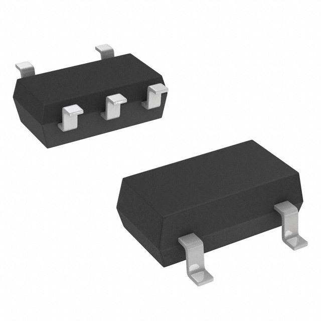
| 描述 | IC OPAMP GP 1.2MHZ RRO 14TSSOP运算放大器 - 运放 Quad 1.8V 1MHz Op Amp E temp |
| 产品分类 | Linear - Amplifiers - Instrumentation, OP Amps, Buffer Amps集成电路 - IC |
| 品牌 | Microchip Technology |
| 产品手册 | |
| 产品图片 |
|
| rohs | 符合RoHS无铅 / 符合限制有害物质指令(RoHS)规范要求 |
| 产品系列 | 放大器 IC,运算放大器 - 运放,Microchip Technology MCP6074-E/ST- |
| 数据手册 | http://www.microchip.com/mymicrochip/filehandler.aspx?ddocname=en026002http://www.microchip.com/mymicrochip/filehandler.aspx?ddocname=en540513http://www.microchip.com/mymicrochip/filehandler.aspx?ddocname=en023833 |
| 产品型号 | MCP6074-E/ST |
| PCN组件/产地 | http://www.microchip.com/mymicrochip/NotificationDetails.aspx?id=5829&print=viewhttp://www.microchip.com/mymicrochip/NotificationDetails.aspx?pcn=JAON-25KYQT864&print=view |
| 产品目录页面 | |
| 产品种类 | 运算放大器 - 运放 |
| 供应商器件封装 | 14-TSSOP |
| 共模抑制比—最小值 | 72 dB |
| 关闭 | No Shutdown |
| 其它名称 | MCP6074EST |
| 包装 | 管件 |
| 压摆率 | 0.5 V/µs |
| 商标 | Microchip Technology |
| 增益带宽生成 | 1.2 MHz |
| 增益带宽积 | 1.2MHz |
| 安装类型 | 表面贴装 |
| 安装风格 | SMD/SMT |
| 封装 | Tube |
| 封装/外壳 | 14-TSSOP(0.173",4.40mm 宽) |
| 封装/箱体 | TSSOP-14 |
| 工作温度 | -40°C ~ 125°C |
| 工作电源电压 | 1.8 V to 6 V |
| 工厂包装数量 | 96 |
| 技术 | CMOS |
| 放大器类型 | 通用 |
| 最大工作温度 | + 125 C |
| 最小工作温度 | - 40 C |
| 标准包装 | 96 |
| 电压-电源,单/双 (±) | 1.8 V ~ 6 V |
| 电压-输入失调 | 150µV |
| 电流-电源 | 110µA |
| 电流-输入偏置 | 1pA |
| 电流-输出/通道 | 28mA |
| 电源电流 | 110 uA |
| 电路数 | 4 |
| 转换速度 | 0.5 V/us |
| 输入偏压电流—最大 | 100 pA |
| 输入参考电压噪声 | 19 nV |
| 输入补偿电压 | 150 uV |
| 输出电流 | 28 mA |
| 输出类型 | 满摆幅 |
| 通道数量 | 4 Channel |


- 商务部:美国ITC正式对集成电路等产品启动337调查
- 曝三星4nm工艺存在良率问题 高通将骁龙8 Gen1或转产台积电
- 太阳诱电将投资9.5亿元在常州建新厂生产MLCC 预计2023年完工
- 英特尔发布欧洲新工厂建设计划 深化IDM 2.0 战略
- 台积电先进制程称霸业界 有大客户加持明年业绩稳了
- 达到5530亿美元!SIA预计今年全球半导体销售额将创下新高
- 英特尔拟将自动驾驶子公司Mobileye上市 估值或超500亿美元
- 三星加码芯片和SET,合并消费电子和移动部门,撤换高东真等 CEO
- 三星电子宣布重大人事变动 还合并消费电子和移动部门
- 海关总署:前11个月进口集成电路产品价值2.52万亿元 增长14.8%


PDF Datasheet 数据手册内容提取
MCP6071/2/4 110 µA, High Precision Op Amps Features Description • Low Offset Voltage: ±150µV (maximum) The Microchip Technology Inc. MCP6071/2/4 family of • Low Quiescent Current: 110µA (typical) operational amplifiers (op amps) has low input offset voltage (±150µV, maximum) and rail-to-rail input and • Rail-to-Rail Input and Output output operation. This family is unity gain stable and • Wide Supply Voltage Range: 1.8V to 6.0V has a gain bandwidth product of 1.2MHz (typical). • Gain Bandwidth Product: 1.2MHz (typical) These devices operate with a single supply voltage as • Unity Gain Stable low as 1.8V, while drawing low quiescent current per • Extended Temperature Range: -40°C to +125°C amplifier (110µA, typical). These features make the • No Phase Reversal family of op amps well suited for single-supply, high precision, battery-powered applications. Applications The MCP6071/2/4 family is offered in single (MCP6071), dual (MCP6072), and quad (MCP6074) • Automotive configurations. • Portable Instrumentation The MCP6071/2/4 is designed with Microchip’s • Sensor Conditioning advanced CMOS process. All devices are available in • Battery Powered Systems the extended temperature range, with a power supply • Medical Instrumentation range of 1.8V to 6.0V. • Test Equipment Package Types • Analog Filters MCP6071 MCP6072 Design Aids SOIC SOIC • SPICE Macro Models NC 1 8 NC VOUTA 1 8 VDD • FilterLab® Software VIN– 2 7 VDD VINA– 2 7 VOUTB • MAPS (Microchip Advanced Part Selector) VIN+ 3 6 VOUT VINA+ 3 6 VINB– • Analog Demonstration and Evaluation Boards VSS 4 5 NC VSS 4 5 VINB+ • Application Notes MCP6071 MCP6072 2x3 TDFN 2x3 TDFN Typical Application NC 1 8 NC VOUTA 1 8 VDD VIN– 2 EP 7 VDD VINA– 2 EP 7 VOUTB RL VIN+ 3 9 6 VOUT VINA+ 3 9 6 VINB– Z VOUT VSS 4 5 NC VSS 4 5 VINB+ IN MCP6071 MCP6071 MCP6074 SOT-23-5 SOIC, TSSOP C VOUT 1 5 VDD VOUTA 1 14 VOUTD ZIN = RL+jωL R VSS 2 VINA– 2 13 VIND– L = RLRC Gyrator VIN+ 3 4 VIN– VINA+ 3 12 VIND+ VDD 4 11 VSS VINB+ 5 10 VINC+ VINB– 6 9 VINC– VOUTB 7 8 VOUTC * Includes Exposed Thermal Pad (EP); see Table3-1. © 2010 Microchip Technology Inc. DS22142B-page 1
MCP6071/2/4 NOTES: DS22142B-page 2 © 2010 Microchip Technology Inc.
MCP6071/2/4 1.0 ELECTRICAL CHARACTERISTICS 1.1 Absolute Maximum Ratings † V – V ........................................................................7.0V † Notice: Stresses above those listed under “Absolute DD SS Current at Input Pins.....................................................±2mA Maximum Ratings” may cause permanent damage to the device. This is a stress rating only and functional Analog Inputs (VIN+, VIN-)††..........VSS –1.0V to VDD +1.0V operation of the device at those or any other conditions All Other Inputs and Outputs .........V –0.3V to V +0.3V SS DD above those indicated in the operational listings of this Difference Input Voltage ......................................|VDD – VSS| specification is not implied. Exposure to maximum Output Short-Circuit Current .................................continuous rating conditions for extended periods may affect Current at Output and Supply Pins ............................±30mA device reliability. Storage Temperature....................................-65°C to +150°C †† See 4.1.2 “Input Voltage Limits” Maximum Junction Temperature (T )..........................+150°C J ESD protection on all pins (HBM; MM)................≥ 4kV; 400V 1.2 Specifications TABLE 1-1: DC ELECTRICAL SPECIFICATIONS Electrical Characteristics: Unless otherwise indicated, V = +1.8V to +6.0V, V = GND, T = +25°C, V = V /2, DD SS A CM DD V ≈V /2, V = V /2 and R = 10kΩ to V . (Refer to Figure1-1). OUT DD L DD L L Parameters Sym Min Typ Max Units Conditions Input Offset Input Offset Voltage V -150 — +150 µV V = 3.0V, OS DD V = V /3 CM DD Input Offset Drift with Temperature ΔV /ΔT — ±1.5 — µV/°C T = -40°C to +85°C, OS A A V = 3.0V, V = V /3 DD CM DD ΔV /ΔT — ±4.0 — µV/°C T = +85°C to +125°C, OS A A V = 3.0V, V = V /3 DD CM DD Power Supply Rejection Ratio PSRR 70 87 — dB V = V CM SS Input Bias Current and Impedance Input Bias Current I — ±1.0 100 pA B I — 60 — pA T = +85°C B A I — 1100 5000 pA T = +125°C B A Input Offset Current I — ±1.0 — pA OS Common Mode Input Impedance Z — 1013||6 — Ω||pF CM Differential Input Impedance Z — 1013||6 — Ω||pF DIFF Common Mode Common Mode Input Voltage Range V V −0.15 — V +0.15 V V = 1.8V (Note1) CMR SS DD DD V V −0.3 — V +0.3 V V = 6.0V (Note1) CMR SS DD DD Common Mode Rejection Ratio CMRR 72 89 — dB V = -0.15V to 1.95V, CM V = 1.8V DD 74 91 — dB V = -0.3V to 6.3V, CM V = 6.0V DD 72 87 — dB V = 3.0V to 6.3V, CM V = 6.0V DD 74 89 — dB V = -0.3V to 3.0V, CM V = 6.0V DD Note 1: Figure2-13 shows how V changed across temperature. CMR © 2010 Microchip Technology Inc. DS22142B-page 3
MCP6071/2/4 TABLE 1-1: DC ELECTRICAL SPECIFICATIONS (CONTINUED) Electrical Characteristics: Unless otherwise indicated, V = +1.8V to +6.0V, V = GND, T = +25°C, V = V /2, DD SS A CM DD V ≈V /2, V = V /2 and R = 10kΩ to V . (Refer to Figure1-1). OUT DD L DD L L Parameters Sym Min Typ Max Units Conditions Open-Loop Gain DC Open-Loop Gain A 95 115 — dB 0.2V < V <(V -0.2V) OL OUT DD (Large Signal) V = V CM SS Output Maximum Output Voltage Swing V V V +15 — V –15 mV 0.5V input overdrive OL, OH SS DD Output Short-Circuit Current I — ±7 — mA V = 1.8V SC DD — ±28 — mA V = 6.0V DD Power Supply Supply Voltage V 1.8 — 6.0 V DD Quiescent Current per Amplifier I 50 110 170 µA I = 0, V = 6.0V Q O DD V = 0.9V CM DD Note 1: Figure2-13 shows how V changed across temperature. CMR TABLE 1-2: AC ELECTRICAL SPECIFICATIONS Electrical Characteristics: Unless otherwise indicated, T = +25°C, V = +1.8 to +6.0V, V = GND, V = V /2, A DD SS CM DD V ≈V /2, V = V /2, R = 10kΩ to V and C = 60pF. (Refer to Figure1-1). OUT DD L DD L L L Parameters Sym Min Typ Max Units Conditions AC Response Gain Bandwidth Product GBWP — 1.2 — MHz Phase Margin PM — 57 — ° G = +1V/V Slew Rate SR — 0.5 — V/µs Noise Input Noise Voltage E — 4.3 — µVp-p f = 0.1Hz to 10Hz ni Input Noise Voltage Density e — 19 — nV/√Hz f = 10kHz ni Input Noise Current Density i — 0.6 — fA/√Hz f = 1kHz ni TABLE 1-3: TEMPERATURE SPECIFICATIONS Electrical Characteristics: Unless otherwise indicated, V = +1.8V to +6.0V and V = GND. DD SS Parameters Sym Min Typ Max Units Conditions Temperature Ranges Operating Temperature Range T -40 — +125 °C Note1 A Storage Temperature Range T -65 — +150 °C A Thermal Package Resistances Thermal Resistance, 5L-SOT-23 θ — 220.7 — °C/W JA Thermal Resistance, 8L-2x3 TDFN θ — 52.5 — °C/W JA Thermal Resistance, 8L-SOIC θ — 149.5 — °C/W JA Thermal Resistance, 14L-SOIC θ — 95.3 — °C/W JA Thermal Resistance, 14L-TSSOP θ — 100 — °C/W JA Note1: The internal junction temperature (T ) must not exceed the absolute maximum specification of +150°C. J DS22142B-page 4 © 2010 Microchip Technology Inc.
MCP6071/2/4 1.3 Test Circuits The circuit used for most DC and AC tests is shown in Figure1-1. This circuit can independently set VCM and CF V ; see Equation1-1. Note that V is not the OUT CM 6.8pF circuit’s common mode voltage ((V +V )/2), and that P M V includes V plus the effects (on the input offset OST OS R R error, V ) of temperature, CMRR, PSRR and A . G F OST OL 100kΩ 100kΩ V V /2 EQUATION 1-1: P DD V DD V G = R ⁄R IN+ DM F G C C V = (V +V ⁄2)⁄2 B1 B2 CM P DD MCP607X 100nF 1µF V = V –V OST IN– IN+ V = (V ⁄2)+(V –V )+V (1+G ) OUT DD P M OST DM VIN– Where: V V M OUT GDM = Differential Mode Gain (V/V) RG RF RL CL VCM = Op Amp’s Common Mode (V) 100kΩ 100kΩ 10kΩ 60pF Input Voltage VOST = Op Amp’s Total Input Offset (mV) CF Voltage 6.8pF VL FIGURE 1-1: AC and DC Test Circuit for Most Specifications. © 2010 Microchip Technology Inc. DS22142B-page 5
MCP6071/2/4 NOTES: DS22142B-page 6 © 2010 Microchip Technology Inc.
MCP6071/2/4 2.0 TYPICAL PERFORMANCE CURVES Note: The graphs and tables provided following this note are a statistical summary based on a limited number of samples and are provided for informational purposes only. The performance characteristics listed herein are not tested or guaranteed. In some graphs or tables, the data presented may be outside the specified operating range (e.g., outside specified power supply range) and therefore outside the warranted range. Note: Unless otherwise indicated, T = +25°C, V = +1.8V to +6.0V, V = GND, V = V /2, V ≈V /2, A DD SS CM DD OUT DD V = V /2, R = 10kΩ to V and C = 60pF. L DD L L L 14% 1000 Occurences11028%%% 1VV2DC4DM 4 == S 3Va.D0mDV/p3les oltage (µV) 246800000000 VDD = 6.0V Representative Part ge of 6% set V -2000 Percenta 24%% Input Off ---864000000 TTTTAAAA ==== -+++42810552°°°5CCC°C 0% -1000 -150 -120 -90In-60put O-30ffset0 Volt30age (60µV) 90 120 150 -0.5 0.0 0.5Co1.0mm1.5on2.0 Mo2.5de 3.0Inp3.5ut V4.0olta4.5ge5.0 (V)5.5 6.0 6.5 FIGURE 2-1: Input Offset Voltage with FIGURE 2-4: Input Offset Voltage vs. V = 3.0V. Common Mode Input Voltage with V = 6.0V. DD DD 27% 1000 e of Occurences1112225814%%%%% 1VVT2ADC 4DM= 4 = =- S 4 3V0a.D0°mDCV/p3 tloe s+85°C set Voltage (µV) -2246800000000000 VDD = 3.0V Representative Part centag 69%% put Off --640000 TTTAAA === -++428055°°°CCC Per 3% In-1-080000 TA = +125°C 0% -20Inp-16ut O-12ffset-8 Drif-4t wit0h Tem4per8atur12e (µV16/°C)20 -0.5 -0.2 0.1Co0.4mm0.7on 1.0Mod1.3e In1.6pu1.9t Vo2.2ltag2.5e (2.8V) 3.1 3.4 FIGURE 2-2: Input Offset Voltage Drift FIGURE 2-5: Input Offset Voltage vs. with V = 3.0V and T ≤ +85°C. Common Mode Input Voltage with V = 3.0V. DD A DD 27% 1000 curences122814%%% TA = +851°2C4V 4VtC oMDS D a+=m=1 V 23pD5.lD0°e/CVs3 age (µV) 468000000 VDD = 1.8V Representative Part Oc15% olt 200 Percentage of 12369%%%% Input Offset V ----8642000000000 TTTTAAAA ==== -+++42810552°°°5CCC°C 0% -1000 -20 -16 -12 -8 -4 0 4 8 12 16 20 0.5 0.3 0.1 0.1 0.3 0.5 0.7 0.9 1.1 1.3 1.5 1.7 1.9 2.1 2.3 Input Offset Drift with Temperature (µV/°C) - - -Common Mode Input Voltage (V) FIGURE 2-3: Input Offset Voltage Drift FIGURE 2-6: Input Offset Voltage vs. with V = 3.0V and T ≥ +85°C. Common Mode Input Voltage with V = 1.8V. DD A DD © 2010 Microchip Technology Inc. DS22142B-page 7
MCP6071/2/4 Note: Unless otherwise indicated, T = +25°C, V = +1.8V to +6.0V, V = GND, V = V /2, V ≈V /2, A DD SS CM DD OUT DD V = V /2, R = 10kΩ to V and C = 60pF. L DD L L L 350 y 40 age (µV) 125500 Representative Part e Densit 3305 fV =DD 1 =0 6k.H0zV et Volt -5500 VDD = 6.0V VoltagV/Hz)√2205 Input Offs---321555000 VDD = 1.8V VDD = 3.0V Input Noise (n110505 0.0 0.5 1.0 1.5 2.0 2.5 3.0 3.5 4.0 4.5 5.0 5.5 6.0 0.5 0.0 0.5 1.0 1.5 2.0 2.5 3.0 3.5 4.0 4.5 5.0 5.5 6.0 6.5 Output Voltage (V) - Common Mode Input Voltage (V) FIGURE 2-7: Input Offset Voltage vs. FIGURE 2-10: Input Noise Voltage Density Output Voltage. vs. Common Mode Input Voltage. 1000 110 V) 800 TA = -40°C Representative Part 100 PSRR- Representative Part ge (µ 460000 TTAA == ++2855°°CC dB)90 CMRR Offset Volta --2420000000 TA = +125°C RR, PSRR (56780000 PSRR+ ut -600 CM40 Inp-1-080000 30 5 0 5 0 5 0 5 0 5 0 5 20 1. 2. 2. 3. 3. 4. 4. 5. 5. 6. 6. 1100 110000 1 10k00 1 10000k0 1 1000000k0 1 010M0000 Power Supply Voltage (V) Frequency (Hz) FIGURE 2-8: Input Offset Voltage vs. FIGURE 2-11: CMRR, PSRR vs. Power Supply Voltage. Frequency. 1,000 110 sity 105 CMRR (VDD = 6.0V, VCM = -0.3V to 6.3V) en B)100 D d 95 e Voltage nV/Hz)√100 R, CMRR ( 889050 PSRR (VDD = 1.8V to 6.0V, VCM = VSS) ois( SR 75 N P 70 ut 65 p In 10 60 1 .0E.-11 1 .1E + 0 110.E + 1 101.0E + 2 11k. E + 3 101k.E + 4 1001k.E+5 -50 -25 0 25 50 75 100 125 Ambient Temperature (°C) Frequency (Hz) FIGURE 2-9: Input Noise Voltage Density FIGURE 2-12: CMRR, PSRR vs. Ambient vs. Frequency. Temperature. DS22142B-page 8 © 2010 Microchip Technology Inc.
MCP6071/2/4 Note: Unless otherwise indicated, T = +25°C, V = +1.8V to +6.0V, V = GND, V = V /2, V ≈V /2, A DD SS CM DD OUT DD V = V /2, R = 10kΩ to V and C = 60pF. L DD L L L e 00..3305 150 ag 0.25 140 mon Mode Input VoltRange Limit (V)----000000000.........211000112050505050 V C M R _ H V- VC M DVV R D@@OO_ @LLL ---VV VVVVDDDDDSSS DSSS== @@@= 31 6.. 08VVV.0VVDDDVDDD === 136...800VVV Quiescent Current (µA/Amplifier)1111012389000000 VVDCDM == 60..09VV DD VDD = 1.8V Com --00..3205 70 VCM = 0.9VDD -0.35 60 -50 -25 0 25 50 75 100 125 -50 -25 0 25 50 75 100 125 Ambient Temperature (°C) Ambient Temperature (°C) FIGURE 2-13: Common Mode Input FIGURE 2-16: Quiescent Current vs Voltage Range Limit vs. Ambient Temperature. Ambient Temperature with V = 0.9V . CM DD 10000 180 Input Bias and Offset Currents (pA) 110001000 VVDCDM == 6VI.nD0DpVut Bias CurrentInput Offset Current Quiescent Current (µA/Amplifier)11112468024600000000 VVDCDM == 60..09VV DD TTTTAAAA ==== +++-41820255°5°°CCC°C 1 0 0 5 0 5 0 5 0 5 0 5 0 5 0 5 0 25 45 65 85 105 125 0. 0. 1. 1. 2. 2. 3. 3. 4. 4. 5. 5. 6. 6. 7. Ambient Temperature (°C) Power Supply Voltage (V) FIGURE 2-14: Input Bias, Offset Currents FIGURE 2-17: Quiescent Current vs. vs. Ambient Temperature. Power Supply Voltage with V = 0.9V . CM DD 10000 120 0 A) VDD = 6.0V 100 Open-Loop Gain -30 Bias Current (p 1010000 TA = +125°C Loop Gain (dB) 468000 Open-Loop Phase ---1962000Loop Phase (°) Input 10 TA = +85°C Open- 200 VDD = 6.0V --118500Open- 1 0.0 0.5 1.0 1.5 2.0 2.5 3.0 3.5 4.0 4.5 5.0 5.5 6.0 -20 -210 1 0.E.-101 1 . E1+ 0 0 11.E0+ 0 1 11.0E0+0 2 11.Ek+ 0 3 110.Ek+0 4 110.E0+0k5 1 1.EM+0 6 11.E0+M07 Common Mode Input Votlage (V) FFrreeqquueennccyy ((HHzz)) FIGURE 2-15: Input Bias Current vs. FIGURE 2-18: Open-Loop Gain, Phase vs. Common Mode Input Voltage. Frequency. © 2010 Microchip Technology Inc. DS22142B-page 9
MCP6071/2/4 Note: Unless otherwise indicated, T = +25°C, V = +1.8V to +6.0V, V = GND, V = V /2, V ≈V /2, A DD SS CM DD OUT DD V = V /2, R = 10kΩ to V and C = 60pF. L DD L L L 150 1.8 180 B)145 uct 1.6 Gain Bandwidth Product 160 DC-Open-Loop Gain (d111111110112233450505050 RVSL S= + 1 00. 2kVΩ < VOUT < VDD - 0.2V Gain Bandwidth Prod(MHz)00000111........02468024 VDD = 6.0V Phase Margin 024681110000024000Phase Margin (°) 100 505050505050505 1.5 2.0 2.5 3.0 3.5 4.0 4.5 5.0 5.5 6.0 -0.0.0.1.1.2.2.3.3.4.4.5.5.6.6. Power Supply Voltage (V) Common Mode Input Voltage (V) FIGURE 2-19: DC Open-Loop Gain vs. FIGURE 2-22: Gain Bandwidth Product, Power Supply Voltage. Phase Margin vs. Common Mode Input Voltage. 150 1.8 180 en-Loop Gain (dB)111111112233445050505 VDD = 6.0VVDD = 1.8V ndwidth Product (MHz)01111.....80246 Gain Bandwidth Product 81111002460000 se Margin (°) Op110 Ba 0.6 60 ha DC-110005 Large Signal AOL Gain 00..24 VDD = 6.0V Phase Margin 2400 P 0.00 0.05 0.10 0.15 0.20 0.25 0.0 0 Output Voltage Headroom -50 -25 0 25 50 75 100 125 VDD - VOH or VOL - VSS (V) Ambient Temperature (°C) FIGURE 2-20: DC Open-Loop Gain vs. FIGURE 2-23: Gain Bandwidth Product, Output Voltage Headroom. Phase Margin vs. Ambient Temperature. 150 1.8 180 Channel to Channel Separation (dB)11111012349000000 Input Referred ain Bandwidth Product (MHz)0001111.......4680246 VDD =G 1a.8inV BandwidtPh hParsoed Mucatrgin 468111100002460000Phase Margin (°) G 0.2 20 80 0.0 0 1 . 0 01E00+ 0 2 1 . 010kE + 0 3 1 .1000kE + 0 4 11.0000kE + 0 5 11M.00E+06 -50 -25 0 25 50 75 100 125 Frequency (Hz) Ambient Temperature (°C) FIGURE 2-21: Channel-to-Channel FIGURE 2-24: Gain Bandwidth Product, Separation vs. Frequency ( MCP6072/4 only). Phase Margin vs. Ambient Temperature. DS22142B-page 10 © 2010 Microchip Technology Inc.
MCP6071/2/4 Note: Unless otherwise indicated, T = +25°C, V = +1.8V to +6.0V, V = GND, V = V /2, V ≈V /2, A DD SS CM DD OUT DD V = V /2, R = 10kΩ to V and C = 60pF. L DD L L L nt 40 16.0 urre 35 TA = -40°C ommV) 14.0 Output Short Circuit C(mA)112230505005 TTTAAA === +++281552°°5CC°C Output Voltage HeadroV - V or V - V (DDOHOLSS11022468......000000 VOL -V VDDS S- VOH 0 5 0 5 0 5 0 5 0 5 0 5 0 0.0 0. 0. 1. 1. 2. 2. 3. 3. 4. 4. 5. 5. 6. -50 -25 0 25 50 75 100 125 Power Supply Voltage (V) Ambient Temperature (°C) FIGURE 2-25: Ouput Short Circuit Current FIGURE 2-28: Output Voltage Headroom vs. Power Supply Voltage. vs. Ambient Temperature. 1.0 10 ng (V)P-P VDD = 6.0V VDD = 1.8V µs)000...789 FFaalllliinngg EEddggee,, VVDDDD == 61..08VV wi V/0.6 ut Voltage S 1 Slew Rate (0000....2345 Rising Edge, VDD = 6.0V utp 0.1 Rising Edge, VDD = 1.8V O 0.1 0.0 1 10k0 0 1 10000k0 1 0 1000000k 1 0 0 010M00 -50 -25 0 25 50 75 100 125 Frequency (Hz) Ambient Temperature (°C) FIGURE 2-26: Output Voltage Swing vs. FIGURE 2-29: Slew Rate vs. Ambient Frequency. Temperature. m to 5650 (VDD - VOH)/IOUT VDD = 1.8V v) o of Output HeadrooCurrent (mV/mA)112233445050505050 (VDD - VOH)/IOUT ((VVOOLL -- VVSSSS))//((--IIOOUUTT)) VDD = 6.0V put Voltage (50 mV/di VGD =D =+ 16 .V0/VV Rati 05 Out 0.1 1 10 Output Current (mA) Time (2 µs/div) FIGURE 2-27: Ratio of Output Voltage FIGURE 2-30: Small Signal Non-Inverting Headroom to Output Current vs. Output Current. Pulse Response. © 2010 Microchip Technology Inc. DS22142B-page 11
MCP6071/2/4 Note: Unless otherwise indicated, T = +25°C, V = +1.8V to +6.0V, V = GND, V = V /2, V ≈V /2, A DD SS CM DD OUT DD V = V /2, R = 10kΩ to V and C = 60pF. L DD L L L 7.0 mV/div) VGD =D =-1 6 V.0/VV V) 56..00 VOUT 50 ge ( 4.0 VIN ge ( olta 3.0 a V Volt put 2.0 put Out 1.0 ut O 0.0 VDD = 6.0V G = +2 V/V -1.0 Time (2 µs/div) Time (0.1 ms/div) FIGURE 2-31: Small Signal Inverting Pulse FIGURE 2-34: The MCP6071/2/4 Shows Response. No Phase Reversal. 6.0 1000 5.5 5.0 ut oltage (V)3344....0505 oop Outpance (Ω)100 V Ld Output 122...505 VDD = 6.0V Closed Impe 10 G1101N1 :V V/V/V 1.0 G = +1 V/V 1 V/V 0.5 1 0.0 1100 110000 1 10k00 1 01000k0 1 1000000k0 1 0 10M0000 Time (0.02 ms/div) Frequency (Hz) FIGURE 2-32: Large Signal Non-Inverting FIGURE 2-35: Closed Loop Output Pulse Response. Impedance vs. Frequency. 6.0 1.1E-m03 5.5 110.E0-0µ4 V)45..50 VGD =D =-1 6 V.0/VV 11.E0-0µ5 e (4.0 1.E1-0µ6 ag3.5 A) 110.E0-0n7 utput Volt1223....5050 -I (IN 111101...EEE001---100nnp098 TTTTAAAA ==== -+++42810552°°°5CCC°C O 1.0 11.E0-1p1 0.5 1.E1-1p2 0.0 -1.0 -0.9 -0.8 -0.7 -0.6 -0.5 -0.4 -0.3 -0.2 -0.1 0.0 Time (0.02 ms/div) V (V) IN FIGURE 2-33: Large Signal Inverting Pulse FIGURE 2-36: Measured Input Current vs. Response. Input Voltage (below V ). SS DS22142B-page 12 © 2010 Microchip Technology Inc.
MCP6071/2/4 3.0 PIN DESCRIPTIONS Descriptions of the pins are listed in Table3-1. TABLE 3-1: PIN FUNCTION TABLE MCP6071 MCP6072 MCP6074 SOIC, Symbol Description SOIC SOT-23-5 2x3 TDFN SOIC 2x3 TDFN TSSOP 6 1 6 1 1 1 V , V Analog Output (op amp A) OUT OUTA 2 4 2 2 2 2 V –, V – Inverting Input (op amp A) IN INA 3 3 3 3 3 3 V +, V + Non-inverting Input (op amp A) IN INA 7 5 7 8 8 4 V Positive Power Supply DD — — — 5 5 5 V + Non-inverting Input (op amp B) INB — — — 6 6 6 V – Inverting Input (op amp B) INB — — — 7 7 7 V Analog Output (op amp B) OUTB — — — — — 8 V Analog Output (op amp C) OUTC — — — — — 9 V – Inverting Input (op amp C) INC — — — — — 10 V + Non-inverting Input (op amp C) INC 4 2 4 4 4 11 V Negative Power Supply SS — — — — — 12 V + Non-inverting Input (op amp D) IND — — — — — 13 V – Inverting Input (op amp D) IND — — — — — 14 V Analog Output (op amp D) OUTD 1, 5, 8 — 1, 5, 8 — — — NC No Internal Connection — — 9 — 9 — EP Exposed Thermal Pad (EP); must be connected to V . SS 3.1 Analog Outputs 3.3 Power Supply Pins The output pins are low-impedance voltage sources. The positive power supply (V ) is 1.8V to 6.0V higher DD than the negative power supply (V ). For normal SS 3.2 Analog Inputs operation, the other pins are at voltages between VSS and V . DD The non-inverting and inverting inputs are high- Typically, these parts are used in a single (positive) impedance CMOS inputs with low bias currents. supply configuration. In this case, V is connected to SS ground and V is connected to the supply. V will DD DD need bypass capacitors. 3.4 Exposed Thermal Pad (EP) There is an internal electrical connection between the Exposed Thermal Pad (EP) and the V pin; they must SS be connected to the same potential on the Printed Circuit Board (PCB). © 2010 Microchip Technology Inc. DS22142B-page 13
MCP6071/2/4 NOTES: DS22142B-page 14 © 2010 Microchip Technology Inc.
MCP6071/2/4 4.0 APPLICATION INFORMATION V DD The MCP6071/2/4 family of op amps is manufactured using Microchip’s state-of-the-art CMOS process and is specifically designed for low-power, high precision D1 D2 U1 applications. V 1 4.1 Rail-to-Rail Input MCP607X V V OUT 2 4.1.1 PHASE REVERSAL The MCP6071/2/4 op amps are designed to prevent FIGURE 4-2: Protecting the Analog phase reversal when the input pins exceed the supply Inputs. voltages. Figure2-34 shows the input voltage A significant amount of current can flow out of the exceeding the supply voltage without any phase inputs when the Common Mode voltage (V ) is below reversal. CM ground (V ). See Figure2-36. SS 4.1.2 INPUT VOLTAGE LIMITS 4.1.3 INPUT CURRENT LIMITS In order to prevent damage and/or improper operation In order to prevent damage and/or improper operation of these amplifiers, the circuit must limit the voltages at of these amplifiers, the circuit must limit the voltages at the input pins (see Section1.1, Absolute Maximum the input pins (see Section1.1, Absolute Maximum Ratings †). Ratings †). The ESD protection on the inputs can be depicted as Figure4-3 shows one approach to protecting these shown in Figure4-1. This structure was chosen to inputs. The resistors R and R limit the possible cur- protect the input transistors and to minimize input bias 1 2 rents in or out of the input pins (and the ESD diodes, D current (I ). 1 B and D ). The diode currents will go through either V 2 DD or V . SS Bond V DD V Pad DD D1 D2 U1 Bond Input Bond VIN+ Pad Stage Pad VIN– V1 V R OUT 1 MCP607X V 2 Bond R V 2 SS Pad VSS–min (V1,V2) min(R ,R )> 1 2 2mA FIGURE 4-1: Simplified Analog Input ESD max(V ,V )–V 1 2 DD min(R ,R )> Structures. 1 2 2mA FIGURE 4-3: Protecting the Analog The input ESD diodes clamp the inputs when they try Inputs. to go more than one diode drop below V . They also SS clamp any voltages that go well above V ; their break- DD 4.1.4 NORMAL OPERATION down voltage is high enough to allow normal operation, but not low enough to protect against slow over-voltage The input stage of the MCP6071/2/4 op amps use two (beyond V ) events. Very fast ESD events (that meet differential input stages in parallel. One operates at a DD the spec) are limited so that damage does not occur. low common mode input voltage (V ), while the other CM operates at a high V . With this topology, the device In some applications, it may be necessary to prevent CM operates with a V up to 300mV above V and excessive voltages from reaching the op amp inputs. CM DD 300mV below V . (See Figure2-13). The input offset Figure4-2 shows one approach to protecting these SS voltage is measured at V = V –0.3V and inputs. CM SS V +0.3V to ensure proper operation. DD The transition between the input stages occurs when V is near V –1.1V (See Figures2-4,2-5 and CM DD Figure2-6). For the best distortion performance and gain linearity, with non-inverting gains, avoid this region of operation. © 2010 Microchip Technology Inc. DS22142B-page 15
MCP6071/2/4 4.2 Rail-to-Rail Output After selecting R for your circuit, double-check the ISO resulting frequency response peaking and step The output voltage range of the MCP6071/2/4 op amps response overshoot. Modify R ’s value until the ISO is VSS+15mV (minimum) and VDD – 15mV response is reasonable. Bench evaluation and (maximum) when RL=10kΩ is connected to VDD/2 simulations with the MCP6071/2/4 SPICE macro and VDD=6.0V. Refer to Figures2-27 and 2-28 for model are very helpful. more information. 4.4 Supply Bypass 4.3 Capacitive Loads With this family of operational amplifiers, the power Driving large capacitive loads can cause stability supply pin (V for single-supply) should have a local problems for voltage feedback op amps. As the load DD bypass capacitor (i.e., 0.01µF to 0.1µF) within 2mm capacitance increases, the feedback loop’s phase for good high frequency performance. It can use a bulk margin decreases and the closed-loop bandwidth is capacitor (i.e., 1µF or larger) within 100mm to provide reduced. This produces gain peaking in the frequency large, slow currents. This bulk capacitor can be shared response, with overshoot and ringing in the step with other analog parts. response. While a unity-gain buffer (G = +1) is the most sensitive to capacitive loads, all gains show the same 4.5 Unused Op Amps general behavior. When driving large capacitive loads with these op An unused op amp in a quad package (MCP6074) amps (e.g., > 100pF when G = +1), a small series should be configured as shown in Figure4-6. These resistor at the output (R in Figure4-4) improves the circuits prevent the output from toggling and causing ISO feedback loop’s phase margin (stability) by making the crosstalk. Circuit A sets the op amp at its minimum output load resistive at higher frequencies. The noise gain. The resistor divider produces any desired bandwidth will be generally lower than the bandwidth reference voltage within the output voltage range of the with no capacitance load. op amp; the op amp buffers that reference voltage. Circuit B uses the minimum number of components and operates as a comparator, but it may draw more current. – RISO MCP607X VOUT ¼ MCP6074 (A) ¼ MCP6074 (B) V + IN CL VDD VDD V R DD 1 FIGURE 4-4: Output Resistor, R ISO Stabilizes Large Capacitive Loads. V R REF 2 Figure4-5 gives recommended R values for ISO different capacitive loads and gains. The x-axis is the normalized load capacitance (C /G ), where G is the L N N R 2 circuit's noise gain. For non-inverting gains, GN and the VREF = VDD×R---------+------R----- Signal Gain are equal. For inverting gains, GN is 1 2 1+|Signal Gain| (e.g., -1V/V gives G = +2V/V). N FIGURE 4-6: Unused Op Amps. 1000 (Ω)O VRDLD = = 1 60. 0k ΩV S R I 100 d e nd GN: e 1 V/V m 10 2 V/V m o ≥ 5 V/V c e R 1 11.0Ep-1 1 1 .1E0-100p 1 .1En-0 9 1 1.E0-n0 8 1 0.E.1-0µ7 1 .1Eµ-0 6 Normalized Load Capacitance; C/G (F) L N FIGURE 4-5: Recommended R Values ISO for Capacitive Loads. DS22142B-page 16 © 2010 Microchip Technology Inc.
MCP6071/2/4 4.6 PCB Surface Leakage In applications where low input bias current is critical, Printed Circuit Board (PCB) surface leakage effects need to be considered. Surface leakage is caused by humidity, dust or other contamination on the board. Under low humidity conditions, a typical resistance between nearby traces is 1012Ω. A 5V difference would cause 5pA of current to flow; which is greater than the MCP6071/2/4 family’s bias current at +25°C (±1.0pA, typical). The easiest way to reduce surface leakage is to use a guard ring around sensitive pins (or traces). The guard ring is biased at the same voltage as the sensitive pin. An example of this type of layout is shown in Figure4-7. Guard Ring V – V + V IN IN SS FIGURE 4-7: Example Guard Ring Layout for Inverting Gain. 1. Non-inverting Gain and Unity-Gain Buffer: a.Connect the non-inverting pin (V +) to the IN input with a wire that does not touch the PCB surface. b.Connect the guard ring to the inverting input pin (V –). This biases the guard ring to the IN common mode input voltage. 2. Inverting Gain and Transimpedance Gain Amplifiers (convert current to voltage, such as photo detectors): a.Connect the guard ring to the non-inverting input pin (V +). This biases the guard ring IN to the same reference voltage as the op amp (e.g., V /2 or ground). DD b.Connect the inverting pin (V –) to the input IN with a wire that does not touch the PCB surface. © 2010 Microchip Technology Inc. DS22142B-page 17
MCP6071/2/4 4.7 Application Circuits 4.7.2 INSTRUMENTATION AMPLIFIER The MCP6071/2/4 op amps are well suited for 4.7.1 GYRATOR conditioning sensor signals in battery-powered The MCP6071/2/4 op amps can be used in gyrator applications. Figure4-9 shows a two op amp applications. The gyrator is an electric circuit which can instrumentation amplifier, using the MCP6072, that make a capacitive circuit behave inductively. works well for applications requiring rejection of common mode noise at higher gains. The reference Figure4-8 shows an example of a gyrator simulating voltage (V ) is supplied by a low impedance source. inductance, with an approximately equivalent circuit REF In single supply applications, V is typically V /2. below. The two Z have similar values in typical REF DD IN applications. The primary application for a gyrator is to reduce the size and cost of a system by removing the RG need for bulky, heavy and expensive inductors. For example, RLC bandpass filter characteristics can be VREF R1 R2 R2 R1 VOUT realized with capacitors, resistors and operational amplifiers without using inductors. Moreover, gyrators will typically have higher accuracy than real inductors, V 2 due to the lower cost of precision capacitors than ½ ½ inductors. MCP6072 MCP6072 . V1 R L R 2R V = (V –V )⎛1+----1--+--------1-⎞ +V Z VOUT OUT 1 2 ⎝ R2 RG⎠ REF IN MCP6071 FIGURE 4-9: Two Op Amp Instrumentation Amplifier. C Gyrator To obtain the best CMRR possible, and not limit the R Z = R +jωL performance by the resistor tolerances, set a high gain IN L with the R resistor. G L = R RC L 4.7.3 PRECISION COMPARATOR R Z L IN Use high gain before a comparator to improve the latter’s input offset performance. Figure4-10 shows a Equivalent Circuit gain of 11V/V placed before a comparator. The L reference voltage V can be any value between the REF supply rails. FIGURE 4-8: Gyrator. V IN MCP6071 1MΩ MCP6541 V 100kΩ OUT V REF FIGURE 4-10: Precision, Non-inverting Comparator. DS22142B-page 18 © 2010 Microchip Technology Inc.
MCP6071/2/4 5.0 DESIGN AIDS 5.4 Analog Demonstration and Evaluation Boards Microchip provides the basic design tools needed for the MCP6071/2/4 family of op amps. Microchip offers a broad spectrum of Analog Demonstration and Evaluation Boards that are 5.1 SPICE Macro Model designed to help you achieve faster time to market. For a complete listing of these boards and their The latest SPICE macro model for the MCP6071/2/4 corresponding user’s guides and technical information, op amps is available on the Microchip web site at visit the Microchip web site at www.microchip.com/ www.microchip.com. The model was written and tested analogtools. in official Orcad (Cadence) owned PSPICE. For the Some boards that are especially useful are: other simulators, it may require translation. • MCP6XXX Amplifier Evaluation Board 1 The model covers a wide aspect of the op amp's electrical specifications. Not only does the model cover • MCP6XXX Amplifier Evaluation Board 2 voltage, current, and resistance of the op amp, but it • MCP6XXX Amplifier Evaluation Board 3 also covers the temperature and noise effects on the • MCP6XXX Amplifier Evaluation Board 4 behavior of the op amp. The model has not been • Active Filter Demo Board Kit verified outside of the specification range listed in the • 5/6-Pin SOT-23 Evaluation Board, P/N VSUPEV2 op amp data sheet. The model behaviors under these • 8-Pin SOIC/MSOP/TSSOP/DIP Evaluation Board, conditions can not be guaranteed that it will match the P/N SOIC8EV actual op amp performance. • 14-Pin SOIC/TSSOP/DIP Evaluation Board, P/N Moreover, the model is intended to be an initial design SOIC14EV tool. Bench testing is a very important part of any design and cannot be replaced with simulations. Also, 5.5 Application Notes simulation results using this macro model need to be validated by comparing them to the data sheet The following Microchip Analog Design Note and specifications and characteristic curves. Application Notes are available on the Microchip web site at www.microchip. com/appnotes and are 5.2 FilterLab® Software recommended as supplemental reference resources. Microchip’s FilterLab® software is an innovative • ADN003: “Select the Right Operational Amplifier software tool that simplifies analog active filter (using for your Filtering Circuits”, DS21821 op amps) design. Available at no cost from the • AN722: “Operational Amplifier Topologies and DC Microchip web site at www.microchip.com/filterlab, the Specifications”, DS00722 FilterLab design tool provides full schematic diagrams • AN723: “Operational Amplifier AC Specifications of the filter circuit with component values. It also and Applications”, DS00723 outputs the filter circuit in SPICE format, which can be • AN884: “Driving Capacitive Loads With Op used with the macro model to simulate actual filter Amps”, DS00884 performance. • AN990: “Analog Sensor Conditioning Circuits– An Overview”, DS00990 5.3 MAPS (Microchip Advanced Part • AN1177: “Op Amp Precision Design: DC Errors”, Selector) DS01177 MAPS is a software tool that helps semiconductor • AN1228: “Op Amp Precision Design: Random professionals efficiently identify Microchip devices that Noise”, DS01228 fit a particular design requirement. Available at no cost • AN1332: “Current Sensing Circuit Concepts and from the Microchip website at www.microchip.com/ Fundamentals”, DS01332 maps, the MAPS is an overall selection tool for These application notes and others are listed in the Microchip’s product portfolio that includes Analog, design guide: Memory, MCUs and DSCs. Using this tool you can define a filter to sort features for a parametric search of • “Signal Chain Design Guide”, DS21825 devices and export side-by-side technical comparison reports. Helpful links are also provided for Data Sheets, purchase, and sampling of Microchip parts. © 2010 Microchip Technology Inc. DS22142B-page 19
MCP6071/2/4 NOTES: DS22142B-page 20 © 2010 Microchip Technology Inc.
MCP6071/2/4 6.0 PACKAGING INFORMATION 6.1 Package Marking Information 5-Lead SOT-23 (MCP6071) Example: XXNN YH25 8-Lead SOIC (150 mil) (MCP6071, MCP6072) Example: XXXXXXXX MCP6071E XXXXYYWW SN^e^31044 NNN 256 8-Lead 2x3 TDFN (MCP6071, MCP6072) Example: XXX AHE YWW 044 NN 25 Legend: XX...X Customer-specific information Y Year code (last digit of calendar year) YY Year code (last 2 digits of calendar year) WW Week code (week of January 1 is week ‘01’) NNN Alphanumeric traceability code e3 Pb-free JEDEC designator for Matte Tin (Sn) * This package is Pb-free. The Pb-free JEDEC designator ( e 3 ) can be found on the outer packaging for this package. Note: In the event the full Microchip part number cannot be marked on one line, it will be carried over to the next line, thus limiting the number of available characters for customer-specific information. © 2010 Microchip Technology Inc. DS22142B-page 21
MCP6071/2/4 Package Marking Information (Continuation) 14-Lead SOIC (150 mil) (MCP6074) Example: XXXXXXXXXXX MCP6074 XXXXXXXXXXX E/SL e3 YYWWNNN 1044256 14-Lead TSSOP (MCP6074) Example: XXXXXXXX MCP6074E YYWW 1044 256 NNN DS22142B-page 22 © 2010 Microchip Technology Inc.
MCP6071/2/4 (cid:2)(cid:3)(cid:4)(cid:5)(cid:6)(cid:7)(cid:8)(cid:9)(cid:10)(cid:6)(cid:11)(cid:12)(cid:13)(cid:14)(cid:8)(cid:15)(cid:16)(cid:6)(cid:10)(cid:10)(cid:8)(cid:17)(cid:18)(cid:12)(cid:10)(cid:13)(cid:19)(cid:5)(cid:8)(cid:20)(cid:21)(cid:6)(cid:19)(cid:11)(cid:13)(cid:11)(cid:12)(cid:22)(cid:21)(cid:8)(cid:23)(cid:17)(cid:20)(cid:24)(cid:8)(cid:25)(cid:15)(cid:17)(cid:20)(cid:3)(cid:26)(cid:27)(cid:28) (cid:29)(cid:22)(cid:12)(cid:5)(cid:30) .(cid:22)(cid:21)(cid:14)#(cid:23)(cid:13)(cid:14)(cid:31)(cid:22) #(cid:14)(cid:20)$(cid:21)(cid:21)(cid:13)(cid:25)#(cid:14)(cid:10)(cid:11)(cid:20)/(cid:11)(cid:12)(cid:13)(cid:14)!(cid:21)(cid:11)-(cid:19)(cid:25)(cid:12) 0(cid:14)(cid:10)(cid:26)(cid:13)(cid:11) (cid:13)(cid:14) (cid:13)(cid:13)(cid:14)#(cid:23)(cid:13)(cid:14)(cid:18)(cid:19)(cid:20)(cid:21)(cid:22)(cid:20)(cid:23)(cid:19)(cid:10)(cid:14)1(cid:11)(cid:20)/(cid:11)(cid:12)(cid:19)(cid:25)(cid:12)(cid:14)(cid:3)(cid:10)(cid:13)(cid:20)(cid:19)%(cid:19)(cid:20)(cid:11)#(cid:19)(cid:22)(cid:25)(cid:14)(cid:26)(cid:22)(cid:20)(cid:11)#(cid:13)!(cid:14)(cid:11)#(cid:14) (cid:23)##(cid:10)+22---(cid:29)(cid:31)(cid:19)(cid:20)(cid:21)(cid:22)(cid:20)(cid:23)(cid:19)(cid:10)(cid:29)(cid:20)(cid:22)(cid:31)2(cid:10)(cid:11)(cid:20)/(cid:11)(cid:12)(cid:19)(cid:25)(cid:12) b N E E1 1 2 3 e e1 D A A2 c φ A1 L L1 3(cid:25)(cid:19)# (cid:18)(cid:28)44(cid:28)(cid:18)"(cid:24)"(cid:8)(cid:3) (cid:2)(cid:19)(cid:31)(cid:13)(cid:25) (cid:19)(cid:22)(cid:25)(cid:14)4(cid:19)(cid:31)(cid:19)# (cid:18)(cid:28)5 56(cid:18) (cid:18)(cid:7)7 5$(cid:31)8(cid:13)(cid:21)(cid:14)(cid:22)%(cid:14)1(cid:19)(cid:25) 5 ( 4(cid:13)(cid:11)!(cid:14)1(cid:19)#(cid:20)(cid:23) (cid:13) (cid:4)(cid:29)(cid:6)((cid:14))(cid:3)* 6$# (cid:19)!(cid:13)(cid:14)4(cid:13)(cid:11)!(cid:14)1(cid:19)#(cid:20)(cid:23) (cid:13)(cid:30) (cid:30)(cid:29)(cid:6)(cid:4)(cid:14))(cid:3)* 6,(cid:13)(cid:21)(cid:11)(cid:26)(cid:26)(cid:14)9(cid:13)(cid:19)(cid:12)(cid:23)# (cid:7) (cid:4)(cid:29)(cid:6)(cid:4) : (cid:30)(cid:29)(cid:5)( (cid:18)(cid:22)(cid:26)!(cid:13)!(cid:14)1(cid:11)(cid:20)/(cid:11)(cid:12)(cid:13)(cid:14)(cid:24)(cid:23)(cid:19)(cid:20)/(cid:25)(cid:13) (cid:7)(cid:16) (cid:4)(cid:29);(cid:6) : (cid:30)(cid:29)(cid:15)(cid:4) (cid:3)#(cid:11)(cid:25)!(cid:22)%% (cid:7)(cid:30) (cid:4)(cid:29)(cid:4)(cid:4) : (cid:4)(cid:29)(cid:30)( 6,(cid:13)(cid:21)(cid:11)(cid:26)(cid:26)(cid:14)<(cid:19)!#(cid:23) " (cid:16)(cid:29)(cid:16)(cid:4) : (cid:15)(cid:29)(cid:16)(cid:4) (cid:18)(cid:22)(cid:26)!(cid:13)!(cid:14)1(cid:11)(cid:20)/(cid:11)(cid:12)(cid:13)(cid:14)<(cid:19)!#(cid:23) "(cid:30) (cid:30)(cid:29)(cid:15)(cid:4) : (cid:30)(cid:29);(cid:4) 6,(cid:13)(cid:21)(cid:11)(cid:26)(cid:26)(cid:14)4(cid:13)(cid:25)(cid:12)#(cid:23) (cid:2) (cid:16)(cid:29)(cid:17)(cid:4) : (cid:15)(cid:29)(cid:30)(cid:4) .(cid:22)(cid:22)#(cid:14)4(cid:13)(cid:25)(cid:12)#(cid:23) 4 (cid:4)(cid:29)(cid:30)(cid:4) : (cid:4)(cid:29)=(cid:4) .(cid:22)(cid:22)#(cid:10)(cid:21)(cid:19)(cid:25)# 4(cid:30) (cid:4)(cid:29)(cid:15)( : (cid:4)(cid:29);(cid:4) .(cid:22)(cid:22)#(cid:14)(cid:7)(cid:25)(cid:12)(cid:26)(cid:13) (cid:3) (cid:4)> : (cid:15)(cid:4)> 4(cid:13)(cid:11)!(cid:14)(cid:24)(cid:23)(cid:19)(cid:20)/(cid:25)(cid:13) (cid:20) (cid:4)(cid:29)(cid:4); : (cid:4)(cid:29)(cid:16)= 4(cid:13)(cid:11)!(cid:14)<(cid:19)!#(cid:23) 8 (cid:4)(cid:29)(cid:16)(cid:4) : (cid:4)(cid:29)((cid:30) (cid:29)(cid:22)(cid:12)(cid:5)(cid:11)(cid:30) (cid:30)(cid:29) (cid:2)(cid:19)(cid:31)(cid:13)(cid:25) (cid:19)(cid:22)(cid:25) (cid:14)(cid:2)(cid:14)(cid:11)(cid:25)!(cid:14)"(cid:30)(cid:14)!(cid:22)(cid:14)(cid:25)(cid:22)#(cid:14)(cid:19)(cid:25)(cid:20)(cid:26)$!(cid:13)(cid:14)(cid:31)(cid:22)(cid:26)!(cid:14)%(cid:26)(cid:11) (cid:23)(cid:14)(cid:22)(cid:21)(cid:14)(cid:10)(cid:21)(cid:22)#(cid:21)$ (cid:19)(cid:22)(cid:25) (cid:29)(cid:14)(cid:18)(cid:22)(cid:26)!(cid:14)%(cid:26)(cid:11) (cid:23)(cid:14)(cid:22)(cid:21)(cid:14)(cid:10)(cid:21)(cid:22)#(cid:21)$ (cid:19)(cid:22)(cid:25) (cid:14) (cid:23)(cid:11)(cid:26)(cid:26)(cid:14)(cid:25)(cid:22)#(cid:14)(cid:13)&(cid:20)(cid:13)(cid:13)!(cid:14)(cid:4)(cid:29)(cid:30)(cid:16)(cid:17)(cid:14)(cid:31)(cid:31)(cid:14)(cid:10)(cid:13)(cid:21)(cid:14) (cid:19)!(cid:13)(cid:29) (cid:16)(cid:29) (cid:2)(cid:19)(cid:31)(cid:13)(cid:25) (cid:19)(cid:22)(cid:25)(cid:19)(cid:25)(cid:12)(cid:14)(cid:11)(cid:25)!(cid:14)#(cid:22)(cid:26)(cid:13)(cid:21)(cid:11)(cid:25)(cid:20)(cid:19)(cid:25)(cid:12)(cid:14)(cid:10)(cid:13)(cid:21)(cid:14)(cid:7)(cid:3)(cid:18)"(cid:14)’(cid:30)(cid:5)(cid:29)((cid:18)(cid:29) )(cid:3)*+ )(cid:11) (cid:19)(cid:20)(cid:14)(cid:2)(cid:19)(cid:31)(cid:13)(cid:25) (cid:19)(cid:22)(cid:25)(cid:29)(cid:14)(cid:24)(cid:23)(cid:13)(cid:22)(cid:21)(cid:13)#(cid:19)(cid:20)(cid:11)(cid:26)(cid:26)(cid:27)(cid:14)(cid:13)&(cid:11)(cid:20)#(cid:14),(cid:11)(cid:26)$(cid:13)(cid:14) (cid:23)(cid:22)-(cid:25)(cid:14)-(cid:19)#(cid:23)(cid:22)$#(cid:14)#(cid:22)(cid:26)(cid:13)(cid:21)(cid:11)(cid:25)(cid:20)(cid:13) (cid:29) (cid:18)(cid:19)(cid:20)(cid:21)(cid:22)(cid:20)(cid:23)(cid:19)(cid:10)(cid:24)(cid:13)(cid:20)(cid:23)(cid:25)(cid:22)(cid:26)(cid:22)(cid:12)(cid:27)(cid:2)(cid:21)(cid:11)-(cid:19)(cid:25)(cid:12)*(cid:4)(cid:5)(cid:9)(cid:4)(cid:6)(cid:30)) © 2010 Microchip Technology Inc. DS22142B-page 23
MCP6071/2/4 Note: For the most current package drawings, please see the Microchip Packaging Specification located at http://www.microchip.com/packaging DS22142B-page 24 © 2010 Microchip Technology Inc.
MCP6071/2/4 Note: For the most current package drawings, please see the Microchip Packaging Specification located at http://www.microchip.com/packaging © 2010 Microchip Technology Inc. DS22142B-page 25
MCP6071/2/4 Note: For the most current package drawings, please see the Microchip Packaging Specification located at http://www.microchip.com/packaging DS22142B-page 26 © 2010 Microchip Technology Inc.
MCP6071/2/4 Note: For the most current package drawings, please see the Microchip Packaging Specification located at http://www.microchip.com/packaging © 2010 Microchip Technology Inc. DS22142B-page 27
MCP6071/2/4 Note: For the most current package drawings, please see the Microchip Packaging Specification located at http://www.microchip.com/packaging DS22142B-page 28 © 2010 Microchip Technology Inc.
MCP6071/2/4 (cid:31)(cid:3)(cid:4)(cid:5)(cid:6)(cid:7)(cid:8)(cid:9)(cid:10)(cid:6)(cid:11)(cid:12)(cid:13)(cid:14)(cid:8) (cid:18)(cid:6)(cid:10)(cid:8)!(cid:10)(cid:6)(cid:12)"(cid:8)(cid:29)(cid:22)(cid:8)(cid:4)(cid:5)(cid:6)(cid:7)(cid:8)(cid:9)(cid:6)(cid:14)#(cid:6)$(cid:5)(cid:8)(cid:23)%(cid:29)(cid:24)(cid:8)&(cid:8)(cid:26)’(cid:27)’()*(cid:2)(cid:8)(cid:16)(cid:16)(cid:8)+(cid:22)(cid:7),(cid:8)(cid:25)(cid:20) !(cid:29)(cid:28) (cid:29)(cid:22)(cid:12)(cid:5)(cid:30) .(cid:22)(cid:21)(cid:14)#(cid:23)(cid:13)(cid:14)(cid:31)(cid:22) #(cid:14)(cid:20)$(cid:21)(cid:21)(cid:13)(cid:25)#(cid:14)(cid:10)(cid:11)(cid:20)/(cid:11)(cid:12)(cid:13)(cid:14)!(cid:21)(cid:11)-(cid:19)(cid:25)(cid:12) 0(cid:14)(cid:10)(cid:26)(cid:13)(cid:11) (cid:13)(cid:14) (cid:13)(cid:13)(cid:14)#(cid:23)(cid:13)(cid:14)(cid:18)(cid:19)(cid:20)(cid:21)(cid:22)(cid:20)(cid:23)(cid:19)(cid:10)(cid:14)1(cid:11)(cid:20)/(cid:11)(cid:12)(cid:19)(cid:25)(cid:12)(cid:14)(cid:3)(cid:10)(cid:13)(cid:20)(cid:19)%(cid:19)(cid:20)(cid:11)#(cid:19)(cid:22)(cid:25)(cid:14)(cid:26)(cid:22)(cid:20)(cid:11)#(cid:13)!(cid:14)(cid:11)#(cid:14) (cid:23)##(cid:10)+22---(cid:29)(cid:31)(cid:19)(cid:20)(cid:21)(cid:22)(cid:20)(cid:23)(cid:19)(cid:10)(cid:29)(cid:20)(cid:22)(cid:31)2(cid:10)(cid:11)(cid:20)/(cid:11)(cid:12)(cid:19)(cid:25)(cid:12) © 2010 Microchip Technology Inc. DS22142B-page 29
MCP6071/2/4 -.(cid:3)(cid:4)(cid:5)(cid:6)(cid:7)(cid:8)(cid:9)(cid:10)(cid:6)(cid:11)(cid:12)(cid:13)(cid:14)(cid:8)(cid:15)(cid:16)(cid:6)(cid:10)(cid:10)(cid:8)(cid:17)(cid:18)(cid:12)(cid:10)(cid:13)(cid:19)(cid:5)(cid:8)(cid:23)(cid:15)(cid:4)(cid:24)(cid:8)&(cid:8)(cid:29)(cid:6)(cid:21)(cid:21)(cid:22)/"(cid:8)(cid:27))0((cid:8)(cid:16)(cid:16)(cid:8)+(cid:22)(cid:7),(cid:8)(cid:25)(cid:15)(cid:17)12(cid:28) (cid:29)(cid:22)(cid:12)(cid:5)(cid:30) .(cid:22)(cid:21)(cid:14)#(cid:23)(cid:13)(cid:14)(cid:31)(cid:22) #(cid:14)(cid:20)$(cid:21)(cid:21)(cid:13)(cid:25)#(cid:14)(cid:10)(cid:11)(cid:20)/(cid:11)(cid:12)(cid:13)(cid:14)!(cid:21)(cid:11)-(cid:19)(cid:25)(cid:12) 0(cid:14)(cid:10)(cid:26)(cid:13)(cid:11) (cid:13)(cid:14) (cid:13)(cid:13)(cid:14)#(cid:23)(cid:13)(cid:14)(cid:18)(cid:19)(cid:20)(cid:21)(cid:22)(cid:20)(cid:23)(cid:19)(cid:10)(cid:14)1(cid:11)(cid:20)/(cid:11)(cid:12)(cid:19)(cid:25)(cid:12)(cid:14)(cid:3)(cid:10)(cid:13)(cid:20)(cid:19)%(cid:19)(cid:20)(cid:11)#(cid:19)(cid:22)(cid:25)(cid:14)(cid:26)(cid:22)(cid:20)(cid:11)#(cid:13)!(cid:14)(cid:11)#(cid:14) (cid:23)##(cid:10)+22---(cid:29)(cid:31)(cid:19)(cid:20)(cid:21)(cid:22)(cid:20)(cid:23)(cid:19)(cid:10)(cid:29)(cid:20)(cid:22)(cid:31)2(cid:10)(cid:11)(cid:20)/(cid:11)(cid:12)(cid:19)(cid:25)(cid:12) D N E E1 NOTE1 1 2 3 e h b α h φ c A A2 A1 L β L1 3(cid:25)(cid:19)# (cid:18)(cid:28)44(cid:28)(cid:18)"(cid:24)"(cid:8)(cid:3) (cid:2)(cid:19)(cid:31)(cid:13)(cid:25) (cid:19)(cid:22)(cid:25)(cid:14)4(cid:19)(cid:31)(cid:19)# (cid:18)(cid:28)5 56(cid:18) (cid:18)(cid:7)7 5$(cid:31)8(cid:13)(cid:21)(cid:14)(cid:22)%(cid:14)1(cid:19)(cid:25) 5 (cid:30)(cid:5) 1(cid:19)#(cid:20)(cid:23) (cid:13) (cid:30)(cid:29)(cid:16)(cid:17)(cid:14))(cid:3)* 6,(cid:13)(cid:21)(cid:11)(cid:26)(cid:26)(cid:14)9(cid:13)(cid:19)(cid:12)(cid:23)# (cid:7) : : (cid:30)(cid:29)(cid:17)( (cid:18)(cid:22)(cid:26)!(cid:13)!(cid:14)1(cid:11)(cid:20)/(cid:11)(cid:12)(cid:13)(cid:14)(cid:24)(cid:23)(cid:19)(cid:20)/(cid:25)(cid:13) (cid:7)(cid:16) (cid:30)(cid:29)(cid:16)( : : (cid:3)#(cid:11)(cid:25)!(cid:22)%%(cid:14)(cid:14)R (cid:7)(cid:30) (cid:4)(cid:29)(cid:30)(cid:4) : (cid:4)(cid:29)(cid:16)( 6,(cid:13)(cid:21)(cid:11)(cid:26)(cid:26)(cid:14)<(cid:19)!#(cid:23) " =(cid:29)(cid:4)(cid:4)(cid:14))(cid:3)* (cid:18)(cid:22)(cid:26)!(cid:13)!(cid:14)1(cid:11)(cid:20)/(cid:11)(cid:12)(cid:13)(cid:14)<(cid:19)!#(cid:23) "(cid:30) (cid:15)(cid:29)(cid:6)(cid:4)(cid:14))(cid:3)* 6,(cid:13)(cid:21)(cid:11)(cid:26)(cid:26)(cid:14)4(cid:13)(cid:25)(cid:12)#(cid:23) (cid:2) ;(cid:29)=((cid:14))(cid:3)* *(cid:23)(cid:11)(cid:31)%(cid:13)(cid:21)(cid:14)U(cid:22)(cid:10)#(cid:19)(cid:22)(cid:25)(cid:11)(cid:26)V (cid:23) (cid:4)(cid:29)(cid:16)( : (cid:4)(cid:29)((cid:4) .(cid:22)(cid:22)#(cid:14)4(cid:13)(cid:25)(cid:12)#(cid:23) 4 (cid:4)(cid:29)(cid:5)(cid:4) : (cid:30)(cid:29)(cid:16)(cid:17) .(cid:22)(cid:22)#(cid:10)(cid:21)(cid:19)(cid:25)# 4(cid:30) (cid:30)(cid:29)(cid:4)(cid:5)(cid:14)(cid:8)". .(cid:22)(cid:22)#(cid:14)(cid:7)(cid:25)(cid:12)(cid:26)(cid:13) (cid:3) (cid:4)> : ;> 4(cid:13)(cid:11)!(cid:14)(cid:24)(cid:23)(cid:19)(cid:20)/(cid:25)(cid:13) (cid:20) (cid:4)(cid:29)(cid:30)(cid:17) : (cid:4)(cid:29)(cid:16)( 4(cid:13)(cid:11)!(cid:14)<(cid:19)!#(cid:23) 8 (cid:4)(cid:29)(cid:15)(cid:30) : (cid:4)(cid:29)((cid:30) (cid:18)(cid:22)(cid:26)!(cid:14)(cid:2)(cid:21)(cid:11)%#(cid:14)(cid:7)(cid:25)(cid:12)(cid:26)(cid:13)(cid:14)(cid:24)(cid:22)(cid:10) (cid:4) (> : (cid:30)(> (cid:18)(cid:22)(cid:26)!(cid:14)(cid:2)(cid:21)(cid:11)%#(cid:14)(cid:7)(cid:25)(cid:12)(cid:26)(cid:13)(cid:14))(cid:22)##(cid:22)(cid:31) (cid:5) (> : (cid:30)(> (cid:29)(cid:22)(cid:12)(cid:5)(cid:11)(cid:30) (cid:30)(cid:29) 1(cid:19)(cid:25)(cid:14)(cid:30)(cid:14),(cid:19) $(cid:11)(cid:26)(cid:14)(cid:19)(cid:25)!(cid:13)&(cid:14)%(cid:13)(cid:11)#$(cid:21)(cid:13)(cid:14)(cid:31)(cid:11)(cid:27)(cid:14),(cid:11)(cid:21)(cid:27)0(cid:14)8$#(cid:14)(cid:31)$ #(cid:14)8(cid:13)(cid:14)(cid:26)(cid:22)(cid:20)(cid:11)#(cid:13)!(cid:14)-(cid:19)#(cid:23)(cid:19)(cid:25)(cid:14)#(cid:23)(cid:13)(cid:14)(cid:23)(cid:11)#(cid:20)(cid:23)(cid:13)!(cid:14)(cid:11)(cid:21)(cid:13)(cid:11)(cid:29) (cid:16)(cid:29) R(cid:14)(cid:3)(cid:19)(cid:12)(cid:25)(cid:19)%(cid:19)(cid:20)(cid:11)(cid:25)#(cid:14)*(cid:23)(cid:11)(cid:21)(cid:11)(cid:20)#(cid:13)(cid:21)(cid:19) #(cid:19)(cid:20)(cid:29) (cid:15)(cid:29) (cid:2)(cid:19)(cid:31)(cid:13)(cid:25) (cid:19)(cid:22)(cid:25) (cid:14)(cid:2)(cid:14)(cid:11)(cid:25)!(cid:14)"(cid:30)(cid:14)!(cid:22)(cid:14)(cid:25)(cid:22)#(cid:14)(cid:19)(cid:25)(cid:20)(cid:26)$!(cid:13)(cid:14)(cid:31)(cid:22)(cid:26)!(cid:14)%(cid:26)(cid:11) (cid:23)(cid:14)(cid:22)(cid:21)(cid:14)(cid:10)(cid:21)(cid:22)#(cid:21)$ (cid:19)(cid:22)(cid:25) (cid:29)(cid:14)(cid:18)(cid:22)(cid:26)!(cid:14)%(cid:26)(cid:11) (cid:23)(cid:14)(cid:22)(cid:21)(cid:14)(cid:10)(cid:21)(cid:22)#(cid:21)$ (cid:19)(cid:22)(cid:25) (cid:14) (cid:23)(cid:11)(cid:26)(cid:26)(cid:14)(cid:25)(cid:22)#(cid:14)(cid:13)&(cid:20)(cid:13)(cid:13)!(cid:14)(cid:4)(cid:29)(cid:30)((cid:14)(cid:31)(cid:31)(cid:14)(cid:10)(cid:13)(cid:21)(cid:14) (cid:19)!(cid:13)(cid:29) (cid:5)(cid:29) (cid:2)(cid:19)(cid:31)(cid:13)(cid:25) (cid:19)(cid:22)(cid:25)(cid:19)(cid:25)(cid:12)(cid:14)(cid:11)(cid:25)!(cid:14)#(cid:22)(cid:26)(cid:13)(cid:21)(cid:11)(cid:25)(cid:20)(cid:19)(cid:25)(cid:12)(cid:14)(cid:10)(cid:13)(cid:21)(cid:14)(cid:7)(cid:3)(cid:18)"(cid:14)’(cid:30)(cid:5)(cid:29)((cid:18)(cid:29) )(cid:3)*+ )(cid:11) (cid:19)(cid:20)(cid:14)(cid:2)(cid:19)(cid:31)(cid:13)(cid:25) (cid:19)(cid:22)(cid:25)(cid:29)(cid:14)(cid:24)(cid:23)(cid:13)(cid:22)(cid:21)(cid:13)#(cid:19)(cid:20)(cid:11)(cid:26)(cid:26)(cid:27)(cid:14)(cid:13)&(cid:11)(cid:20)#(cid:14),(cid:11)(cid:26)$(cid:13)(cid:14) (cid:23)(cid:22)-(cid:25)(cid:14)-(cid:19)#(cid:23)(cid:22)$#(cid:14)#(cid:22)(cid:26)(cid:13)(cid:21)(cid:11)(cid:25)(cid:20)(cid:13) (cid:29) (cid:8)".+ (cid:8)(cid:13)%(cid:13)(cid:21)(cid:13)(cid:25)(cid:20)(cid:13)(cid:14)(cid:2)(cid:19)(cid:31)(cid:13)(cid:25) (cid:19)(cid:22)(cid:25)0(cid:14)$ $(cid:11)(cid:26)(cid:26)(cid:27)(cid:14)-(cid:19)#(cid:23)(cid:22)$#(cid:14)#(cid:22)(cid:26)(cid:13)(cid:21)(cid:11)(cid:25)(cid:20)(cid:13)0(cid:14)%(cid:22)(cid:21)(cid:14)(cid:19)(cid:25)%(cid:22)(cid:21)(cid:31)(cid:11)#(cid:19)(cid:22)(cid:25)(cid:14)(cid:10)$(cid:21)(cid:10)(cid:22) (cid:13) (cid:14)(cid:22)(cid:25)(cid:26)(cid:27)(cid:29) (cid:18)(cid:19)(cid:20)(cid:21)(cid:22)(cid:20)(cid:23)(cid:19)(cid:10)(cid:24)(cid:13)(cid:20)(cid:23)(cid:25)(cid:22)(cid:26)(cid:22)(cid:12)(cid:27)(cid:2)(cid:21)(cid:11)-(cid:19)(cid:25)(cid:12)*(cid:4)(cid:5)(cid:9)(cid:4)=() DS22142B-page 30 © 2010 Microchip Technology Inc.
MCP6071/2/4 (cid:29)(cid:22)(cid:12)(cid:5)(cid:30) .(cid:22)(cid:21)(cid:14)#(cid:23)(cid:13)(cid:14)(cid:31)(cid:22) #(cid:14)(cid:20)$(cid:21)(cid:21)(cid:13)(cid:25)#(cid:14)(cid:10)(cid:11)(cid:20)/(cid:11)(cid:12)(cid:13)(cid:14)!(cid:21)(cid:11)-(cid:19)(cid:25)(cid:12) 0(cid:14)(cid:10)(cid:26)(cid:13)(cid:11) (cid:13)(cid:14) (cid:13)(cid:13)(cid:14)#(cid:23)(cid:13)(cid:14)(cid:18)(cid:19)(cid:20)(cid:21)(cid:22)(cid:20)(cid:23)(cid:19)(cid:10)(cid:14)1(cid:11)(cid:20)/(cid:11)(cid:12)(cid:19)(cid:25)(cid:12)(cid:14)(cid:3)(cid:10)(cid:13)(cid:20)(cid:19)%(cid:19)(cid:20)(cid:11)#(cid:19)(cid:22)(cid:25)(cid:14)(cid:26)(cid:22)(cid:20)(cid:11)#(cid:13)!(cid:14)(cid:11)#(cid:14) (cid:23)##(cid:10)+22---(cid:29)(cid:31)(cid:19)(cid:20)(cid:21)(cid:22)(cid:20)(cid:23)(cid:19)(cid:10)(cid:29)(cid:20)(cid:22)(cid:31)2(cid:10)(cid:11)(cid:20)/(cid:11)(cid:12)(cid:19)(cid:25)(cid:12) © 2010 Microchip Technology Inc. DS22142B-page 31
MCP6071/2/4 Note: For the most current package drawings, please see the Microchip Packaging Specification located at http://www.microchip.com/packaging DS22142B-page 32 © 2010 Microchip Technology Inc.
MCP6071/2/4 Note: For the most current package drawings, please see the Microchip Packaging Specification located at http://www.microchip.com/packaging © 2010 Microchip Technology Inc. DS22142B-page 33
MCP6071/2/4 Note: For the most current package drawings, please see the Microchip Packaging Specification located at http://www.microchip.com/packaging DS22142B-page 34 © 2010 Microchip Technology Inc.
MCP6071/2/4 APPENDIX A: REVISION HISTORY Revision B (December 2010) The following is the list of modifications: 1. Added new SOT-23-5 package type for MCP6071 device. 2. Corrected Figures2-13,2-22,2-23,2-24,2-28, 2-29 and 2-34 in Section2.0 “Typical Performance Curves”. 3. Modified Table3-1 to show the pin column for MCP6071, SOT-23-5 package. 4. Updated Section4.1.2 “Input Voltage Limits”. 5. Added Section4.1.3 “Input Current Limits”. 6. Added new document item in Section5.5 “Application Notes”. 7. Updated the Product Identification System page. Revision A (March 2009) • Original Release of this Document. © 2010 Microchip Technology Inc. DS22142B-page 35
MCP6071/2/4 NOTES: DS22142B-page 36 © 2010 Microchip Technology Inc.
MCP6071/2/4 PRODUCT IDENTIFICATION SYSTEM To order or obtain information, e.g., on pricing or delivery, refer to the factory or the listed sales office. PART NO. -X /XX Examples: a) MCP6071T-E/OT: Tape and Reel, Device Temperature Package 5LD SOT-23 pkg Range b) MCP6071-E/SN: 8LD SOIC pkg c) MCP6071T-E/SN: Tape and Reel, Device: MCP6071: Single Op Amp 8LD SOIC pkg MCP6071T: Single Op Amp (Tape and Reel) d) MCP6071T-E/MNY: Tape and Reel, (SOIC, SOT-23 and 2x3 TDFN) MCP6072: Dual Op Amp 8LD 2x3 TDFN pkg MCP6072T: Dual Op Amp (Tape and Reel) (SOIC and 2x3 TDFN) MCP6074: Quad Op Amp a) MCP6072-E/SN: 8LD SOIC pkg MCP6074T: Quad Op Amp (Tape and Reel) b) MCP6072T-E/SN: Tape and Reel, (SOIC and TSSOP) 8LD SOIC pkg c) MCP6072T-E/MNY: Tape and Reel Temperature Range: E = -40°C to +125°C 8LD 2x3 TDFN pkg Package: MNY * = Plastic Dual Flat, No Lead, (2x3 TDFN ) 8-leadd a) MCP6074-E/SL: 14LD SOIC pkg OT = Plastic Small Outline Transistor (SOT-23), 5-lead SL = Plastic SOIC (150 mil Body), 14-lead b) MCP6074T-E/SL: Tape and Reel, SN = Plastic SOIC, (150 mil Body), 8-lead 14LD SOIC pkg ST = Plastic TSSOP (4.4mm Body), 14-lead c) MCP6074-E/ST: 14LD TSSOP pkg * Y = Nickel palladium gold manufacturing designator. Only d) MCP6074T-E/ST: Tape and Reel, available on the TDFN package. 14LD TSSOP pkg © 2010 Microchip Technology Inc. DS22142B-page 37
MCP6071/2/4 NOTES: DS22142B-page 38 © 2010 Microchip Technology Inc.
Note the following details of the code protection feature on Microchip devices: • Microchip products meet the specification contained in their particular Microchip Data Sheet. • Microchip believes that its family of products is one of the most secure families of its kind on the market today, when used in the intended manner and under normal conditions. • There are dishonest and possibly illegal methods used to breach the code protection feature. All of these methods, to our knowledge, require using the Microchip products in a manner outside the operating specifications contained in Microchip’s Data Sheets. Most likely, the person doing so is engaged in theft of intellectual property. • Microchip is willing to work with the customer who is concerned about the integrity of their code. • Neither Microchip nor any other semiconductor manufacturer can guarantee the security of their code. Code protection does not mean that we are guaranteeing the product as “unbreakable.” Code protection is constantly evolving. We at Microchip are committed to continuously improving the code protection features of our products. Attempts to break Microchip’s code protection feature may be a violation of the Digital Millennium Copyright Act. If such acts allow unauthorized access to your software or other copyrighted work, you may have a right to sue for relief under that Act. Information contained in this publication regarding device Trademarks applications and the like is provided only for your convenience The Microchip name and logo, the Microchip logo, dsPIC, and may be superseded by updates. It is your responsibility to KEELOQ, KEELOQ logo, MPLAB, PIC, PICmicro, PICSTART, ensure that your application meets with your specifications. PIC32 logo, rfPIC and UNI/O are registered trademarks of MICROCHIP MAKES NO REPRESENTATIONS OR Microchip Technology Incorporated in the U.S.A. and other WARRANTIES OF ANY KIND WHETHER EXPRESS OR countries. IMPLIED, WRITTEN OR ORAL, STATUTORY OR OTHERWISE, RELATED TO THE INFORMATION, FilterLab, Hampshire, HI-TECH C, Linear Active Thermistor, INCLUDING BUT NOT LIMITED TO ITS CONDITION, MXDEV, MXLAB, SEEVAL and The Embedded Control QUALITY, PERFORMANCE, MERCHANTABILITY OR Solutions Company are registered trademarks of Microchip FITNESS FOR PURPOSE. Microchip disclaims all liability Technology Incorporated in the U.S.A. arising from this information and its use. Use of Microchip Analog-for-the-Digital Age, Application Maestro, CodeGuard, devices in life support and/or safety applications is entirely at dsPICDEM, dsPICDEM.net, dsPICworks, dsSPEAK, ECAN, the buyer’s risk, and the buyer agrees to defend, indemnify and ECONOMONITOR, FanSense, HI-TIDE, In-Circuit Serial hold harmless Microchip from any and all damages, claims, Programming, ICSP, Mindi, MiWi, MPASM, MPLAB Certified suits, or expenses resulting from such use. No licenses are logo, MPLIB, MPLINK, mTouch, Omniscient Code conveyed, implicitly or otherwise, under any Microchip Generation, PICC, PICC-18, PICDEM, PICDEM.net, PICkit, intellectual property rights. PICtail, REAL ICE, rfLAB, Select Mode, Total Endurance, TSHARC, UniWinDriver, WiperLock and ZENA are trademarks of Microchip Technology Incorporated in the U.S.A. and other countries. SQTP is a service mark of Microchip Technology Incorporated in the U.S.A. All other trademarks mentioned herein are property of their respective companies. © 2010, Microchip Technology Incorporated, Printed in the U.S.A., All Rights Reserved. Printed on recycled paper. ISBN: 978-1-60932-732-3 Microchip received ISO/TS-16949:2002 certification for its worldwide headquarters, design and wafer fabrication facilities in Chandler and Tempe, Arizona; Gresham, Oregon and design centers in California and India. The Company’s quality system processes and procedures are for its PIC® MCUs and dsPIC® DSCs, KEELOQ® code hopping devices, Serial EEPROMs, microperipherals, nonvolatile memory and analog products. In addition, Microchip’s quality system for the design and manufacture of development systems is ISO 9001:2000 certified. © 2010 Microchip Technology Inc. DS22142B-page 39
Worldwide Sales and Service AMERICAS ASIA/PACIFIC ASIA/PACIFIC EUROPE Corporate Office Asia Pacific Office India - Bangalore Austria - Wels 2355 West Chandler Blvd. Suites 3707-14, 37th Floor Tel: 91-80-3090-4444 Tel: 43-7242-2244-39 Chandler, AZ 85224-6199 Tower 6, The Gateway Fax: 91-80-3090-4123 Fax: 43-7242-2244-393 Tel: 480-792-7200 Harbour City, Kowloon India - New Delhi Denmark - Copenhagen Fax: 480-792-7277 Hong Kong Tel: 91-11-4160-8631 Tel: 45-4450-2828 Technical Support: Tel: 852-2401-1200 Fax: 91-11-4160-8632 Fax: 45-4485-2829 http://support.microchip.com Web Address: Fax: 852-2401-3431 India - Pune France - Paris www.microchip.com Australia - Sydney Tel: 91-20-2566-1512 Tel: 33-1-69-53-63-20 Tel: 61-2-9868-6733 Fax: 91-20-2566-1513 Fax: 33-1-69-30-90-79 ADtullaunthta, GA Fax: 61-2-9868-6755 Japan - Yokohama Germany - Munich Tel: 678-957-9614 China - Beijing Tel: 81-45-471- 6166 Tel: 49-89-627-144-0 Tel: 86-10-8528-2100 Fax: 49-89-627-144-44 Fax: 678-957-1455 Fax: 81-45-471-6122 Fax: 86-10-8528-2104 Italy - Milan Boston Korea - Daegu Westborough, MA China - Chengdu Tel: 82-53-744-4301 Tel: 39-0331-742611 Tel: 774-760-0087 Tel: 86-28-8665-5511 Fax: 82-53-744-4302 Fax: 39-0331-466781 Fax: 774-760-0088 Fax: 86-28-8665-7889 Korea - Seoul Netherlands - Drunen Chicago China - Chongqing Tel: 82-2-554-7200 Tel: 31-416-690399 Itasca, IL Tel: 86-23-8980-9588 Fax: 82-2-558-5932 or Fax: 31-416-690340 Tel: 630-285-0071 Fax: 86-23-8980-9500 82-2-558-5934 Spain - Madrid Fax: 630-285-0075 China - Hong Kong SAR Malaysia - Kuala Lumpur Tel: 34-91-708-08-90 Cleveland Tel: 852-2401-1200 Tel: 60-3-6201-9857 Fax: 34-91-708-08-91 Independence, OH Fax: 852-2401-3431 Fax: 60-3-6201-9859 UK - Wokingham Tel: 216-447-0464 China - Nanjing Malaysia - Penang Tel: 44-118-921-5869 Fax: 216-447-0643 Tel: 86-25-8473-2460 Tel: 60-4-227-8870 Fax: 44-118-921-5820 Dallas Fax: 86-25-8473-2470 Fax: 60-4-227-4068 Addison, TX China - Qingdao Philippines - Manila Tel: 972-818-7423 Tel: 86-532-8502-7355 Tel: 63-2-634-9065 Fax: 972-818-2924 Fax: 86-532-8502-7205 Fax: 63-2-634-9069 Detroit China - Shanghai Singapore Farmington Hills, MI Tel: 86-21-5407-5533 Tel: 65-6334-8870 Tel: 248-538-2250 Fax: 86-21-5407-5066 Fax: 65-6334-8850 Fax: 248-538-2260 China - Shenyang Taiwan - Hsin Chu Kokomo Tel: 86-24-2334-2829 Tel: 886-3-6578-300 Kokomo, IN Fax: 86-24-2334-2393 Fax: 886-3-6578-370 Tel: 765-864-8360 Fax: 765-864-8387 China - Shenzhen Taiwan - Kaohsiung Tel: 86-755-8203-2660 Tel: 886-7-213-7830 Los Angeles Fax: 86-755-8203-1760 Fax: 886-7-330-9305 Mission Viejo, CA Tel: 949-462-9523 China - Wuhan Taiwan - Taipei Tel: 86-27-5980-5300 Tel: 886-2-2500-6610 Fax: 949-462-9608 Fax: 86-27-5980-5118 Fax: 886-2-2508-0102 Santa Clara China - Xian Thailand - Bangkok Santa Clara, CA Tel: 408-961-6444 Tel: 86-29-8833-7252 Tel: 66-2-694-1351 Fax: 408-961-6445 Fax: 86-29-8833-7256 Fax: 66-2-694-1350 China - Xiamen Toronto Mississauga, Ontario, Tel: 86-592-2388138 Canada Fax: 86-592-2388130 Tel: 905-673-0699 China - Zhuhai Fax: 905-673-6509 Tel: 86-756-3210040 Fax: 86-756-3210049 08/04/10 DS22142B-page 40 © 2010 Microchip Technology Inc.