ICGOO在线商城 > 集成电路(IC) > 线性 - 放大器 - 仪表,运算放大器,缓冲器放大器 > MCP6004-I/SL

 Datasheet下载
- 型号: MCP6004-I/SL
- 制造商: Microchip
- 库位|库存: xxxx|xxxx
- 要求:
| 数量阶梯 | 香港交货 | 国内含税 |
| +xxxx | $xxxx | ¥xxxx |
查看当月历史价格
查看今年历史价格
MCP6004-I/SL产品简介:
ICGOO电子元器件商城为您提供MCP6004-I/SL由Microchip设计生产,在icgoo商城现货销售,并且可以通过原厂、代理商等渠道进行代购。 MCP6004-I/SL价格参考¥3.02-¥3.23。MicrochipMCP6004-I/SL封装/规格:线性 - 放大器 - 仪表,运算放大器,缓冲器放大器, 通用 放大器 4 电路 满摆幅 14-SOIC。您可以下载MCP6004-I/SL参考资料、Datasheet数据手册功能说明书,资料中有MCP6004-I/SL 详细功能的应用电路图电压和使用方法及教程。
MCP6004-I/SL 是由 Microchip Technology 生产的一款低功耗、四通道运算放大器,属于线性放大器类别中的仪表、运算及缓冲放大器系列。其应用场景广泛,尤其适用于需要低功耗和高精度的电子系统设计。以下是其主要应用场景:

1. 传感器信号调理
   MCP6004-I/SL 的低功耗特性和较高的输入阻抗使其非常适合用于传感器信号的放大与调理。例如,在温度传感器、压力传感器或加速度计等应用中,可以将微弱的传感器输出信号进行放大,以便后续处理或模数转换。

2. 数据采集系统
   在数据采集系统中,该芯片可用于信号预处理阶段。它能够对来自多个输入通道的信号进行放大或缓冲,确保信号完整性的同时降低噪声干扰,适合工业自动化、医疗设备等领域。

3. 音频信号处理
   由于其低失真特性,MCP6004-I/SL 可应用于便携式音频设备中,如麦克风前置放大器或耳机驱动电路。它的低功耗性能也使其成为电池供电设备的理想选择。

4. 医疗电子设备
   在心电图(ECG)、脉搏血氧仪等医疗设备中,该芯片可用于生物电信号的放大。这些信号通常非常微弱且易受噪声影响,而 MCP6004-I/SL 的高精度和低噪声特性可确保信号质量。

5. 消费类电子产品
   该器件可用于各种消费类电子产品中,例如遥控器、智能家居设备等。在这些场景下,低功耗是一个关键因素,MCP6004-I/SL 能够有效延长电池寿命。

6. 工业控制
   在工业控制系统中,MCP6004-I/SL 可用于信号隔离与放大,例如在 PLC(可编程逻辑控制器)或数据记录仪中,处理来自现场设备的模拟信号。

7. 便携式仪器仪表
   对于手持式测试仪器(如万用表或多通道测量设备),该芯片的低功耗和多通道设计能够满足紧凑型设计需求。

总结来说,MCP6004-I/SL 凭借其低功耗、多通道和高性价比的特点,适用于多种需要精确信号放大和处理的应用场景,尤其是在资源受限的环境中表现尤为突出。
| 参数 | 数值 |
| -3db带宽 | - |
| 产品目录 | 集成电路 (IC)半导体 |
| 描述 | IC OPAMP GP 1MHZ RRO 14SOIC运算放大器 - 运放 Quad 1.8V 1MHz |
| 产品分类 | Linear - Amplifiers - Instrumentation, OP Amps, Buffer Amps集成电路 - IC |
| 品牌 | Microchip Technology |
| 产品手册 | |
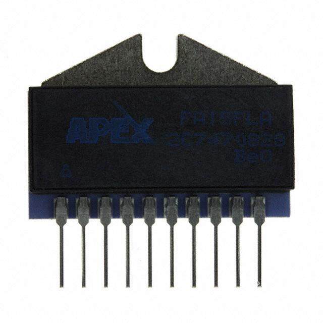
| 产品图片 |
|
| rohs | 符合RoHS无铅 / 符合限制有害物质指令(RoHS)规范要求 |
| 产品系列 | 放大器 IC,运算放大器 - 运放,Microchip Technology MCP6004-I/SL- |
| 数据手册 | http://www.microchip.com/mymicrochip/filehandler.aspx?ddocname=en011705http://www.microchip.com/mymicrochip/filehandler.aspx?ddocname=en023833 |
| 产品型号 | MCP6004-I/SL |
| 产品目录页面 | |
| 产品种类 | 运算放大器 - 运放 |
| 供应商器件封装 | 14-SOIC |
| 共模抑制比—最小值 | 60 dB |
| 关闭 | No Shutdown |
| 其它名称 | MCP6004ISL |
| 包装 | 管件 |
| 压摆率 | 0.6 V/µs |
| 商标 | Microchip Technology |
| 增益带宽生成 | 1 MHz |
| 增益带宽积 | 1MHz |
| 安装类型 | 表面贴装 |
| 安装风格 | SMD/SMT |
| 封装 | Tube |
| 封装/外壳 | 14-SOIC(0.154",3.90mm 宽) |
| 封装/箱体 | SOIC-14 |
| 工作温度 | -40°C ~ 85°C |
| 工作电源电压 | 1.8 V to 5.5 V |
| 工厂包装数量 | 57 |
| 技术 | CMOS |
| 放大器类型 | 通用 |
| 最大工作温度 | + 85 C |
| 最小工作温度 | - 40 C |
| 标准包装 | 57 |
| 电压-电源,单/双 (±) | 1.8 V ~ 6 V |
| 电压-输入失调 | 4.5mV |
| 电流-电源 | 100µA |
| 电流-输入偏置 | 1pA |
| 电流-输出/通道 | 23mA |
| 电源电流 | 0.1 mA |
| 电路数 | 4 |
| 转换速度 | 0.6 V/us |
| 输入偏压电流—最大 | 1 pA |
| 输入参考电压噪声 | 28 nV |
| 输入补偿电压 | 4.5 mV |
| 输出电流 | 23 mA |
| 输出类型 | 满摆幅 |
| 通道数量 | 4 Channel |


- 商务部:美国ITC正式对集成电路等产品启动337调查
- 曝三星4nm工艺存在良率问题 高通将骁龙8 Gen1或转产台积电
- 太阳诱电将投资9.5亿元在常州建新厂生产MLCC 预计2023年完工
- 英特尔发布欧洲新工厂建设计划 深化IDM 2.0 战略
- 台积电先进制程称霸业界 有大客户加持明年业绩稳了
- 达到5530亿美元!SIA预计今年全球半导体销售额将创下新高
- 英特尔拟将自动驾驶子公司Mobileye上市 估值或超500亿美元
- 三星加码芯片和SET,合并消费电子和移动部门,撤换高东真等 CEO
- 三星电子宣布重大人事变动 还合并消费电子和移动部门
- 海关总署:前11个月进口集成电路产品价值2.52万亿元 增长14.8%


PDF Datasheet 数据手册内容提取
MCP6001/2/4 1 MHz, Low-Power Op Amp Features Description • Available in SC-70-5 and SOT-23-5 packages The Microchip Technology Inc. MCP6001/2/4 family of (cid:127) Gain Bandwidth Product: 1MHz (typ.) operational amplifiers (op amps) is specifically designed for general-purpose applications. This family (cid:127) Rail-to-Rail Input/Output has a 1MHz Gain Bandwidth Product (GBWP) and (cid:127) Supply Voltage: 1.8V to 5.5V 90° phase margin (typ.). It also maintains 45° phase (cid:127) Supply Current: I = 100µA (typ.) Q margin (typ.) with a 500pF capacitive load. This family (cid:127) Phase Margin: 90° (typ.) operates from a single supply voltage as low as 1.8V, (cid:127) Temperature Range: while drawing 100µA (typ.) quiescent current. - Industrial: -40°C to +85°C Additionally, the MCP6001/2/4 supports rail-to-rail input and output swing, with a common mode input - Extended: -40°C to +125°C voltage range of V +300mV to V –300mV. This DD SS (cid:127) Available in Single, Dual and Quad Packages family of op amps is designed with Microchip’s advanced CMOS process. Applications The MCP6001/2/4 family is available in the industrial (cid:127) Automotive and extended temperature ranges, with a power supply (cid:127) Portable Equipment range of 1.8V to 5.5V. (cid:127) Photodiode Amplifier Package Types (cid:127) Analog Filters (cid:127) Notebooks and PDAs MCP6001 MCP6002 (cid:127) Battery-Powered Systems SC-70-5, SOT-23-5 PDIP, SOIC, MSOP Available Tools VVOOUUTT 11 55 VVDDDD VOUTA 1 8 VDD SPICE Macro Models (at www.microchip.com) VVSSSS 22 ++ -- VINA– 2 - + 7 VOUTB FilterLab® Software (at www.microchip.com) VIN+ 33 44 VIN– VINA+ 3 + - 6 VINB– VSS 4 5 VINB+ Typical Application MCP6001R V DD SOT-23-5 MCP6004 VIN + VOUT 1 5 VSS PDIP, SOIC, TSSOP MCP6001 VOUT VDD 2 + - VOUTA 1 14VOUTD – VIN+ 3 4 VIN– VINA– 2 - + + - 13VIND– VSS VINA+ 3 12VIND+ VDD 4 11VSS R MCP6001U VINB+ 5 10VINC+ 1 R2 SOT-23-5 VINB– 6 - + + - 9 VINC– R Gain = 1+----1-- VIN+ 1 5 VDD VOUTB 7 8 VOUTC R + VREF 2 VSS 2 - Non-Inverting Amplifier VIN– 3 4 VOUT 2004 Microchip Technology Inc. DS21733E-page 1
MCP6001/2/4 1.0 ELECTRICAL † Notice: Stresses above those listed under “Maximum CHARACTERISTICS Ratings” may cause permanent damage to the device. This is a stress rating only and functional operation of the device at those or any other conditions above those Absolute Maximum Ratings † indicated in the operational listings of this specification V – V ........................................................................7.0V is not implied. Exposure to maximum rating conditions DD SS for extended periods may affect device reliability. All Inputs and Outputs ...................V –0.3V to V +0.3V SS DD Difference Input Voltage ......................................|V – V | DD SS Output Short-Circuit Current .................................continuous Current at Input Pins ....................................................±2mA Current at Output and Supply Pins ............................±30mA Storage Temperature.....................................-65°C to +150°C Maximum Junction Temperature (T )..........................+150°C J ESD Protection On All Pins (HBM;MM)...............≥ 4kV; 200V DC ELECTRICAL SPECIFICATIONS Electrical Characteristics: Unless otherwise indicated, T = +25°C, V = +1.8V to +5.5V, V = GND, V = V /2, A DD SS CM DD R = 10kΩ to V /2 and V ≈V /2. L DD OUT DD Parameters Sym Min Typ Max Units Conditions Input Offset Input Offset Voltage V -4.5 — +4.5 mV V = V (Note1) OS CM SS Input Offset Drift with Temperature ∆V /∆T — ±2.0 — µV/°C T = -40°C to +125°C, OS A A V = V CM SS Power Supply Rejection Ratio PSRR — 86 — dB V = V CM SS Input Bias Current and Impedance Input Bias Current: I — ±1.0 — pA B Industrial Temperature I — 19 — pA T = +85°C B A Extended Temperature I — 1100 — pA T = +125°C B A Input Offset Current I — ±1.0 — pA OS Common Mode Input Impedance Z — 1013||6 — Ω||pF CM Differential Input Impedance Z — 1013||3 — Ω||pF DIFF Common Mode Common Mode Input Range V V − 0.3 — V + 0.3 V CMR SS DD Common Mode Rejection Ratio CMRR 60 76 — dB V = -0.3V to 5.3V, CM V = 5V DD Open-Loop Gain DC Open-Loop Gain (Large Signal) A 88 112 — dB V = 0.3V to V – 0.3V, OL OUT DD V =V CM SS Output Maximum Output Voltage Swing V , V V + 25 — V – 25 mV V = 5.5V OL OH SS DD DD Output Short-Circuit Current I — ±6 — mA V = 1.8V SC DD — ±23 — mA V = 5.5V DD Power Supply Supply Voltage V 1.8 — 5.5 V DD Quiescent Current per Amplifier I 50 100 170 µA I = 0, V = 5.5V, V = 5V Q O DD CM Note 1: MCP6001/2/4 parts with date codes prior to December 2004 (week code 49) were tested to ±7mV minimum/ maximum limits. DS21733E-page 2 2004 Microchip Technology Inc.
MCP6001/2/4 AC ELECTRICAL SPECIFICATIONS Electrical Characteristics: Unless otherwise indicated, T = +25°C, V = +1.8 to 5.5V, V = GND, V = V /2, A DD SS CM DD V ≈V /2, R = 10kΩ to V /2 and C = 60pF. OUT DD L DD L Parameters Sym Min Typ Max Units Conditions AC Response Gain Bandwidth Product GBWP — 1.0 — MHz Phase Margin PM — 90 — ° G = +1 Slew Rate SR — 0.6 — V/µs Noise Input Noise Voltage E — 6.1 — µVp-p f = 0.1Hz to 10Hz ni Input Noise Voltage Density e — 28 — nV/√Hz f = 1kHz ni Input Noise Current Density i — 0.6 — fA/√Hz f = 1kHz ni TEMPERATURE SPECIFICATIONS Electrical Characteristics: Unless otherwise indicated, V = +1.8V to +5.5V and V = GND. DD SS Parameters Sym Min Typ Max Units Conditions Temperature Ranges Industrial Temperature Range T -40 — +85 °C A Extended Temperature Range T -40 — +125 °C A Operating Temperature Range T -40 — +125 °C Note A Storage Temperature Range T -65 — +150 °C A Thermal Package Resistances Thermal Resistance, 5L-SC70 θ — 331 — °C/W JA Thermal Resistance, 5L-SOT-23 θ — 256 — °C/W JA Thermal Resistance, 8L-PDIP θ — 85 — °C/W JA Thermal Resistance, 8L-SOIC (150mil) θ — 163 — °C/W JA Thermal Resistance, 8L-MSOP θ — 206 — °C/W JA Thermal Resistance, 14L-PDIP θ — 70 — °C/W JA Thermal Resistance, 14L-SOIC θ — 120 — °C/W JA Thermal Resistance, 14L-TSSOP θ — 100 — °C/W JA Note: The industrial temperature devices operate over this extended temperature range, but with reduced performance. In any case, the internal Junction Temperature (T ) must not exceed the Absolute Maximum J specification of +150°C. 2004 Microchip Technology Inc. DS21733E-page 3
MCP6001/2/4 2.0 TYPICAL PERFORMANCE CURVES Note: The graphs and tables provided following this note are a statistical summary based on a limited number of samples and are provided for informational purposes only. The performance characteristics listed herein are not tested or guaranteed. In some graphs or tables, the data presented may be outside the specified operating range (e.g., outside specified power supply range) and therefore outside the warranted range. Note: Unless otherwise indicated, T = +25°C, V = +1.8V to +5.5V, V = GND, V = V /2, V ≈V /2, A DD SS CM DD OUT DD R = 10kΩ to V /2 and C = 60pF. L DD L 20% 100 es 18% 64,695 Samples of Occurrenc 11110246%%%% VCM = VSS CMRR (dB) 899505 PSRR (VCM = VSS) age 68%% RR, 80 cent 4% PS 75 CMRR (VCM = -0.3V to +5.3V) er 2% P 0% 70 5 -4 -3 -2 -1 0 1 2 3 4 5 -50 -25 0 25 50 75 100 125 Input Offset Voltage (mV) Ambient Temperature (°C) FIGURE 2-1: Input Offset Voltage. FIGURE 2-4: CMRR, PSRR vs. Ambient Temperature. 100 120 0 V = V 90 CM SS 100 -30 RR (dB) 7800 PSRR– Gain (dB) 6800 Phase --9600 Phase (°) PSRR, CM 456000 CMRRPSRR+ pen-Loop 2400 Gain --115200 pen-Loop 30 O 0 -180 O V = V CM SS 20 -20 -210 1.E1+001 1.E10+002 1.E1+k03 1.1E0+k04 11.E0+00k5 10..E1- 11.E 11.0E 110.E0 11.kE 110.Ek 110.0Ek11.ME 110.EM Frequency (Hz) 01 +00 +01F+r0e2qu+e0n3cy+ (0H4z)+05 +06 +07 FIGURE 2-2: PSRR, CMRR vs. FIGURE 2-5: Open-Loop Gain, Phase vs. Frequency. Frequency. Percentage of Occurrences 1112468024%%%%%%% 1VVT2ADC 3DM= 0 = =+ S 58Va.5D5m°DVCples Percentage of Occurrences 1122334455050505050505%%%%%%%%%%%% 6VVT0ADC 5DM= = S=+ a51Vm.2D55DpV°lCes 0% 0 0 0 0 0 0 0 0 0 0 0 0 3 6 9 12 15 18 21 24 27 30 15 30 45 60 75 90 105 120 135 150 Input Bias Current (pA) Input Bias Current (pA) FIGURE 2-3: Input Bias Current at +85°C. FIGURE 2-6: Input Bias Current at +125°C. DS21733E-page 4 2004 Microchip Technology Inc.
MCP6001/2/4 Note: Unless otherwise indicated, T = +25°C, V = +1.8V to +5.5V, V = GND, V = V /2, V ≈V /2, A DD SS CM DD OUT DD R = 10kΩ to V /2 and C = 60pF. L DD L nsity 1,000 nces 1168%% 1T2A 2=5 -S40a°mCp tloe s+125°C e De urre 1124%% VCM = VSS VoltagV/Hz)(cid:151) 100 of Occ 180%% e n e s( g 6% Noi nta 4% Input Perce 02%% 10 2 0 8 6 4 2 0 2 4 6 8 0 2 1.0E.1-01 1.E1+0 1.1E0+0 11.E0+00 1.1Ek+0 11.E0+k0 11.E00+k0 -1 -1 - - - - 1 1 0 F1reque2ncy (Hz3) 4 5 Input Offset Voltage Drift (µV/°C) FIGURE 2-7: Input Noise Voltage Density FIGURE 2-10: Input Offset Voltage Drift. vs. Frequency. 0 200 µV) -100 VDD = 1.8V µV) 150 ge ( -200 ge ( 100 olta -300 olta 50 VDD = 5.5V Offset V --540000 TTAA == +-4205°°CC Offset V -500 VDD = 1.8V Input --760000 TTAA == ++8152°5C°C Input --115000 VCM = VSS -200 4 2 0 2 4 6 8 0 2 4 6 8 0 2 0. 0. 0. 0. 0. 0. 0. 1. 1. 1. 1. 1. 2. 2. 0.0 0.5 1.0 1.5 2.0 2.5 3.0 3.5 4.0 4.5 5.0 5.5 - - Common Mode Input Voltage (V) Output Voltage (V) FIGURE 2-8: Input Offset Voltage vs. FIGURE 2-11: Input Offset Voltage vs. Common Mode Input Voltage at V = 1.8V. Output Voltage. DD 0 30 V = 5.5V put Offset Voltage (µV) ------654321000000000000 DD TTTTAAA = === + ++-142820555°°°C°CCC Short Circuit CurrentMagnitude (mA) 112250505 TTTAT AA=A == =+ ++1-28245550°°°°CCCC n A I -700 0 5 0 5 0 5 0 5 0 5 0 5 0 5 0 0. 0. 0. 1. 1. 2. 2. 3. 3. 4. 4. 5. 5. 6. 0.0 0.5 1.0 1.5 2.0 2.5 3.0 3.5 4.0 4.5 5.0 5.5 - Common Mode Input Voltage (V) Power Supply Voltage (V) FIGURE 2-9: Input Offset Voltage vs. FIGURE 2-12: Output Short-Circuit Current Common Mode Input Voltage at V = 5.5V. vs. Power Supply Voltage. DD 2004 Microchip Technology Inc. DS21733E-page 5
MCP6001/2/4 Note: Unless otherwise indicated, T = +25°C, V = +1.8V to +5.5V, V = GND, V = V /2, V ≈V /2, A DD SS CM DD OUT DD R = 10kΩ to V /2 and C = 60pF. L DD L 1.0 0.08 G = +1 V/V 0.9 Falling Edge, VDD = 5.5V v) 0.06 0.8 Falling Edge, VDD = 1.8V di µs) 0.7 mV/ 0.04 ate (V/ 00..56 e (20 0.02 Slew R 000...234 RisinRgis Eindgg Ee,d VgDeD, V= D1D. 8=V 5.5V ut Voltag-00..0020 0.1 utp-0.04 0.0 O-0.06 -50 -25 0 25 50 75 100 125 -0.008.E+00 1.E-06 2.E-06 3.E-06 4.E-06 5.E-06 6.E-06 7.E-06 8.E-06 9.E-06 1.E-05 Ambient Temperature (°C) Time (1 µs/div) FIGURE 2-13: Slew Rate vs. Ambient FIGURE 2-16: Small-Signal, Non-Inverting Temperature. Pulse Response. 1,000 5.0 G = +1 V/V m 4.5 oo 4.0 VDD = 5.0V age HeadrmV) 100 VDD – VOHVOL – VSS oltage (V) 233...505 Volt( 10 ut V 2.0 utput Outp 11..05 O 1 0.5 1.1E0-µ05 11.E0-00µ4 1.1Em-03 11.E0-m02 0.0 0.E+00 1.E-05 2.E-05 3.E-05 4.E-05 5.E-05 6.E-05 7.E-05 8.E-05 9.E-05 1.E-04 Output Current Magnitude (A) Time (10 µs/div) FIGURE 2-14: Output Voltage Headroom FIGURE 2-17: Large-Signal, Non-Inverting vs. Output Current Magnitude. Pulse Response. 10 180 V = V - 0.5V )P-P 160 CM DD ut Voltage Swing (V 1 VVDDDD == 51..58VV Quiescent Currentper amplifier (µA) 111468024000000 TTTA AA= == + ++1282555°°°CCC utp 20 TA = -40°C O 0 0.1 1.E1+k03 1.1E0+k04 11.E00+k05 1.E1M+06 0.0 0.5 1.0 1.5 2.0 2.5 3.0 3.5 4.0 4.5 5.0 5.5 Frequency (Hz) Power Supply Voltage (V) FIGURE 2-15: Output Voltage Swing vs. FIGURE 2-18: Quiescent Current vs. Frequency. Power Supply Voltage. DS21733E-page 6 2004 Microchip Technology Inc.
MCP6001/2/4 3.0 PIN DESCRIPTIONS Descriptions of the pins are listed in Table3-1. TABLE 3-1: PIN FUNCTION TABLE MCP6001 MCP6001R MCP6001U MCP6002 MCP6004 Symbol Description 1 1 4 1 1 V , V Analog Output (op amp A) OUT OUTA 4 4 3 2 2 V –, V – Inverting Input (op amp A) IN INA 3 3 1 3 3 V +, V + Non-inverting Input (op amp A) IN INA 5 2 5 8 4 V Positive Power Supply DD — — — 5 5 V + Non-inverting Input (op amp B) INB — — — 6 6 V – Inverting Input (op amp B) INB — — — 7 7 V Analog Output (op amp B) OUTB — — — — 8 V Analog Output (op amp C) OUTC — — — — 9 V – Inverting Input (op amp C) INC — — — — 10 V + Non-inverting Input (op amp C) INC 2 5 2 4 11 V Negative Power Supply SS — — — — 12 V + Non-inverting Input (op amp D) IND — — — — 13 V – Inverting Input (op amp D) IND — — — — 14 V Analog Output (op amp D) OUTD 3.1 Analog Outputs 3.3 Power Supply (V and V ) SS DD The output pins are low-impedance voltage sources. The positive power supply (V ) is 1.8V to 5.5V higher DD than the negative power supply (V ). For normal SS 3.2 Analog Inputs operation, the other pins are at voltages between VSS and V . DD The non-inverting and inverting inputs are high- Typically, these parts are used in a single (positive) impedance CMOS inputs with low bias currents. supply configuration. In this case, V is connected to SS ground and V is connected to the supply. V will DD DD need a local bypass capacitor (typically 0.01µF to 0.1µF) within 2mm of the V pin. These parts can DD share a bulk capacitor with analog parts (typically 2.2µF to 10µF) within 100mm of the V pin. DD 2004 Microchip Technology Inc. DS21733E-page 7
MCP6001/2/4 4.0 APPLICATION INFORMATION The MCP6001/2/4 family of op amps is manufactured – using Microchip’s state-of-the-art CMOS process and is specifically designed for low-cost, low-power and RIN MCP600X VOUT general-purpose applications. The low supply voltage, VIN + low quiescent current and wide bandwidth makes the MCP6001/2/4 ideal for battery-powered applications. This device has high phase margin, which makes it (Maximum expected V )–V R ≥-------------------------------------------------------I--N----------------D---D--- stable for larger capacitive load applications. IN 2 mA V –(Minimum expected V ) 4.1 Rail-to-Rail Input R ≥----S---S--------------------------------------------------------------I--N----- IN 2 mA The MCP6001/2/4 op amps are designed to prevent phase reversal when the input pins exceed the supply FIGURE 4-2: Input Current Limiting voltages. Figure4-1 shows the input voltage exceeding Resistor (RIN). the supply voltage without any phase reversal. 4.2 Rail-to-Rail Output 6 The output voltage range of the MCP6001/2/4 op amps V V = 5.0V V) 5 IN GD =D +2 V/V is VDD–25mV (min.) and VSS + 25mV (max.) when ges ( 4 VOUT RRLef=er1 t0o kFΩig uisre c2o-n1n4e fcotre md otore VinDfoDr/m2 aatniodn .VDD = 5.5V. a olt 3 V put 2 4.3 Capacitive Loads ut ut, O 1 Dlermivsin fgo rl avrogltea gcaep faeceidtibvaec lko aodps a cmapns c. aAuss eth set alobaildit yc approabc-- Inp 0 itance increases, the feedback loop’s phase margin -1 decreases and the closed-loop bandwidth is reduced. 0.E+00 1.E-05 2.E-05 3.E-05 4.E-05 5.E-05 6.E-05 7.E-05 8.E-05 9.E-05 1.E-04 Time (10 µs/div) This produces gain peaking in the frequency response, with overshoot and ringing in the step response. While FIGURE 4-1: The MCP6001/2/4 Show No a unity-gain buffer (G = +1) is the most sensitive to Phase Reversal. capacitive loads, all gains show the same general behavior. The input stage of the MCP6001/2/4 op amps use two differential input stages in parallel. One operates at a When driving large capacitive loads with these op low common mode input voltage (V ), while the other amps (e.g., > 100pF when G = +1), a small series CM operates at a high V . With this topology, the device resistor at the output (R in Figure4-3) improves the CM ISO operates with a V up to 300mV above V and feedback loop’s phase margin (stability) by making the CM DD 300mV below V . The input offset voltage is output load resistive at higher frequencies. The band- SS measured at V =V –300mV and V +300mV width will be generally lower than the bandwidth with no CM SS DD to ensure proper operation. capacitance load. Input voltages that exceed the input voltage range (V –0.3V to V +0.3V at 25°C) can cause SS DD excessive current to flow into or out of the input pins, – R while current beyond ±2mA can cause reliability ISO problems. Applications that exceed this rating must be MCP600X VOUT externally limited with a resistor, as shown in Figure4-2. V + IN C L FIGURE 4-3: Output resistor, R ISO stabilizes large capacitive loads. DS21733E-page 8 2004 Microchip Technology Inc.
MCP6001/2/4 Figure4-4 gives recommended R values for 4.5 PCB Surface Leakage ISO different capacitive loads and gains. The x-axis is the normalized load capacitance (C /G ), where G is the In applications where low input bias current is critical, L N N circuit's noise gain. For non-inverting gains, G and the Printed Circuit Board (PCB) surface leakage effects N Signal Gain are equal. For inverting gains, G is need to be considered. Surface leakage is caused by N 1+|Signal Gain| (e.g., -1 V/V gives G = +2 V/V). humidity, dust or other contamination on the board. N Under low humidity conditions, a typical resistance between nearby traces is 1012Ω. A 5V difference would 1000 cause 5pA of current to flow; which is greater than the V = 5.0V DD MCP6001/2/4 family’s bias current at 25°C (1pA, typ.). )(cid:58) RL = 100 k(cid:58) (O The easiest way to reduce surface leakage is to use a S d RI guard ring around sensitive pins (or traces). The guard de 100 ring is biased at the same voltage as the sensitive pin. en GN = 1 An example of this type of layout is shown in m m GN (cid:116) 2 Figure4-5. o c e R V - V + 10 IN IN VSS 11.E0-p11 11.E00-1p0 1.E1n-09 111.E00-nn08 Normalized Load Capacitance; C/G (F) L N FIGURE 4-4: Recommended R values ISO for Capacitive Loads. After selecting R for your circuit, double-check the ISO resulting frequency response peaking and step response overshoot. Modify R ’s value until the ISO Guard Ring response is reasonable. Bench evaluation and simula- tions with the MCP6001/2/4 SPICE macro model are FIGURE 4-5: Example Guard Ring Layout very helpful. for Inverting Gain. 1. Non-inverting Gain and Unity-Gain Buffer: 4.4 Supply Bypass a. Connect the non-inverting pin (V +) to the IN With this family of operational amplifiers, the power input with a wire that does not touch the supply pin (VDD for single-supply) should have a local PCB surface. bypass capacitor (i.e., 0.01µF to 0.1µF) within 2mm b. Connect the guard ring to the inverting input for good high-frequency performance. It also needs a pin (V –). This biases the guard ring to the IN bulk capacitor (i.e., 1µF or larger) within 100mm to common mode input voltage. provide large, slow currents. This bulk capacitor can be 2. Inverting Gain and Transimpedance Gain shared with other analog parts. Amplifiers (convert current to voltage, such as photo detectors): a. Connect the guard ring to the non-inverting input pin (V +). This biases the guard ring IN to the same reference voltage as the op amp (e.g., V /2 or ground). DD b. Connect the inverting pin (V –) to the input IN with a wire that does not touch the PCB surface. 2004 Microchip Technology Inc. DS21733E-page 9
MCP6001/2/4 4.6 Application Circuits 100pF 4.6.1 UNITY-GAIN BUFFER The rail-to-rail input and output capability of the V 14.3kΩ 53.6kΩ MCP6001/2/4 op amp is ideal for unity-gain buffer IN + applications. The low quiescent current and wide bandwidth makes the device suitable for a buffer MCP6002 configuration in an instrumentation amplifier circuit, as 33pF – VOUT shown in Figure4-6. FIGURE 4-7: Active Second-Order – 1/2 R2 R1 Low- Pass Filter. MCP6002 VIN1 + 4.6.3 PEAK DETECTOR – The MCP6001/2/4 op amp has a high input impedance, MCP6001 VOUT rail-to-rail input/output and low input bias current, which + makes this device suitable for peak detector applica- – 1/2 R2 tions. Figure4-8 shows a peak detector circuit with MCP6002 clear and sample switches. The peak-detection cycle VIN2 + R = 20kΩ uses a clock (CLK), as shown in Figure4-8. 1 R1 R = 10kΩ At the rising edge of CLK, Sample Switch closes to 2 VREF begin sampling. The peak voltage stored on C1 is sam- pled to C for a sample time defined by t . At the R 2 SAMP V = (V –V )•----1--+V end of the sample time (falling edge of Sample Signal), OUT IN2 IN1 R2 REF Clear Signal goes high and closes the Clear Switch. When the Clear Switch closes, C discharges through 1 FIGURE 4-6: Instrumentation Amplifier R for a time defined by t . At the end of the clear 1 CLEAR with Unity-Gain Buffer Inputs. time (falling edge of Clear Signal), op amp A begins to store the peak value of V on C for a time defined by IN 1 4.6.2 ACTIVE LOW-PASS FILTER t . DETECT The MCP6001/2/4 op amp’s low input bias current In order to define t and t , it is necessary to SAMP CLEAR makes it possible for the designer to use larger resis- determine the capacitor charging and discharging tors and smaller capacitors for active low-pass filter period. The capacitor charging time is limited by the τ applications. However, as the resistance increases, the amplifier source current, while the discharging time ( ) τ noise generated also increases. Parasitic capacitances is defined using R ( = R C ). t is the time that 1 1 1 DETECT and the large value resistors could also modify the fre- the input signal is sampled on C and is dependent on 1 quency response. These trade-offs need to be the input voltage change frequency. considered when selecting circuit elements. The op amp output current limit, and the size of the Usually, the op amp bandwidth is 100X the filter cutoff storage capacitors (both C and C ), could create slew- 1 2 frequency (or higher) for good performance. It is possi- ing limitations as the input voltage (V ) increases. IN ble to have the op amp bandwidth 10X higher than the Current through a capacitor is dependent on the size of cutoff frequency, thus having a design that is more the capacitor and the rate of voltage change. From this sensitive to component tolerances. relationship, the rate of voltage change or the slew rate can be determined. For example, with an op amp short- Figure4-7 shows a second-order Butterworth filter with circuit current of I = 25mA and a load capacitor of 100kHz cutoff frequency and a gain of +1V/V; the op SC C =0.1µF, then: amp bandwidth is only 10X higher than the cutoff 1 frequency. The component values were selected using Microchip’s FilterLab® software. EQUATION 4-1: dV I = C --------C---1-- SC 1 dt dV I --------C---1-- = ---S---C-- dt C 1 25mA = --------------- 0.1µF dV --------C---1-- = 250mV⁄µs dt DS21733E-page 10 2004 Microchip Technology Inc.
MCP6001/2/4 This voltage rate of change is less than the MCP6001/2/4 slew rate of 0.6V/µs. When the input voltage swings below the voltage across C , D becomes reverse- 1 1 biased. This opens the feedback loop and rails the amplifier. When the input voltage increases, the amplifier recovers at its slew rate. Based on the rate of voltage change shown in the above equation, it takes an extended period of time to charge a 0.1µF capacitor. The capacitors need to be selected so that the circuit is not limited by the amplifier slew rate. Therefore, the capaci- tors should be less than 40µF and a stabilizing resistor (R ) needs to be properly selected. (Refer to ISO Section4.3 “Capacitive Loads”). V IN +1/2 D1 RISO VC1 MCP6002 +1/2 RISO VC2 – Op Amp A C1 R1 M–CP6002 M+CP6001 VOUT C Op Amp B 2 – Op Amp C Sample Switch Clear Switch t SAMP Sample Signal t CLEAR Clear Signal t DETECT CLK FIGURE 4-8: Peak Detector with Clear and Sample CMOS Analog Switches. 2004 Microchip Technology Inc. DS21733E-page 11
MCP6001/2/4 5.0 DESIGN TOOLS Microchip provides the basic design tools needed for the MCP6001/2/4 family of op amps. 5.1 SPICE Macro Model The latest SPICE macro model for the MCP6001/2/4 op amps is available on our web site at www.microchip.com. This model is intended to be an initial design tool that works well in the op amp’s linear region of operation at room temperature. See the model file for information on its capabilities. Bench testing is a very important part of any design and cannot be replaced with simulations. Also, simulation results using this macro model need to be validated by comparing them to the data sheet specifications and characteristic curves. 5.2 FilterLab® Software Microchip’s FilterLab® software is an innovative software tool that simplifies analog active filter (using op amps) design. Available at no cost from our web site at www.microchip.com, the FilterLab design tool provides full schematic diagrams of the filter circuit with component values. It also outputs the filter circuit in SPICE format, which can be used with the macro model to simulate actual filter performance. DS21733E-page 12 2004 Microchip Technology Inc.
MCP6001/2/4 6.0 PACKAGING INFORMATION 6.1 Package Marking Information 5-Lead SC-70 (MCP6001) Example: (I-Temp) XXN (Front) Device I-Temp E-Temp AN7 (Front) YWW (Back) Code Code 432 (Back) MCP6001 ANN CDN Note: Applies to 5-Lead SC-70. 5-Lead SOT-23 (MCP6001/1R/1U) Example: (E-Temp) 5 4 I-Temp E-Temp 5 4 Device Code Code XXNN MCP6001 AANN CDNN CD25 MCP6001R ADNN CENN 1 2 3 MCP6001U AFNN CFNN 1 2 3 Note: Applies to 5-Lead SOT-23. 8-Lead PDIP (300 mil) Example: XXXXXXXX MCP6002 XXXXXNNN I/P256 YYWW 0432 8-Lead SOIC (150 mil) Example: XXXXXXXX MCP6002 XXXXYYWW I/SN0432 NNN 256 8-Lead MSOP Example: XXXXXX 6002I YWWNNN 432256 Legend: XX...X Customer specific information* YY Year code (last 2 digits of calendar year) WW Week code (week of January 1 is week ‘01’) NNN Alphanumeric traceability code Note: In the event the full Microchip part number cannot be marked on one line, it will be carried over to the next line thus limiting the number of available characters for customer specific information. * Standard marking consists of Microchip part number, year code, week code, traceability code (facility code, mask rev#, and assembly code). For marking beyond this, certain price adders apply. Please check with your Microchip Sales Office. 2004 Microchip Technology Inc. DS21733E-page 13
MCP6001/2/4 Package Marking Information (Continued) 14-Lead PDIP (300 mil) (MCP6004) Example: XXXXXXXXXXXXXX MCP6004-I/P XXXXXXXXXXXXXX YYWWNNN 0432256 14-Lead SOIC (150 mil) (MCP6004) Example: XXXXXXXXXX MCP6004ISL XXXXXXXXXX YYWWNNN 0432256 14-Lead TSSOP (MCP6004) Example: XXXXXX 6004ST YYWW 0432 NNN 256 DS21733E-page 14 2004 Microchip Technology Inc.
MCP6001/2/4 5-Lead Plastic Package (SC-70) E E1 D p B n 1 Q1 A2 A c A1 L Units INCHES MILLIMETERS* Dimension Limits MIN NOM MAX MIN NOM MAX Number of Pins n 5 5 Pitch p .026 (BSC) 0.65 (BSC) Overall Height A .031 .043 0.80 1.10 Molded Package Thickness A2 .031 .039 0.80 1.00 Standoff A1 .000 .004 0.00 0.10 Overall Width E .071 .094 1.80 2.40 Molded Package Width E1 .045 .053 1.15 1.35 Overall Length D .071 .087 1.80 2.20 Foot Length L .004 .012 0.10 0.30 Top of Molded Pkg to Lead Shoulder Q1 .004 .016 0.10 0.40 Lead Thickness c .004 .007 0.10 0.18 Lead Width B .006 .012 0.15 0.30 *Controlling Parameter Notes: Dimensions D and E1 do not include mold flash or protrusions. Mold flash or protrusions shall not exceed .005" (0.127mm) per side. JEITA (EIAJ) Standard: SC-70 Drawing No. C04-061 2004 Microchip Technology Inc. DS21733E-page 15
MCP6001/2/4 5-Lead Plastic Small Outline Transistor (OT) (SOT23) E E1 p B p1 D n 1 α c A A2 φ A1 β L Units INCHES* MILLIMETERS Dimension Limits MIN NOM MAX MIN NOM MAX Number of Pins n 5 5 Pitch p .038 0.95 Outside lead pitch (basic) p1 .075 1.90 Overall Height A .035 .046 .057 0.90 1.18 1.45 Molded Package Thickness A2 .035 .043 .051 0.90 1.10 1.30 Standoff § A1 .000 .003 .006 0.00 0.08 0.15 Overall Width E .102 .110 .118 2.60 2.80 3.00 Molded Package Width E1 .059 .064 .069 1.50 1.63 1.75 Overall Length D .110 .116 .122 2.80 2.95 3.10 Foot Length L .014 .018 .022 0.35 0.45 0.55 Foot Angle φ 0 5 10 0 5 10 Lead Thickness c .004 .006 .008 0.09 0.15 0.20 Lead Width B .014 .017 .020 0.35 0.43 0.50 Mold Draft Angle Top α 0 5 10 0 5 10 Mold Draft Angle Bottom β 0 5 10 0 5 10 * Controlling Parameter § Significant Characteristic Notes: Dimensions D and E1 do not include mold flash or protrusions. Mold flash or protrusions shall not exceed .010” (0.254mm) per side. JEDEC Equivalent: MO-178 Drawing No. C04-091 DS21733E-page 16 2004 Microchip Technology Inc.
MCP6001/2/4 8-Lead Plastic Dual In-line (P) – 300 mil (PDIP) E1 D 2 n 1 α E A A2 L c A1 β B1 p eB B Units INCHES* MILLIMETERS Dimension Limits MIN NOM MAX MIN NOM MAX Number of Pins n 8 8 Pitch p .100 2.54 Top to Seating Plane A .140 .155 .170 3.56 3.94 4.32 Molded Package Thickness A2 .115 .130 .145 2.92 3.30 3.68 Base to Seating Plane A1 .015 0.38 Shoulder to Shoulder Width E .300 .313 .325 7.62 7.94 8.26 Molded Package Width E1 .240 .250 .260 6.10 6.35 6.60 Overall Length D .360 .373 .385 9.14 9.46 9.78 Tip to Seating Plane L .125 .130 .135 3.18 3.30 3.43 Lead Thickness c .008 .012 .015 0.20 0.29 0.38 Upper Lead Width B1 .045 .058 .070 1.14 1.46 1.78 Lower Lead Width B .014 .018 .022 0.36 0.46 0.56 Overall Row Spacing § eB .310 .370 .430 7.87 9.40 10.92 Mold Draft Angle Top α 5 10 15 5 10 15 Mold Draft Angle Bottom β 5 10 15 5 10 15 * Controlling Parameter § Significant Characteristic Notes: Dimensions D and E1 do not include mold flash or protrusions. Mold flash or protrusions shall not exceed .010” (0.254mm) per side. JEDEC Equivalent: MS-001 Drawing No. C04-018 2004 Microchip Technology Inc. DS21733E-page 17
MCP6001/2/4 8-Lead Plastic Small Outline (SN) – Narrow, 150 mil (SOIC) E E1 p D 2 B n 1 h α 45° c A A2 φ β L A1 Units INCHES* MILLIMETERS Dimension Limits MIN NOM MAX MIN NOM MAX Number of Pins n 8 8 Pitch p .050 1.27 Overall Height A .053 .061 .069 1.35 1.55 1.75 Molded Package Thickness A2 .052 .056 .061 1.32 1.42 1.55 Standoff § A1 .004 .007 .010 0.10 0.18 0.25 Overall Width E .228 .237 .244 5.79 6.02 6.20 Molded Package Width E1 .146 .154 .157 3.71 3.91 3.99 Overall Length D .189 .193 .197 4.80 4.90 5.00 Chamfer Distance h .010 .015 .020 0.25 0.38 0.51 Foot Length L .019 .025 .030 0.48 0.62 0.76 Foot Angle φ 0 4 8 0 4 8 Lead Thickness c .008 .009 .010 0.20 0.23 0.25 Lead Width B .013 .017 .020 0.33 0.42 0.51 Mold Draft Angle Top α 0 12 15 0 12 15 Mold Draft Angle Bottom β 0 12 15 0 12 15 * Controlling Parameter § Significant Characteristic Notes: Dimensions D and E1 do not include mold flash or protrusions. Mold flash or protrusions shall not exceed .010” (0.254mm) per side. JEDEC Equivalent: MS-012 Drawing No. C04-057 DS21733E-page 18 2004 Microchip Technology Inc.
MCP6001/2/4 8-Lead Plastic Micro Small Outline Package (MS) (MSOP) E E1 p D 2 B n 1 α A A2 c φ A1 (F) L β Units INCHES MILLIMETERS* Dimension Limits MIN NOM MAX MIN NOM MAX Number of Pins n 8 8 Pitch p .026 BSC 0.65 BSC Overall Height A - - .043 - - 1.10 Molded Package Thickness A2 .030 .033 .037 0.75 0.85 0.95 Standoff A1 .000 - .006 0.00 - 0.15 Overall Width E .193 TYP. 4.90 BSC Molded Package Width E1 .118 BSC 3.00 BSC Overall Length D .118 BSC 3.00 BSC Foot Length L .016 .024 .031 0.40 0.60 0.80 Footprint (Reference) F .037 REF 0.95 REF Foot Angle φ 0° - 8° 0° - 8° Lead Thickness c .003 .006 .009 0.08 - 0.23 Lead Width B .009 .012 .016 0.22 - 0.40 Mold Draft Angle Top α 5° - 15° 5° - 15° Mold Draft Angle Bottom β 5° - 15° 5° - 15° *Controlling Parameter Notes: Dimensions D and E1 do not include mold flash or protrusions. Mold flash or protrusions shall not exceed .010" (0.254mm) per side. JEDEC Equivalent: MO-187 Drawing No. C04-111 2004 Microchip Technology Inc. DS21733E-page 19
MCP6001/2/4 14-Lead Plastic Dual In-line (P) – 300 mil (PDIP) E1 D 2 n 1 α E A A2 c L A1 β B1 eB B p Units INCHES* MILLIMETERS Dimension Limits MIN NOM MAX MIN NOM MAX Number of Pins n 14 14 Pitch p .100 2.54 Top to Seating Plane A .140 .155 .170 3.56 3.94 4.32 Molded Package Thickness A2 .115 .130 .145 2.92 3.30 3.68 Base to Seating Plane A1 .015 0.38 Shoulder to Shoulder Width E .300 .313 .325 7.62 7.94 8.26 Molded Package Width E1 .240 .250 .260 6.10 6.35 6.60 Overall Length D .740 .750 .760 18.80 19.05 19.30 Tip to Seating Plane L .125 .130 .135 3.18 3.30 3.43 Lead Thickness c .008 .012 .015 0.20 0.29 0.38 Upper Lead Width B1 .045 .058 .070 1.14 1.46 1.78 Lower Lead Width B .014 .018 .022 0.36 0.46 0.56 Overall Row Spacing § eB .310 .370 .430 7.87 9.40 10.92 Mold Draft Angle Top α 5 10 15 5 10 15 Mold Draft Angle Bottom β 5 10 15 5 10 15 * Controlling Parameter § Significant Characteristic Notes: Dimensions D and E1 do not include mold flash or protrusions. Mold flash or protrusions shall not exceed .010” (0.254mm) per side. JEDEC Equivalent: MS-001 Drawing No. C04-005 DS21733E-page 20 2004 Microchip Technology Inc.
MCP6001/2/4 14-Lead Plastic Small Outline (SL) – Narrow, 150 mil (SOIC) E E1 p D 2 B n 1 α h 45° c A A2 φ A1 L β Units INCHES* MILLIMETERS Dimension Limits MIN NOM MAX MIN NOM MAX Number of Pins n 14 14 Pitch p .050 1.27 Overall Height A .053 .061 .069 1.35 1.55 1.75 Molded Package Thickness A2 .052 .056 .061 1.32 1.42 1.55 Standoff § A1 .004 .007 .010 0.10 0.18 0.25 Overall Width E .228 .236 .244 5.79 5.99 6.20 Molded Package Width E1 .150 .154 .157 3.81 3.90 3.99 Overall Length D .337 .342 .347 8.56 8.69 8.81 Chamfer Distance h .010 .015 .020 0.25 0.38 0.51 Foot Length L .016 .033 .050 0.41 0.84 1.27 Foot Angle φ 0 4 8 0 4 8 Lead Thickness c .008 .009 .010 0.20 0.23 0.25 Lead Width B .014 .017 .020 0.36 0.42 0.51 Mold Draft Angle Top α 0 12 15 0 12 15 Mold Draft Angle Bottom β 0 12 15 0 12 15 * Controlling Parameter § Significant Characteristic Notes: Dimensions D and E1 do not include mold flash or protrusions. Mold flash or protrusions shall not exceed .010” (0.254mm) per side. JEDEC Equivalent: MS-012 Drawing No. C04-065 2004 Microchip Technology Inc. DS21733E-page 21
MCP6001/2/4 14-Lead Plastic Thin Shrink Small Outline (ST) – 4.4 mm (TSSOP) E E1 p D 2 n 1 B α A c φ β A1 A2 L Units INCHES MILLIMETERS* Dimension Limits MIN NOM MAX MIN NOM MAX Number of Pins n 14 14 Pitch p .026 0.65 Overall Height A .043 1.10 Molded Package Thickness A2 .033 .035 .037 0.85 0.90 0.95 Standoff § A1 .002 .004 .006 0.05 0.10 0.15 Overall Width E .246 .251 .256 6.25 6.38 6.50 Molded Package Width E1 .169 .173 .177 4.30 4.40 4.50 Molded Package Length D .193 .197 .201 4.90 5.00 5.10 Foot Length L .020 .024 .028 0.50 0.60 0.70 Foot Angle φ 0 4 8 0 4 8 Lead Thickness c .004 .006 .008 0.09 0.15 0.20 Lead Width B1 .007 .010 .012 0.19 0.25 0.30 Mold Draft Angle Top α 0 5 10 0 5 10 Mold Draft Angle Bottom β 0 5 10 0 5 10 * Controlling Parameter § Significant Characteristic Notes: Dimensions D and E1 do not include mold flash or protrusions. Mold flash or protrusions shall not exceed .005” (0.127mm) per side. JEDEC Equivalent: MO-153 Drawing No. C04-087 DS21733E-page 22 2004 Microchip Technology Inc.
MCP6001/2/4 APPENDIX A: REVISION HISTORY Revision A (June 2002) Original data sheet release. Revision B (October 2002) Revision C (December 2002) Revision D (May 2003) Revision E (December 2004) The following is the list of modifications: 1. V specification reduced to ±4.5mV from OS ±7.0mV for parts starting with date code YYWW = 0449 2. Corrected package markings in Section6.0 “Packaging Information” 3. Added Appendix A: Revision History. 2004 Microchip Technology Inc. DS21733E-page 23
MCP6001/2/4 NOTES: DS21733E-page 24 2004 Microchip Technology Inc.
MCP6001/2/4 PRODUCT IDENTIFICATION SYSTEM To order or obtain information, e.g., on pricing or delivery, refer to the factory or the listed sales office. PART NO. X /XX Examples: a) MCP6001T-I/LT: Tape and Reel, Device Temperature Package Industrial Temperature, Range 5LD SC-70 package b) MCP6001T-I/OT: Tape and Reel, Industrial Temperature, Device: MCP6001T: Single Op Amp (Tape and Reel) (SC-70, SOT-23) 5LD SOT-23 package. MCP6001RT: Single Op Amp (Tape and Reel) (SOT-23) c) MCP6001RT-I/OT: Tape and Reel, MCP6001UT: Single Op Amp (Tape and Reel) (SOT-23) Industrial Temperature, MCP6002: Dual Op Amp 5LD SOT-23 package. MCP6002T: Dual Op Amp (Tape and Reel) d) MCP6001UT-E/OT: Tape and Reel, (SOIC, MSOP) Extended Temperature, MCP6004: Quad Op Amp MCP6004T: Quad Op Amp (Tape and Reel) 5LD SOT-23 package. (SOIC, MSOP) a) MCP6002-I/MS: Industrial Temperature, 8LD MSOP package. Temperature Range: I = -40°C to +85°C b) MCP6002-I/P: Industrial Temperature, E = -40°C to +125°C 8LD PDIP package. c) MCP6002-E/P: Extended Temperature, Package: LT = Plastic Package (SC-70), 5-lead (MCP6001 only) 8LD PDIP package. OT = Plastic Small Outline Transistor (SOT-23), 5-lead d) MCP6002-I/SN: Industrial Temperature, (MCP6001, MCP6001R, MCP6001U) 8LD SOIC package. MS = Plastic MSOP, 8-lead P = Plastic DIP (300 mil Body), 8-lead, 14-lead e) MCP6002T-I/MS: Tape and Reel, SN = Plastic SOIC, (150 mil Body), 8-lead Industrial Temperature, SL = Plastic SOIC (150 mil Body), 14-lead 8LD MSOP package. ST = Plastic TSSOP (4.4mm Body), 14-lead a) MCP6004-I/P: Industrial Temperature, 14LD PDIP package. b) MCP6004-I/SL: Industrial Temperature,, 14LD SOIC package. c) MCP6004-E/SL: Extended Temperature,, 14LD SOIC package. d) MCP6004-I/ST: Industrial Temperature, 14LD TSSOP package. e) MCP6004T-I/SL: Tape and Reel, Industrial Temperature, 14LD SOIC package. f) MCP6004T-I/ST: Tape and Reel, Industrial Temperature, 14LD TSSOP package. Sales and Support Data Sheets Products supported by a preliminary Data Sheet may have an errata sheet describing minor operational differences and recommended workarounds. To determine if an errata sheet exists for a particular device, please contact one of the following: 1. Your local Microchip sales office 2. The Microchip Worldwide Site (www.microchip.com) Please specify which device, revision of silicon and Data Sheet (include Literature #) you are using. Customer Notification System Register on our web site (www.microchip.com) to receive the most current information on our products. 2004 Microchip Technology Inc. DS21733E-page 25
MCP6001/2/4 NOTES: DS21733E-page 26 2004 Microchip Technology Inc.
Note the following details of the code protection feature on Microchip devices: (cid:127) Microchip products meet the specification contained in their particular Microchip Data Sheet. (cid:127) Microchip believes that its family of products is one of the most secure families of its kind on the market today, when used in the intended manner and under normal conditions. (cid:127) There are dishonest and possibly illegal methods used to breach the code protection feature. All of these methods, to our knowledge, require using the Microchip products in a manner outside the operating specifications contained in Microchip’s Data Sheets. Most likely, the person doing so is engaged in theft of intellectual property. (cid:127) Microchip is willing to work with the customer who is concerned about the integrity of their code. (cid:127) Neither Microchip nor any other semiconductor manufacturer can guarantee the security of their code. Code protection does not mean that we are guaranteeing the product as “unbreakable.” Code protection is constantly evolving. We at Microchip are committed to continuously improving the code protection features of our products. Attempts to break Microchip’s code protection feature may be a violation of the Digital Millennium Copyright Act. If such acts allow unauthorized access to your software or other copyrighted work, you may have a right to sue for relief under that Act. Information contained in this publication regarding device Trademarks applications and the like is provided only for your convenience The Microchip name and logo, the Microchip logo, Accuron, and may be superseded by updates. It is your responsibility to dsPIC, KEELOQ, microID, MPLAB, PIC, PICmicro, ensure that your application meets with your specifications. PICSTART, PROMATE, PowerSmart, rfPIC, and MICROCHIP MAKES NO REPRESENTATIONS OR WAR- SmartShunt are registered trademarks of Microchip RANTIES OF ANY KIND WHETHER EXPRESS OR IMPLIED, Technology Incorporated in the U.S.A. and other countries. WRITTEN OR ORAL, STATUTORY OR OTHERWISE, RELATED TO THE INFORMATION, INCLUDING BUT NOT AmpLab, FilterLab, MXDEV, MXLAB, PICMASTER, SEEVAL, LIMITED TO ITS CONDITION, QUALITY, PERFORMANCE, SmartSensor and The Embedded Control Solutions Company MERCHANTABILITY OR FITNESS FOR PURPOSE. are registered trademarks of Microchip Technology Microchip disclaims all liability arising from this information and Incorporated in the U.S.A. its use. Use of Microchip’s products as critical components in Analog-for-the-Digital Age, Application Maestro, dsPICDEM, life support systems is not authorized except with express dsPICDEM.net, dsPICworks, ECAN, ECONOMONITOR, written approval by Microchip. No licenses are conveyed, FanSense, FlexROM, fuzzyLAB, In-Circuit Serial implicitly or otherwise, under any Microchip intellectual property Programming, ICSP, ICEPIC, Migratable Memory, MPASM, rights. MPLIB, MPLINK, MPSIM, PICkit, PICDEM, PICDEM.net, PICLAB, PICtail, PowerCal, PowerInfo, PowerMate, PowerTool, rfLAB, rfPICDEM, Select Mode, Smart Serial, SmartTel and Total Endurance are trademarks of Microchip Technology Incorporated in the U.S.A. and other countries. SQTP is a service mark of Microchip Technology Incorporated in the U.S.A. All other trademarks mentioned herein are property of their respective companies. © 2004, Microchip Technology Incorporated, Printed in the U.S.A., All Rights Reserved. Printed on recycled paper. Microchip received ISO/TS-16949:2002 quality system certification for its worldwide headquarters, design and wafer fabrication facilities in Chandler and Tempe, Arizona and Mountain View, California in October 2003. The Company’s quality system processes and procedures are for its PICmicro® 8-bit MCUs, KEELOQ® code hopping devices, Serial EEPROMs, microperipherals, nonvolatile memory and analog products. In addition, Microchip’s quality system for the design and manufacture of development systems is ISO 9001:2000 certified. 2004 Microchip Technology Inc. DS21733E-page 27
WORLDWIDE SALES AND SERVICE AMERICAS ASIA/PACIFIC ASIA/PACIFIC EUROPE Corporate Office Australia - Sydney India - Bangalore Austria - Weis 2355 West Chandler Blvd. Tel: 61-2-9868-6733 Tel: 91-80-2229-0061 Tel: 43-7242-2244-399 Chandler, AZ 85224-6199 Fax: 61-2-9868-6755 Fax: 91-80-2229-0062 Fax: 43-7242-2244-393 Tel: 480-792-7200 China - Beijing India - New Delhi Denmark - Ballerup Fax: 480-792-7277 Tel: 86-10-8528-2100 Tel: 91-11-5160-8631 Tel: 45-4450-2828 Technical Support: Fax: 86-10-8528-2104 Fax: 91-11-5160-8632 Fax: 45-4485-2829 http://support.microchip.com Web Address: China - Chengdu Japan - Kanagawa France - Massy www.microchip.com Tel: 86-28-8676-6200 Tel: 81-45-471- 6166 Tel: 33-1-69-53-63-20 Fax: 86-28-8676-6599 Fax: 81-45-471-6122 Fax: 33-1-69-30-90-79 Atlanta Alpharetta, GA China - Fuzhou Korea - Seoul Germany - Ismaning Tel: 770-640-0034 Tel: 86-591-8750-3506 Tel: 82-2-554-7200 Tel: 49-89-627-144-0 Fax: 770-640-0307 Fax: 86-591-8750-3521 Fax: 82-2-558-5932 or Fax: 49-89-627-144-44 China - Hong Kong SAR 82-2-558-5934 Italy - Milan Boston Westford, MA Tel: 852-2401-1200 Singapore Tel: 39-0331-742611 Tel: 978-692-3848 Fax: 852-2401-3431 Tel: 65-6334-8870 Fax: 39-0331-466781 Fax: 978-692-3821 China - Shanghai Fax: 65-6334-8850 Netherlands - Drunen Chicago Tel: 86-21-5407-5533 Taiwan - Kaohsiung Tel: 31-416-690399 Itasca, IL Fax: 86-21-5407-5066 Tel: 886-7-536-4818 Fax: 31-416-690340 Tel: 630-285-0071 China - Shenyang Fax: 886-7-536-4803 England - Berkshire Fax: 630-285-0075 Tel: 86-24-2334-2829 Taiwan - Taipei Tel: 44-118-921-5869 Dallas Fax: 86-24-2334-2393 Tel: 886-2-2500-6610 Fax: 44-118-921-5820 Addison, TX China - Shenzhen Fax: 886-2-2508-0102 Tel: 972-818-7423 Tel: 86-755-8203-2660 Taiwan - Hsinchu Fax: 972-818-2924 Fax: 86-755-8203-1760 Tel: 886-3-572-9526 Detroit China - Shunde Fax: 886-3-572-6459 Farmington Hills, MI Tel: 86-757-2839-5507 Tel: 248-538-2250 Fax: 86-757-2839-5571 Fax: 248-538-2260 China - Qingdao Kokomo Tel: 86-532-502-7355 Kokomo, IN Fax: 86-532-502-7205 Tel: 765-864-8360 Fax: 765-864-8387 Los Angeles Mission Viejo, CA Tel: 949-462-9523 Fax: 949-462-9608 San Jose Mountain View, CA Tel: 650-215-1444 Fax: 650-961-0286 Toronto Mississauga, Ontario, Canada Tel: 905-673-0699 Fax: 905-673-6509 10/20/04 DS21733E-page 28 2004 Microchip Technology Inc.
Mouser Electronics Authorized Distributor Click to View Pricing, Inventory, Delivery & Lifecycle Information: M icrochip: MCP6004-E/P MCP6004-I/P MCP6004-I/ST MCP6004-I/SL MCP6002T-E/SN MCP6004T-E/SL MCP6002T-E/MS MCP6004T-E/ST MCP6002-E/P MCP6002T-I/SN MCP6001T-I/LT MCP6004T-I/ST MCP6001T-I/OT MCP6004T- I/SL MCP6002T-I/MS MCP6002-I/P MCP6002-E/SN MCP6002-E/MS MCP6001RT-I/OT MCP6001UT-I/OT MCP6001T-E/OT MCP6001T-E/LT MCP6001RT-E/OT MCP6001UT-E/OT MCP6002-I/MS MCP6002-I/SN MCP6004-E/ST MCP6004-E/SL