ICGOO在线商城 > 集成电路(IC) > 接口 - 驱动器,接收器,收发器 > MCP2562-E/MF

 Datasheet下载
- 型号: MCP2562-E/MF
- 制造商: Microchip
- 库位|库存: xxxx|xxxx
- 要求:
| 数量阶梯 | 香港交货 | 国内含税 |
| +xxxx | $xxxx | ¥xxxx |
查看当月历史价格
查看今年历史价格
MCP2562-E/MF产品简介:
ICGOO电子元器件商城为您提供MCP2562-E/MF由Microchip设计生产,在icgoo商城现货销售,并且可以通过原厂、代理商等渠道进行代购。 MCP2562-E/MF价格参考。MicrochipMCP2562-E/MF封装/规格:接口 - 驱动器,接收器,收发器, 半 收发器 1/1 CANbus 8-DFN(3x3)。您可以下载MCP2562-E/MF参考资料、Datasheet数据手册功能说明书,资料中有MCP2562-E/MF 详细功能的应用电路图电压和使用方法及教程。
MCP2562-E/MF 是 Microchip Technology 公司生产的一款接口驱动器、接收器和收发器,属于 CAN(Controller Area Network)物理层器件。它主要用于实现微控制器与 CAN 总线之间的通信,支持高速 CAN 应用(最高可达 1 Mbps)。以下是其主要应用场景:

 1. 汽车电子
   - 车载网络:MCP2562-E/MF 广泛应用于汽车的 CAN 总线系统中,用于连接各种电子控制单元(ECU),如发动机控制模块、变速器控制单元、制动系统等。
   - 信息娱乐系统:支持音频、视频和导航设备通过 CAN 总线与其他车辆系统通信。
   - 传感器和执行器:连接温度传感器、压力传感器、车门锁控制器等。

 2. 工业自动化
   - 工厂设备通信:在工业环境中,CAN 总线常用于连接 PLC(可编程逻辑控制器)、机器人控制器和其他自动化设备。
   - 远程监控:通过 CAN 总线实现对分布式设备的状态监测和数据采集。

 3. 消费类电子产品
   - 家用电器:部分高端家电(如智能洗衣机、空调)使用 CAN 总线进行内部模块间的通信。
   - 无人机和机器人:MCP2562-E/MF 可用于无人机或机器人中的传感器数据传输和控制信号传递。

 4. 医疗设备
   - 患者监护仪:用于连接多个传感器模块(如心率、血压、血氧监测)以实现数据同步和传输。
   - 诊断设备:支持多模块协同工作,提升设备性能和可靠性。

 5. 物联网(IoT)
   - 网关设备:作为 CAN 总线与以太网或其他通信协议之间的桥梁,实现不同网络间的互连。
   - 智能家居:用于连接家庭自动化系统的各个节点,例如照明控制系统、安防系统等。

 6. 航空航天与国防
   - 飞行器控制系统:在小型无人机或航空电子设备中,用于关键任务的数据传输。
   - 军事通信:支持高可靠性的 CAN 总线通信,适用于恶劣环境下的应用。

 特点总结
- 支持高抗干扰能力,适合嘈杂电磁环境。
- 提供短路保护和热关断功能,增强系统可靠性。
- 小型封装设计,便于嵌入式应用。

总之,MCP2562-E/MF 的应用场景涵盖了需要高效、可靠 CAN 通信的各种领域,尤其适合对实时性和鲁棒性要求较高的场合。
| 参数 | 数值 |
| 产品目录 | 集成电路 (IC)半导体 |
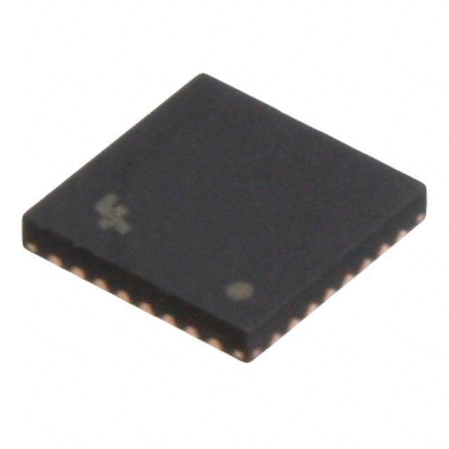
| 描述 | IC TXRX CAN 8DFNCAN 接口集成电路 |
| 产品分类 | |
| 品牌 | Microchip Technology |
| 产品手册 | |
| 产品图片 |
|
| rohs | 符合RoHS无铅 / 符合限制有害物质指令(RoHS)规范要求 |
| 产品系列 | 接口 IC,CAN 接口集成电路,Microchip Technology MCP2562-E/MF- |
| 数据手册 | http://www.microchip.com/mymicrochip/filehandler.aspx?ddocname=en561044 |
| 产品型号 | MCP2562-E/MF |
| PCN设计/规格 | http://www.microchip.com/mymicrochip/NotificationDetails.aspx?id=6035&print=view |
| 产品种类 | CAN 接口集成电路 |
| 传播延迟时间 | 125 ns |
| 传播延迟时间ns | 125 ns |
| 供应商器件封装 | 8-DFN(3x3) |
| 包装 | 管件 |
| 协议 | CAN |
| 双工 | 全 |
| 商标 | Microchip Technology |
| 安装类型 | 表面贴装 |
| 安装风格 | SMD/SMT |
| 封装 | Tube |
| 封装/外壳 | 8-VDFN 裸露焊盘 |
| 封装/箱体 | DFN-8 |
| 工作温度 | -40°C ~ 125°C |
| 工作温度范围 | - 40 C to + 125 C |
| 工作电源电压 | 1.8 V to 5.5 V |
| 工厂包装数量 | 120 |
| 接收器滞后 | - |
| 数据速率 | 1 Mbps |
| 最大工作温度 | + 125 C |
| 最小工作温度 | - 40 C |
| 标准包装 | 120 |
| 电压-电源 | 4.5 V ~ 5.5 V |
| 电源电压-最大 | 5.5 V |
| 电源电压-最小 | 1.8 V |
| 电源电流 | 70 mA |
| 类型 | CAN Transceiver |
| 驱动器/接收器数 | 1/1 |


- 商务部:美国ITC正式对集成电路等产品启动337调查
- 曝三星4nm工艺存在良率问题 高通将骁龙8 Gen1或转产台积电
- 太阳诱电将投资9.5亿元在常州建新厂生产MLCC 预计2023年完工
- 英特尔发布欧洲新工厂建设计划 深化IDM 2.0 战略
- 台积电先进制程称霸业界 有大客户加持明年业绩稳了
- 达到5530亿美元!SIA预计今年全球半导体销售额将创下新高
- 英特尔拟将自动驾驶子公司Mobileye上市 估值或超500亿美元
- 三星加码芯片和SET,合并消费电子和移动部门,撤换高东真等 CEO
- 三星电子宣布重大人事变动 还合并消费电子和移动部门
- 海关总署:前11个月进口集成电路产品价值2.52万亿元 增长14.8%


PDF Datasheet 数据手册内容提取
MCP2561/2 High-Speed CAN Transceiver Features: Description: • Supports 1 Mb/s Operation The MCP2561/2 is a Microchip Technology Inc. second • Implements ISO-11898-2 and ISO-11898-5 generation high-speed CAN transceiver. It serves as an Standard Physical Layer Requirements interface between a CAN protocol controller and the physical two-wire CAN bus. • Very Low Standby Current (5 µA, typical) • VIO Supply Pin to Interface Directly to The device meets the automotive requirements for CAN Controllers and Microcontrollers with high-speed (up to 1 Mb/s), low quiescent current, 1.8V to 5.5V I/O electromagnetic compatibility (EMC) and electrostatic discharge (ESD). • SPLIT Output Pin to Stabilize Common Mode in Biased Split Termination Schemes Package Types • CAN Bus Pins are Disconnected when Device is Unpowered: MCP2561 MCP2562 - An Unpowered Node or Brown-Out Event will PDIP, SOIC PDIP, SOIC Not Load the CAN Bus TXD 1 8 STBY TXD 1 8 STBY • Detection of Ground Fault: VSS 2 7 CANH VSS 2 7 CANH - Permanent Dominant Detection on TXD VDD 3 6 CANL VDD 3 6 CANL - Permanent Dominant Detection on Bus RXD 4 5 SPLIT RXD 4 5 VIO • Power-on Reset and Voltage Brown-Out Protection on VDD Pin MCP2561 MCP2562 • Protection Against Damage Due to Short-Circuit 3x3 DFN* 3x3 DFN* Conditions (Positive or Negative Battery Voltage) • Protection Against High-Voltage Transients in TXD 1 8 STBY TXD 1 8 STBY Automotive Environments VSS 2 EP 7 CANH VSS 2 EP 7 CANH • Automatic Thermal Shutdown Protection VDD 3 9 6 CANL VDD 3 9 6 CANL • Suitable for 12V and 24V Systems RXD 4 5 SPLIT RXD 4 5 VIO • Meets or exceeds stringent automotive design * Includes Exposed Thermal Pad (EP); see Table 1-2. requirements including “Hardware Requirements for LIN, CAN and FlexRay Interfaces in Automo- tive Applications”, Version 1.3, May 2012 • High-Noise Immunity Due to Differential Bus Implementation • High Electrostatic Discharge (ESD) Protection on CANH and CANL, meeting the IEC61000-4-2 up to ±14 kV • Available in PDIP-8L, SOIC-8L and 3x3 DFN-8L • Temperature ranges: - Extended (E): -40°C to +125°C - High (H): -40°C to +150°C MCP2561/2 Family Members Device Feature Description MCP2561 Split pin Common mode stabilization MCP2562 VIO pin Internal level shifter on digital I/O pins Note: For ordering information, see the “Product Identification System” section on page 27. 2013-2014 Microchip Technology Inc. DS20005167C-page 1
MCP2561/2 Block Diagram SPLIT(2 ) VIO(3) VDD DigitalI/O Thermal POR VDD/2 Supply Protection UVLO VIO Permanent TXD DominantDetect Driver CANH VIO and SlopeControl CANL Mode STBY Control CANH Wake-Up LP_RX(1) Filter CANL Receiver RXD CANH HS_RX CANL VSS Note1: There is only one receiver implemented. The receiver can operate in Low-Power or High-Speed mode. 2: Only MCP2561 has the SPLIT pin. 3: Only MCP2562 has the VIO pin. In MCP2561, the supply for the digital I/O is internally connected to VDD. DS20005167C-page 2 2013-2014 Microchip Technology Inc.
MCP2561/2 1.0 DEVICE OVERVIEW 1.1.1 NORMAL MODE Normal mode is selected by applying a low-level to the The MCP2561/2 is a high-speed CAN, fault-tolerant STBY pin. The driver block is operational and can drive device that serves as the interface between a CAN the bus pins. The slopes of the output signals on CANH protocol controller and the physical bus. The and CANL are optimized to produce minimal MCP2561/2 device provides differential transmit and electromagnetic emissions (EME). receive capability for the CAN protocol controller, and is fully compatible with the ISO-11898-2 and The high-speed differential receiver is active. ISO-11898-5 standards. It will operate at speeds of up to 1 Mb/s. 1.1.2 STANDBY MODE Typically, each node in a CAN system must have a The device may be placed in Standby mode by device to convert the digital signals generated by a applying a high-level to the STBY pin. In Standby CAN controller to signals suitable for transmission over mode, the transmitter and the high-speed part of the the bus cabling (differential output). It also provides a receiver are switched off to minimize power buffer between the CAN controller and the high-voltage consumption. The low-power receiver and the wake-up spikes that can be generated on the CAN bus by filter blocks are enabled in order to monitor the bus for outside sources. activity. The receive pin (RXD) will show a delayed representation of the CAN bus, due to the wake-up 1.1 Mode Control Block filter. The CAN controller gets interrupted by a negative edge The MCP2561/2 supports two modes of operation: on the RXD pin (dominant state on the CAN bus). The • Normal CAN controller must put the MCP2561/2 back into • Standby Normal mode using the STBY pin, in order to enable high-speed data communication. These modes are summarized in Table 1-1. The CAN bus wake-up function requires both supply voltages, VDD and VIO, to be in valid range. TABLE 1-1: MODES OF OPERATION RXD Pin Mode STBY Pin LOW HIGH Normal LOW Bus is dominant Bus is recessive Standby HIGH Wake-up request is detected No wake-up request detected 1.2 Transmitter Function 1.4 Internal Protection The CAN bus has two states: Dominant and CANH and CANL are protected against battery short- Recessive. A Dominant state occurs when the circuits and electrical transients that can occur on the differential voltage between CANH and CANL is CAN bus. This feature prevents destruction of the greater than VDIFF(D)(I). A Recessive state occurs transmitter output stage during such a Fault condition. when the differential voltage is less than VDIFF(R)(I). The device is further protected from excessive current The Dominant and Recessive states correspond to the loading by thermal shutdown circuitry that disables the Low and High state of the TXD input pin, respectively. output drivers when the junction temperature exceeds However, a Dominant state initiated by another CAN a nominal limit of +175°C. All other parts of the chip node will override a Recessive state on the CAN bus. remain operational, and the chip temperature is low- ered due to the decreased power dissipation in the 1.3 Receiver Function transmitter outputs. This protection is essential to protect against bus line short-circuit-induced damage. In Normal mode, the RXD output pin reflects the differ- ential bus voltage between CANH and CANL. The Low and High states of the RXD output pin correspond to the Dominant and Recessive states of the CAN bus, respectively. 2013-2014 Microchip Technology Inc. DS20005167C-page 3
MCP2561/2 1.5 Permanent Dominant Detection 1.6 Power-On Reset (POR) and Undervoltage Detection The MCP2561/2 device prevents two conditions: • Permanent dominant condition on TXD The MCP2561/2 has undervoltage detection on both • Permanent dominant condition on the bus supply pins: VDD and VIO. Typical undervoltage thresholds are 1.2V for VIO and 4V for VDD. In Normal mode, if the MCP2561/2 detects an When the device is powered on, CANH and CANL extended Low state on the TXD input, it will disable the CANH and CANL output drivers in order to prevent the remain in a high-impedance state until both VDD and corruption of data on the CAN bus. The drivers will VIO exceed their undervoltage levels. Once powered on, CANH and CANL will enter a high-impedance state remain disabled until TXD goes High. if the voltage level at VDD drops below the undervoltage In Standby mode, if the MCP2561/2 detects an level, providing voltage brown-out protection during extended dominant condition on the bus, it will set the normal operation. RXD pin to Recessive state. This allows the attached In Normal mode, the receiver output is forced to controller to go to Low-Power mode until the dominant Recessive state during an undervoltage condition on issue is corrected. RXD is latched High until a Recessive state is detected on the bus, and the VDD. In Standby mode, the low-power receiver is only wake-up function is enabled again. enabled when both VDD and VIO supply voltages rise above their respective undervoltage thresholds. Once Both conditions have a time-out of 1.25 ms (typical). these threshold voltages are reached, the low-power This implies a maximum bit time of 69.44 µs receiver is no longer controlled by the POR comparator (14.4 kHz), allowing up to 18 consecutive dominant bits and remains operational down to about 2.5V on the on the bus. VDD supply (MCP2561/2). The MCP2562 transfers data to the RXD pin down to 1.8V on the VIO supply. 1.7 Pin Descriptions Table 1-2 describes the pinout. TABLE 1-2: MCP2561/2 PINOUT MCP2561 MCP2561 MCP2562 MCP2562 Symbol Pin Function 3x3 DFN PDIP, SOIC 3x3 DFN PDIP, SOIC 1 1 1 1 TXD Transmit Data Input 2 2 2 2 VSS Ground 3 3 3 3 VDD Supply Voltage 4 4 4 4 RXD Receive Data Output 5 5 — — SPLIT Common Mode Stabilization – MCP2561 only — — 5 5 VIO Digital I/O Supply Pin – MCP2562 only 6 6 6 6 CANL CAN Low-Level Voltage I/O 7 7 7 7 CANH CAN High-Level Voltage I/O 8 8 8 8 STBY Standby Mode Input 9 — 9 — EP Exposed Thermal Pad DS20005167C-page 4 2013-2014 Microchip Technology Inc.
MCP2561/2 1.7.1 TRANSMITTER DATA 1.7.9 STANDBY MODE INPUT PIN (STBY) INPUT PIN (TXD) This pin selects between Normal or Standby mode. In The CAN transceiver drives the differential output pins Standby mode, the transmitter, high speed receiver and CANH and CANL according to TXD. It is usually SPLIT are turned off, only the low power receiver and connected to the transmitter data output of the CAN wake-up filter are active. STBY is connected to an controller device. When TXD is Low, CANH and CANL internal MOS pull-up resistor to VDD or VIO, in the are in the Dominant state. When TXD is High, CANH MCP2561 or MCP2562, respectively. The value of the and CANL are in the Recessive state, provided that MOS pull-up resistor depends on the supply voltage. another CAN node is not driving the CAN bus with a Typical values are 660 k for 5V, 1.1 M for 3.3V and Dominant state. TXD is connected to an internal pull-up 4.4 M for 1.8V resistor (nominal 33 k) to VDD or VIO, in the MCP2561 1.7.10 EXPOSED THERMAL PAD (EP) or MCP2562, respectively. It is recommended to connect this pad to VSS to 1.7.2 GROUND SUPPLY PIN (VSS) enhance electromagnetic immunity and thermal Ground supply pin. resistance. 1.7.3 SUPPLY VOLTAGE PIN (VDD) Positive supply voltage pin. Supplies transmitter and receiver, including the wake-up receiver. 1.7.4 RECEIVER DATA OUTPUT PIN (RXD) RXD is a CMOS-compatible output that drives High or Low depending on the differential signals on the CANH and CANL pins, and is usually connected to the receiver data input of the CAN controller device. RXD is High when the CAN bus is Recessive, and Low in the Dominant state. RXD is supplied by VDD or VIO, in the MCP2561 or MCP2562, respectively. 1.7.5 SPLIT PIN (MCP2561 ONLY) Reference Voltage Output (defined as VDD/2). The pin is only active in Normal mode. In Standby mode, or when VDD is off, SPLIT floats. 1.7.6 VIO PIN (MCP2562 ONLY) Supply for digital I/O pins. In the MCP2561, the supply for the digital I/O (TXD, RXD and STBY) is internally connected to VDD. 1.7.7 CAN LOW PIN (CANL) The CANL output drives the Low side of the CAN differential bus. This pin is also tied internally to the receive input comparator. CANL disconnects from the bus when MCP2561/2 is not powered. 1.7.8 CAN HIGH PIN (CANH) The CANH output drives the high-side of the CAN differential bus. This pin is also tied internally to the receive input comparator. CANH disconnects from the bus when MCP2561/2 is not powered. 2013-2014 Microchip Technology Inc. DS20005167C-page 5
MCP2561/2 1.8 Typical Applications FIGURE 1-1: MCP2561 WITH SPLIT PIN VBAT 5V LDO 0.1 μF VDD VDDCANH CANH CANTX TXD 1 PIC® 56 300(cid:58) 60(cid:58) MCU CANRX RXD P2 SPLIT C 4700 pF RBX STBY M Optional(1) 60(cid:58) CANL CANL VSS VSS Note 1: Optional resistor to allow communication during bus failure (CANL shorted to ground). FIGURE 1-2: MCP2562 WITH VIO PIN VBAT 5V LDO 1.8V LDO 0.1 μF 0.1 μF VDD VIO VDD CANH CANTX TXD 2 CANH PIC® 56 MCU CANRX RXD P2 120(cid:58) C RBX STBY M CANL CANL VSS Vss DS20005167C-page 6 2013-2014 Microchip Technology Inc.
MCP2561/2 2.0 ELECTRICAL 2.1.5 DIFFERENTIAL VOLTAGE, VDIFF CHARACTERISTICS (OF CAN BUS) Differential voltage of the two-wire CAN bus, value 2.1 Terms and Definitions VDIFF = VCANH – VCANL. A number of terms are defined in ISO-11898 that are 2.1.6 INTERNAL CAPACITANCE, CIN used to describe the electrical characteristics of a CAN (OF A CAN NODE) transceiver device. These terms and definitions are Capacitance seen between CANL (or CANH) and summarized in this section. ground during the Recessive state, when the CAN 2.1.1 BUS VOLTAGE node is disconnected from the bus (see Figure 2-1). VCANL and VCANH denote the voltages of the bus line 2.1.7 INTERNAL RESISTANCE, RIN wires CANL and CANH relative to ground of each (OF A CAN NODE) individual CAN node. Resistance seen between CANL (or CANH) and 2.1.2 COMMON MODE BUS VOLTAGE ground during the Recessive state, when the CAN RANGE node is disconnected from the bus (see Figure 2-1). Boundary voltage levels of VCANL and VCANH with FIGURE 2-1: PHYSICAL LAYER respect to ground, for which proper operation will occur, DEFINITIONS if up to the maximum number of CAN nodes are connected to the bus. ECU 2.1.3 DIFFERENTIAL INTERNAL CAPACITANCE, CDIFF RIN (OF A CAN NODE) CANL Capacitance seen between CANL and CANH during RDIFF CDIFF the Recessive state, when the CAN node is RIN disconnected from the bus (see Figure 2-1). CANH CIN CIN 2.1.4 DIFFERENTIAL INTERNAL GROUND RESISTANCE, RDIFF (OF A CAN NODE) Resistance seen between CANL and CANH during the Recessive state when the CAN node is disconnected from the bus (see Figure 2-1). 2013-2014 Microchip Technology Inc. DS20005167C-page 7
MCP2561/2 Absolute Maximum Ratings† VDD.............................................................................................................................................................................7.0V VIO..............................................................................................................................................................................7.0V DC Voltage at TXD, RXD, STBY and VSS.............................................................................................-0.3V to VIO + 0.3V DC Voltage at CANH, CANL and SPLIT......................................................................................................-58V to +58V Transient Voltage on CANH, CANL (ISO-7637) (Figure 2-5)...................................................................-150V to +100V Storage temperature...............................................................................................................................-55°C to +150°C Operating ambient temperature..............................................................................................................-40°C to +150°C Virtual Junction Temperature, TVJ (IEC60747-1)....................................................................................-40°C to +190°C Soldering temperature of leads (10 seconds).......................................................................................................+300°C ESD protection on CANH and CANL pins for MCP2561 (IEC 61000-4-2).............................................................±14 kV ESD protection on CANH and CANL pins for MCP2562 (IEC 61000-4-2)...............................................................±8 kV ESD protection on CANH and CANL pins (IEC 801; Human Body Model)..............................................................±8 kV ESD protection on all other pins (IEC 801; Human Body Model).............................................................................±4 kV ESD protection on all pins (IEC 801; Machine Model)............................................................................................±300V ESD protection on all pins (IEC 801; Charge Device Model)..................................................................................±750V † NOTICE: Stresses above those listed under “Maximum ratings” may cause permanent damage to the device. This is a stress rating only and functional operation of the device at those or any other conditions above those indicated in the operational listings of this specification is not implied. Exposure to maximum rating conditions for extended periods may affect device reliability. DS20005167C-page 8 2013-2014 Microchip Technology Inc.
MCP2561/2 2.2 DC Characteristics Electrical Characteristics: Extended (E): TAMB = -40°C to +125°C and High (H): TAMB = -40°C to +150°C; VDD = 4.5V to 5.5V, VIO = 1.8V to 5.5V (Note 2), RL = 60; unless otherwise specified. Characteristic Sym. Min. Typ. Max. Units Conditions SUPPLY VDD Pin Voltage Range VDD 4.5 — 5.5 Supply Current IDD — 5 10 mA Recessive; VTXD = VDD — 45 70 Dominant; VTXD = 0V Standby Current IDDS — 5 15 µA MCP2561 — 5 15 MCP2562; Includes IIO High Level of the POR VPORH 3.8 — 4.3 V Comparator Low Level of the POR VPORL 3.4 — 4.0 V Comparator Hysteresis of POR VPORD 0.3 — 0.8 V Comparator V Pin IO Digital Supply Voltage Range VIO 1.8 — 5.5 V Supply Current on VIO IIO — 4 30 µA Recessive; VTXD = VIO — 85 500 Dominant; VTXD = 0V Standby Current IDDS — 0.3 1 µA (Note 1) Undervoltage detection on VIO VUVD(IO) — 1.2 — V (Note 1) BUS LINE (CANH; CANL) TRANSMITTER CANH; CANL: VO(R) 2.0 0.5VDD 3.0 V VTXD = VDD; No load Recessive Bus Output Voltage CANH; CANL: VO(S) -0.1 0.0 +0.1 V STBY = VTXD = VDD; No load Bus Output Voltage in Standby Recessive Output Current IO(R) -5 — +5 mA -24V < VCAN < +24V CANH: Dominant VO(D) 2.75 3.50 4.50 V TXD = 0; RL = 50 to 65 Output Voltage CANL: Dominant 0.50 1.50 2.25 RL = 50 to 65 Output Voltage Symmetry of Dominant VO(D)(M) -400 0 +400 mV VTXD = VSS (Note 1) Output Voltage (VDD – VCANH – VCANL) Dominant: Differential VO(DIFF) 1.5 2.0 3.0 V VTXD = VSS; RL = 50 to 65 Output Voltage Figure 2-2, Figure 2-4 Recessive: -120 0 12 mV VTXD = VDD Differential Output Voltage Figure 2-2, Figure 2-4 -500 0 50 mV VTXD = VDD,no load. Figure 2-2, Figure 2-4 Note 1: Characterized; not 100% tested. 2: Only MCP2562 has VIO pin. For the MCP2561, VIO is internally connected to VDD. 3: -12V to 12V is ensured by characterization, tested from -2V to 7V. 2013-2014 Microchip Technology Inc. DS20005167C-page 9
MCP2561/2 2.2 DC Characteristics (Continued) Electrical Characteristics: Extended (E): TAMB = -40°C to +125°C and High (H): TAMB = -40°C to +150°C; VDD = 4.5V to 5.5V, VIO = 1.8V to 5.5V (Note 2), RL = 60; unless otherwise specified. Characteristic Sym. Min. Typ. Max. Units Conditions CANH: Short Circuit IO(SC) -120 -85 — mA VTXD = VSS; VCANH = 0V; Output Current CANL: floating -100 — — mA same as above, but VDD=5V, TAMB = +25°C (Note 1) CANL: Short Circuit — 75 +120 mA VTXD = VSS; VCANL = 18V; Output Current CANH: floating — — +100 mA same as above, but VDD=5V, TAMB = +25°C (Note 1) BUS LINE (CANH; CANL) RECEIVER Recessive Differential VDIFF(R)(I) -1.0 — +0.5 V Normal Mode; Input Voltage -12V < V(CANH, CANL) < +12V; See Figure 2-6 (Note 3) -1.0 — +0.4 Standby Mode; -12V < V(CANH, CANL) < +12V; See Figure 2-6 (Note 3) Dominant Differential VDIFF(D)(I) 0.9 — VDD V Normal Mode; Input Voltage -12V < V(CANH, CANL) < +12V; See Figure 2-6 (Note 3) 1.0 — VDD Standby Mode; -12V < V(CANH, CANL) < +12V; See Figure 2-6 (Note 3) Differential VTH(DIFF) 0.5 0.7 0.9 V Normal Mode; Receiver Threshold -12V < V(CANH, CANL) < +12V; See Figure 2-6 (Note 3) 0.4 — 1.15 Standby Mode; -12V < V(CANH, CANL) < +12V; See Figure 2-6 (Note 3) Differential VHYS(DIFF) 50 — 200 mV Normal mode, see Figure 2-6, Input Hysteresis (Note 1) Common Mode RIN 10 — 30 k (Note 1) Input Resistance Common Mode RIN(M) -1 0 +1 % VCANH = VCANL, (Note 1) Resistance Matching Differential Input RIN(DIFF) 10 — 100 k (Note 1) Resistance Common Mode CIN(CM) — — 20 pF VTXD = VDD; (Note 1) Input Capacitance Differential CIN(DIFF) — — 10 VTXD = VDD; (Note 1) Input Capacitance CANH, CANL: ILI -5 — +5 µA VDD = VTXD = VSTBY = 0V. Input Leakage For MCP2562, VIO = 0V. VCANH = VCANL = 5 V. Note 1: Characterized; not 100% tested. 2: Only MCP2562 has VIO pin. For the MCP2561, VIO is internally connected to VDD. 3: -12V to 12V is ensured by characterization, tested from -2V to 7V. DS20005167C-page 10 2013-2014 Microchip Technology Inc.
MCP2561/2 2.2 DC Characteristics (Continued) Electrical Characteristics: Extended (E): TAMB = -40°C to +125°C and High (H): TAMB = -40°C to +150°C; VDD = 4.5V to 5.5V, VIO = 1.8V to 5.5V (Note 2), RL = 60; unless otherwise specified. Characteristic Sym. Min. Typ. Max. Units Conditions COMMON MODE STABILIZATION OUTPUT (SPLIT) Output Voltage Vo 0.3VDD 0.5VDD 0.7VDD V Normal mode; ISPLIT = -500 µA to +500 µA 0.45VDD 0.5VDD 0.55VDD V Normal mode; RL 1 M Leakage Current I -5 — +5 µA Standby mode; L VSPLIT = -24V to + 24V (ISO 11898: -12V ~ +12V) DIGITAL INPUT PINS (TXD, STBY) High-Level Input Voltage VIH 0.7VIO — VIO + 0.3 V Low-Level Input Voltage VIL -0.3 — 0.3VIO V High-Level Input Current I -1 — +1 µA IH TXD: Low-Level Input Current IIL(TXD) -270 -150 -30 µA STBY: Low-Level Input Current I -30 — -1 µA IL(STBY) RECEIVE DATA (RXD) OUTPUT High-Level Output Voltage VOH VDD - 0.4 — — V IOH = -2 mA (MCP2561); typical -4 mA VIO - 0.4 — — IOH = -1 mA (MCP2562); typical -2 mA Low-Level Output Voltage VOL — — 0.4 V IOL = 4 mA; typical 8 mA THERMAL SHUTDOWN Shutdown TJ(SD) 165 175 185 °C -12V < V(CANH, CANL) < +12V, Junction Temperature (Note 1) Shutdown TJ(HYST) 20 — 30 °C -12V < V(CANH, CANL) < +12V, Temperature Hysteresis (Note 1) Note 1: Characterized; not 100% tested. 2: Only MCP2562 has VIO pin. For the MCP2561, VIO is internally connected to VDD. 3: -12V to 12V is ensured by characterization, tested from -2V to 7V. 2013-2014 Microchip Technology Inc. DS20005167C-page 11
MCP2561/2 FIGURE 2-2: PHYSICAL BIT REPRESENTATION AND SIMPLIFIED BIAS IMPLEMENTATION NormalMode StandbyMode T CANH LI P S L, N SPLIT SPLIT A C floating H, N A C CANL Recessive Dominant Recessive Time VDD CANH VDD/2 Normal RXD Standby Mode CANL DS20005167C-page 12 2013-2014 Microchip Technology Inc.
MCP2561/2 2.3 AC Characteristics Electrical Characteristics: Extended (E): TAMB = -40°C to +125°C and High (H): TAMB = -40°C to +150°C; VDD = 4.5V to 5.5V, VIO = 1.8V to 5.5V (Note 2), RL = 60; unless otherwise specified. Param. Sym. Characteristic Min. Typ. Max. Units Conditions No. 1 tBIT Bit Time 1 — 69.44 µs 2 fBIT Bit Frequency 14.4 — 1000 kHz 3 tTXD-BUSON Delay TXD Low to Bus Dominant — — 70 ns 4 tTXD-BUSOFF Delay TXD High to Bus Recessive — — 125 ns 5 tBUSON-RXD Delay Bus Dominant to RXD — — 70 ns 6 tBUSOFF-RXD Delay Bus Recessive to RXD — — 110 ns 7 tTXD - RXD Propagation Delay TXD to RXD — — 125 ns Negative edge on TXD 8 — — 235 Positive edge on TXD 9 tFLTR(WAKE) Delay Bus Dominant to RXD 0.5 1 4 µs Standby mode (Standby mode) 10 tWAKE Delay Standby 5 25 40 µs Negative edge on STBY to Normal Mode 11 tPDT Permanent Dominant Detect Time — 1.25 — ms TXD = 0V 12 tPDTR Permanent Dominant Timer Reset — 100 — ns The shortest recessive pulse on TXD or CAN bus to reset Permanent Dominant Timer FIGURE 2-3: TEST LOAD CONDITIONS Load Condition 1 Load Condition 2 VDD/2 RL Pin CL Pin CL RL = 464 CL = 50 pF for all digital pins VSS VSS FIGURE 2-4: TEST CIRCUIT FOR ELECTRICAL CHARACTERISTICS 0.1µF V DD CANH TXD SPLIT CAN RL 100pF Transceiver RXD CANL 30pF GND STBY Note: On MCP2562, VIO is connected to VDD. 2013-2014 Microchip Technology Inc. DS20005167C-page 13
MCP2561/2 FIGURE 2-5: TEST CIRCUIT FOR AUTOMOTIVE TRANSIENTS 1000pF CANH TXD Transient SPLIT CAN RL Generator Transceiver RXD CANL 1000pF GND STBY Note: On MCP2562, VIO is connected to VDD. The wave forms of the applied transients shall be in accordance with ISO-7637, Part 1, test pulses 1, 2, 3a and 3b. FIGURE 2-6: HYSTERESIS OF THE RECEIVER RXD (receive data VOH output voltage) VDIFF (r)(i) VDIFF (d)(i) VOL VDIFF (h)(i) 0.5 VDIFF (V) 0.9 DS20005167C-page 14 2013-2014 Microchip Technology Inc.
MCP2561/2 2.4 Timing Diagrams and Specifications FIGURE 2-7: TIMING DIAGRAM FOR AC CHARACTERISTICS VDD TXD (transmit data input voltage) 0V VDIFF (CANH, CANL differential voltage) RXD (receive data output voltage) 3 5 7 4 6 8 FIGURE 2-8: TIMING DIAGRAM FOR WAKE-UP FROM STANDBY VSTBY VDD Input Voltage 0V VDD/2 VCANH/VCANL 0 VTXD = VDD 10 FIGURE 2-9: PERMANENT DOMINANT TIMER RESET DETECT Minimum pulse width until CAN bus goes to dominant after the falling edge TXD VDIFF (VCANH-VCANL) Driver is off 11 12 2013-2014 Microchip Technology Inc. DS20005167C-page 15
MCP2561/2 2.5 Thermal Specifications Parameter Symbol Min. Typ. Max. Units Test Conditions Temperature Ranges Specified Temperature Range TA -40 — +125 C -40 — +150 Operating Temperature Range TA -40 — +150 C Storage Temperature Range TA -65 — +155 C Thermal Package Resistances Thermal Resistance, 8L-DFN 3x3 JA — 56.7 — C/W Thermal Resistance, 8L-PDIP JA — 89.3 — C/W Thermal Resistance, 8L-SOIC JA — 149.5 — C/W DS20005167C-page 16 2013-2014 Microchip Technology Inc.
MCP2561/2 3.0 PACKAGING INFORMATION 3.1 Package Marking Information 8-Lead DFN (3x3 mm) Example: Part Number Code MCP2561-E/MF DADR MCP2561T-E/MF DADR DADR 1326 MCP2561-H/MF DADS 256 MCP2561T-H/MF DADS MCP2562-E/MF DADU MCP2562T-E/MF DADU MCP2562-H/MF DADT MCP2562T-H/MF DADT 8-Lead PDIP (300 mil) Example: XXXXXXXX XXXXXNNN MCP2561 OR MCP2561 E/P e^3^256 H/P e^3^256 YYWW 1307 1307 8-Lead PDIP (300 mil) Example: 8-Lead SOIC (150 mil) Example: MCP2561E MCP2561H SN e^3^1246 OR SN e^3^1246 NNN 256 256 Legend: XX...X Customer-specific information Y Year code (last digit of calendar year) YY Year code (last 2 digits of calendar year) WW Week code (week of January 1 is week ‘01’) NNN Alphanumeric traceability code e3 Pb-free JEDEC® designator for Matte Tin (Sn) * This package is Pb-free. The Pb-free JEDEC designator (e 3 ) can be found on the outer packaging for this package. Note: In the event the full Microchip part number cannot be marked on one line, it will be carried over to the next line, thus limiting the number of available characters for customer-specific information. 2013-2014 Microchip Technology Inc. DS20005167C-page 17
MCP2561/2 Note: For the most current package drawings, please see the Microchip Packaging Specification located at http://www.microchip.com/packaging DS20005167C-page 18 2013-2014 Microchip Technology Inc.
MCP2561/2 Note: For the most current package drawings, please see the Microchip Packaging Specification located at http://www.microchip.com/packaging 2013-2014 Microchip Technology Inc. DS20005167C-page 19
MCP2561/2 Note: For the most current package drawings, please see the Microchip Packaging Specification located at http://www.microchip.com/packaging DS20005167C-page 20 2013-2014 Microchip Technology Inc.
MCP2561/2 (cid:2)(cid:3)(cid:4)(cid:5)(cid:6)(cid:7)(cid:8)(cid:9)(cid:10)(cid:6)(cid:11)(cid:12)(cid:13)(cid:14)(cid:8)(cid:15)(cid:16)(cid:6)(cid:10)(cid:8)(cid:17)(cid:18)(cid:3)(cid:4)(cid:13)(cid:18)(cid:5)(cid:8)(cid:19)(cid:9)(cid:20)(cid:8)(cid:21)(cid:8)(cid:22)(cid:23)(cid:23)(cid:8)(cid:24)(cid:13)(cid:10)(cid:8)(cid:25)(cid:26)(cid:7)(cid:27)(cid:8)(cid:28)(cid:9)(cid:15)(cid:17)(cid:9)(cid:29) (cid:30)(cid:26)(cid:12)(cid:5)(cid:31) 3(cid:10)(cid:9)(cid:2)&(cid:11)(cid:14)(cid:2)’(cid:10)!&(cid:2)(cid:8)"(cid:9)(cid:9)(cid:14)(cid:15)&(cid:2)(cid:12)(cid:28)(cid:8)4(cid:28)(cid:17)(cid:14)(cid:2)#(cid:9)(cid:28)*(cid:7)(cid:15)(cid:17)!((cid:2)(cid:12)(cid:16)(cid:14)(cid:28)!(cid:14)(cid:2)!(cid:14)(cid:14)(cid:2)&(cid:11)(cid:14)(cid:2)(cid:6)(cid:7)(cid:8)(cid:9)(cid:10)(cid:8)(cid:11)(cid:7)(cid:12)(cid:2)(cid:31)(cid:28)(cid:8)4(cid:28)(cid:17)(cid:7)(cid:15)(cid:17)(cid:2)(cid:22)(cid:12)(cid:14)(cid:8)(cid:7)%(cid:7)(cid:8)(cid:28)&(cid:7)(cid:10)(cid:15)(cid:2)(cid:16)(cid:10)(cid:8)(cid:28)&(cid:14)#(cid:2)(cid:28)&(cid:2) (cid:11)&&(cid:12)255***(cid:20)’(cid:7)(cid:8)(cid:9)(cid:10)(cid:8)(cid:11)(cid:7)(cid:12)(cid:20)(cid:8)(cid:10)’5(cid:12)(cid:28)(cid:8)4(cid:28)(cid:17)(cid:7)(cid:15)(cid:17) N NOTE1 E1 1 2 3 D E A A2 L A1 c e eB b1 b 6(cid:15)(cid:7)&! (cid:19)7,8.(cid:22) (cid:21)(cid:7)’(cid:14)(cid:15)!(cid:7)(cid:10)(cid:15)(cid:2)9(cid:7)’(cid:7)&! (cid:6)(cid:19)7 7:(cid:6) (cid:6)(cid:25); 7"’)(cid:14)(cid:9)(cid:2)(cid:10)%(cid:2)(cid:31)(cid:7)(cid:15)! 7 < (cid:31)(cid:7)&(cid:8)(cid:11) (cid:14) (cid:20)(cid:30)(cid:4)(cid:4)(cid:2)1(cid:22), (cid:13)(cid:10)(cid:12)(cid:2)&(cid:10)(cid:2)(cid:22)(cid:14)(cid:28)&(cid:7)(cid:15)(cid:17)(cid:2)(cid:31)(cid:16)(cid:28)(cid:15)(cid:14) (cid:25) = = (cid:20)(cid:3)(cid:30)(cid:4) (cid:6)(cid:10)(cid:16)#(cid:14)#(cid:2)(cid:31)(cid:28)(cid:8)4(cid:28)(cid:17)(cid:14)(cid:2)(cid:13)(cid:11)(cid:7)(cid:8)4(cid:15)(cid:14)!! (cid:25)(cid:3) (cid:20)(cid:30)(cid:30)(cid:29) (cid:20)(cid:30)-(cid:4) (cid:20)(cid:30)(cid:24)(cid:29) 1(cid:28)!(cid:14)(cid:2)&(cid:10)(cid:2)(cid:22)(cid:14)(cid:28)&(cid:7)(cid:15)(cid:17)(cid:2)(cid:31)(cid:16)(cid:28)(cid:15)(cid:14) (cid:25)(cid:30) (cid:20)(cid:4)(cid:30)(cid:29) = = (cid:22)(cid:11)(cid:10)"(cid:16)#(cid:14)(cid:9)(cid:2)&(cid:10)(cid:2)(cid:22)(cid:11)(cid:10)"(cid:16)#(cid:14)(cid:9)(cid:2)>(cid:7)#&(cid:11) . (cid:20)(cid:3)(cid:24)(cid:4) (cid:20)-(cid:30)(cid:4) (cid:20)-(cid:3)(cid:29) (cid:6)(cid:10)(cid:16)#(cid:14)#(cid:2)(cid:31)(cid:28)(cid:8)4(cid:28)(cid:17)(cid:14)(cid:2)>(cid:7)#&(cid:11) .(cid:30) (cid:20)(cid:3)(cid:23)(cid:4) (cid:20)(cid:3)(cid:29)(cid:4) (cid:20)(cid:3)<(cid:4) : (cid:14)(cid:9)(cid:28)(cid:16)(cid:16)(cid:2)9(cid:14)(cid:15)(cid:17)&(cid:11) (cid:21) (cid:20)-(cid:23)< (cid:20)-?(cid:29) (cid:20)(cid:23)(cid:4)(cid:4) (cid:13)(cid:7)(cid:12)(cid:2)&(cid:10)(cid:2)(cid:22)(cid:14)(cid:28)&(cid:7)(cid:15)(cid:17)(cid:2)(cid:31)(cid:16)(cid:28)(cid:15)(cid:14) 9 (cid:20)(cid:30)(cid:30)(cid:29) (cid:20)(cid:30)-(cid:4) (cid:20)(cid:30)(cid:29)(cid:4) 9(cid:14)(cid:28)#(cid:2)(cid:13)(cid:11)(cid:7)(cid:8)4(cid:15)(cid:14)!! (cid:8) (cid:20)(cid:4)(cid:4)< (cid:20)(cid:4)(cid:30)(cid:4) (cid:20)(cid:4)(cid:30)(cid:29) 6(cid:12)(cid:12)(cid:14)(cid:9)(cid:2)9(cid:14)(cid:28)#(cid:2)>(cid:7)#&(cid:11) )(cid:30) (cid:20)(cid:4)(cid:23)(cid:4) (cid:20)(cid:4)?(cid:4) (cid:20)(cid:4)(cid:5)(cid:4) 9(cid:10)*(cid:14)(cid:9)(cid:2)9(cid:14)(cid:28)#(cid:2)>(cid:7)#&(cid:11) ) (cid:20)(cid:4)(cid:30)(cid:23) (cid:20)(cid:4)(cid:30)< (cid:20)(cid:4)(cid:3)(cid:3) : (cid:14)(cid:9)(cid:28)(cid:16)(cid:16)(cid:2)(cid:26)(cid:10)*(cid:2)(cid:22)(cid:12)(cid:28)(cid:8)(cid:7)(cid:15)(cid:17)(cid:2)(cid:2)+ (cid:14)1 = = (cid:20)(cid:23)-(cid:4) (cid:30)(cid:26)(cid:12)(cid:5)(cid:11)(cid:31) (cid:30)(cid:20) (cid:31)(cid:7)(cid:15)(cid:2)(cid:30)(cid:2) (cid:7)!"(cid:28)(cid:16)(cid:2)(cid:7)(cid:15)#(cid:14)$(cid:2)%(cid:14)(cid:28)&"(cid:9)(cid:14)(cid:2)’(cid:28)(cid:18)(cid:2) (cid:28)(cid:9)(cid:18)((cid:2))"&(cid:2)’"!&(cid:2))(cid:14)(cid:2)(cid:16)(cid:10)(cid:8)(cid:28)&(cid:14)#(cid:2)*(cid:7)&(cid:11)(cid:2)&(cid:11)(cid:14)(cid:2)(cid:11)(cid:28)&(cid:8)(cid:11)(cid:14)#(cid:2)(cid:28)(cid:9)(cid:14)(cid:28)(cid:20) (cid:3)(cid:20) +(cid:2)(cid:22)(cid:7)(cid:17)(cid:15)(cid:7)%(cid:7)(cid:8)(cid:28)(cid:15)&(cid:2),(cid:11)(cid:28)(cid:9)(cid:28)(cid:8)&(cid:14)(cid:9)(cid:7)!&(cid:7)(cid:8)(cid:20) -(cid:20) (cid:21)(cid:7)’(cid:14)(cid:15)!(cid:7)(cid:10)(cid:15)!(cid:2)(cid:21)(cid:2)(cid:28)(cid:15)#(cid:2).(cid:30)(cid:2)#(cid:10)(cid:2)(cid:15)(cid:10)&(cid:2)(cid:7)(cid:15)(cid:8)(cid:16)"#(cid:14)(cid:2)’(cid:10)(cid:16)#(cid:2)%(cid:16)(cid:28)!(cid:11)(cid:2)(cid:10)(cid:9)(cid:2)(cid:12)(cid:9)(cid:10)&(cid:9)"!(cid:7)(cid:10)(cid:15)!(cid:20)(cid:2)(cid:6)(cid:10)(cid:16)#(cid:2)%(cid:16)(cid:28)!(cid:11)(cid:2)(cid:10)(cid:9)(cid:2)(cid:12)(cid:9)(cid:10)&(cid:9)"!(cid:7)(cid:10)(cid:15)!(cid:2)!(cid:11)(cid:28)(cid:16)(cid:16)(cid:2)(cid:15)(cid:10)&(cid:2)(cid:14)$(cid:8)(cid:14)(cid:14)#(cid:2)(cid:20)(cid:4)(cid:30)(cid:4)/(cid:2)(cid:12)(cid:14)(cid:9)(cid:2)!(cid:7)#(cid:14)(cid:20) (cid:23)(cid:20) (cid:21)(cid:7)’(cid:14)(cid:15)!(cid:7)(cid:10)(cid:15)(cid:7)(cid:15)(cid:17)(cid:2)(cid:28)(cid:15)#(cid:2)&(cid:10)(cid:16)(cid:14)(cid:9)(cid:28)(cid:15)(cid:8)(cid:7)(cid:15)(cid:17)(cid:2)(cid:12)(cid:14)(cid:9)(cid:2)(cid:25)(cid:22)(cid:6).(cid:2)0(cid:30)(cid:23)(cid:20)(cid:29)(cid:6)(cid:20) 1(cid:22),2(cid:2)1(cid:28)!(cid:7)(cid:8)(cid:2)(cid:21)(cid:7)’(cid:14)(cid:15)!(cid:7)(cid:10)(cid:15)(cid:20)(cid:2)(cid:13)(cid:11)(cid:14)(cid:10)(cid:9)(cid:14)&(cid:7)(cid:8)(cid:28)(cid:16)(cid:16)(cid:18)(cid:2)(cid:14)$(cid:28)(cid:8)&(cid:2) (cid:28)(cid:16)"(cid:14)(cid:2)!(cid:11)(cid:10)*(cid:15)(cid:2)*(cid:7)&(cid:11)(cid:10)"&(cid:2)&(cid:10)(cid:16)(cid:14)(cid:9)(cid:28)(cid:15)(cid:8)(cid:14)!(cid:20) (cid:6)(cid:7)(cid:8)(cid:9)(cid:10)(cid:8)(cid:11)(cid:7)(cid:12)(cid:13)(cid:14)(cid:8)(cid:11)(cid:15)(cid:10)(cid:16)(cid:10)(cid:17)(cid:18)(cid:21)(cid:9)(cid:28)*(cid:7)(cid:15)(cid:17),(cid:4)(cid:23)(cid:27)(cid:4)(cid:30)<1 2013-2014 Microchip Technology Inc. DS20005167C-page 21
MCP2561/2 Note: For the most current package drawings, please see the Microchip Packaging Specification located at http://www.microchip.com/packaging DS20005167C-page 22 2013-2014 Microchip Technology Inc.
MCP2561/2 Note: For the most current package drawings, please see the Microchip Packaging Specification located at http://www.microchip.com/packaging 2013-2014 Microchip Technology Inc. DS20005167C-page 23
MCP2561/2 (cid:2)(cid:3)(cid:4)(cid:5)(cid:6)(cid:7)(cid:8)(cid:9)(cid:10)(cid:6)(cid:11)(cid:12)(cid:13)(cid:14)(cid:8) (cid:24)(cid:6)(cid:10)(cid:10)(cid:8)!(cid:16)(cid:12)(cid:10)(cid:13)(cid:18)(cid:5)(cid:8)(cid:19) (cid:30)(cid:20)(cid:8)(cid:21)(cid:8)(cid:30)(cid:6)""(cid:26)#$(cid:8)(cid:22)%&(cid:23)(cid:8)(cid:24)(cid:24)(cid:8)(cid:25)(cid:26)(cid:7)(cid:27)(cid:8)(cid:28) !(cid:17)’(cid:29) (cid:30)(cid:26)(cid:12)(cid:5)(cid:31) 3(cid:10)(cid:9)(cid:2)&(cid:11)(cid:14)(cid:2)’(cid:10)!&(cid:2)(cid:8)"(cid:9)(cid:9)(cid:14)(cid:15)&(cid:2)(cid:12)(cid:28)(cid:8)4(cid:28)(cid:17)(cid:14)(cid:2)#(cid:9)(cid:28)*(cid:7)(cid:15)(cid:17)!((cid:2)(cid:12)(cid:16)(cid:14)(cid:28)!(cid:14)(cid:2)!(cid:14)(cid:14)(cid:2)&(cid:11)(cid:14)(cid:2)(cid:6)(cid:7)(cid:8)(cid:9)(cid:10)(cid:8)(cid:11)(cid:7)(cid:12)(cid:2)(cid:31)(cid:28)(cid:8)4(cid:28)(cid:17)(cid:7)(cid:15)(cid:17)(cid:2)(cid:22)(cid:12)(cid:14)(cid:8)(cid:7)%(cid:7)(cid:8)(cid:28)&(cid:7)(cid:10)(cid:15)(cid:2)(cid:16)(cid:10)(cid:8)(cid:28)&(cid:14)#(cid:2)(cid:28)&(cid:2) (cid:11)&&(cid:12)255***(cid:20)’(cid:7)(cid:8)(cid:9)(cid:10)(cid:8)(cid:11)(cid:7)(cid:12)(cid:20)(cid:8)(cid:10)’5(cid:12)(cid:28)(cid:8)4(cid:28)(cid:17)(cid:7)(cid:15)(cid:17) DS20005167C-page 24 2013-2014 Microchip Technology Inc.
MCP2561/2 APPENDIX A: REVISION HISTORY Revision C (July 2014) The following is the list of modifications: 1. Added references to ISO-11898-2 throughout the document. 2. Updated Section 1.1.2 “Standby Mode”. Described transition from Standby to Normal mode. Emphasized that wake-up on CAN bus requires both VDD and VIO. 3. Explained that POR and Brown-out are limited to VDD pin in Section 1.6 “Power-On Reset (POR) and Undervoltage Detection”. 4. Updated Section 2.2 “DC Characteristics”. Clarified RL, added CANH/CANL Short Circuit specification for 5V and room temperature. 5. Minor typographical corrections. Revision B (March 2013) • Updated the MCP2561/2 Family Members table on page 1. Revision A (March 2013) • Original Release of this Document. 2013-2014 Microchip Technology Inc. DS20005167C-page 25
MCP2561/2 NOTES: DS20005167C-page 26 2013-2014 Microchip Technology Inc.
MCP2561/2 PRODUCT IDENTIFICATION SYSTEM To order or obtain information, e.g., on pricing or delivery, refer to the factory or the listed sales office. PART NO. -X /XX Examples: Device Temperature Package a) MCP2561-E/MF: Extended Temperature, Range 8LD 3x3 DFN package b) MCP2561T-E/MF:Tape and Reel, Extended Temperature, Device: MCP2561: High-Speed CAN Transceiver with SPLIT 8LD 3x3 DFN package MCP2561T: High-Speed CAN Transceiver with SPLIT c) MCP2561-E/P: Extended Temperature, (Tape and Reel) (DFN and SOIC only) 8LD PDIP package MCP2562: High-Speed CAN Transceiver with VIO MCP2562T: High-Speed CAN Transceiver with VIO d) MCP2561-E/SN: Extended Temperature, (Tape and Reel) (DFN and SOIC only) 8LD SOIC package e) MCP2561T-E/SN:Tape and Reel, Extended Temperature, Temperature E = -40°C to +125°C (Extended) 8LD SOIC package Range: H = -40°C to +150°C (High) a) MCP2561-H/MF: High Temperature, Package: MF = Plastic Dual Flat, No Lead Package - 3x3x0.9 mm 8LD 3x3 DFN package Body, 8-lead b) MCP2561T-H/MF:Tape and Reel, P = Plastic Dual In-Line - 300 mil Body, 8-lead High Temperature, SN = Plastic Small Outline - Narrow, 3.90 mm Body, 8LD 3x3 DFN package 8-lead c) MCP2561-H/P: High Temperature, 8LD PDIP package d) MCP2561-H/SN: High Temperature, 8LD SOIC package e) MCP2561T-H/SN:Tape and Reel, High Temperature, 8LD SOIC package 2013-2014 Microchip Technology Inc. DS20005167C-page 27
MCP2561/2 NOTES: DS20005167C-page 28 2013-2014 Microchip Technology Inc.
Note the following details of the code protection feature on Microchip devices: • Microchip products meet the specification contained in their particular Microchip Data Sheet. • Microchip believes that its family of products is one of the most secure families of its kind on the market today, when used in the intended manner and under normal conditions. • There are dishonest and possibly illegal methods used to breach the code protection feature. All of these methods, to our knowledge, require using the Microchip products in a manner outside the operating specifications contained in Microchip’s Data Sheets. Most likely, the person doing so is engaged in theft of intellectual property. • Microchip is willing to work with the customer who is concerned about the integrity of their code. • Neither Microchip nor any other semiconductor manufacturer can guarantee the security of their code. Code protection does not mean that we are guaranteeing the product as “unbreakable.” Code protection is constantly evolving. We at Microchip are committed to continuously improving the code protection features of our products. Attempts to break Microchip’s code protection feature may be a violation of the Digital Millennium Copyright Act. If such acts allow unauthorized access to your software or other copyrighted work, you may have a right to sue for relief under that Act. Information contained in this publication regarding device Trademarks applications and the like is provided only for your convenience The Microchip name and logo, the Microchip logo, dsPIC, and may be superseded by updates. It is your responsibility to FlashFlex, flexPWR, JukeBlox, KEELOQ, KEELOQ logo, Kleer, ensure that your application meets with your specifications. LANCheck, MediaLB, MOST, MOST logo, MPLAB, MICROCHIP MAKES NO REPRESENTATIONS OR OptoLyzer, PIC, PICSTART, PIC32 logo, RightTouch, SpyNIC, WARRANTIES OF ANY KIND WHETHER EXPRESS OR SST, SST Logo, SuperFlash and UNI/O are registered IMPLIED, WRITTEN OR ORAL, STATUTORY OR trademarks of Microchip Technology Incorporated in the OTHERWISE, RELATED TO THE INFORMATION, U.S.A. and other countries. INCLUDING BUT NOT LIMITED TO ITS CONDITION, QUALITY, PERFORMANCE, MERCHANTABILITY OR The Embedded Control Solutions Company and mTouch are FITNESS FOR PURPOSE. Microchip disclaims all liability registered trademarks of Microchip Technology Incorporated arising from this information and its use. Use of Microchip in the U.S.A. devices in life support and/or safety applications is entirely at Analog-for-the-Digital Age, BodyCom, chipKIT, chipKIT logo, the buyer’s risk, and the buyer agrees to defend, indemnify and CodeGuard, dsPICDEM, dsPICDEM.net, ECAN, In-Circuit hold harmless Microchip from any and all damages, claims, Serial Programming, ICSP, Inter-Chip Connectivity, KleerNet, suits, or expenses resulting from such use. No licenses are KleerNet logo, MiWi, MPASM, MPF, MPLAB Certified logo, conveyed, implicitly or otherwise, under any Microchip MPLIB, MPLINK, MultiTRAK, NetDetach, Omniscient Code intellectual property rights. Generation, PICDEM, PICDEM.net, PICkit, PICtail, RightTouch logo, REAL ICE, SQI, Serial Quad I/O, Total Endurance, TSHARC, USBCheck, VariSense, ViewSpan, WiperLock, Wireless DNA, and ZENA are trademarks of Microchip Technology Incorporated in the U.S.A. and other countries. SQTP is a service mark of Microchip Technology Incorporated in the U.S.A. Silicon Storage Technology is a registered trademark of Microchip Technology Inc. in other countries. GestIC is a registered trademarks of Microchip Technology Germany II GmbH & Co. KG, a subsidiary of Microchip Technology Inc., in other countries. All other trademarks mentioned herein are property of their respective companies. © 2013-2014, Microchip Technology Incorporated, Printed in the U.S.A., All Rights Reserved. ISBN: 978-1-63276-378-5 QUALITY MANAGEMENT SYSTEM Microchip received ISO/TS-16949:2009 certification for its worldwide headquarters, design and wafer fabrication facilities in Chandler and CERTIFIED BY DNV Tempe, Arizona; Gresham, Oregon and design centers in California and India. The Company’s quality system processes and procedures == ISO/TS 16949 == are for its PIC® MCUs and dsPIC® DSCs, KEELOQ® code hopping devices, Serial EEPROMs, microperipherals, nonvolatile memory and analog products. In addition, Microchip’s quality system for the design and manufacture of development systems is ISO 9001:2000 certified. 2013-2014 Microchip Technology Inc. DS20005167C-page 29
Worldwide Sales and Service AMERICAS ASIA/PACIFIC ASIA/PACIFIC EUROPE Corporate Office Asia Pacific Office India - Bangalore Austria - Wels 2355 West Chandler Blvd. Suites 3707-14, 37th Floor Tel: 91-80-3090-4444 Tel: 43-7242-2244-39 Chandler, AZ 85224-6199 Tower 6, The Gateway Fax: 91-80-3090-4123 Fax: 43-7242-2244-393 Tel: 480-792-7200 Harbour City, Kowloon India - New Delhi Denmark - Copenhagen Fax: 480-792-7277 Hong Kong Tel: 91-11-4160-8631 Tel: 45-4450-2828 Technical Support: Tel: 852-2943-5100 Fax: 91-11-4160-8632 Fax: 45-4485-2829 http://www.microchip.com/ support Fax: 852-2401-3431 India - Pune France - Paris Web Address: Australia - Sydney Tel: 91-20-3019-1500 Tel: 33-1-69-53-63-20 Tel: 61-2-9868-6733 Fax: 33-1-69-30-90-79 www.microchip.com Japan - Osaka Atlanta Fax: 61-2-9868-6755 Tel: 81-6-6152-7160 Germany - Dusseldorf Duluth, GA China - Beijing Fax: 81-6-6152-9310 Tel: 49-2129-3766400 TFealx: :6 67788-9-95577-9-1641545 TFealx: :8 866-1-100-8-8556298-7-2010004 JTealp: a8n1 --3 T-6o8k8y0o- 3770 GTeel:r m49a-n8y9 --6 M27u-n1i4c4h-0 China - Chengdu Fax: 49-89-627-144-44 Austin, TX Fax: 81-3-6880-3771 Tel: 512-257-3370 Tel: 86-28-8665-5511 Korea - Daegu Germany - Pforzheim Fax: 86-28-8665-7889 Tel: 49-7231-424750 Boston Tel: 82-53-744-4301 Westborough, MA China - Chongqing Fax: 82-53-744-4302 Italy - Milan Tel: 774-760-0087 Tel: 86-23-8980-9588 Korea - Seoul Tel: 39-0331-742611 Fax: 774-760-0088 Fax: 86-23-8980-9500 Tel: 82-2-554-7200 Fax: 39-0331-466781 Chicago China - Hangzhou Fax: 82-2-558-5932 or Italy - Venice Itasca, IL Tel: 86-571-8792-8115 82-2-558-5934 Tel: 39-049-7625286 Tel: 630-285-0071 Fax: 86-571-8792-8116 Malaysia - Kuala Lumpur Netherlands - Drunen Fax: 630-285-0075 China - Hong Kong SAR Tel: 60-3-6201-9857 Tel: 31-416-690399 Cleveland Tel: 852-2943-5100 Fax: 60-3-6201-9859 Fax: 31-416-690340 Independence, OH Fax: 852-2401-3431 Malaysia - Penang Poland - Warsaw Tel: 216-447-0464 China - Nanjing Tel: 60-4-227-8870 Tel: 48-22-3325737 Fax: 216-447-0643 Tel: 86-25-8473-2460 Fax: 60-4-227-4068 Spain - Madrid Dallas Fax: 86-25-8473-2470 Philippines - Manila Tel: 34-91-708-08-90 Addison, TX China - Qingdao Tel: 63-2-634-9065 Fax: 34-91-708-08-91 Tel: 972-818-7423 Tel: 86-532-8502-7355 Fax: 63-2-634-9069 Sweden - Stockholm Fax: 972-818-2924 Fax: 86-532-8502-7205 Singapore Tel: 46-8-5090-4654 Detroit Novi, MI China - Shanghai Tel: 65-6334-8870 UK - Wokingham Tel: 248-848-4000 Tel: 86-21-5407-5533 Fax: 65-6334-8850 Tel: 44-118-921-5800 Fax: 86-21-5407-5066 Taiwan - Hsin Chu Fax: 44-118-921-5820 Houston, TX Tel: 281-894-5983 China - Shenyang Tel: 886-3-5778-366 Tel: 86-24-2334-2829 Fax: 886-3-5770-955 Indianapolis Fax: 86-24-2334-2393 Noblesville, IN Taiwan - Kaohsiung Tel: 317-773-8323 China - Shenzhen Tel: 886-7-213-7830 Tel: 86-755-8864-2200 Fax: 317-773-5453 Taiwan - Taipei Fax: 86-755-8203-1760 Tel: 886-2-2508-8600 Los Angeles China - Wuhan Fax: 886-2-2508-0102 Mission Viejo, CA Tel: 949-462-9523 Tel: 86-27-5980-5300 Thailand - Bangkok Fax: 949-462-9608 Fax: 86-27-5980-5118 Tel: 66-2-694-1351 China - Xian Fax: 66-2-694-1350 New York, NY Tel: 631-435-6000 Tel: 86-29-8833-7252 Fax: 86-29-8833-7256 San Jose, CA Tel: 408-735-9110 China - Xiamen Tel: 86-592-2388138 Canada - Toronto Fax: 86-592-2388130 Tel: 905-673-0699 Fax: 905-673-6509 China - Zhuhai Tel: 86-756-3210040 03/25/14 Fax: 86-756-3210049 DS20005167C-page 30 2013-2014 Microchip Technology Inc.
Mouser Electronics Authorized Distributor Click to View Pricing, Inventory, Delivery & Lifecycle Information: M icrochip: MCP2561-E/P MCP2561-E/MF MCP2562-E/MF MCP2562-H/SN MCP2562-E/P MCP2561T-H/MF MCP2562T- H/MF MCP2561-H/MF MCP2561-H/SN MCP2562-E/SN MCP2561-E/SN MCP2561T-E/SN MCP2561-H/P MCP2561T-E/MF MCP2562-H/MF MCP2562T-H/SN MCP2562T-E/SN MCP2561T-H/SN MCP2562-H/P MCP2562T-E/MF