ICGOO在线商城 > 集成电路(IC) > 接口 - 驱动器,接收器,收发器 > MCP2551-I/P

 Datasheet下载
- 型号: MCP2551-I/P
- 制造商: Microchip
- 库位|库存: xxxx|xxxx
- 要求:
| 数量阶梯 | 香港交货 | 国内含税 |
| +xxxx | $xxxx | ¥xxxx |
查看当月历史价格
查看今年历史价格
MCP2551-I/P产品简介:
ICGOO电子元器件商城为您提供MCP2551-I/P由Microchip设计生产,在icgoo商城现货销售,并且可以通过原厂、代理商等渠道进行代购。 MCP2551-I/P价格参考。MicrochipMCP2551-I/P封装/规格:接口 - 驱动器,接收器,收发器, 半 收发器 1/1 CANbus 8-PDIP。您可以下载MCP2551-I/P参考资料、Datasheet数据手册功能说明书,资料中有MCP2551-I/P 详细功能的应用电路图电压和使用方法及教程。
MCP2551-I/P 是 Microchip Technology 公司生产的一款 CAN(Controller Area Network)收发器,属于接口类器件中的驱动器、接收器和收发器类别。它主要用于实现微控制器与物理总线之间的信号转换,支持高达 1 Mbps 的数据速率,并符合 ISO 11898 标准。以下是其主要应用场景:

1. 汽车电子系统
   MCP2551-I/P 广泛应用于汽车领域,例如发动机控制单元(ECU)、防抱死制动系统(ABS)、电子稳定程序(ESP)、车载娱乐系统等。通过 CAN 总线通信,它可以实现车辆内部各模块之间的高效数据交换。

2. 工业自动化
   在工业自动化设备中,该芯片用于连接 PLC(可编程逻辑控制器)、传感器、执行器和其他智能设备。它能够确保在嘈杂的工业环境中稳定传输数据,适用于生产线监控、机器人控制等场景。

3. 医疗设备
   医疗仪器如监护仪、超声波设备或实验室分析仪可能需要多节点通信功能,MCP2551-I/P 可以帮助这些设备实现实时数据共享,提高诊断精度和效率。

4. 楼宇自动化
   在智能家居或智能建筑系统中,这款收发器可用于 HVAC(暖通空调)、照明控制系统以及安防系统的网络化管理,提供可靠的数据传输性能。

5. 消费电子产品
   某些高端消费类电子产品也可能采用 CAN 总线技术进行内部组件间通信,例如无人机、电动工具或高级音响系统,而 MCP2551-I/P 则是理想的选择之一。

6. 农业机械
   现代农业设备(如拖拉机、联合收割机)通常配备复杂的电子控制系统,MCP2551-I/P 能够满足这些设备对高可靠性通信的需求。

总之,MCP2551-I/P 凭借其卓越的抗电磁干扰能力、宽工作温度范围(-40°C 至 +125°C)以及简单易用的特点,在需要稳健 CAN 总线通信的各种场合都有广泛的应用价值。
| 参数 | 数值 |
| 产品目录 | 集成电路 (IC)半导体 |
| 描述 | IC TRANSCEIVER CAN HI-SPD 8-DIP网络控制器与处理器 IC Hi Spd CAN Transceiv |
| 产品分类 | |
| 品牌 | Microchip Technology |
| 产品手册 | |
| 产品图片 |
|
| rohs | 符合RoHS无铅 / 符合限制有害物质指令(RoHS)规范要求 |
| 产品系列 | 通信及网络 IC,网络控制器与处理器 IC,Microchip Technology MCP2551-I/P- |
| 数据手册 | http://www.microchip.com/mymicrochip/filehandler.aspx?ddocname=en011797http://www.microchip.com/mymicrochip/filehandler.aspx?ddocname=en023833 |
| 产品型号 | MCP2551-I/P |
| 产品 | Controller Area Network (CAN) |
| 产品培训模块 | http://www.digikey.cn/PTM/IndividualPTM.page?site=cn&lang=zhs&ptm=2429 |
| 产品目录页面 | |
| 产品种类 | 网络控制器与处理器 IC |
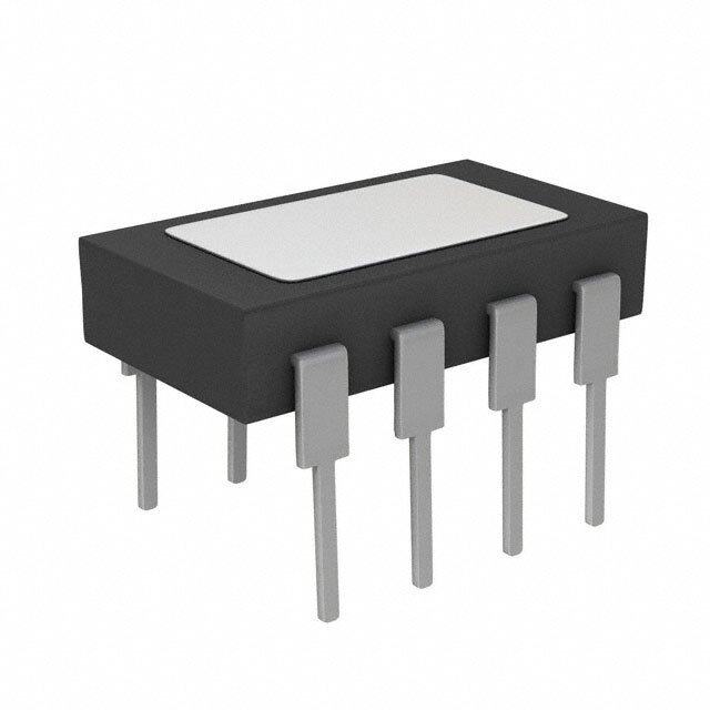
| 供应商器件封装 | 8-PDIP |
| 其它名称 | MCP2551IP |
| 包装 | 管件 |
| 协议 | CAN |
| 双工 | 半 |
| 商标 | Microchip Technology |
| 安装类型 | 通孔 |
| 安装风格 | Through Hole |
| 封装 | Tube |
| 封装/外壳 | 8-DIP(0.300",7.62mm) |
| 封装/箱体 | PDIP-8 |
| 工作温度 | -40°C ~ 85°C |
| 工作电源电压 | 5 V |
| 工厂包装数量 | 60 |
| 接收器滞后 | 200mV |
| 收发器数量 | 1 |
| 数据速率 | 1 Mbps |
| 最大工作温度 | + 85 C |
| 最小工作温度 | - 40 C |
| 标准包装 | 60 |
| 电压-电源 | 4.5 V ~ 5.5 V |
| 电源电压-最大 | 5.5 V |
| 电源电压-最小 | 4.5 V |
| 电源电流—最大值 | 75 mA |
| 类型 | 收发器 |
| 配用 | /product-detail/zh/AC164130-2/AC164130-2-ND/2651276/product-detail/zh/MCP2515DM-BM/MCP2515DM-BM-ND/1999510/product-detail/zh/MCP2515DM-PTPLS/MCP2515DM-PTPLS-ND/1999509/product-detail/zh/AC164130/AC164130-ND/1870542 |
| 驱动器/接收器数 | 1/1 |


- 商务部:美国ITC正式对集成电路等产品启动337调查
- 曝三星4nm工艺存在良率问题 高通将骁龙8 Gen1或转产台积电
- 太阳诱电将投资9.5亿元在常州建新厂生产MLCC 预计2023年完工
- 英特尔发布欧洲新工厂建设计划 深化IDM 2.0 战略
- 台积电先进制程称霸业界 有大客户加持明年业绩稳了
- 达到5530亿美元!SIA预计今年全球半导体销售额将创下新高
- 英特尔拟将自动驾驶子公司Mobileye上市 估值或超500亿美元
- 三星加码芯片和SET,合并消费电子和移动部门,撤换高东真等 CEO
- 三星电子宣布重大人事变动 还合并消费电子和移动部门
- 海关总署:前11个月进口集成电路产品价值2.52万亿元 增长14.8%


PDF Datasheet 数据手册内容提取
Not Recommended for New Designs Please use MCP2561 MCP2551 High-Speed CAN Transceiver Features Package Types • Supports 1 Mb/s operation PDIP/SOIC • Implements ISO-11898 standard physical layer requirements • Suitable for 12V and 24V systems TXD 1 8 RS • Externally-controlled slope for reduced RFI emissions VSS 2 1 7 CANH 5 5 • Detection of ground fault (permanent Dominant) 2 on TXD input VDD 3 CP 6 CANL • Power-on Reset and voltage brown-out protection M RXD 4 5 VREF • An unpowered node or brown-out event will not disturb the CAN bus • Low current standby operation • Protection against damage due to short-circuit conditions (positive or negative battery voltage) • Protection against high-voltage transients • Automatic thermal shutdown protection • Up to 112 nodes can be connected • High-noise immunity due to differential bus implementation • Temperature ranges: - Industrial (I): -40°C to +85°C - Extended (E): -40°C to +125°C Block Diagram VDD TXD Thermal Dominant Shutdown VDD Detect TXD Driver Control Slope Power-On CANH RS Control Reset 0.5VDD RXD GND CANL Receiver Reference VREF Voltage VSS 2001-2016 Microchip Technology Inc. DS20001667G-page 1
MCP2551 NOTES: DS20001667G-page 2 2001-2016 Microchip Technology Inc.
MCP2551 1.0 DEVICE OVERVIEW 1.4 Operating Modes The MCP2551 is a high-speed CAN, fault-tolerant The RS pin allows three modes of operation to be device that serves as the interface between a CAN selected: protocol controller and the physical bus. The MCP2551 • High-Speed device provides differential transmit and receive • Slope-Control capability for the CAN protocol controller, and is fully • Standby compatible with the ISO-11898 standard, including 24V requirements. It will operate at speeds of up to 1 Mb/s. These modes are summarized in Table 1-1. Typically, each node in a CAN system must have a When in High-Speed or Slope-Control mode, the device to convert the digital signals generated by a drivers for the CANH and CANL signals are internally CAN controller to signals suitable for transmission over regulated to provide controlled symmetry in order to the bus cabling (differential output). It also provides a minimize EMI emissions. buffer between the CAN controller and the high-voltage Additionally, the slope of the signal transitions on spikes that can be generated on the CAN bus by CANH and CANL can be controlled with a resistor outside sources (EMI, ESD, electrical transients, etc.). connected from pin 8 (RS) to ground. The slope must be proportional to the current output at RS, which will 1.1 Transmitter Function further reduce EMI emissions. The CAN bus has two states: Dominant and 1.4.1 HIGH-SPEED Recessive. A Dominant state occurs when the differential voltage between CANH and CANL is High-Speed mode is selected by connecting the RS pin greater than a defined voltage (e.g.,1.2V). A Recessive to VSS. In this mode, the transmitter output drivers have state occurs when the differential voltage is less than a fast output rise and fall times to support high-speed defined voltage (typically 0V). The Dominant and CAN bus rates. Recessive states correspond to the Low and High state 1.4.2 SLOPE-CONTROL of the TXD input pin, respectively. However, a Dominant state initiated by another CAN node will Slope-Control mode further reduces EMI by limiting the override a Recessive state on the CAN bus. rise and fall times of CANH and CANL. The slope, or slew rate (SR), is controlled by connecting an external 1.1.1 MAXIMUM NUMBER OF NODES resistor (REXT) between RS and VOL (usually ground). The MCP2551 CAN outputs will drive a minimum load The slope is proportional to the current output at the RS of 45, allowing a maximum of 112 nodes to be pin. Since the current is primarily determined by the connected (given a minimum differential input slope-control resistance value REXT, a certain slew rate resistance of 20 k and a nominal termination resistor is achieved by applying a specific resistance. value of 120 Figure 1-1 illustrates typical slew rate values as a function of the slope-control resistance value. 1.2 Receiver Function 1.4.3 STANDBY MODE The RXD output pin reflects the differential bus voltage The device may be placed in Standby or SLEEP mode between CANH and CANL. The Low and High states of by applying a high-level to the RS pin. In SLEEP mode, the RXD output pin correspond to the Dominant and the transmitter is switched off and the receiver operates Recessive states of the CAN bus, respectively. at a lower current. The receive pin on the controller side (RXD) is still functional, but will operate at a slower 1.3 Internal Protection rate. The attached microcontroller can monitor RXD for CAN bus activity and place the transceiver into normal CANH and CANL are protected against battery short operation via the RS pin (at higher bus rates, the first circuits and electrical transients that can occur on the CAN message may be lost). CAN bus. This feature prevents destruction of the transmitter output stage during such a fault condition. The device is further protected from excessive current loading by thermal shutdown circuitry that disables the output drivers when the junction temperature exceeds a nominal limit of 165°C. All other parts of the chip remain operational, and the chip temperature is low- ered due to the decreased power dissipation in the transmitter outputs. This protection is essential to protect against bus line short-circuit-induced damage. 2001-2016 Microchip Technology Inc. DS20001667G-page 3
MCP2551 TABLE 1-1: MODES OF OPERATION Mode Current at Rs Pin Resulting Voltage at RS Pin Standby -IRS < 10 µA VRS > 0.75 VDD Slope-Control 10 µA < -IRS < 200 µA 0.4 VDD < VRS < 0.6 VDD High-Speed -IRS < 610 µA 0 < VRS < 0.3VDD TABLE 1-2: TRANSCEIVER TRUTH TABLE VDD VRS TXD CANH CANL Bus State( 1) RXD( 1) 0 HIGH LOW Dominant 0 VRS < 0.75 VDD 4.5V VDD 5.5V 1 or floating Not Driven Not Driven Recessive 1 VRS > 0.75 VDD X Not Driven Not Driven Recessive 1 0 HIGH LOW Dominant 0 VPOR < VDD < 4.5V VRS < 0.75 VDD 1 or floating Not Driven Not Driven Recessive 1 (See Note 3) VRS > 0.75 VDD X Not Driven Not Driven Recessive 1 Not Driven/ Not Driven/ 0 < VDD < VPOR X X High Impedance X No Load No Load Note 1: If another bus node is transmitting a Dominant bit on the CAN bus, then RXD is a logic ‘0’. 2: X = “don’t care”. 3: Device drivers will function, although outputs are not ensured to meet the ISO-11898 specification. FIGURE 1-1: SLEW RATE VS. SLOPE-CONTROL RESISTANCE VALUE 25 20 s μ V/ 15 e t a R 10 w e l S 5 0 10 20 30 40 49 60 70 76 90 100 110 120 Resistance (k ) (cid:159) DS20001667G-page 4 2001-2016 Microchip Technology Inc.
MCP2551 1.5 TXD Permanent Dominant 1.7.1 TRANSMITTER DATA INPUT (TXD) Detection TXD is a TTL-compatible input pin. The data on this pin is driven out on the CANH and CANL differential output If the MCP2551 detects an extended Low state on the pins. It is usually connected to the transmitter data TXD input, it will disable the CANH and CANL output output of the CAN controller device. When TXD is low, drivers in order to prevent the corruption of data on the CANH and CANL are in the Dominant state. When TXD CAN bus. The drivers are disabled if TXD is Low for is high, CANH and CANL are in the Recessive state, more than 1.25 ms (minimum). This implies a provided that another CAN node is not driving the CAN maximum bit time of 62.5 µs (16 kb/s bus rate), bus with a Dominant state. TXD has an internal pull-up allowing up to 20 consecutive transmitted Dominant resistor (nominal 25 k to VDD). bits during a multiple bit error and error frame scenario. The drivers remain disabled as long as TXD remains 1.7.2 GROUND SUPPLY (VSS) Low. A rising edge on TXD will reset the timer logic and enable the CANH and CANL output drivers. Ground supply pin. 1.7.3 SUPPLY VOLTAGE (V ) 1.6 Power-on Reset DD Positive supply voltage pin. When the device is powered on, CANH and CANL remain in a high-impedance state until VDD reaches the 1.7.4 RECEIVER DATA OUTPUT (RXD) voltage level VPORH. In addition, CANH and CANL will RXD is a CMOS-compatible output that drives high or remain in a high-impedance state if TXD is Low when low depending on the differential signals on the CANH VDD reaches VPORH. CANH and CANL will become and CANL pins and is usually connected to the receiver active only after TXD is asserted High. Once powered data input of the CAN controller device. RXD is High on, CANH and CANL will enter a high-impedance state when the CAN bus is Recessive and Low in the if the voltage level at VDD falls below VPORL, providing Dominant state. voltage brown-out protection during normal operation. 1.7.5 REFERENCE VOLTAGE (VREF) 1.7 Pin Descriptions Reference Voltage Output (defined as VDD/2). The 8-pin pinout is listed in Table 1-3. 1.7.6 CAN LOW (CANL) TABLE 1-3: MCP2551 PINOUT The CANL output drives the low side of the CAN differential bus. This pin is also tied internally to the Pin Pin Pin Function receive input comparator. Number Name 1 TXD Transmit Data Input 1.7.7 CAN HIGH (CANH) 2 VSS Ground The CANH output drives the high side of the CAN 3 VDD Supply Voltage differential bus. This pin is also tied internally to the receive input comparator. 4 RXD Receive Data Output 5 VREF Reference Output Voltage 1.7.8 SLOPE RESISTOR INPUT (RS) 6 CANL CAN Low-Level Voltage I/O The RS pin is used to select High-Speed, Slope-Control 7 CANH CAN High-Level Voltage I/O or Standby modes via an external biasing resistor. 8 RS Slope-Control Input 2001-2016 Microchip Technology Inc. DS20001667G-page 5
MCP2551 NOTES: DS20001667G-page 6 2001-2016 Microchip Technology Inc.
MCP2551 2.0 ELECTRICAL 2.1.5 DIFFERENTIAL VOLTAGE, VDIFF CHARACTERISTICS (OF CAN BUS) Differential voltage of the two-wire CAN bus, value 2.1 Terms and Definitions VDIFF = VCANH – VCANL. A number of terms are defined in ISO-11898 that are 2.1.6 INTERNAL CAPACITANCE, CIN used to describe the electrical characteristics of a CAN (OF A CAN NODE) transceiver device. These terms and definitions are Capacitance seen between CANL (or CANH) and summarized in this section. ground during the Recessive state when the CAN node 2.1.1 BUS VOLTAGE is disconnected from the bus (see Figure 2-1). VCANL and VCANH denote the voltages of the bus line 2.1.7 INTERNAL RESISTANCE, RIN wires CANL and CANH relative to ground of each (OF A CAN NODE) individual CAN node. Resistance seen between CANL (or CANH) and 2.1.2 COMMON MODE BUS VOLTAGE ground during the Recessive state when the CAN node RANGE is disconnected from the bus (see Figure 2-1). Boundary voltage levels of VCANL and VCANH with FIGURE 2-1: PHYSICAL LAYER respect to ground, for which proper operation will occur, DEFINITIONS if up to the maximum number of CAN nodes are connected to the bus. ECU 2.1.3 DIFFERENTIAL INTERNAL CAPACITANCE, CDIFF RIN (OF A CAN NODE) CANL Capacitance seen between CANL and CANH during RDIFF CDIFF the Recessive state when the CAN node is RIN disconnected from the bus (see Figure 2-1). CANH CIN CIN 2.1.4 DIFFERENTIAL INTERNAL GROUND RESISTANCE, RDIFF (OF A CAN NODE) Resistance seen between CANL and CANH during the Recessive state when the CAN node is disconnected from the bus (see Figure 2-1). 2001-2016 Microchip Technology Inc. DS20001667G-page 7
MCP2551 Absolute Maximum Ratings† VDD.............................................................................................................................................................................7.0V DC Voltage at TXD, RXD, VREF and VS............................................................................................-0.3V to VDD + 0.3V DC Voltage at CANH, CANL (Note 1)..........................................................................................................-42V to +42V Transient Voltage on Pins 6 and 7 (Note 2).............................................................................................-250V to +250V Storage temperature...............................................................................................................................-55°C to +150°C Operating ambient temperature..............................................................................................................-40°C to +125°C Virtual Junction Temperature, TVJ (Note 3).............................................................................................-40°C to +150°C Soldering temperature of leads (10 seconds).......................................................................................................+300°C ESD protection on CANH and CANL pins (Note 4)...................................................................................................6 kV ESD protection on all other pins (Note 4)..................................................................................................................4 kV Note1:Short-circuit applied when TXD is High and Low. 2: In accordance with ISO-7637. 3: In accordance with IEC 60747-1. 4: Classification A: Human Body Model. † NOTICE: Stresses above those listed under “Maximum ratings” may cause permanent damage to the device. This is a stress rating only and functional operation of the device at those or any other conditions above those indicated in the operational listings of this specification is not implied. Exposure to maximum rating conditions for extended periods may affect device reliability. DS20001667G-page 8 2001-2016 Microchip Technology Inc.
MCP2551 2.2 DC Characteristics Electrical Characteristics: DC Specifications Industrial (I): TAMB = -40°C to +85°C VDD = 4.5V to 5.5V Extended (E): TAMB = -40°C to +125°CVDD = 4.5V to 5.5V Param Sym Characteristic Min Max Units Conditions No. Supply D1 — 75 mA Dominant; VTXD = 0.8V; VDD Recessive; VTXD = +2V; D2 — 10 mA RS = 47 kW IDD Supply Current -40°C T +85°C, Standby; — 365 µA AMB (Note 2) D3 -40°C T +125°C, — 465 µA AMB Standby; (Note 2) High-level of the Power-on CANH, CANL outputs are active D4 VPORH 3.8 4.3 V Reset comparator when VDD > VPORH Low-level of the Power-on CANH, CANL outputs are not D5 VPORL 3.4 4.0 V Reset comparator active when VDD < VPORL Hysteresis of Power-on D6 VPORD 0.3 0.8 V Note 1 Reset comparator Bus Line (CANH; CANL) Transmitter D7 VVCCAANNHL((rr)); CbuAsN vHo,l tCagAeNL Recessive 2.0 3.0 V VTXD = VDD; no load. -2V < V(CAHL,CANH) < +7V, D8 -2 +2 mA IO(CANH)(reces) 0V <VDD < 5.5V Recessive output current IO(CANL)(reces) -5V < V(CANL,CANH) < +40V, D9 -10 +10 mA 0V <VDD < 5.5V CANH Dominant D10 VO(CANH) 2.75 4.5 V VTXD = 0.8V output voltage CANL Dominant D11 VO(CANL) 0.5 2.25 V VTXD = 0.8V output voltage Recessive differential D12 VDIFF(r)(o) -500 +50 mV VTXD = 2V; no load output voltage Dominant differential VTXD = 0.8V; VDD = 5V D13 VDIFF(d)(o) 1.5 3.0 V output voltage 40W < RL < 60W (Note 2) D14 — -200 mA VCANH = -5V CANH short-circuit IO(SC)(CANH) -100 D15 output current — mA VCANH = -40V, +40V. (Note 1) (typical) CANL short-circuit D16 IO(SC)(CANL)l — 200 mA VCANL = -40V, +40V. (Note 1) output current -2V < V(CANL, CANH) < +7V -1.0 +0.5 V Recessive differential (Note 3) D17 VDIFF(r)(i) input voltage -12V < V(CANL, CANH) < +12V -1.0 +0.4 V (Note 3) Note 1: This parameter is periodically sampled and not 100% tested. 2: ITXD = IRXD = IVREF = 0 mA; 0V < VCANL < VDD; 0V < VCANH < VDD; VRS = VDD. 3: This is valid for the receiver in all modes; High-speed, Slope-control and Standby. 2001-2016 Microchip Technology Inc. DS20001667G-page 9
MCP2551 2.2 DC Characteristics (Continued) Electrical Characteristics: DC Specifications (Continued) Industrial (I): TAMB = -40°C to +85°C VDD = 4.5V to 5.5V Extended (E): TAMB = -40°C to +125°CVDD = 4.5V to 5.5V Param Sym Characteristic Min Max Units Conditions No. Bus Line (CANH; CANL) Receiver: [TXD = 2V; pins 6 and 7 externally driven] -2V < V(CANL, CANH) < +7V 0.9 5.0 V Dominant differential (Note 3) D18 VDIFF(d)(i) input voltage -12V < V(CANL, CANH) < +12V 1.0 5.0 V (Note 3) D19 VDIFF(h)(i) Differential input hysteresis 100 200 mV See Figure 2-3 (Note 1) CANH, CANL Common- D20 RIN 5 50 kW mode input resistance Deviation between CANH D21 RIN(d) and CANL Common-mode -3 +3 % VCANH = VCANL input resistance Bus Line (CANH; CANL) Receiver: [TXD = 2V; pins 6 and 7 externally driven] D22 RDIFF Differential input resistance 20 100 kW CANH, CANL input leakage VDD < VPOR; D24 ILI — 150 µA current VCANH = VCANL = +5V Transmitter Data Input (TXD) D25 VIH High-level input voltage 2.0 VDD V Output Recessive D26 VIL Low-level input voltage VSS +0.8 V Output Dominant D27 IIH High-level input current -1 +1 µA VTXD = VDD D28 IIL Low-level input current -100 -400 µA VTXD = 0V Receiver Data Output (RXD) 0.7 VD D31 VOH High-level output voltage — V IOH = 8 mA D D32 VOL Low-level output voltage — 0.8 V IOL = 8 mA Voltage Reference Output (VREF) 0.45 V 0.55 VD D33 VREF Reference output voltage V -50 µA < IVREF < 50 µA DD D Standby/Slope-Control (RS pin) Input voltage for standby 0.75 V D34 VSTB — V mode DD D35 ISLOPE Slope-control mode current -10 -200 µA 0.4 VD D36 VSLOPE Slope-control mode voltage 0.6 VDD V D Thermal Shutdown Shutdown junction D37 TJ(sd) temperature 155 180 oC Note 1 Shutdown temperature -12V < V(CANL, CANH) < +12V D38 TJ(h) hysteresis 20 30 oC (Note 3) Note 1: This parameter is periodically sampled and not 100% tested. 2: ITXD = IRXD = IVREF = 0 mA; 0V < VCANL < VDD; 0V < VCANH < VDD; VRS = VDD. 3: This is valid for the receiver in all modes; High-speed, Slope-control and Standby. DS20001667G-page 10 2001-2016 Microchip Technology Inc.
MCP2551 FIGURE 2-1: TEST CIRCUIT FOR ELECTRICAL CHARACTERISTICS 0.1µF V DD CANH TXD VREF CAN 60 100pF Transceiver RXD CANL 30pF GND RS Rext Note: RS may be connected to VDD or GND via a load resistor depending on desired operating mode as described in Section 1.7.3 “Supply Voltage (V )”. DD FIGURE 2-2: TEST CIRCUIT FOR AUTOMOTIVE TRANSIENTS 500pF CANH TXD Schaffner VREF CAN 60 Generator Transceiver RXD CANL 500pF GND RS Note: RS may be connected to VDD or Rext GND via a load resistor depending on desired operating mode as described in Section 1.7.8 “Slope Resistor Input (Rs)”. The wave forms of the applied transients shall be in accordance with “ISO-7637, Part 1”, test pulses 1, 2, 3a and 3b. FIGURE 2-3: HYSTERESIS OF THE RECEIVER RXD (receive data VOH output voltage) VDIFF (r)(i) VDIFF (d)(i) VOL hysteresis D19 0.5 0.9 VDIFF (V) 2001-2016 Microchip Technology Inc. DS20001667G-page 11
MCP2551 2.3 AC Characteristics Electrical Characteristics: AC Specifications Industrial (I): TAMB = -40°C to +85°C VDD = 4.5V to 5.5V Extended (E): TAMB = -40°C to +125°CVDD = 4.5V to 5.5V Param Sym Characteristic Min Max Units Conditions No. 1 tBIT Bit time 1 62.5 µs VRS = 0V 2 fBIT Bit frequency 16 1000 kHz VRS = 0V -40°C TAMB +125°C, 3 TtxL2bus(d) Delay TXD to bus active — 70 ns VRS = 0V -40°C TAMB +85°C, — 125 ns VRS = 0V 4 TtxH2bus(r) Delay TXD to bus inactive -40°C TAMB +125°C, — 170 ns VRS = 0V -40°C TAMB +125°C, — 130 ns VRS = 0V 5 TtxL2rx(d) Delay TXD to receive active -40°C TAMB +125°C, — 250 ns RS = 47 k -40°C TAMB +85°C, — 175 ns VRS = 0V -40°C TAMB +85°C, — 225 ns Delay TXD to receiver RS = 47 k 6 TtxH2rx(r) inactive -40°C TAMB +125°C, — 235 ns VRS = 0V -40°C TAMB +125°C, — 400 ns RS = 47 k Refer to Figure 2-1; 7 SR CANH, CANL slew rate 5.5 8.5 V/µs RS = 47 kNote 1) Wake-up time from standby 10 tWAKE — 5 µs See Figure 2-5 (Rs pin) Bus Dominant to RXD Low 11 TbusD2rx(s) — 550 ns VRS = +4V; (See Figure 2-6) (Standby mode) CIN(CANH) CANH; CANL input 20 1 Mb/s data rate; 12 — pF CIN(CANL) capacitance (typical) VTXD = VDD, (Note 1) Differential input 10 1 Mb/s data rate 13 CDIFF — pF capacitance (typical) (Note 1) TX Permanent Dominant 14 TtxL2busZ 1.25 4 ms Timer Disable Time Rising edge on TXD while TX Permanent Dominant 15 TtxR2pdt(res) — 1 µs device is in permanent Timer Reset Time Dominant state Note1: This parameter is periodically sampled and not 100% tested. DS20001667G-page 12 2001-2016 Microchip Technology Inc.
MCP2551 2.4 Timing Diagrams and Specifications FIGURE 2-4: TIMING DIAGRAM FOR AC CHARACTERISTICS VDD TXD (transmit data input voltage) 0V VDIFF (CANH, CANL differential 0.9V 0.5V voltage) RXD (receive data 0.3VDD 0.7VDD output voltage) 3 5 4 6 FIGURE 2-5: TIMING DIAGRAM FOR WAKE-UP FROM STANDBY VRS Slope resistor VDD input voltage 0.6VDD 0V VRXD Receive data output voltage 0.3VDD 10 VTXD = 0.8V FIGURE 2-6: TIMING DIAGRAM FOR BUS DOMINANT TO RXD LOW (STANDBY MODE) 1.5V VDIFF, Differential 0.9V voltage 0V Receive data output voltage 0.3VDD 11 VRS = 4V; VTXD = 2V 2001-2016 Microchip Technology Inc. DS20001667G-page 13
MCP2551 NOTES: DS20001667G-page 14 2001-2016 Microchip Technology Inc.
MCP2551 3.0 PACKAGING INFORMATION 3.1 Package Marking Information 8-Lead PDIP (300 mil) Example: MCP2551 E/P^e^3^256 1642 8-Lead SOIC (150 mil) Example: MCP2551E SN^e^3^1642 256 NNN Legend: XX...X Customer-specific information Y Year code (last digit of calendar year) YY Year code (last 2 digits of calendar year) WW Week code (week of January 1 is week ‘01’) NNN Alphanumeric traceability code e3 Pb-free JEDEC® designator for Matte Tin (Sn) * This package is Pb-free. The Pb-free JEDEC designator ( e 3 ) can be found on the outer packaging for this package. Note: In the event the full Microchip part number cannot be marked on one line, it will be carried over to the next line, thus limiting the number of available characters for customer-specific information. 2001-2016 Microchip Technology Inc. DS20001667G-page 15
MCP2551 8-Lead Plastic Dual In-Line (P) - 300 mil Body [PDIP] Note: For the most current package drawings, please see the Microchip Packaging Specification located at http://www.microchip.com/packaging D A N B E1 NOTE 1 1 2 TOP VIEW E C A A2 PLANE L c A1 e eB 8X b1 8X b .010 C SIDE VIEW END VIEW Microchip Technology Drawing No. C04-018D Sheet 1 of 2 DS20001667G-page 16 2001-2016 Microchip Technology Inc.
MCP2551 8-Lead Plastic Dual In-Line (P) - 300 mil Body [PDIP] Note: For the most current package drawings, please see the Microchip Packaging Specification located at http://www.microchip.com/packaging ALTERNATE LEAD DESIGN (VENDOR DEPENDENT) DATUM A DATUM A b b e e 2 2 e e Units INCHES Dimension Limits MIN NOM MAX Number of Pins N 8 Pitch e .100 BSC Top to Seating Plane A - - .210 Molded Package Thickness A2 .115 .130 .195 Base to Seating Plane A1 .015 - - Shoulder to Shoulder Width E .290 .310 .325 Molded Package Width E1 .240 .250 .280 Overall Length D .348 .365 .400 Tip to Seating Plane L .115 .130 .150 Lead Thickness c .008 .010 .015 Upper Lead Width b1 .040 .060 .070 Lower Lead Width b .014 .018 .022 Overall Row Spacing § eB - - .430 Notes: 1. Pin 1 visual index feature may vary, but must be located within the hatched area. 2. § Significant Characteristic 3. Dimensions D and E1 do not include mold flash or protrusions. Mold flash or protrusions shall not exceed .010" per side. 4. Dimensioning and tolerancing per ASME Y14.5M BSC: Basic Dimension. Theoretically exact value shown without tolerances. Microchip Technology Drawing No. C04-018D Sheet 2 of 2 2001-2016 Microchip Technology Inc. DS20001667G-page 17
MCP2551 Note: For the most current package drawings, please see the Microchip Packaging Specification located at http://www.microchip.com/packaging DS20001667G-page 18 2001-2016 Microchip Technology Inc.
MCP2551 Note: For the most current package drawings, please see the Microchip Packaging Specification located at http://www.microchip.com/packaging 2001-2016 Microchip Technology Inc. DS20001667G-page 19
MCP2551 (cid:2)(cid:3)(cid:4)(cid:5)(cid:6)(cid:7)(cid:8)(cid:9)(cid:10)(cid:6)(cid:11)(cid:12)(cid:13)(cid:14)(cid:8)(cid:15)(cid:16)(cid:6)(cid:10)(cid:10)(cid:8)(cid:17)(cid:18)(cid:12)(cid:10)(cid:13)(cid:19)(cid:5)(cid:8)(cid:20)(cid:15)(cid:21)(cid:22)(cid:8)(cid:23)(cid:8)(cid:21)(cid:6)(cid:24)(cid:24)(cid:25)(cid:26)(cid:27)(cid:8)(cid:28)(cid:29)(cid:30)(cid:31)(cid:8)(cid:16)(cid:16)(cid:8) (cid:25)(cid:7)!(cid:8)"(cid:15)(cid:17)#$% (cid:21)(cid:25)(cid:12)(cid:5)& (cid:30)(cid:10)(cid:9)(cid:2)(cid:31)(cid:11)(cid:14)(cid:2)!(cid:10)"(cid:31)(cid:2)(cid:8)#(cid:9)(cid:9)(cid:14)(cid:15)(cid:31)(cid:2)(cid:12)(cid:28)(cid:8)$(cid:28)(cid:17)(cid:14)(cid:2)%(cid:9)(cid:28)&(cid:7)(cid:15)(cid:17)"’(cid:2)(cid:12)(cid:16)(cid:14)(cid:28)"(cid:14)(cid:2)"(cid:14)(cid:14)(cid:2)(cid:31)(cid:11)(cid:14)(cid:2)(cid:6)(cid:7)(cid:8)(cid:9)(cid:10)(cid:8)(cid:11)(cid:7)(cid:12)(cid:2)((cid:28)(cid:8)$(cid:28)(cid:17)(cid:7)(cid:15)(cid:17)(cid:2)(cid:22)(cid:12)(cid:14)(cid:8)(cid:7))(cid:7)(cid:8)(cid:28)(cid:31)(cid:7)(cid:10)(cid:15)(cid:2)(cid:16)(cid:10)(cid:8)(cid:28)(cid:31)(cid:14)%(cid:2)(cid:28)(cid:31)(cid:2) (cid:11)(cid:31)(cid:31)(cid:12)*++&&&(cid:20)!(cid:7)(cid:8)(cid:9)(cid:10)(cid:8)(cid:11)(cid:7)(cid:12)(cid:20)(cid:8)(cid:10)!+(cid:12)(cid:28)(cid:8)$(cid:28)(cid:17)(cid:7)(cid:15)(cid:17) DS20001667G-page 20 2001-2016 Microchip Technology Inc.
MCP2551 APPENDIX A: REVISION HISTORY Revision G (December 2016) The following is the list of modifications: • Added note to page 1 header: “Not recommended for new designs”. • Updated Section 3.1 “Package Marking Infor- mation”. • Minor typographical corrections. Revision F (July 2010) The following is the list of modifications: • Updates to the packaging diagrams. Revision E (January 2007) The following is the list of modifications: • Updates to the packaging diagrams. Revision A (June 2001) • Original Release of this Document. 2001-2016 Microchip Technology Inc. DS20001667G-page 21
MCP2551 NOTES: DS20001667G-page 22 2001-2016 Microchip Technology Inc.
MCP2551 PRODUCT IDENTIFICATION SYSTEM To order or obtain information, e.g., on pricing or delivery, refer to the factory or the listed sales office. PART NO. -X /XX XXX Examples: Device Temperature Package Pattern a) MCP2551-I/P: Industrial temperature, Range PDIP package. b) MCP2551-E/P: Extended temperature, PDIP package. Device: MCP2551: High-Speed CAN Transceiver c) MCP2551-I/SN: Industrial temperature, MCP2551T: High-Speed CAN Transceiver SOIC package. (Tape and Reel) d) MCP2551T-I/SN: Tape and Reel, Industrial Temperature, Temperature I = -40°C to +85°C SOIC package. Range: E = -40°C to +125°C e) MCP2551T-E/SN:Tape and Reel, Extended Temperature, SOIC package. Package: P = Plastic DIP (300 mil Body) 8-lead SN = Plastic SOIC (150 mil Body) 8-lead f) MCP2551-E/SN: Extended Temperature, SOIC package. 2001-2016 Microchip Technology Inc. DS20001667G-page 23
MCP2551 NOTES: DS20001667G-page 24 2001-2016 Microchip Technology Inc.
Note the following details of the code protection feature on Microchip devices: • Microchip products meet the specification contained in their particular Microchip Data Sheet. • Microchip believes that its family of products is one of the most secure families of its kind on the market today, when used in the intended manner and under normal conditions. • There are dishonest and possibly illegal methods used to breach the code protection feature. All of these methods, to our knowledge, require using the Microchip products in a manner outside the operating specifications contained in Microchip’s Data Sheets. Most likely, the person doing so is engaged in theft of intellectual property. • Microchip is willing to work with the customer who is concerned about the integrity of their code. • Neither Microchip nor any other semiconductor manufacturer can guarantee the security of their code. Code protection does not mean that we are guaranteeing the product as “unbreakable.” Code protection is constantly evolving. We at Microchip are committed to continuously improving the code protection features of our products. Attempts to break Microchip’s code protection feature may be a violation of the Digital Millennium Copyright Act. If such acts allow unauthorized access to your software or other copyrighted work, you may have a right to sue for relief under that Act. Information contained in this publication regarding device Trademarks applications and the like is provided only for your convenience The Microchip name and logo, the Microchip logo, AnyRate, AVR, and may be superseded by updates. It is your responsibility to AVR logo, AVR Freaks, BeaconThings, BitCloud, CryptoMemory, ensure that your application meets with your specifications. CryptoRF, dsPIC, FlashFlex, flexPWR, Heldo, JukeBlox, KEELOQ, MICROCHIP MAKES NO REPRESENTATIONS OR KEELOQ logo, Kleer, LANCheck, LINK MD, maXStylus, WARRANTIES OF ANY KIND WHETHER EXPRESS OR maXTouch, MediaLB, megaAVR, MOST, MOST logo, MPLAB, IMPLIED, WRITTEN OR ORAL, STATUTORY OR OptoLyzer, PIC, picoPower, PICSTART, PIC32 logo, Prochip OTHERWISE, RELATED TO THE INFORMATION, Designer, QTouch, RightTouch, SAM-BA, SpyNIC, SST, SST INCLUDING BUT NOT LIMITED TO ITS CONDITION, Logo, SuperFlash, tinyAVR, UNI/O, and XMEGA are registered QUALITY, PERFORMANCE, MERCHANTABILITY OR trademarks of Microchip Technology Incorporated in the U.S.A. FITNESS FOR PURPOSE. Microchip disclaims all liability and other countries. arising from this information and its use. Use of Microchip ClockWorks, The Embedded Control Solutions Company, devices in life support and/or safety applications is entirely at EtherSynch, Hyper Speed Control, HyperLight Load, IntelliMOS, the buyer’s risk, and the buyer agrees to defend, indemnify and mTouch, Precision Edge, and Quiet-Wire are registered hold harmless Microchip from any and all damages, claims, trademarks of Microchip Technology Incorporated in the U.S.A. suits, or expenses resulting from such use. No licenses are Adjacent Key Suppression, AKS, Analog-for-the-Digital Age, Any conveyed, implicitly or otherwise, under any Microchip Capacitor, AnyIn, AnyOut, BodyCom, chipKIT, chipKIT logo, intellectual property rights unless otherwise stated. CodeGuard, CryptoAuthentication, CryptoCompanion, CryptoController, dsPICDEM, dsPICDEM.net, Dynamic Average Matching, DAM, ECAN, EtherGREEN, In-Circuit Serial Programming, ICSP, Inter-Chip Connectivity, JitterBlocker, KleerNet, KleerNet logo, Mindi, MiWi, motorBench, MPASM, MPF, MPLAB Certified logo, MPLIB, MPLINK, MultiTRAK, NetDetach, Omniscient Code Generation, PICDEM, PICDEM.net, PICkit, PICtail, PureSilicon, QMatrix, RightTouch logo, REAL ICE, Ripple Blocker, SAM-ICE, Serial Quad I/O, SMART-I.S., SQI, SuperSwitcher, SuperSwitcher II, Total Endurance, TSHARC, USBCheck, VariSense, ViewSpan, WiperLock, Wireless DNA, and ZENA are trademarks of Microchip Technology Incorporated in the U.S.A. and other countries. SQTP is a service mark of Microchip Technology Incorporated in Microchip received ISO/TS-16949:2009 certification for its worldwide the U.S.A. headquarters, design and wafer fabrication facilities in Chandler and Tempe, Arizona; Gresham, Oregon and design centers in California Silicon Storage Technology is a registered trademark of Microchip and India. The Company’s quality system processes and procedures Technology Inc. in other countries. are for its PIC® MCUs and dsPIC® DSCs, KEELOQ® code hopping devices, Serial EEPROMs, microperipherals, nonvolatile memory and GestIC is a registered trademark of Microchip Technology analog products. In addition, Microchip’s quality system for the design Germany II GmbH & Co. KG, a subsidiary of Microchip Technology and manufacture of development systems is ISO 9001:2000 certified. Inc., in other countries. All other trademarks mentioned herein are property of their QUALITY MANAGEMENT SYSTEM respective companies. © 2001-2016, Microchip Technology Incorporated, All Rights CERTIFIED BY DNV Reserved. ISBN: 978-1-5224-1198-7 == ISO/TS 16949 == 2001-2016 Microchip Technology Inc. DS20001667G-page 25
Worldwide Sales and Service AMERICAS ASIA/PACIFIC ASIA/PACIFIC EUROPE Corporate Office Asia Pacific Office China - Xiamen Austria - Wels 2355 West Chandler Blvd. Suites 3707-14, 37th Floor Tel: 86-592-2388138 Tel: 43-7242-2244-39 Chandler, AZ 85224-6199 Tower 6, The Gateway Fax: 86-592-2388130 Fax: 43-7242-2244-393 Tel: 480-792-7200 Harbour City, Kowloon China - Zhuhai Denmark - Copenhagen Fax: 480-792-7277 Hong Kong Tel: 86-756-3210040 Tel: 45-4450-2828 Technical Support: Tel: 852-2943-5100 Fax: 86-756-3210049 Fax: 45-4485-2829 http://www.microchip.com/ Fax: 852-2401-3431 India - Bangalore Finland - Espoo support Australia - Sydney Tel: 91-80-3090-4444 Tel: 358-9-4520-820 Web Address: www.microchip.com Tel: 61-2-9868-6733 Fax: 91-80-3090-4123 France - Paris Fax: 61-2-9868-6755 India - New Delhi Tel: 33-1-69-53-63-20 Atlanta China - Beijing Tel: 91-11-4160-8631 Fax: 33-1-69-30-90-79 Duluth, GA Tel: 678-957-9614 Tel: 86-10-8569-7000 Fax: 91-11-4160-8632 France - Saint Cloud Fax: 678-957-1455 Fax: 86-10-8528-2104 India - Pune Tel: 33-1-30-60-70-00 China - Chengdu Tel: 91-20-3019-1500 Germany - Garching ATeul:s 5ti1n2, -T2X57-3370 Tel: 86-28-8665-5511 Japan - Osaka Tel: 49-8931-9700 Fax: 86-28-8665-7889 Tel: 81-6-6152-7160 Germany - Haan Boston China - Chongqing Fax: 81-6-6152-9310 Tel: 49-2129-3766400 Westborough, MA Tel: 774-760-0087 Tel: 86-23-8980-9588 Japan - Tokyo Germany - Heilbronn Fax: 86-23-8980-9500 Tel: 81-3-6880- 3770 Tel: 49-7131-67-3636 Fax: 774-760-0088 China - Dongguan Fax: 81-3-6880-3771 Germany - Karlsruhe CItahsiccaa,g IoL Tel: 86-769-8702-9880 Korea - Daegu Tel: 49-721-625370 Tel: 630-285-0071 China - Guangzhou Tel: 82-53-744-4301 Germany - Munich Fax: 630-285-0075 Tel: 86-20-8755-8029 Fax: 82-53-744-4302 Tel: 49-89-627-144-0 China - Hangzhou Korea - Seoul Fax: 49-89-627-144-44 Dallas Addison, TX Tel: 86-571-8792-8115 Tel: 82-2-554-7200 Germany - Rosenheim Tel: 972-818-7423 Fax: 86-571-8792-8116 Fax: 82-2-558-5932 or Tel: 49-8031-354-560 Fax: 972-818-2924 China - Hong Kong SAR 82-2-558-5934 Israel - Ra’anana Detroit Tel: 852-2943-5100 Malaysia - Kuala Lumpur Tel: 972-9-744-7705 Fax: 852-2401-3431 Tel: 60-3-6201-9857 Novi, MI Italy - Milan Tel: 248-848-4000 China - Nanjing Fax: 60-3-6201-9859 Tel: 39-0331-742611 Houston, TX Tel: 86-25-8473-2460 Malaysia - Penang Fax: 39-0331-466781 Fax: 86-25-8473-2470 Tel: 60-4-227-8870 Tel: 281-894-5983 Italy - Padova Indianapolis China - Qingdao Fax: 60-4-227-4068 Tel: 39-049-7625286 Noblesville, IN Tel: 86-532-8502-7355 Philippines - Manila Netherlands - Drunen Fax: 86-532-8502-7205 Tel: 63-2-634-9065 Tel: 317-773-8323 Tel: 31-416-690399 Fax: 317-773-5453 China - Shanghai Fax: 63-2-634-9069 Fax: 31-416-690340 Tel: 317-536-2380 Tel: 86-21-3326-8000 Singapore Norway - Trondheim Fax: 86-21-3326-8021 Tel: 65-6334-8870 Los Angeles Tel: 47-7289-7561 Mission Viejo, CA China - Shenyang Fax: 65-6334-8850 Poland - Warsaw Tel: 949-462-9523 Tel: 86-24-2334-2829 Taiwan - Hsin Chu Tel: 48-22-3325737 Fax: 949-462-9608 Fax: 86-24-2334-2393 Tel: 886-3-5778-366 Tel: 951-273-7800 China - Shenzhen Fax: 886-3-5770-955 Romania - Bucharest Tel: 40-21-407-87-50 Raleigh, NC Tel: 86-755-8864-2200 Taiwan - Kaohsiung Tel: 919-844-7510 Fax: 86-755-8203-1760 Tel: 886-7-213-7830 Spain - Madrid Tel: 34-91-708-08-90 New York, NY China - Wuhan Taiwan - Taipei Fax: 34-91-708-08-91 Tel: 631-435-6000 Tel: 86-27-5980-5300 Tel: 886-2-2508-8600 Fax: 86-27-5980-5118 Fax: 886-2-2508-0102 Sweden - Gothenberg San Jose, CA Tel: 46-31-704-60-40 Tel: 408-735-9110 China - Xian Thailand - Bangkok Tel: 408-436-4270 Tel: 86-29-8833-7252 Tel: 66-2-694-1351 Sweden - Stockholm Fax: 86-29-8833-7256 Fax: 66-2-694-1350 Tel: 46-8-5090-4654 Canada - Toronto Tel: 905-695-1980 UK - Wokingham Fax: 905-695-2078 Tel: 44-118-921-5800 Fax: 44-118-921-5820 DS20001667G-page 26 2001-2016 Microchip Technology Inc. 11/07/16
Mouser Electronics Authorized Distributor Click to View Pricing, Inventory, Delivery & Lifecycle Information: M icrochip: MCP2551-E/SN MCP2551-I/SN MCP2551T-I/SN MCP2551-E/P MCP2551T-E/SN MCP2551-I/P MCP2551A-E/P MCP2551A-E/SN MCP2551A-I/P MCP2551A-I/SN MCP2551AT-E/SN MCP2551AT-I/SN