
 Datasheet下载
- 型号: MCP2515-I/SO
- 制造商: Microchip
- 库位|库存: xxxx|xxxx
- 要求:
| 数量阶梯 | 香港交货 | 国内含税 |
| +xxxx | $xxxx | ¥xxxx |
查看当月历史价格
查看今年历史价格
MCP2515-I/SO产品简介:
ICGOO电子元器件商城为您提供MCP2515-I/SO由Microchip设计生产,在icgoo商城现货销售,并且可以通过原厂、代理商等渠道进行代购。 MCP2515-I/SO价格参考。MicrochipMCP2515-I/SO封装/规格:接口 - 控制器, CANbus 控制器 CAN 2.0 SPI 接口 18-SOIC。您可以下载MCP2515-I/SO参考资料、Datasheet数据手册功能说明书,资料中有MCP2515-I/SO 详细功能的应用电路图电压和使用方法及教程。
Microchip Technology的MCP2515-I/SO是一款独立的CAN(Controller Area Network)控制器,适用于多种工业和汽车应用场景。它支持CAN 2.0B协议,提供高效的通信接口,特别适合需要可靠、实时数据传输的系统。

 应用场景:

1. 汽车电子:
   - 车身控制模块:用于车门、车窗、灯光等控制系统的通信。
   - 发动机管理系统:与ECU(Electronic Control Unit)通信,监控和调整发动机参数。
   - 安全系统:如ABS(防抱死制动系统)、ESP(电子稳定程序)等,确保车辆在复杂路况下的稳定性。
   - 信息娱乐系统:连接导航、音响等设备,实现多媒体功能的集成。

2. 工业自动化:
   - PLC(可编程逻辑控制器):用于工厂自动化中的设备控制和数据采集。
   - 传感器网络:连接温度、压力、湿度等传感器,实现实时监控和反馈控制。
   - 机器人控制系统:用于多轴机器人的运动控制和状态监测,确保精确操作。

3. 智能家居:
   - 智能家电互联:通过CAN总线连接各种家电设备,实现集中管理和远程控制。
   - 安防系统:连接摄像头、报警器等设备,提供高效的安全监控。

4. 医疗设备:
   - 医疗仪器通信:用于监护仪、呼吸机等设备之间的数据交换,确保患者数据的实时性和准确性。
   - 便携式医疗设备:如血糖仪、血压计等,通过CAN总线与其他设备或系统进行通信。

5. 农业机械:
   - 拖拉机和收割机:用于车辆内部各子系统的通信,提高作业效率和精度。
   - 灌溉系统:通过CAN总线连接水泵、阀门等设备,实现自动化的灌溉管理。

6. 航空航天:
   - 飞行控制系统:用于飞机、无人机等飞行器的飞行控制和状态监测。
   - 卫星通信系统:在航天器中实现各个子系统的高效通信。

总之,MCP2515-I/SO凭借其高可靠性、低功耗和易于集成的特点,广泛应用于需要高效、可靠通信的各种领域,尤其适合对实时性和稳定性要求较高的工业和汽车应用。
| 参数 | 数值 |
| 产品目录 | 集成电路 (IC)半导体 |
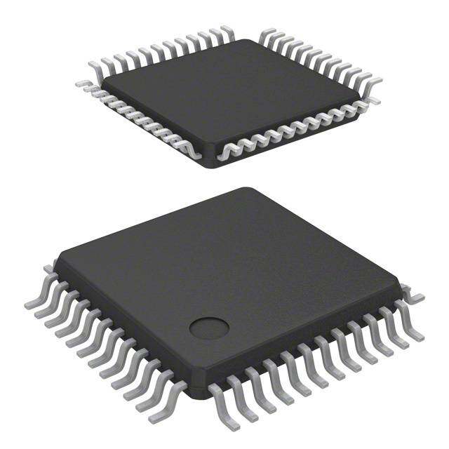
| 描述 | IC CAN CONTROLLER W/SPI 18SOIC网络控制器与处理器 IC W/ SPI Interface |
| 产品分类 | |
| 品牌 | Microchip Technology |
| 产品手册 | |
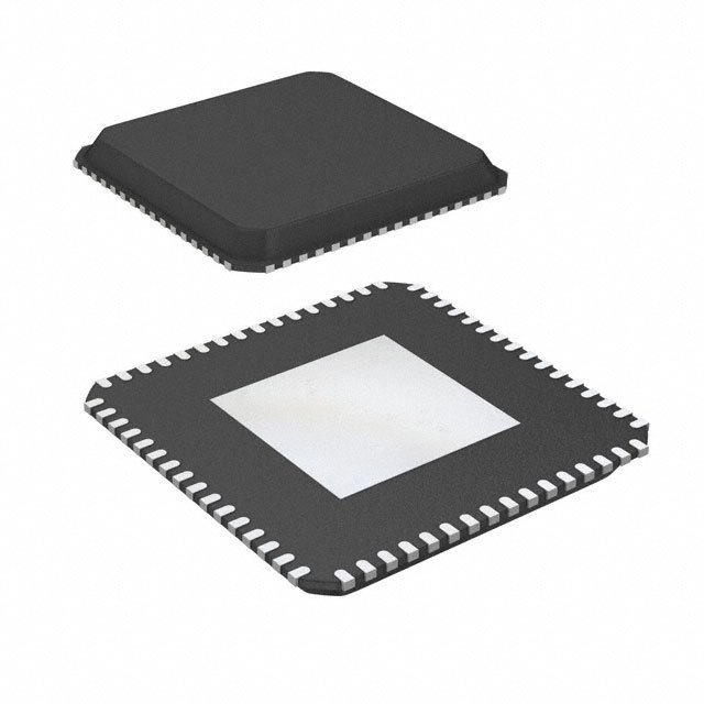
| 产品图片 |
|
| rohs | 符合RoHS无铅 / 符合限制有害物质指令(RoHS)规范要求 |
| 产品系列 | 通信及网络 IC,网络控制器与处理器 IC,Microchip Technology MCP2515-I/SO- |
| 数据手册 | http://www.microchip.com/mymicrochip/filehandler.aspx?ddocname=en011733http://www.microchip.com/mymicrochip/filehandler.aspx?ddocname=en023833http://www.microchip.com/mymicrochip/filehandler.aspx?ddocname=en012300 |
| 产品型号 | MCP2515-I/SO |
| 产品 | Controller Area Network (CAN) |
| 产品培训模块 | http://www.digikey.cn/PTM/IndividualPTM.page?site=cn&lang=zhs&ptm=2429 |
| 产品目录页面 | |
| 产品种类 | Interface |
| 供应商器件封装 | 18-SOIC |
| 其它名称 | MCP2515ISO |
| 功能 | 控制器 |
| 包装 | 管件 |
| 协议 | CAN |
| 商标 | Microchip Technology |
| 安装风格 | SMD/SMT |
| 封装 | Tube |
| 封装/外壳 | 18-SOIC(0.295",7.50mm 宽) |
| 封装/箱体 | SOIC-18 |
| 工作温度 | -40°C ~ 85°C |
| 工作电源电压 | 3.3 V, 5 V |
| 工厂包装数量 | 42 |
| 接口 | SPI |
| 收发器数量 | 1 |
| 数据速率 | 1 Mbps |
| 最大工作温度 | + 85 C |
| 最小工作温度 | - 40 C |
| 标准 | CAN 2.0 |
| 标准包装 | 42 |
| 电压-电源 | 2.7 V ~ 5.5 V |
| 电流-电源 | 10mA |
| 电源电压-最大 | 5.5 V |
| 电源电压-最小 | 2.7 V |
| 电源电流—最大值 | 10 mA |
| 配用 | /product-detail/zh/MCP2515DM-BM/MCP2515DM-BM-ND/1999510/product-detail/zh/MCP2515DM-PTPLS/MCP2515DM-PTPLS-ND/1999509/product-detail/zh/DV251001/DV251001-ND/303506 |


- 商务部:美国ITC正式对集成电路等产品启动337调查
- 曝三星4nm工艺存在良率问题 高通将骁龙8 Gen1或转产台积电
- 太阳诱电将投资9.5亿元在常州建新厂生产MLCC 预计2023年完工
- 英特尔发布欧洲新工厂建设计划 深化IDM 2.0 战略
- 台积电先进制程称霸业界 有大客户加持明年业绩稳了
- 达到5530亿美元!SIA预计今年全球半导体销售额将创下新高
- 英特尔拟将自动驾驶子公司Mobileye上市 估值或超500亿美元
- 三星加码芯片和SET,合并消费电子和移动部门,撤换高东真等 CEO
- 三星电子宣布重大人事变动 还合并消费电子和移动部门
- 海关总署:前11个月进口集成电路产品价值2.52万亿元 增长14.8%


PDF Datasheet 数据手册内容提取
MCP2515 Stand-Alone CAN Controller with SPI Interface Features Description • Implements CAN V2.0B at 1Mb/s: Microchip Technology’s MCP2515 is a stand-alone Controller Area Network (CAN) controller that imple- - 0 to 8-byte length in the data field ments the CAN specification, Version 2.0B. It is capable - Standard and extended data and remote of transmitting and receiving both standard and frames extended data and remote frames. The MCP2515 has • Receive Buffers, Masks and Filters: two acceptance masks and six acceptance filters that - Two receive buffers with prioritized message are used to filter out unwanted messages, thereby storage reducing the host MCU’s overhead. The MCP2515 - Six 29-bit filters interfaces with microcontrollers (MCUs) via an industry standard Serial Peripheral Interface (SPI). - Two 29-bit masks • Data Byte Filtering on the First Two Data Bytes Package Types (applies to standard data frames) 18-Lead PDIP/SOIC • Three Transmit Buffers with Prioritization and Abort Features TXCAN 1 18 V DD • High-Speed SPI Interface (10MHz): RXCAN 2 17 RESET - SPI modes 0,0 and 1,1 CLKOUT/SOF 3 16 CS • One-Shot mode Ensures Message Transmission TX0RTS 4 5 15 SO 1 is Attempted Only One Time TX1RTS 5 25 14 SI P • Clock Out Pin with Programmable Prescaler: TX2RTS 6 C 13 SCK M - Can be used as a clock source for other OSC2 7 12 INT device(s) OSC1 8 11 RX0BF • Start-of-Frame (SOF) Signal is Available for Monitoring the SOF Signal: VSS 9 10 RX1BF - Can be used for time slot-based protocols 20-Lead TSSOP and/or bus diagnostics to detect early bus TXCAN 1 20 VDD degradation RXCAN 2 19 RESET • Interrupt Output Pin with Selectable Enables CLKOUT/SOF 3 18 CS TX0RTS 4 5 17 SO 1 • Buffer Full Output Pins Configurable as: TX1RTS 5 5 16 SI 2 - Interrupt output for each receive buffer NC 6 P 15 NC C - General purpose output TX2RTS 7 M 14 SCK OSC2 8 13 INT • Request-to-Send (RTS) Input Pins Individually OSC1 9 12 RX0BF Configurable as: VSS 10 11 RX1BF - Control pins to request transmission for each 20-Lead QFN* N N T transmit buffer A A E C C D S - General purpose inputs X X D E S R T V R C • Low-Power CMOS Technology: 20 19 18 17 16 - Operates from 2.7V-5.5V CLKOUT 1 15 SO - 5mA active current (typical) TX0RTS 2 14 SI EP - 1µA standby current (typical) (Sleep mode) TX1RTS 3 21 13 NC • Temperature Ranges Supported: NC 4 12 SCK - Industrial (I): -40°C to +85°C TX2RTS 5 11 INT 6 7 8 9 10 - Extended (E): -40°C to +125°C 2 1 D F F C C N B B OS OS G X1 X0 R R * Includes Exposed Thermal Pad (EP); see Table1-1. 2003-2016 Microchip Technology Inc. DS20001801H-page 1
MCP2515 NOTES: DS20001801H-page 2 2003-2016 Microchip Technology Inc.
MCP2515 1.0 DEVICE OVERVIEW 1.2 Control Logic The MCP2515 is a stand-alone CAN controller devel- The control logic block controls the setup and operation oped to simplify applications that require interfacing of the MCP2515 by interfacing to the other blocks in with a CAN bus. A simple block diagram of the order to pass information and control. MCP2515 is shown in Figure1-1. The device consists Interrupt pins are provided to allow greater system of three main blocks: flexibility. There is one multipurpose interrupt pin (as 1. The CAN module, which includes the CAN well as specific interrupt pins) for each of the receive protocol engine, masks, filters, transmit and registers that can be used to indicate a valid message receive buffers. has been received and loaded into one of the receive 2. The control logic and registers that are used to buffers. Use of the specific interrupt pins is optional. configure the device and its operation. The general purpose interrupt pin, as well as status registers (accessed via the SPI interface), can also be 3. The SPI protocol block. used to determine when a valid message has been An example system implementation using the device is received. shown in Figure1-2. Additionally, there are three pins available to initiate 1.1 CAN Module immediate transmission of a message that has been loaded into one of the three transmit registers. Use of The CAN module handles all functions for receiving and these pins is optional, as initiating message transmis- transmitting messages on the CAN bus. Messages are sions can also be accomplished by utilizing control transmitted by first loading the appropriate message buf- registers accessed via the SPI interface. fer and control registers. Transmission is initiated by using control register bits via the SPI interface or by 1.3 SPI Protocol Block using the transmit enable pins. Status and errors can be The MCU interfaces to the device via the SPI interface. checked by reading the appropriate registers. Any Writing to, and reading from, all registers is message detected on the CAN bus is checked for errors accomplished using standard SPI read and write and then matched against the user-defined filters to see commands, in addition to specialized SPI commands. if it should be moved into one of the two receive buffers. FIGURE 1-1: BLOCK DIAGRAM CAN Module RXCAN CS CAN TX and RX Buffers SPI SCK SPI Protocol Interface Engine Masks and Filters Logic SI Bus SO TXCAN Control Logic OSC1 Timing OSC2 Generation INT CLKOUT RX0BF RX1BF TX0RTS Control TX1RTS and Interrupt TX2RTS Registers RESET 2003-2016 Microchip Technology Inc. DS20001801H-page 3
MCP2515 FIGURE 1-2: EXAMPLE SYSTEM IMPLEMENTATION Node Node Node Controller Controller Controller SPI SPI SPI MCP2515 MCP2515 MCP2515 TX RX TX RX TX RX XCVR XCVR XCVR CANH CANL TABLE 1-1: PINOUT DESCRIPTION PDIP/ TSSOP QFN I/O/P Name SOIC Description Alternate Pin Function Pin # Pin # Type Pin # TXCAN 1 1 19 O Transmit output pin to CAN bus — RXCAN 2 2 20 I Receive input pin from CAN bus — CLKOUT 3 3 1 O Clock output pin with programmable Start-of-Frame signal prescaler TX0RTS 4 4 2 I Transmit buffer TXB0 Request-to-Send; General purpose digital input, 100kinternal pull-up to V 100kinternal pull-up to V DD DD TX1RTS 5 5 3 I Transmit buffer TXB1 Request-to-Send; General purpose digital input, 100kinternal pull-up to V 100kinternal pull-up to V DD DD TX2RTS 6 7 5 I Transmit buffer TXB2 Request-to-Send; General purpose digital input, 100kinternal pull-up to V 100kinternal pull-up to V DD DD OSC2 7 8 6 O Oscillator output — OSC1 8 9 7 I Oscillator input External clock input V 9 10 8 P Ground reference for logic and I/O — SS pins RX1BF 10 11 9 O Receive buffer RXB1 interrupt pin or General purpose digital output general purpose digital output RX0BF 11 12 10 O Receive buffer RXB0 interrupt pin or General purpose digital output general purpose digital output INT 12 13 11 O Interrupt output pin — SCK 13 14 12 I Clock input pin for SPI interface — SI 14 16 14 I Data input pin for SPI interface — SO 15 17 15 O Data output pin for SPI interface — CS 16 18 16 I Chip select input pin for SPI interface — RESET 17 19 17 I Active-low device Reset input — V 18 20 18 P Positive supply for logic and I/O pins — DD NC — 6,15 4,13 — No internal connection — Legend: I = Input; O = Output; P = Power DS20001801H-page 4 2003-2016 Microchip Technology Inc.
MCP2515 1.4 Transmit/Receive Buffers/Masks/ Filters The MCP2515 has three transmit and two receive buffers, two acceptance masks (one for each receive buffer) and a total of six acceptance filters. Figure1-3 shows a block diagram of these buffers and their connection to the protocol engine. FIGURE 1-3: CAN BUFFERS AND PROTOCOL ENGINE BLOCK DIAGRAM BUFFERS Acceptance Mask RXM1 Acceptance Filter RXF2 A A Acceptance Mask Acceptance Filter c TXB0 TXB1 TXB2 RXM0 RXF3 c c GE GE GE c Acceptance Filter Acceptance Filter e Q R A Q R A Q R A e RXF0 RXF4 p EFAR S EFAR S EFAR S RTOE S RTOE S RTOE S p t XBLX E XBLX E XBLX E Acceptance Filter Acceptance Filter TAMT M TAMT M TAMT M t RXF1 RXF5 R R M X Identifier Identifier X Message B A B Queue 0 B 1 Control Transmit Byte Sequencer Data Field Data Field PROTOCOL Receive REC Error ENGINE Counter TEC Transmit ErrPas Error BusOff Counter Transmit<7:0> Receive<7:0> Shift<14:0> {Transmit<5:0>, Receive<8:0>} Comparator Protocol Finite SOF State CRC<14:0> Machine Bit Transmit Timing Logic Clock Logic Generator TX RX Configuration Registers 2003-2016 Microchip Technology Inc. DS20001801H-page 5
MCP2515 1.5 CAN Protocol Engine 1.5.3 ERROR MANAGEMENT LOGIC The CAN protocol engine combines several functional The Error Management Logic (EML) is responsible for blocks, shown in Figure1-4 and described below. the Fault confinement of the CAN device. Its two count- ers, the Receive Error Counter (REC) and the Transmit 1.5.1 PROTOCOL FINITE STATE MACHINE Error Counter (TEC), are incremented and decremented by commands from the bit stream processor. Based on The heart of the engine is the Finite State Machine the values of the error counters, the CAN controller is set (FSM). The FSM is a sequencer that controls the into the states: error-active, error-passive or bus-off. sequential data stream between the TX/RX Shift register, the CRC register and the bus line. The FSM 1.5.4 BIT TIMING LOGIC also controls the Error Management Logic (EML) and the parallel data stream between the TX/RX Shift The Bit Timing Logic (BTL) monitors the bus line input registers and the buffers. The FSM ensures that the and handles the bus related bit timing according to the processes of reception, arbitration, transmission and CAN protocol. The BTL synchronizes on a recessive- error signaling are performed according to the CAN to-dominant bus transition at the Start-of-Frame (hard protocol. The automatic retransmission of messages synchronization) and on any further recessive-to- on the bus line is also handled by the FSM. dominant bus line transition if the CAN controller itself does not transmit a dominant bit (resynchronization). 1.5.2 CYCLIC REDUNDANCY CHECK The BTL also provides programmable Time Segments to compensate for the propagation delay time, phase The Cyclic Redundancy Check register generates the shifts and to define the position of the sample point Cyclic Redundancy Check (CRC) code, which is within the bit time. The programming of the BTL transmitted after either the Control Field (for messages depends on the baud rate and external physical delay with 0 data bytes) or the Data Field and is used to times. check the CRC field of incoming messages. FIGURE 1-4: CAN PROTOCOL ENGINE BLOCK DIAGRAM RX Bit Timing Logic Transmit Logic TX SAM REC Sample<2:0> Receive Error Counter TEC StuffReg<5:0> Transmit ErrPas Majority Error Counter Decision BusOff BusMon Comparator CRC<14:0> Protocol SOF FSM Comparator Shift<14:0> (Transmit<5:0>, Receive<7:0>) Receive<7:0> Transmit<7:0> RecData<7:0> TrmData<7:0> Rec/Trm Addr. Interface to Standard Buffer DS20001801H-page 6 2003-2016 Microchip Technology Inc.
MCP2515 2.0 CAN MESSAGE FRAMES a standard CAN frame (11-bit identifier), the standard CAN frame will win arbitration due to the assertion of a The MCP2515 supports standard data frames, extended dominant lDE bit. Also, the SRR bit in an extended data frames and remote frames (standard and CAN frame must be recessive to allow the assertion of extended), as defined in the CAN 2.0B specification. a dominant RTR bit by a node that is sending a standard CAN remote frame. 2.1 Standard Data Frame The SRR and lDE bits are followed by the remaining The CAN standard data frame is shown in Figure2-1. 18 bits of the identifier (Extended lD) and the Remote As with all other frames, the frame begins with a Start- Transmission Request bit. of-Frame (SOF) bit, which is of the dominant state and To enable standard and extended frames to be sent allows hard synchronization of all nodes. across a shared network, the 29-bit extended message The SOF is followed by the arbitration field, consisting identifier is split into 11-bit (Most Significant) and 18-bit of 12 bits: the 11-bit identifier and the Remote (Least Significant) sections. This split ensures that the Transmission Request (RTR) bit. The RTR bit is used lDE bit can remain at the same bit position in both the to distinguish a data frame (RTR bit dominant) from a standard and extended frames. remote frame (RTR bit recessive). Following the arbitration field is the six-bit control field. Following the arbitration field is the control field, The first two bits of this field are reserved and must be consisting of six bits. The first bit of this field is the dominant. The remaining four bits of the control field Identifier Extension (IDE) bit, which must be dominant are the DLC, which specifies the number of data bytes to specify a standard frame. The following bit, Reserved contained in the message. Bit Zero (RB0), is reserved and is defined as a dominant The remaining portion of the frame (data field, CRC bit by the CAN protocol. The remaining four bits of the field, Acknowledge field, End-of-Frame and intermis- control field are the Data Length Code (DLC), which sion) is constructed in the same way as a standard data specifies the number of bytes of data (0-8bytes) frame (see Section2.1 “Standard Data Frame”). contained in the message. After the control field, is the data field, which contains 2.3 Remote Frame any data bytes that are being sent, and is of the length Normally, data transmission is performed on an defined by the DLC (0-8 bytes). autonomous basis by the data source node (e.g., a The Cyclic Redundancy Check (CRC) field follows the sensor sending out a data frame). It is possible, data field and is used to detect transmission errors. The however, for a destination node to request data from the CRC field consists of a 15-bit CRC sequence, followed source. To accomplish this, the destination node sends by the recessive CRC Delimiter bit. a remote frame with an identifier that matches the iden- The final field is the two-bit Acknowledge (ACK) field. tifier of the required data frame. The appropriate data During the ACK Slot bit, the transmitting node sends source node will then send a data frame in response to out a recessive bit. Any node that has received an the remote frame request. error-free frame Acknowledges the correct reception of There are two differences between a remote frame the frame by sending back a dominant bit (regardless (shown in Figure2-3) and a data frame. First, the RTR of whether the node is configured to accept that bit is at the recessive state, and second, there is no specific message or not). The recessive Acknowledge data field. In the event of a data frame and a remote delimiter completes the Acknowledge field and may not frame with the same identifier being transmitted at the be overwritten by a dominant bit. same time, the data frame wins arbitration due to the dominant RTR bit following the identifier. In this way, 2.2 Extended Data Frame the node that transmitted the remote frame receives the desired data immediately. In the extended CAN data frame, shown in Figure2-2, the SOF bit is followed by the arbitration field, which 2.4 Error Frame consists of 32 bits. The first 11 bits are the Most Significant bits (MSb) (Base-lD) of the 29-bit identifier. An error frame is generated by any node that detects a These 11 bits are followed by the Substitute Remote bus error. An error frame, shown in Figure2-4, consists Request (SRR) bit, which is defined to be recessive. of two fields: an error flag field followed by an error The SRR bit is followed by the lDE bit, which is delimiter field. There are two types of error flag fields. recessive to denote an extended CAN frame. The type of error flag field sent depends upon the error It should be noted that if arbitration remains unresolved status of the node that detects and generates the error after transmission of the first 11 bits of the identifier, and flag field. one of the nodes involved in the arbitration is sending 2003-2016 Microchip Technology Inc. DS20001801H-page 7
MCP2515 2.4.1 ACTIVE ERRORS 2.5 Overload Frame If an error-active node detects a bus error, the node An overload frame, shown in Figure2-5, has the same interrupts transmission of the current message by format as an active-error frame. An overload frame, generating an active error flag. The active error flag is however, can only be generated during an interframe composed of six consecutive dominant bits. This bit space. In this way, an overload frame can be sequence actively violates the bit-stuffing rule. All other differentiated from an error frame (an error frame is stations recognize the resulting bit-stuffing error, and in sent during the transmission of a message). The turn, generate error frames themselves, called error overload frame consists of two fields: an overload flag echo flags. followed by an overload delimiter. The overload flag The error flag field, therefore, consists of between six consists of six dominant bits followed by overload flags and twelve consecutive dominant bits (generated by generated by other nodes (and, as for an active error one or more nodes). The error delimiter field (eight flag, giving a maximum of twelve dominant bits). The recessive bits) completes the error frame. Upon overload delimiter consists of eight recessive bits. An completion of the error frame, bus activity returns to overload frame can be generated by a node as a result normal and the interrupted node attempts to resend the of two conditions: aborted message. 1. The node detects a dominant bit during the inter- frame space, an illegal condition. Exception: The Note: Error echo flags typically occur when a dominant bit is detected during the third bit of IFS. localized disturbance causes one or more In this case, the receivers will interpret this as a (but not all) nodes to send an error flag. SOF. The remaining nodes generate error flags 2. Due to internal conditions, the node is not yet in response (echo) to the original error flag. able to begin reception of the next message. A node may generate a maximum of two sequential 2.4.2 PASSIVE ERRORS overload frames to delay the start of the next If an error-passive node detects a bus error, the node message. transmits an error-passive flag followed by the error Note: Case 2 should never occur with the delimiter field. The error-passive flag consists of six MCP2515 due to very short internal consecutive recessive bits. The error frame for an error- delays. passive node consists of 14 recessive bits. From this, it follows that unless the bus error is detected by an error- active node or the transmitting node, the message will 2.6 Interframe Space continue transmission because the error-passive flag The interframe space separates a preceding frame (of does not interfere with the bus. any type) from a subsequent data or remote frame. If the transmitting node generates an error-passive flag, The interframe space is composed of at least three it will cause other nodes to generate error frames due to recessive bits, called the ‘Intermission’. This allows the resulting bit-stuffing violation. After transmission of nodes time for internal processing before the start of an error frame, an error-passive node must wait for six the next message frame. After the intermission, the consecutive recessive bits on the bus before attempting bus line remains in the recessive state (Bus Idle) until to rejoin bus communications. the next transmission starts. The error delimiter consists of eight recessive bits, and allows the bus nodes to restart bus communications cleanly after an error has occurred. DS20001801H-page 8 2003-2016 Microchip Technology Inc.
MCP2515 FIGURE 2-1: STANDARD DATA FRAME 1 S F 1 I 1 1 1 of-me 1 7 d-a 1 EnFr 1 1 1 leD KCA 1 tiB tolS kcA leD CRC 1 d el 6Fi 1C C CR 15CR N) 8 + 4 4 8 = s bit s Frame (number of 8N (0N8)Data Field mit/Receive Buffer Bit-Stuffing a ns Dat 8 Tra n d i e or St 0CLD h 6ontrolField4 3CLD DataLengtCode C 0BR 0 tiB devreseR EDI 0 RTR 0 0DI d s 12Arbitration Fiel 11 3DI Identifier MessageFiltering Stored in Buffer 01 DI emarF-fo-tratS 0 2003-2016 Microchip Technology Inc. DS20001801H-page 9
MCP2515 FIGURE 2-2: EXTENDED DATA FRAME S 1 F 1 I 1 1 1 of-me 1 7 d-a 1 EnFr 1 1 1 leD KCA 1 tiB tolS kcA leD CRC 1 d el 6Fi C 1C 5 R R 1 C C 8 N) s 8 er er of bits = 64 + 8N (0 N 8)Data Field mit/Receive Buff b s m n e (nu 8 n Tra m d i a e Fr or a 0CLD h St Dat 6ControlField 4 3RC10BBTLRRRD 000 stDataiB LengtdeCodevreseR Bit-Stuffing 0DIE er ntifi e d 8 d I 1 e d n e on Field Ext Buffers 32 Arbitrati 71RED0RDDISEII 11 Stored in 3DI 11 Identifier MessageFiltering 01DI emarF-fo-tratS 0 DS20001801H-page 10 2003-2016 Microchip Technology Inc.
MCP2515 FIGURE 2-3: REMOTE FRAME 1 S F 1 I 1 1 1 of-me 1 7 d-a 1 EnFr 1 1 1 leD KCA 1 tiB tolS kcA leD CRC 1 d el 16C Fi 5 RC R 1 C d C el Fi a at D o N 0CLD h 6ontroleld 4 3CLD DataLengtCode CFi 0BR 0 stiB devreseR 1BR 0 RTR 1 0DIE er ntifi e d 8 d I 1 e d en er eld Ext ntifi Fi e 32 Arbitration 71REDRDISEI 11 xtended Id 0DI E h wit 11 3DI Identifier MessageFiltering ote Frame m 01DI Re emarF-fo-tratS 0 2003-2016 Microchip Technology Inc. DS20001801H-page 11
MCP2515 FIGURE 2-4: ACTIVE ERROR FRAME or e c ae pm Frame Soad Fra er-erl IntOv 0 1 1 er 1 8 Error elimit 11 D 1 e 1 m a 1 Fr 0 or 0 Err £ 6 EchoErrorFlag 0 0 0 6 Error Flag 00 0 0 8 orme e a mFr N (0 N 8) Data Field Data FraRemote 8 e m a Fr 8 a at D g pted 0CLD Stuffin Interru 6ontrol eld4 3CLD Data Length Code Bit- C Fi 0BR 0 tiB devreseR EDI 0 RTR 0 0DI d el 3DI 12bitration Fi 11 Identifier Message Filtering Ar 01 DI emarF-fo-tratS 0 DS20001801H-page 12 2003-2016 Microchip Technology Inc.
MCP2515 FIGURE 2-5: OVERLOAD FRAME or e c a p S e e mm aa FrFr nter-Error I 1 1 ame 8 OverloadDelimiter 1111 Fr 1 d 1 a o 0 erl 0 v O d 0 a og 0 6 erlFla 0 v O 0 0 1 1 of-me 1 7 End-tiBFral leteoDDlS CK kRCcCAA 111111 d-of-Frame oror Delimiter orerload Delimiter EnErrOv 4) 4 er of bits = 16 CRC Field 15CRC b m u n e ( m a Fr ote 0CLD m Re 6ntroleld4 3CLD oFi C 0BR 0 EDI 0 RTR 1 0DI d el Fi n 2o 1ati 11 bitr Ar 01 DI emarF-fo-tratS 0 2003-2016 Microchip Technology Inc. DS20001801H-page 13
MCP2515 NOTES: DS20001801H-page 14 2003-2016 Microchip Technology Inc.
MCP2515 3.0 MESSAGE TRANSMISSION 3.3 Initiating Transmission In order to initiate message transmission, the TXREQ 3.1 Transmit Buffers bit (TXBnCTRL<3>) must be set for each buffer to be transmitted. This can be accomplished by: The MCP2515 implements three transmit buffers. Each of these buffers occupies 14 bytes of SRAM and are • Writing to the register via the SPI write command mapped into the device memory map. • Sending the SPI RTS command The first byte, TXBnCTRL, is a control register • Setting the TXnRTS pin low for the particular associated with the message buffer. The information in transmit buffer(s) that are to be transmitted this register determines the conditions under which the If transmission is initiated via the SPI interface, the message will be transmitted and indicates the status of TXREQ bit can be set at the same time as the TXPx the message transmission (see Register3-1). priority bits. Five bytes are used to hold the Standard and Extended When TXREQ is set, the ABTF, MLOA and TXERR bits Identifiers, as well as other message arbitration infor- (TXBnCTRL<5:4>) will be cleared automatically. mation (see Register3-3 through Register3-6). The last eight bytes are for the eight possible data bytes of Note: Setting the TXREQ bit (TXBnCTRL<3>) the message to be transmitted (see Register3-8). does not initiate a message transmission. At a minimum, the TXBnSIDH, TXBnSIDL and TXBnDLC It merely flags a message buffer as being registers must be loaded. If data bytes are present in the ready for transmission. Transmission will message, the TXBnDm registers must also be loaded. start when the device detects that the bus If the message is to use Extended Identifiers, the is available. TXBnEIDm registers must also be loaded and the Once the transmission has completed successfully, the EXIDE (TXBnSIDL<3>) bit set. TXREQ bit will be cleared, the TXnIF bit (CANINTF) will Prior to sending the message, the MCU must initialize be set and an interrupt will be generated if the TXnIE bit the TXnIE bit in the CANINTE register to enable or (CANINTE) is set. disable the generation of an interrupt when the message If the message transmission fails, the TXREQ bit will is sent. remain set. This indicates that the message is still pending for transmission and one of the following Note: The TXREQ bit (TXBnCTRL<3>) must be condition flags will be set: clear (indicating the transmit buffer is not pending transmission) before writing to • If the message started to transmit but the transmit buffer. encountered an error condition, the TXERR (TXBnCTRL<4>) and MERRF bits (CANINTF<7>) 3.2 Transmit Priority will be set, and an interrupt will be generated on the INT pin if the MERRE bit (CANINTE<7>) is set Transmit priority is a prioritization within the MCP2515 • If the message is lost, arbitration at the of the pending transmittable messages. This is MLOA bit (TXBnCTRL<5>) will be set independent from, and not necessarily related to, any prioritization implicit in the message arbitration scheme Note: If One-Shot mode is enabled (OSM bit built into the CAN protocol. (CANCTRL<3>)), the above conditions will still exist. However, the TXREQ bit will be Prior to sending the SOF, the priority of all buffers that cleared and the message will not attempt are queued for transmission is compared. The transmit transmission a second time. buffer with the highest priority will be sent first. For example, if Transmit Buffer 0 has a higher priority setting than Transmit Buffer 1, Transmit Buffer 0 will be 3.4 One-Shot Mode sent first. One-Shot mode ensures that a message will only If two buffers have the same priority setting, the buffer attempt to transmit one time. Normally, if a CAN with the highest buffer number will be sent first. For message loses arbitration, or is destroyed by an error example, if Transmit Buffer 1 has the same priority frame, the message is retransmitted. With One-Shot setting as Transmit Buffer 0, Transmit Buffer 1 will be mode enabled, a message will only attempt to transmit sent first. one time, regardless of arbitration loss or error frame. There are four levels of transmit priority. If the One-Shot mode is required to maintain time slots in TXP<1:0> bits (TXBnCTRL<1:0>) for a particular mes- deterministic systems, such as TTCAN. sage buffer are set to ‘11’, that buffer has the highest possible priority. If the TXP<1:0> bits for a particular message buffer are ‘00’, that buffer has the lowest possible priority. 2003-2016 Microchip Technology Inc. DS20001801H-page 15
MCP2515 3.5 TXnRTS Pins 3.6 Aborting Transmission The TXnRTS pins are input pins that can be configured The MCU can request to abort a message in a specific as: message buffer by clearing the associated TXREQ bit. • Request-to-Send inputs, which provide an In addition, all pending messages can be requested to alternative means of initiating the transmission of be aborted by setting the ABAT bit (CANCTRL<4>). a message from any of the transmit buffers This bit MUST be reset (typically after the TXREQ bits • Standard digital inputs have been verified to be cleared) to continue transmit- ting messages. The ABTF flag (TXBnCTRL<6>) will Configuration and control of these pins is accomplished only be set if the abort was requested via the ABAT bit. using the TXRTSCTRL register (see Register3-2). The Aborting a message by resetting the TXREQ bit does TXRTSCTRL register can only be modified when the NOT cause the ABTF bit to be set. MCP2515 is in Configuration mode (see Section10.0 “Modes of Operation”). If configured to operate as a Note1: Messages that were transmitting when Request-to-Send pin, the pin is mapped into the the abort was requested will continue to respective TXREQ bit (TXBnCTRL<3>) for the transmit transmit. If the message does not suc- buffer. The TXREQ bit is latched by the falling edge of cessfully complete transmission (i.e., lost the TXnRTS pin. The TXnRTS pins are designed to arbitration or was interrupted by an error allow them to be tied directly to the RXnBF pins to frame), it will then be aborted. automatically initiate a message transmission when the RXnBF pin goes low. 2: When One-Shot mode is enabled, if the message is interrupted due to an error The TXnRTS pins have internal pull-up resistors of frame or loss of arbitration, the ABTF bit 100k (nominal). will set. DS20001801H-page 16 2003-2016 Microchip Technology Inc.
MCP2515 FIGURE 3-1: TRANSMIT MESSAGE FLOWCHART Start The message transmission sequence begins when the device determines that the TXREQ bit (TXBnCTRL<3>) for any of the transmit registers has been set. No Are any TXREQ (TXBnCTRL<3>) bits = 1? Yes Clearing the TXREQ bit while it is set, Clear: or setting the ABAT bit (CANCTRL<4>) ABTF (TXBnCTRL<6>) before the message has started MLOA (TXBnCTRL<5>) transmission, will abort the message. TXERR (TXBnCTRL<4>) Is Is CAN bus available No TXREQ = 0 No to start transmission? or ABAT = 1? Yes Yes Examine TXP<1:0> (TXBnCTRL<1:0>) to Determine Highest Priority Message Transmit Message Message Was No Message error Error Message Transmitted or Successfully? lost arbitration ? Set TXERR (TXBnCTRL<4>) Yes Lost Arbitration Clear TXREQ bit Yes MERRE (CANINTE)? Yes Set GInetenrerruaptet TXnIE (CANINTE) = 1? MLOA (TXBnCTRL<5>) No Generate Interrupt No Set Set TXnIF (CANTINF) MERRF (CANTINF) The TXnIE bit determines if an interrupt should be generated when a message is successfully transmitted. GOTO START 2003-2016 Microchip Technology Inc. DS20001801H-page 17
MCP2515 REGISTER 3-1: TXBnCTRL: TRANSMIT BUFFER n CONTROL REGISTER (ADDRESS: 30h, 40h, 50h) U-0 R-0 R-0 R-0 R/W-0 U-0 R/W-0 R/W-0 — ABTF MLOA TXERR TXREQ — TXP1 TXP0 bit 7 bit 0 Legend: R = Readable bit W = Writable bit U = Unimplemented bit, read as ‘0’ -n = Value at POR ‘1’ = Bit is set ‘0’ = Bit is cleared x = Bit is unknown bit 7 Unimplemented: Read as ‘0’ bit 6 ABTF: Message Aborted Flag bit 1 = Message was aborted 0 = Message completed transmission successfully bit 5 MLOA: Message Lost Arbitration bit 1 = Message lost arbitration while being sent 0 = Message did not lose arbitration while being sent bit 4 TXERR: Transmission Error Detected bit 1 = A bus error occurred while the message was being transmitted 0 = No bus error occurred while the message was being transmitted bit 3 TXREQ: Message Transmit Request bit 1 = Buffer is currently pending transmission (MCU sets this bit to request message be transmitted – bit is automatically cleared when the message is sent) 0 = Buffer is not currently pending transmission (MCU can clear this bit to request a message abort) bit 2 Unimplemented: Read as ‘0’ bit 1-0 TXP<1:0>: Transmit Buffer Priority bits 11 = Highest message priority 10 = High intermediate message priority 01 = Low intermediate message priority 00 = Lowest message priority DS20001801H-page 18 2003-2016 Microchip Technology Inc.
MCP2515 REGISTER 3-2: TXRTSCTRL: TXnRTS PIN CONTROL AND STATUS REGISTER (ADDRESS: 0Dh) U-0 U-0 R-x R-x R-x R/W-0 R/W-0 R/W-0 — — B2RTS B1RTS B0RTS B2RTSM B1RTSM B0RTSM bit 7 bit 0 Legend: R = Readable bit W = Writable bit U = Unimplemented bit, read as ‘0’ -n = Value at POR ‘1’ = Bit is set ‘0’ = Bit is cleared x = Bit is unknown bit 7-6 Unimplemented: Read as ‘0’ bit 5 B2RTS: TX2RTS Pin State bit - Reads state of TX2RTS pin when in Digital Input mode - Reads as ‘0’ when pin is in Request-to-Send mode bit 4 B1RTS: TX1RTS Pin State bit - Reads state of TX1RTS pin when in Digital Input mode - Reads as ‘0’ when pin is in Request-to-Send mode bit 3 B0RTS: TX0RTS Pin State bit - Reads state of TX0RTS pin when in Digital Input mode - Reads as ‘0’ when pin is in Request-to-Send mode bit 2 B2RTSM: TX2RTS Pin mode bit 1 = Pin is used to request message transmission of TXB2 buffer (on falling edge) 0 = Digital input bit 1 B1RTSM: TX1RTS Pin mode bit 1 = Pin is used to request message transmission of TXB1 buffer (on falling edge) 0 = Digital input bit 0 B0RTSM: TX0RTS Pin mode bit 1 = Pin is used to request message transmission of TXB0 buffer (on falling edge) 0 = Digital input 2003-2016 Microchip Technology Inc. DS20001801H-page 19
MCP2515 REGISTER 3-3: TXBnSIDH: TRANSMIT BUFFER n STANDARD IDENTIFIER REGISTER HIGH (ADDRESS: 31h, 41h, 51h) R/W-x R/W-x R/W-x R/W-x R/W-x R/W-x R/W-x R/W-x SID10 SID9 SID8 SID7 SID6 SID5 SID4 SID3 bit 7 bit 0 Legend: R = Readable bit W = Writable bit U = Unimplemented bit, read as ‘0’ -n = Value at POR ‘1’ = Bit is set ‘0’ = Bit is cleared x = Bit is unknown bit 7-0 SID<10:3>: Standard Identifier bits REGISTER 3-4: TXBnSIDL: TRANSMIT BUFFER n STANDARD IDENTIFIER REGISTER LOW (ADDRESS: 32h, 42h, 52h) R/W-x R/W-x R/W-x U-0 R/W-x U-0 R/W-x R/W-x SID2 SID1 SID0 — EXIDE — EID17 EID16 bit 7 bit 0 Legend: R = Readable bit W = Writable bit U = Unimplemented bit, read as ‘0’ -n = Value at POR ‘1’ = Bit is set ‘0’ = Bit is cleared x = Bit is unknown bit 7-5 SID<2:0>: Standard Identifier bits bit 4 Unimplemented: Read as ‘0’ bit 3 EXIDE: Extended Identifier Enable bit 1 = Message will transmit Extended Identifier 0 = Message will transmit Standard Identifier bit 2 Unimplemented: Read as ‘0’ bit 1-0 EID<17:16>: Extended Identifier bits DS20001801H-page 20 2003-2016 Microchip Technology Inc.
MCP2515 REGISTER 3-5: TXBnEID8: TRANSMIT BUFFER n EXTENDED IDENTIFIER 8 REGISTER HIGH (ADDRESS: 33h, 43h, 53h) R/W-x R/W-x R/W-x R/W-x R/W-x R/W-x R/W-x R/W-x EID15 EID14 EID13 EID12 EID11 EID10 EID9 EID8 bit 7 bit 0 Legend: R = Readable bit W = Writable bit U = Unimplemented bit, read as ‘0’ -n = Value at POR ‘1’ = Bit is set ‘0’ = Bit is cleared x = Bit is unknown bit 7-0 EID<15:8>: Extended Identifier bits REGISTER 3-6: TXBnEID0: TRANSMIT BUFFER n EXTENDED IDENTIFIER 0 REGISTER LOW (ADDRESS: 34h, 44h, 54h) R/W-x R/W-x R/W-x R/W-x R/W-x R/W-x R/W-x R/W-x EID7 EID6 EID5 EID4 EID3 EID2 EID1 EID0 bit 7 bit 0 Legend: R = Readable bit W = Writable bit U = Unimplemented bit, read as ‘0’ -n = Value at POR ‘1’ = Bit is set ‘0’ = Bit is cleared x = Bit is unknown bit 7-0 EID<7:0>: Extended Identifier bits 2003-2016 Microchip Technology Inc. DS20001801H-page 21
MCP2515 REGISTER 3-7: TXBnDLC: TRANSMIT BUFFER n DATA LENGTH CODE REGISTER (ADDRESS: 35h, 45h, 55h) U-0 R/W-x U-0 U-0 R/W-x R/W-x R/W-x R/W-x — RTR — — DLC3(1) DLC2(1) DLC1(1) DLC0(1) bit 7 bit 0 Legend: R = Readable bit W = Writable bit U = Unimplemented bit, read as ‘0’ -n = Value at POR ‘1’ = Bit is set ‘0’ = Bit is cleared x = Bit is unknown bit 7 Unimplemented: Read as ‘0’ bit 6 RTR: Remote Transmission Request bit 1 = Transmitted message will be a remote transmit request 0 = Transmitted message will be a data frame bit 5-4 Unimplemented: Reads as ‘0’ bit 3-0 DLC<3:0>: Data Length Code bits(1) Sets the number of data bytes to be transmitted (0 to 8 bytes). Note 1: It is possible to set the DLC<3:0> bits to a value greater than eight; however, only eight bytes are transmitted. REGISTER 3-8: TXBnDm: TRANSMIT BUFFER n DATA BYTE m REGISTER (ADDRESS: 36h-3Dh, 46h-4Dh, 56h-5Dh) R/W-x R/W-x R/W-x R/W-x R/W-x R/W-x R/W-x R/W-x TXBnDm7 TXBnDm6 TXBnDm5 TXBnDm4 TXBnDm3 TXBnDm2 TXBnDm1 TXBnDm0 bit 7 bit 0 Legend: R = Readable bit W = Writable bit U = Unimplemented bit, read as ‘0’ -n = Value at POR ‘1’ = Bit is set ‘0’ = Bit is cleared x = Bit is unknown bit 7-0 TXBnDm<7:0>: Transmit Buffer n Data Field Byte m bits DS20001801H-page 22 2003-2016 Microchip Technology Inc.
MCP2515 4.0 MESSAGE RECEPTION 4.2 Receive Priority RXB0, the higher priority buffer, has one mask and two 4.1 Receive Message Buffering message acceptance filters associated with it. The received message is applied to the mask and filters for The MCP2515 includes two full receive buffers with RXB0 first. multiple acceptance filters for each. There is also a separate Message Assembly Buffer (MAB) that acts as RXB1 is the lower priority buffer, with one mask and a third receive buffer (see Figure4-2). four acceptance filters associated with it. In addition to the message being applied to the RXB0 4.1.1 MESSAGE ASSEMBLY BUFFER mask and filters first, the lower number of acceptance Of the three receive buffers, the MAB is always filters makes the match on RXB0 more restrictive and committed to receiving the next message from the bus. implies a higher priority for that buffer. The MAB assembles all messages received. These When a message is received, the RXBnCTRL<3:0> messages will be transferred to the RXBn buffers (see register bits will indicate the acceptance filter number Register4-4 to Register4-9) only if the acceptance that enabled reception and whether the received filter criteria is met. message is a Remote Transfer Request. 4.1.2 RXB0 AND RXB1 4.2.1 ROLLOVER The remaining two receive buffers, called RXB0 and Additionally, the RXB0CTRL register can be configured RXB1, can receive a complete message from the such that, if RXB0 contains a valid message and protocol engine via the MAB. The MCU can access one another valid message is received, an overflow error buffer, while the other buffer is available for message will not occur and the new message will be moved into reception, or for holding a previously received RXB1, regardless of the acceptance criteria of RXB1. message. 4.2.2 RXM BITS Note: The entire content of the MAB is moved into the receive buffer once a message is The RXM<1:0> bits (RXBnCTRL<6:5>) set special accepted. This means, that regardless of Receive modes. Normally, these bits are cleared to ‘00’ the type of identifier (Standard or to enable reception of all valid messages as deter- Extended) and the number of data bytes mined by the appropriate acceptance filters. In this received, the entire receive buffer is case, the determination of whether or not to receive overwritten with the MAB contents. standard or extended messages is determined by the Therefore, the contents of all registers in EXIDE bit (RFXnSIDL<3>) in the Filter n Standard the buffer must be assumed to have been Identifier Low register. modified when any message is received. If the RXM<1:0> bits are set to ‘11’, the buffer will receive all messages, regardless of the values of the 4.1.3 RECEIVE FLAGS/INTERRUPTS acceptance filters. Also, if a message has an error before the EOF, that portion of the message assembled When a message is moved into either of the receive in the MAB, before the error frame, will be loaded into buffers, the appropriate RXnIF bit (CANINTF) is set. the buffer. This mode has some value in debugging a This bit must be cleared by the MCU in order to allow a CAN system and would not be used in an actual new message to be received into the buffer. This bit system environment. provides a positive lockout to ensure that the MCU has finished with the message before the MCP2515 Setting the RXM<1:0> bits to ‘01’ or ‘10’ is not attempts to load a new message into the receive buffer. recommended. If the RXnIE bit (CANINTE) is set, an interrupt will be generated on the INT pin to indicate that a valid message has been received. In addition, the associ- ated RXnBF pin will drive low if configured as a receive buffer full pin. See Section4.4 “RX0BF and RX1BF Pins” for details. 2003-2016 Microchip Technology Inc. DS20001801H-page 23
MCP2515 4.3 Start-of-Frame Signal 4.4.1 DISABLED If enabled, the Start-of-Frame signal is generated on The RXnBF pins can be disabled to the high-impedance the SOF pin at the beginning of each CAN message state by clearing the BnBFE bits (BFPCTRL<3:2>). detected on the RXCAN pin. 4.4.2 CONFIGURED AS BUFFER FULL The RXCAN pin monitors an Idle bus for a recessive- to-dominant edge. If the dominant condition remains The RXnBF pins can be configured to act as either buf- until the sample point, the MCP2515 interprets this as fer full interrupt pins or as standard digital outputs. a SOF and a SOF pulse is generated. If the dominant Configuration and status of these pins are available via condition does not remain until the sample point, the the BFPCTRL register (Register4-3). When set to MCP2515 interprets this as a glitch on the bus and no operate in Interrupt mode, by setting the BnBFE and SOF signal is generated. Figure4-1 illustrates SOF BnBFM bits (BFPCTRL<3:0>), these pins are active- signaling and glitch filtering. low and are mapped to the RXnIF bit (CANINTF) for each receive buffer. When this bit goes high for one of As with One-Shot mode, one use for SOF signaling is the receive buffers (indicating that a valid message has for TTCAN-type systems. In addition, by monitoring been loaded into the buffer), the corresponding RXnBF both the RXCAN pin and the SOF pin, an MCU can pin will go low. When the RXnIF bit is cleared by the detect early physical bus problems by detecting small MCU, the corresponding interrupt pin will go to the logic glitches before they affect the CAN communications. high state until the next message is loaded into the receive buffer. 4.4 RX0BF and RX1BF Pins In addition to the INT pin, which provides an interrupt signal to the MCU for many different conditions, the Receive Buffer Full pins (RX0BF and RX1BF) can be used to indicate that a valid message has been loaded into RXB0 or RXB1, respectively. The pins have three different configurations (Table4-1): 1. Disabled 2. Buffer Full Interrupt 3. Digital Output FIGURE 4-1: START-OF-FRAME SIGNALING Normal SOF Signaling START-OF-FRAME BIT ID Bit Sample Point RXCAN SOF Glitch Filtering EXPECTED START-OF-FRAME BIT Expected Sample Bus Idle Point RXCAN SOF DS20001801H-page 24 2003-2016 Microchip Technology Inc.
MCP2515 4.4.3 CONFIGURED AS DIGITAL OUTPUT TABLE 4-1: CONFIGURING RXnBF PINS When used as digital outputs, the BnBFM bits BnBFE BnBFM BnBFS Pin Status (BFPCTRL<1:0>) must be cleared and the BnBFE bits 0 X X Disabled, high-impedance (BFPCTRL<3:2>) must be set for the associated buffer. In this mode, the state of the pin is controlled by the 1 1 X Receive buffer interrupt BnBFS bits (BFPCTRL<5:4>). Writing a ‘1’ to a BnBFS 1 0 0 Digital output = 0 bit will cause a high level to be driven on the associated 1 0 1 Digital output = 1 buffer full pin, while a ‘0’ will cause the pin to drive low. When using the pins in this mode, the state of the pin should be modified only by using the SPI BIT MODIFY command to prevent glitches from occurring on either of the buffer full pins. FIGURE 4-2: RECEIVE BUFFER BLOCK DIAGRAM Note: Messages received in the MAB are initially applied to the mask and filters of RXB0. In addition, only one filter match occurs (e.g., Acceptance Mask if the message matches both RXF0 and RXM1 RXF2, the match will be for RXF0 and the message will be moved into RXB0). Acceptance Filter RXF2 Acceptance Mask Acceptance Filter RXM0 RXF3 A c Acceptance Filter Acceptance Filter c RXF0 RXF4 e A p c t c Acceptance Filter Acceptance Filter e RXF1 RXF5 p t R R Identifier M Identifier X X A B B B 0 1 Data Field Data Field 2003-2016 Microchip Technology Inc. DS20001801H-page 25
MCP2515 FIGURE 4-3: RECEIVE FLOWCHART Start Detect No Start of Message? Yes Begin Loading Message into Message Assembly Buffer (MAB) Generate No Valid Error Message Frame Received? Yes Yes Meets No Meets Yes a Filter Criteria a Filter Criteria for RXB0? for RXB1? No Go to Start Determines if the Receive register is empty and able to accept a new message. Determines if RXB0 can roll over into RXB1 if it is full. Is No Is Yes RX0IF (CANINTF) BUKT (RXB0CTRL<2>) = 0? = 1? Yes No Move Message into RXB0 Generate Overflow Error: Generate Overflow Error: No RX1IF (CAIsNINTF<3>) Set RX0OVR (EFLG<6>) Set RX1OVR (EFLG<7>) = 0? Set RX0IF (CANINTF<0>) = 1 Yes Move Message into RXB1 Is No Set FILHIT0 (RXB0CTRL<0>) ERRIE (CANINTE<5>) According to Which Filter Criteria = 1? Set RX1IF (CANINTF<3>) = 1 Yes Set FILHIT<2:0> (RXB1CTRL<2:0>) Generate Go to Start According to which Filter Criteria Interrupt on INT was Met RX0IE (CANINTE<0>) Yes Generate Yes RX1IE (CANINTE<1>) Interrupt on INT = 1? = 1? No RXB0 Set CANSTAT<3:0> according RXB1 No to which receive buffer the message was loaded into Are Are B0BFM (BFPanCdTRL<0>) = 1 Yes Set RXBF0 Set RXBF1 Yes B1BFM (BFPanCdTRL<1>) = 1 B0BFE (BFPCTRL<2>) = 1? Pin = 0 Pin = 0 B1BFE (BF1CTRL<3>) = 1? No No DS20001801H-page 26 2003-2016 Microchip Technology Inc.
MCP2515 REGISTER 4-1: RXB0CTRL: RECEIVE BUFFER 0 CONTROL REGISTER (ADDRESS: 60h) U-0 R/W-0 R/W-0 U-0 R-0 R/W-0 R-0 R-0 — RXM1 RXM0 — RXRTR BUKT BUKT1 FILHIT0(1) bit 7 bit 0 Legend: R = Readable bit W = Writable bit U = Unimplemented bit, read as ‘0’ -n = Value at POR ‘1’ = Bit is set ‘0’ = Bit is cleared x = Bit is unknown bit 7 Unimplemented: Read as ‘0’ bit 6-5 RXM<1:0>: Receive Buffer Operating mode bits 11 = Turns mask/filters off; receives any message 10 = Reserved 01 = Reserved 00 = Receives all valid messages using either Standard or Extended Identifiers that meet filter criteria; Extended ID Filter registers, RXFnEID8:RXFnEID0, are applied to the first two bytes of data in the messages with standard IDs bit 4 Unimplemented: Read as ‘0’ bit 3 RXRTR: Received Remote Transfer Request bit 1 = Remote Transfer Request received 0 = No Remote Transfer Request received bit 2 BUKT: Rollover Enable bit 1 = RXB0 message will roll over and be written to RXB1 if RXB0 is full 0 = Rollover is disabled bit 1 BUKT1: Read-Only Copy of BUKT bit (used internally by the MCP2515) bit 0 FILHIT0: Filter Hit bit (indicates which acceptance filter enabled reception of message)(1) 1 = Acceptance Filter 1 (RXF1) 0 = Acceptance Filter 0 (RXF0) Note 1: If a rollover from RXB0 to RXB1 occurs, the FILHIT0 bit will reflect the filter that accepted the message that rolled over. 2003-2016 Microchip Technology Inc. DS20001801H-page 27
MCP2515 REGISTER 4-2: RXB1CTRL: RECEIVE BUFFER 1 CONTROL REGISTER (ADDRESS: 70h) U-0 R/W-0 R/W-0 U-0 R-0 R-0 R-0 R-0 — RXM1 RXM0 — RXRTR FILHIT2 FILHIT1 FILHIT0 bit 7 bit 0 Legend: R = Readable bit W = Writable bit U = Unimplemented bit, read as ‘0’ -n = Value at POR ‘1’ = Bit is set ‘0’ = Bit is cleared x = Bit is unknown bit 7 Unimplemented: Read as ‘0’ bit 6-5 RXM<1:0>: Receive Buffer Operating mode bits 11 = Turns mask/filters off; receives any message 10 = Reserved 01 = Reserved 00 = Receives all valid messages using either Standard or Extended Identifiers that meet filter criteria bit 4 Unimplemented: Read as ‘0’ bit 3 RXRTR: Received Remote Transfer Request bit 1 = Remote Transfer Request received 0 = No Remote Transfer Request received bit 2-0 FILHIT<2:0>: Filter Hit bits (indicates which acceptance filter enabled reception of message) 101 = Acceptance Filter 5 (RXF5) 100 = Acceptance Filter 4 (RXF4) 011 = Acceptance Filter 3 (RXF3) 010 = Acceptance Filter 2 (RXF2) 001 = Acceptance Filter 1 (RXF1) (only if the BUKT bit is set in RXB0CTRL) 000 = Acceptance Filter 0 (RXF0) (only if the BUKT bit is set in RXB0CTRL) DS20001801H-page 28 2003-2016 Microchip Technology Inc.
MCP2515 REGISTER 4-3: BFPCTRL: RXnBF PIN CONTROL AND STATUS REGISTER (ADDRESS: 0Ch) U-0 U-0 R/W-0 R/W-0 R/W-0 R/W-0 R/W-0 R/W-0 — — B1BFS B0BFS B1BFE B0BFE B1BFM B0BFM bit 7 bit 0 Legend: R = Readable bit W = Writable bit U = Unimplemented bit, read as ‘0’ -n = Value at POR ‘1’ = Bit is set ‘0’ = Bit is cleared x = Bit is unknown bit 7-6 Unimplemented: Read as ‘0’ bit 5 B1BFS: RX1BF Pin State bit (Digital Output mode only) - Reads as ‘0’ when RX1BF is configured as an interrupt pin bit 4 B0BFS: RX0BF Pin State bit (Digital Output mode only) - Reads as ‘0’ when RX0BF is configured as an interrupt pin bit 3 B1BFE: RX1BF Pin Function Enable bit 1 = Pin function is enabled, operation mode is determined by the B1BFM bit 0 = Pin function is disabled, pin goes to a high-impedance state bit 2 B0BFE: RX0BF Pin Function Enable bit 1 = Pin function is enabled, operation mode is determined by the B0BFM bit 0 = Pin function is disabled, pin goes to a high-impedance state bit 1 B1BFM: RX1BF Pin Operation mode bit 1 = Pin is used as an interrupt when a valid message is loaded into RXB1 0 = Digital Output mode bit 0 B0BFM: RX0BF Pin Operation mode bit 1 = Pin is used as an interrupt when a valid message is loaded into RXB0 0 = Digital Output mode 2003-2016 Microchip Technology Inc. DS20001801H-page 29
MCP2515 REGISTER 4-4: RXBnSIDH: RECEIVE BUFFER n STANDARD IDENTIFIER REGISTER HIGH (ADDRESS: 61h, 71h) R-x R-x R-x R-x R-x R-x R-x R-x SID10 SID9 SID8 SID7 SID6 SID5 SID4 SID3 bit 7 bit 0 Legend: R = Readable bit W = Writable bit U = Unimplemented bit, read as ‘0’ -n = Value at POR ‘1’ = Bit is set ‘0’ = Bit is cleared x = Bit is unknown bit 7-0 SID<10:3>: Standard Identifier bits These bits contain the eight Most Significant bits of the Standard Identifier for the received message. REGISTER 4-5: RXBnSIDL: RECEIVE BUFFER n STANDARD IDENTIFIER REGISTER LOW (ADDRESS: 62h, 72h) R-x R-x R-x R-x R-x U-0 R-x R-x SID2 SID1 SID0 SRR IDE — EID17 EID16 bit 7 bit 0 Legend: R = Readable bit W = Writable bit U = Unimplemented bit, read as ‘0’ -n = Value at POR ‘1’ = Bit is set ‘0’ = Bit is cleared x = Bit is unknown bit 7-5 SID<2:0>: Standard Identifier bits These bits contain the three Least Significant bits of the Standard Identifier for the received message. bit 4 SRR: Standard Frame Remote Transmit Request bit (valid only if IDE bit = 0) 1 = Standard frame Remote Transmit Request received 0 = Standard data frame received bit 3 IDE: Extended Identifier Flag bit This bit indicates whether the received message was a standard or an extended frame. 1 = Received message was an extended frame 0 = Received message was a standard frame bit 2 Unimplemented: Read as ‘0’ bit 1-0 EID<17:16>: Extended Identifier bits These bits contain the two Most Significant bits of the Extended Identifier for the received message. DS20001801H-page 30 2003-2016 Microchip Technology Inc.
MCP2515 REGISTER 4-6: RXBnEID8: RECEIVE BUFFER n EXTENDED IDENTIFIER REGISTER HIGH (ADDRESS: 63h, 73h) R-x R-x R-x R-x R-x R-x R-x R-x EID15 EID14 EID13 EID12 EID11 EID10 EID9 EID8 bit 7 bit 0 Legend: R = Readable bit W = Writable bit U = Unimplemented bit, read as ‘0’ -n = Value at POR ‘1’ = Bit is set ‘0’ = Bit is cleared x = Bit is unknown bit 7-0 EID<15:8>: Extended Identifier bits These bits hold bits 15 through 8 of the Extended Identifier for the received message REGISTER 4-7: RXBnEID0: RECEIVE BUFFER n EXTENDED IDENTIFIER REGISTER LOW (ADDRESS: 64h, 74h) R-x R-x R-x R-x R-x R-x R-x R-x EID7 EID6 EID5 EID4 EID3 EID2 EID1 EID0 bit 7 bit 0 Legend: R = Readable bit W = Writable bit U = Unimplemented bit, read as ‘0’ -n = Value at POR ‘1’ = Bit is set ‘0’ = Bit is cleared x = Bit is unknown bit 7-0 EID<7:0>: Extended Identifier bits These bits hold the Least Significant eight bits of the Extended Identifier for the received message. 2003-2016 Microchip Technology Inc. DS20001801H-page 31
MCP2515 REGISTER 4-8: RXBnDLC: RECEIVE BUFFER n DATA LENGTH CODE REGISTER (ADDRESS: 65h, 75h) U-0 R-x R-x R-x R-x R-x R-x R-x — RTR RB1 RB0 DLC3 DLC2 DLC1 DLC0 bit 7 bit 0 Legend: R = Readable bit W = Writable bit U = Unimplemented bit, read as ‘0’ -n = Value at POR ‘1’ = Bit is set ‘0’ = Bit is cleared x = Bit is unknown bit 7 Unimplemented: Read as ‘0’ bit 6 RTR: Extended Frame Remote Transmission Request bit (valid only when IDE (RXBnSIDL<3>) = 1) 1 = Extended frame Remote Transmit Request received 0 = Extended data frame received bit 5 RB1: Reserved Bit 1 bit 4 RB0: Reserved Bit 0 bit 3-0 DLC<3:0>: Data Length Code bits Indicates the number of data bytes that were received. REGISTER 4-9: RXBnDm: RECEIVE BUFFER n DATA BYTE m REGISTER (ADDRESS: 66h-6Dh, 76h-7Dh) R-x R-x R-x R-x R-x R-x R-x R-x RBnD7 RBnD6 RBnD5 RBnD4 RBnD3 RBnD2 RBnD1 RBnD0 bit 7 bit 0 Legend: R = Readable bit W = Writable bit U = Unimplemented bit, read as ‘0’ -n = Value at POR ‘1’ = Bit is set ‘0’ = Bit is cleared x = Bit is unknown bit 7-0 RBnD<7:0>: Receive Buffer n Data Field Bytes m bits Eight bytes containing the data bytes for the received message. DS20001801H-page 32 2003-2016 Microchip Technology Inc.
MCP2515 4.5 Message Acceptance Filters and identifier is compared to the masks and filters to deter- Masks mine if the message should be loaded into a receive buffer. The mask essentially determines which bits to The message acceptance filters and masks are used to apply the acceptance filters to. If any mask bit is set to determine if a message in the Message Assembly Buffer a zero, that bit will automatically be accepted, should be loaded into either of the receive buffers (see regardless of the filter bit. Figure4-5). Once a valid message has been received into the MAB, the identifier fields of the message are com- TABLE 4-2: FILTER/MASK TRUTH TABLE pared to the filter values. If there is a match, that message Message will be loaded into the appropriate receive buffer. Accept or Mask Bit n Filter Bit n Identifier Reject Bit n 4.5.1 DATA BYTE FILTERING Bit When receiving standard data frames (11-bit identifier), 0 x x Accept the MCP2515 automatically applies 16 bits of masks 1 0 0 Accept and filters, normally associated with Extended 1 0 1 Reject Identifiers, to the first 16 bits of the data field (Data 1 1 0 Reject Bytes 0 and 1). Figure4-4 illustrates how masks and filters apply to extended and standard data frames. 1 1 1 Accept Data byte filtering reduces the load on the MCU when Note: x = don’t care implementing Higher Layer Protocols (HLPs) that filter As shown in the Receive Buffer Block Diagram on the first data byte (e.g., DeviceNet™). (Figure4-2), acceptance filters, RXF0 and RXF1 (and filter mask, RXM0), are associated with RXB0. The 4.5.2 FILTER MATCHING filters, RXF2, RXF3, RXF4, RXF5 and mask RXM1, are The filter masks (see Register4-14 through associated with RXB1. Register4-17) are used to determine which bits in the identifier are examined with the filters. A truth table is shown in Table4-2 that indicates how each bit in the FIGURE 4-4: MASKS AND FILTERS APPLY TO CAN FRAMES Extended Frame ID10 ID0 EID17 EID0 Masks and Filters Apply to the Entire 29-Bit ID Field Standard Data Frame ID10 ID0 * Data Byte 0 Data Byte 1 11-Bit ID Standard Frame 16-Bit Data Filtering* *The two MSbs’ (EID17 and EID16) mask and filter bits are not used. 2003-2016 Microchip Technology Inc. DS20001801H-page 33
MCP2515 4.5.3 FILHIT BITS If the BUKT bit is clear, there are six codes corresponding to the six filters. If the BUKT bit is set, Filter matches on received messages can be determined there are six codes corresponding to the six filters, plus by the FILHIT bits in the associated RXBnCTRL register; two additional codes corresponding to the RXF0 and FILHIT0 (RXB0CTRL<0>) for Buffer 0 and FILHIT<2:0> RXF1 filters that roll over into RXB1. (RXB1CTRL<2:0>) for Buffer 1. The three FILHITn bits for Receive Buffer 1 (RXB1) are 4.5.4 MULTIPLE FILTER MATCHES coded as follows: If more than one acceptance filter matches, the • 101 = Acceptance Filter 5 (RXF5) FILHITn bits will encode the binary value of the lowest • 100 = Acceptance Filter 4 (RXF4) numbered filter that matched. For example, if filters, RXF2 and RXF4, match, the FILHITn bits will be loaded • 011 = Acceptance Filter 3 (RXF3) with the value for RXF2. This essentially prioritizes the • 010 = Acceptance Filter 2 (RXF2) acceptance filters with a lower numbered filter having • 001 = Acceptance Filter 1 (RXF1) higher priority. Messages are compared to filters in • 000 = Acceptance Filter 0 (RXF0) ascending order of filter number. This also ensures that the message will only be received into one buffer. This Note: ‘000’ and ‘001’ can only occur if the BUKT implies that RXB0 has a higher priority than RXB1. bit in RXB0CTRL is set, allowing RXB0 messages to roll over into RXB1. 4.5.5 CONFIGURING THE MASKS AND RXB0CTRL contains two copies of the BUKT bit and a FILTERS copy of the FILHIT0 bit. The Mask and Filter registers can only be modified The coding of the BUKT bit enables these three bits to be when the MCP2515 is in Configuration mode (see used similarly to the FILHIT<2:0> (RXB1CTRL<2:0>) bits Section10.0 “Modes of Operation”). and to distinguish a hit on filters, RXF0 and RXF1, in either RXB0 or after a rollover into RXB1. Note: The Mask and Filter registers read all ‘0’s when in any mode except Configuration • 111 = Acceptance Filter 1 (RXB1) mode. • 110 = Acceptance Filter 0 (RXB1) • 001 = Acceptance Filter 1 (RXB0) • 000 = Acceptance Filter 0 (RXB0) FIGURE 4-5: MESSAGE ACCEPTANCE MASK AND FILTER OPERATION Acceptance Filter Register Acceptance Mask Register RXFn RXMn 0 0 RXFn RXMn1 RxRqst 1 RXFn RXMn n n Message Assembly Buffer Identifier DS20001801H-page 34 2003-2016 Microchip Technology Inc.
MCP2515 REGISTER 4-10: RXFnSIDH: FILTER n STANDARD IDENTIFIER REGISTER HIGH (ADDRESS: 00h, 04h, 08h, 10h, 14h, 18h)(1) R/W-x R/W-x R/W-x R/W-x R/W-x R/W-x R/W-x R/W-x SID10 SID9 SID8 SID7 SID6 SID5 SID4 SID3 bit 7 bit 0 Legend: R = Readable bit W = Writable bit U = Unimplemented bit, read as ‘0’ -n = Value at POR ‘1’ = Bit is set ‘0’ = Bit is cleared x = Bit is unknown bit 7-0 SID<10:3>: Standard Identifier Filter bits These bits hold the filter bits to be applied to bits<10:3> of the Standard Identifier portion of a received message. Note 1: The Mask and Filter registers read all ‘0’s when in any mode except Configuration mode. REGISTER 4-11: RXFnSIDL: FILTER n STANDARD IDENTIFIER REGISTER LOW (ADDRESS: 01h, 05h, 09h, 11h, 15h, 19h)(1) R/W-x R/W-x R/W-x U-0 R/W-x U-0 R/W-x R/W-x SID2 SID1 SID0 — EXIDE — EID17 EID16 bit 7 bit 0 Legend: R = Readable bit W = Writable bit U = Unimplemented bit, read as ‘0’ -n = Value at POR ‘1’ = Bit is set ‘0’ = Bit is cleared x = Bit is unknown bit 7-5 SID<2:0>: Standard Identifier Filter bits These bits hold the filter bits to be applied to bits<2:0> of the Standard Identifier portion of a received message. bit 4 Unimplemented: Read as ‘0’ bit 3 EXIDE: Extended Identifier Enable bit 1 = Filter is applied only to extended frames 0 = Filter is applied only to standard frames bit 2 Unimplemented: Read as ‘0’ bit 1-0 EID<17:16>: Extended Identifier Filter bits These bits hold the filter bits to be applied to bits<17:16> of the Extended Identifier portion of a received message. Note 1: The Mask and Filter registers read all ‘0’s when in any mode except Configuration mode. 2003-2016 Microchip Technology Inc. DS20001801H-page 35
MCP2515 REGISTER 4-12: RXFnEID8: FILTER n EXTENDED IDENTIFIER REGISTER HIGH (ADDRESS: 02h, 06h, 0Ah, 12h, 16h, 1Ah)(1) R/W-x R/W-x R/W-x R/W-x R/W-x R/W-x R/W-x R/W-x EID15 EID14 EID13 EID12 EID11 EID10 EID9 EID8 bit 7 bit 0 Legend: R = Readable bit W = Writable bit U = Unimplemented bit, read as ‘0’ -n = Value at POR ‘1’ = Bit is set ‘0’ = Bit is cleared x = Bit is unknown bit 7-0 EID<15:8>: Extended Identifier bits These bits hold the filter bits to be applied to bits<15:8> of the Extended Identifier portion of a received message or to Byte 0 in received data if the corresponding RXM<1:0> bits = 00 and EXIDE = 0. Note 1: The Mask and Filter registers read all ‘0’s when in any mode except Configuration mode. REGISTER 4-13: RXFnEID0: FILTER n EXTENDED 1 REGISTER LOW (ADDRESS: 03h, 07h, 0Bh, 13h, 17h, 1Bh)(1) R/W-x R/W-x R/W-x R/W-x R/W-x R/W-x R/W-x R/W-x EID7 EID6 EID5 EID4 EID3 EID2 EID1 EID0 bit 7 bit 0 Legend: R = Readable bit W = Writable bit U = Unimplemented bit, read as ‘0’ -n = Value at POR ‘1’ = Bit is set ‘0’ = Bit is cleared x = Bit is unknown bit 7-0 EID<7:0>: Extended Identifier bits These bits hold the filter bits to be applied to bits<7:0> of the Extended Identifier portion of a received message or to Byte 1 in received data if the corresponding RXM<1:0> bits = 00 and EXIDE = 0. Note 1: The Mask and Filter registers read all ‘0’s when in any mode except Configuration mode. DS20001801H-page 36 2003-2016 Microchip Technology Inc.
MCP2515 REGISTER 4-14: RXMnSIDH: MASK n STANDARD IDENTIFIER REGISTER HIGH (ADDRESS: 20h, 24h)(1) R/W-0 R/W-0 R/W-0 R/W-0 R/W-0 R/W-0 R/W-0 R/W-0 SID10 SID9 SID8 SID7 SID6 SID5 SID4 SID3 bit 7 bit 0 Legend: R = Readable bit W = Writable bit U = Unimplemented bit, read as ‘0’ -n = Value at POR ‘1’ = Bit is set ‘0’ = Bit is cleared x = Bit is unknown bit 7-0 SID<10:3>: Standard Identifier Mask bits These bits hold the mask bits to be applied to bits<10:3> of the Standard Identifier portion of a received message. Note 1: The Mask and Filter registers read all ‘0’s when in any mode except Configuration mode. REGISTER 4-15: RXMnSIDL: MASK n STANDARD IDENTIFIER REGISTER LOW (ADDRESS: 21h, 25h)(1) R/W-0 R/W-0 R/W-0 U-0 U-0 U-0 R/W-0 R/W-0 SID2 SID1 SID0 — — — EID17 EID16 bit 7 bit 0 Legend: R = Readable bit W = Writable bit U = Unimplemented bit, read as ‘0’ -n = Value at POR ‘1’ = Bit is set ‘0’ = Bit is cleared x = Bit is unknown bit 7-5 SID<2:0>: Standard Identifier Mask bits These bits hold the mask bits to be applied to bits<2:0> of the Standard Identifier portion of a received message. bit 4-2 Unimplemented: Reads as ‘0’ bit 1-0 EID<17:16>: Extended Identifier Mask bits These bits hold the mask bits to be applied to bits<17:16> of the Extended Identifier portion of a received message. Note 1: The Mask and Filter registers read all ‘0’s when in any mode except Configuration mode. 2003-2016 Microchip Technology Inc. DS20001801H-page 37
MCP2515 \ REGISTER 4-16: RXMnEID8: MASK n EXTENDED IDENTIFIER REGISTER HIGH (ADDRESS: 22h, 26h)(1) R/W-0 R/W-0 R/W-0 R/W-0 R/W-0 R/W-0 R/W-0 R/W-0 EID15 EID14 EID13 EID12 EID11 EID10 EID9 EID8 bit 7 bit 0 Legend: R = Readable bit W = Writable bit U = Unimplemented bit, read as ‘0’ -n = Value at POR ‘1’ = Bit is set ‘0’ = Bit is cleared x = Bit is unknown bit 7-0 EID<15:8>: Extended Identifier bits These bits hold the filter bits to be applied to bits<15:8> of the Extended Identifier portion of a received message. If the corresponding RXM<1:0> bits = 00 and EXIDE = 0, these bits are applied to Byte 0 in received data. Note 1: The Mask and Filter registers read all ‘0’s when in any mode except Configuration mode. REGISTER 4-17: RXMnEID0: MASK n EXTENDED IDENTIFIER REGISTER LOW (ADDRESS: 23h, 27h)(1) R/W-0 R/W-0 R/W-0 R/W-0 R/W-0 R/W-0 R/W-0 R/W-0 EID7 EID6 EID5 EID4 EID3 EID2 EID1 EID0 bit 7 bit 0 Legend: R = Readable bit W = Writable bit U = Unimplemented bit, read as ‘0’ -n = Value at POR ‘1’ = Bit is set ‘0’ = Bit is cleared x = Bit is unknown bit 7-0 EID<7:0>: Extended Identifier Mask bits These bits hold the filter bits to be applied to bits<7:0> of the Extended Identifier portion of a received message. If the corresponding RXM<1:0> bits = 00 and EXIDE = 0, these bits are applied to Byte 1 in received data. Note 1: The Mask and Filter registers read all ‘0’s when in any mode except Configuration mode. DS20001801H-page 38 2003-2016 Microchip Technology Inc.
MCP2515 5.0 BIT TIMING 5.1 The CAN Bit Time All nodes on a given CAN bus must have the same All devices on the CAN bus must use the same bit rate. Nominal Bit Rate (NBR). The CAN protocol uses Non- However, all devices are not required to have the same Return-to-Zero (NRZ) coding, which does not encode a master oscillator clock frequency. For the different clock within the data stream. Therefore, the receive clock frequencies of the individual devices, the bit rate clock must be recovered by the receiving nodes and has to be adjusted by appropriately setting the Baud synchronized to the transmitter’s clock. Rate Prescaler and number of Time Quanta in each segment. As oscillators and transmission times may vary from node to node, the receiver must have some type of The CAN bit time is made up of non-overlapping seg- Phase-Locked Loop (PLL) synchronized to data ments. Each of these segments is made up of integer transmission edges to synchronize and maintain the units, called Time Quanta (TQ), explained later in this receiver clock. Since the data is NRZ coded, it is data sheet. The Nominal Bit Rate (NBR) is defined in necessary to include bit-stuffing to ensure that an edge the CAN specification as the number of bits per occurs, at least every six bit times, to maintain the second, transmitted by an ideal transmitter, with no Digital Phase-Locked Loop (DPLL) synchronization. resynchronization. It can be described with the equation: The bit timing of the MCP2515 is implemented using a DPLL that is configured to synchronize to the incoming EQUATION 5-1: data, as well as provide the nominal timing for the transmitted data. The DPLL breaks each bit time into 1 NBR = f = ------- multiple segments made up of minimal periods of time, bit t bit called the Time Quanta (T ). Q Bus timing functions executed within the bit time frame 5.2 Nominal Bit Time (such as synchronization to the local oscillator, network transmission delay compensation and sample point The Nominal Bit Time (NBT) (t ) is made up of non- positioning) are defined by the programmable Bit bit overlapping segments (Figure5-1). Therefore, the Timing Logic (BTL) of the DPLL. NBT is the summation of the following segments: t = t +t +t +t bit SyncSeg PropSeg PS1 PS2 Associated with the NBT are the sample point, Synchronization Jump Width (SJW) and Information Processing Time (IPT), which are explained later. 5.2.1 SYNCHRONIZATION SEGMENT The Synchronization Segment (SyncSeg) is the first segment in the NBT and is used to synchronize the nodes on the bus. Bit edges are expected to occur within the SyncSeg. This segment is fixed at 1T . Q FIGURE 5-1: CAN BIT TIME SEGMENTS SyncSeg PropSeg PhaseSeg1 (PS1) PhaseSeg2 (PS2) Sample Point Nominal Bit Time (NBT), t bit 2003-2016 Microchip Technology Inc. DS20001801H-page 39
MCP2515 5.2.2 PROPAGATION SEGMENT Therefore: The Propagation Segment (PropSeg) exists to PS2 = IPT = 2 T s compensate for physical delays between nodes. The min Q propagation delay is defined as twice the sum of the signal’s propagation time on the bus line, including the 5.2.6 SYNCHRONIZATION JUMP WIDTH delays associated with the bus driver. The PropSeg is programmable from 1-8T s. The Synchronization Jump Width (SJW) adjusts the bit Q clock, as necessary, by 1-4 T s (as configured) to Q 5.2.3 PHASE SEGMENT 1 (PS1) AND maintain synchronization with the transmitted PHASE SEGMENT 2 (PS2) message. Synchronization is covered in more detail later in this data sheet. The two Phase Segments, PS1 and PS2, are used to compensate for edge phase errors on the bus. PS1 can 5.3 Time Quantum be lengthened (or PS2 shortened) by resynchroniza- tion. PS1 is programmable from 1-8 T s and PS2 is Q Each of the segments that make up a bit time are made programmable from 2-8T s. Q up of integer units, called Time Quanta (T ). The length Q of each Time Quantum is based on the oscillator period 5.2.4 SAMPLE POINT (T ). The base T equals twice the oscillator period. OSC Q The sample point is the point in the bit time at which the Figure5-2 shows how the bit period is derived from logic level is read and interpreted. The sample point is T and T . The T length equals one T clock OSC Q Q Q located at the end of PS1. The exception to this rule is period (t ), which is programmable using a pro- BRPCLK if the Sample mode is configured to sample three times grammable prescaler, called the Baud Rate Prescaler per bit. In this case, while the bit is still sampled at the (BRP). This is illustrated in the following equation: end of PS1, two additional samples are taken at one- half TQ intervals prior to the end of PS1, with the value EQUATION 5-2: of the bit being determined by a majority decision. 2 • BRP T = 2 • BRP • T = 5.2.5 INFORMATION PROCESSING TIME Q OSC F OSC The Information Processing Time (IPT) is the time Where: BRP equals the configuration as shown required for the logic to determine the bit level of a in Register5-1. sampled bit. The IPT begins at the sample point, is measured in T and is fixed at 2 T s for the Microchip Q Q CAN module. Since PS2 also begins at the sample point and is the last segment in the bit time, it is required that the PS2 minimum is not less than the IPT. FIGURE 5-2: T AND THE BIT PERIOD Q T OSC T BRPCLK Sync PropSeg PS1 PS2 t bit (fixed) (Programmable) (Programmable) (Programmable) T Q (t ) TQ CAN Bit Time DS20001801H-page 40 2003-2016 Microchip Technology Inc.
MCP2515 5.4 Synchronization The phase error of an edge is given by the position of the edge relative to SyncSeg, measured in T . The To compensate for phase shifts between the oscillator Q phase error is defined in a magnitude of T as follows: frequencies of each of the nodes on the bus, each CAN Q controller must be able to synchronize to the relevant • e = 0 if the edge lies within SyncSeg signal edge of the incoming signal. Synchronization is • e > 0 if the edge lies before the sample point the process by which the DPLL function is implemented. (T is added to PS1) Q When an edge in the transmitted data is detected, the • e < 0 if the edge lies after the sample point of the logic will compare the location of the edge to the previous bit (TQ is subtracted from PS2) expected time (SyncSeg). The circuit will then adjust 5.4.2.2 No Phase Error (e = 0) the values of PS1 and PS2 as necessary. If the magnitude of the phase error is less than or equal There are two mechanisms used for synchronization: to the programmed value of the SJW, the effect of a 1. Hard synchronization resynchronization is the same as that of a hard 2. Resynchronization synchronization. 5.4.1 HARD SYNCHRONIZATION 5.4.2.3 Positive Phase Error (e > 0) Hard synchronization is only performed when there is a If the magnitude of the phase error is larger than the recessive-to-dominant edge during a Bus Idle condi- SJW, and if the phase error is positive, PS1 is tion, indicating the start of a message. After hard lengthened by an amount equal to the SJW. synchronization, the bit time counters are restarted with SyncSeg. 5.4.2.4 Negative Phase Error (e < 0) Hard synchronization forces the edge that has If the magnitude of the phase error is larger than the occurred to lie within the Synchronization Segment of resynchronization jump width, and the phase error is the restarted bit time. Due to the rules of synchroniza- negative, PS2 is shortened by an amount equal to the tion, if a hard synchronization occurs, there will not be SJW. a resynchronization within that bit time. 5.4.3 SYNCHRONIZATION RULES 5.4.2 RESYNCHRONIZATION 1. Only recessive-to-dominant edges will be used As a result of resynchronization, PS1 may be for synchronization. lengthened or PS2 may be shortened. The amount of 2. Only one synchronization within one bit time is lengthening or shortening of the Phase Buffer Seg- allowed. ments has an upper bound, given by the 3. An edge will be used for synchronization only if Synchronization Jump Width (SJW). the value detected at the previous sample point The value of the SJW will be added to PS1 or (previously read bus value) differs from the bus subtracted from PS2 (see Figure5-3). The SJW value immediately after the edge. represents the loop filtering of the DPLL. The SJW is 4. A transmitting node will not resynchronize on a programmable between 1 T and 4 T s. Q Q positive phase error (e > 0). 5.4.2.1 Phase Errors 5. If the absolute magnitude of the phase error is greater than the SJW, the appropriate Phase The NRZ bit coding method does not encode a clock Segment will adjust by an amount equal to the into the message. Clocking information will only be SJW. derived from recessive-to-dominant transitions. The property which states that only a fixed maximum number of successive bits have the same value (bit- stuffing) ensures resynchronization to the bit stream during a frame. 2003-2016 Microchip Technology Inc. DS20001801H-page 41
MCP2515 FIGURE 5-3: SYNCHRONIZING THE BIT TIME Input Signal (e = 0) PhaseSeg2 (PS2) SyncSeg PropSeg PhaseSeg1 (PS1) SJW (PS2) SJW (PS1) Sample Point Nominal Bit Time (NBT) No Resynchronization (e = 0) Input Signal (e > 0) PhaseSeg2 (PS2) SyncSeg PropSeg PhaseSeg1 (PS1) SJW (PS2) SJW (PS1) Sample Point Nominal Bit Time (NBT) Actual Bit Time Resynchronization to a Slower Transmitter (e > 0) Input Signal (e < 0) PhaseSeg2 (PS2) SyncSeg PropSeg PhaseSeg1 (PS1) SJW (PS2) SJW (PS1) Sample Point Nominal Bit Time (NBT) Actual Bit Time Resynchronization to a Faster Transmitter (e < 0) DS20001801H-page 42 2003-2016 Microchip Technology Inc.
MCP2515 5.5 Programming Time Segments 5.7 Bit Timing Configuration Registers Some requirements for programming of the Time Segments: The Configuration registers (CNF1, CNF2, CNF3) • PropSeg + PS1 PS2 control the bit timing for the CAN bus interface. These registers can only be modified when the MCP2515 is in • PropSeg + PS1 T DELAY Configuration mode (see Section10.0 “Modes of • PS2 > SJW Operation”). For example, assuming that a 125 kHz CAN baud rate with F = 20MHz is desired: 5.7.1 CNF1 OSC T = 50 ns, choose BRP<5:0> = 04h, then T = 500 ns. The BRP<5:0> bits control the Baud Rate Prescaler. OSC Q To obtain 125 kHz, the bit time must be 16 T s. These bits set the length of T relative to the OSC1 Q Q input frequency, with the minimum T length being Typically, the sampling of the bit should take place at Q about 60-70% of the bit time, depending on the system 2TOSC (when BRP<5:0> = b000000). The SJW<1:0> bits select the SJW in terms of number of T s. parameters. Also, typically, the T is 1-2 T s. Q DELAY Q SyncSeg = 1 TQ and PropSeg = 2 TQs. So setting 5.7.2 CNF2 PS1=7 T s would place the sample at 10 T s after the Q Q The PRSEG<2:0> bits set the length (in T s) of the transition. This would leave 6 T s for PS2. Q Q Propagation Segment. The PHSEG1<2:0> bits set the Since PS2 is 6, according to the rules, SJW could be a length (in T s) of PS1. Q maximum of 4 T s. However, a large SJW is typically Q The SAM bit controls how many times the RXCAN pin only necessary when the clock generation of the differ- is sampled. Setting this bit to a ‘1’ causes the bus to be ent nodes is inaccurate or unstable, such as using sampled three times: twice at T /2 before the sample ceramic resonators. So a SJW of 1 is usually enough. Q point and once at the normal sample point (which is at 5.6 Oscillator Tolerance the end of PS1). The value of the bus is determined to be the majority sampled. If the SAM bit is set to a ‘0’, The bit timing requirements allow ceramic resonators the RXCAN pin is sampled only once at the sample to be used in applications with transmission rates of up point. to 125kbit/sec as a rule of thumb. For the full bus The BTLMODE bit controls how the length of PS2 is speed range of the CAN protocol, a quartz oscillator is determined. If this bit is set to a ‘1’, the length of PS2 is required. A maximum node-to-node oscillator variation determined by the PHSEG2<2:0> bits of CNF3 (see of 1.7% is allowed. Section5.7.3 “CNF3”). If the BTLMODE bit is set to a ‘0’, the length of PS2 is greater than that of PS1 and the Information Processing Time (which is fixed at 2T s Q for the MCP2515). 5.7.3 CNF3 The PHSEG2<2:0> bits set the length (in T s) of PS2 Q if the BTLMODE bit (CNF2<7>) is set to a ‘1’. If the BTLMODE bit is set to a ‘0’, the PHSEG2<2:0> bits have no effect. 2003-2016 Microchip Technology Inc. DS20001801H-page 43
MCP2515 REGISTER 5-1: CNF1: CONFIGURATION REGISTER 1 (ADDRESS: 2Ah) R/W-0 R/W-0 R/W-0 R/W-0 R/W-0 R/W-0 R/W-0 R/W-0 SJW1 SJW0 BRP5 BRP4 BRP3 BRP2 BRP1 BRP0 bit 7 bit 0 Legend: R = Readable bit W = Writable bit U = Unimplemented bit, read as ‘0’ -n = Value at POR ‘1’ = Bit is set ‘0’ = Bit is cleared x = Bit is unknown bit 7-6 SJW<1:0>: Synchronization Jump Width Length bits 11 = Length = 4 x TQ 10 = Length = 3 x TQ 01 = Length = 2 x TQ 00 = Length = 1 x TQ bit 5-0 BRP<5:0>: Baud Rate Prescaler bits T = 2 x (BRP<5:0> + 1)/F . Q OSC REGISTER 5-2: CNF2: CONFIGURATION REGISTER 2 (ADDRESS: 29h) R/W-0 R/W-0 R/W-0 R/W-0 R/W-0 R/W-0 R/W-0 R/W-0 BTLMODE SAM PHSEG1<2:0> PRSEG2 PRSEG1 PRSEG0 bit 7 bit 0 Legend: R = Readable bit W = Writable bit U = Unimplemented bit, read as ‘0’ -n = Value at POR ‘1’ = Bit is set ‘0’ = Bit is cleared x = Bit is unknown bit 7 BTLMODE: PS2 Bit Time Length bit 1 = Length of PS2 is determined by the PHSEG2<2:0> bits of CNF3 0 = Length of PS2 is the greater of PS1 and IPT (2 TQs) bit 6 SAM: Sample Point Configuration bit 1 = Bus line is sampled three times at the sample point 0 = Bus line is sampled once at the sample point bit 5-3 PHSEG1<2:0>: PS1 Length bits (PHSEG1<2:0> + 1) x T . Q bit 2-0 PRSEG<2:0>: Propagation Segment Length bits (PRSEG<2:0> + 1) x T . Q DS20001801H-page 44 2003-2016 Microchip Technology Inc.
MCP2515 REGISTER 5-3: CNF3: CONFIGURATION REGISTER 3 (ADDRESS: 28h) R/W-0 R/W-0 U-0 U-0 U-0 R/W-0 R/W-0 R/W-0 SOF WAKFIL — — — PHSEG2<2:0> bit 7 bit 0 Legend: R = Readable bit W = Writable bit U = Unimplemented bit, read as ‘0’ -n = Value at POR ‘1’ = Bit is set ‘0’ = Bit is cleared x = Bit is unknown bit 7 SOF: Start-of-Frame signal bit If CLKEN (CANCTRL<2>) = 1: 1 = CLKOUT pin is enabled for SOF signal 0 = CLKOUT pin is enabled for clock out function If CLKEN (CANCTRL<2>) = 0: Bit is don’t care. bit 6 WAKFIL: Wake-up Filter bit 1 = Wake-up filter is enabled 0 = Wake-up filter is disabled bit 5-3 Unimplemented: Reads as ‘0’ bit 2-0 PHSEG2<2:0>: PS2 Length bits (PHSEG2<2:0> + 1) x T . Minimum valid setting for PS2 is 2 T s. Q Q 2003-2016 Microchip Technology Inc. DS20001801H-page 45
MCP2515 NOTES: DS20001801H-page 46 2003-2016 Microchip Technology Inc.
MCP2515 6.0 ERROR DETECTION 6.6 Error States The CAN protocol provides sophisticated error Detected errors are made known to all other nodes via detection mechanisms. The following errors can be error frames. The transmission of the erroneous mes- detected. sage is aborted and the frame is repeated as soon as possible. Furthermore, each CAN node is in one of the 6.1 CRC Error three error states according to the value of the internal error counters: With the Cyclic Redundancy Check (CRC), the transmitter calculates special check bits for the bit 1. Error-active sequence from the Start-of-Frame until the end of the 2. Error-passive data field. This CRC sequence is transmitted in the 3. Bus-off (transmitter only) CRC field. The receiving node also calculates the CRC The error-active state is the usual state where the node sequence using the same formula and performs a com- can transmit messages and active error frames (made parison to the received sequence. If a mismatch is of dominant bits) without any restrictions. detected, a CRC error has occurred and an error frame is generated. The message is repeated. In the error-passive state, messages and passive error frames (made of recessive bits) may be transmitted. 6.2 Acknowledge Error The bus-off state makes it temporarily impossible for the station to participate in the bus communication. In the Acknowledge field of a message, the transmitter During this state, messages can neither be received or checks if the Acknowledge Slot bit (which has been transmitted. Only transmitters can go bus-off. sent out as a recessive bit) contains a dominant bit. If not, no other node has received the frame correctly. An 6.7 Error Modes and Error Counters Acknowledge error has occurred, an error frame is generated and the message will have to be repeated. The MCP2515 contains two error counters: the Receive Error Counter (REC) (see Register6-2) and 6.3 Form Error the Transmit Error Counter (TEC) (see Register6-1). The values of both counters can be read by the MCU. If a node detects a dominant bit in one of the four These counters are incremented/decremented in segments (including End-of-Frame, interframe space, accordance with the CAN bus specification. Acknowledge delimiter or CRC delimiter), a form error has occurred and an error frame is generated. The The MCP2515 is error-active if both error counters are message is repeated. below the error-passive limit of 128. It is error-passive if at least one of the error counters 6.4 Bit Error equals or exceeds 128. A bit error occurs if a transmitter detects the opposite It goes to bus-off if the TEC exceeds the bus-off limit of bit level to what it transmitted (i.e., transmitted a 255. The device remains in this state until the bus-off dominant and detected a recessive, or transmitted a recovery sequence is received. The bus-off recovery recessive and detected a dominant). sequence consists of 128 occurrences of 11 consecutive Exception: In the case where the transmitter sends a recessive bits (see Figure6-1). recessive bit, and a dominant bit is detected during the arbitration field and the Acknowledge Slot, no bit error Note: The MCP2515, after going bus-off, will is generated because normal arbitration is occurring. recover back to error-active without any intervention by the MCU if the bus 6.5 Stuff Error remains idle for 128 x 11 bit times. If this is not desired, the error Interrupt Service lf, between the Start-of-Frame and the CRC delimiter, Routine (ISR) should address this. six consecutive bits with the same polarity are detected, the bit-stuffing rule has been violated. A stuff The current Error mode of the MCP2515 can be read error occurs and an error frame is generated. The by the MCU via the EFLG register (see Register6-3). message is repeated. Additionally, there is an error state warning flag bit, EWARN (EFLG<0>), which is set if at least one of the error counters equals or exceeds the error warning limit of 96. EWARN is reset if both error counters are less than the error warning limit. 2003-2016 Microchip Technology Inc. DS20001801H-page 47
MCP2515 FIGURE 6-1: ERROR MODES STATE DIAGRAM Reset REC < 127 or Error-Active TEC < 127 128 Occurrences of 11 Consecutive “Recessive” Bits REC > 127 or TEC > 127 Error-Passive TEC > 255 Bus-Off DS20001801H-page 48 2003-2016 Microchip Technology Inc.
MCP2515 REGISTER 6-1: TEC: TRANSMIT ERROR COUNTER REGISTER (ADDRESS: 1Ch) R-0 R-0 R-0 R-0 R-0 R-0 R-0 R-0 TEC7 TEC6 TEC5 TEC4 TEC3 TEC2 TEC1 TEC0 bit 7 bit 0 Legend: R = Readable bit W = Writable bit U = Unimplemented bit, read as ‘0’ -n = Value at POR ‘1’ = Bit is set ‘0’ = Bit is cleared x = Bit is unknown bit 7-0 TEC<7:0>: Transmit Error Count bits REGISTER 6-2: REC: RECEIVE ERROR COUNTER REGISTER (ADDRESS: 1Dh) R-0 R-0 R-0 R-0 R-0 R-0 R-0 R-0 REC7 REC6 REC5 REC4 REC3 REC2 REC1 REC0 bit 7 bit 0 Legend: R = Readable bit W = Writable bit U = Unimplemented bit, read as ‘0’ -n = Value at POR ‘1’ = Bit is set ‘0’ = Bit is cleared x = Bit is unknown bit 7-0 REC<7:0>: Receive Error Count bits 2003-2016 Microchip Technology Inc. DS20001801H-page 49
MCP2515 REGISTER 6-3: EFLG: ERROR FLAG REGISTER (ADDRESS: 2Dh) R/W-0 R/W-0 R-0 R-0 R-0 R-0 R-0 R-0 RX1OVR RX0OVR TXBO TXEP RXEP TXWAR RXWAR EWARN bit 7 bit 0 Legend: R = Readable bit W = Writable bit U = Unimplemented bit, read as ‘0’ -n = Value at POR ‘1’ = Bit is set ‘0’ = Bit is cleared x = Bit is unknown bit 7 RX1OVR: Receive Buffer 1 Overflow Flag bit - Sets when a valid message is received for RXB1 and RX1IF (CANINTF<1>) = 1 - Must be reset by MCU bit 6 RX0OVR: Receive Buffer 0 Overflow Flag bit - Sets when a valid message is received for RXB0 and RX0IF (CANINTF<0>) = 1 - Must be reset by MCU bit 5 TXBO: Bus-Off Error Flag bit - Sets when TEC reaches 255 - Resets after a successful bus recovery sequence bit 4 TXEP: Transmit Error-Passive Flag bit - Sets when TEC is equal to or greater than 128 - Resets when TEC is less than 128 bit 3 RXEP: Receive Error-Passive Flag bit - Sets when REC is equal to or greater than 128 - Resets when REC is less than 128 bit 2 TXWAR: Transmit Error Warning Flag bit - Sets when TEC is equal to or greater than 96 - Resets when TEC is less than 96 bit 1 RXWAR: Receive Error Warning Flag bit - Sets when REC is equal to or greater than 96 - Resets when REC is less than 96 bit 0 EWARN: Error Warning Flag bit - Sets when TEC or REC is equal to or greater than 96 (TXWAR or RXWAR = 1) - Resets when both REC and TEC are less than 96 DS20001801H-page 50 2003-2016 Microchip Technology Inc.
MCP2515 7.0 INTERRUPTS 7.2 Transmit Interrupt The MCP2515 has eight sources of interrupts. The When the Transmit Interrupt is enabled, TXnIE CANINTE register contains the individual interrupt (CANINTE) = 1, an interrupt will be generated on the enable bits for each interrupt source. The CANINTF INT pin once the associated transmit buffer becomes register contains the corresponding interrupt flag bit for empty and is ready to be loaded with a new message. each interrupt source. When an interrupt occurs, the The TXnIF bit (CANINTF) will be set to indicate the INT pin is driven low by the MCP2515 and will remain source of the interrupt. The interrupt is cleared by low until the interrupt is cleared by the MCU. An clearing the TXnIF bit. interrupt can not be cleared if the respective condition 7.3 Receive Interrupt still prevails. It is recommended that the BIT MODIFY command be When the Receive Interrupt is enabled, RXnIE used to reset flag bits in the CANINTF register rather than (CANINTE) = 1, an interrupt will be generated on the normal write operations. This is done to prevent uninten- INT pin once a message has been successfully tionally changing a flag that changes during the WRITE received and loaded into the associated receive buffer. command, potentially causing an interrupt to be missed. This interrupt is activated immediately after receiving the EOF field. The RXnIF bit (CANINTF) will be set to It should be noted that the CANINTF flags are indicate the source of the interrupt. The interrupt is read/write and an interrupt can be generated by the cleared by clearing the RXnIF bit. MCU setting any of these bits, provided the associated CANINTE bit is also set. 7.4 Message Error Interrupt 7.1 Interrupt Code Bits When an error occurs during the transmission or recep- The source of a pending interrupt is indicated in the tion of a message, the Message Error Flag, MERRF Interrupt Code bits, ICOD<2:0> (CANSTAT<3:1>), as (CANINTF<7>), will be set, and if the MERRE bit shown in Register10-2. In the event that multiple inter- (CANINTE<7>) is set, an interrupt will be generated on rupts occur, the INT pin will remain low until all interrupts the INT pin. This is intended to be used to facilitate have been reset by the MCU. The ICOD<2:0> bits will baud rate determination when used in conjunction with reflect the code for the highest priority interrupt that is Listen-Only mode. currently pending. Interrupts are internally prioritized, 7.5 Bus Activity Wake-up Interrupt such that the lower the ICODn bits value, the higher the interrupt priority. Once the highest priority interrupt When the MCP2515 is in Sleep mode and the condition has been cleared, the code for the next highest bus activity wake-up interrupt is enabled (WAKIE priority interrupt that is pending (if any) will be reflected (CANINTE<6>) = 1), an interrupt will be generated on by the ICODn bits (see Table7-1). Only those interrupt the INT pin and the WAKIF bit (CANINTF<6>) will be sources that have their associated CANINTE enable bit set when activity is detected on the CAN bus. This set will be reflected in the ICODn bits. interrupt causes the MCP2515 to exit Sleep mode. The interrupt is reset by clearing the WAKIF bit. TABLE 7-1: ICOD<2:0> DECODE Note: The MCP2515 wakes up into Listen-Only ICOD<2:0> Boolean Expression mode. 000 ERR•WAK•TX0•TX1•TX2•RX0•RX1 7.6 Error Interrupt 001 ERR 010 ERR•WAK When the error interrupt is enabled (ERRIE (CANINTE<5>) = 1), an interrupt is generated on the 011 ERR•WAK•TX0 INT pin if an overflow condition occurs, or if the error 100 ERR•WAK•TX0•TX1 state of the transmitter or receiver has changed. The 101 ERR•WAK•TX0•TX1•TX2 Error Flag (EFLG) register will indicate one of the following conditions. 110 ERR•WAK•TX0•TX1•TX2•RX0 111 ERR•WAK•TX0•TX1•TX2•RX0•RX1 Note: ERR is associated with the ERRIE bit (CANINTE<5>). 2003-2016 Microchip Technology Inc. DS20001801H-page 51
MCP2515 7.6.1 RECEIVER OVERFLOW 7.6.5 TRANSMITTER ERROR-PASSIVE An overflow condition occurs when the MAB has The TEC has exceeded the error-passive limit of 127 assembled a valid receive message (the message and the device has gone to the error-passive state. meets the criteria of the acceptance filters) and the receive buffer associated with the filter is not available 7.6.6 BUS-OFF for loading of a new message. The associated The TEC has exceeded 255 and the device has gone RXnOVR bit (EFLG) will be set to indicate the overflow to the bus-off state. condition. This bit must be cleared by the MCU. 7.7 Interrupt Acknowledge 7.6.2 RECEIVER WARNING Interrupts are directly associated with one or more The REC has reached the MCU warning limit of 96. status flags in the CANINTF register. Interrupts are 7.6.3 TRANSMITTER WARNING pending as long as one of the flags is set. Once an interrupt flag is set by the device, the flag can not be The TEC has reached the MCU warning limit of 96. reset by the MCU until the interrupt condition is removed. 7.6.4 RECEIVER ERROR-PASSIVE The REC has exceeded the error-passive limit of 127 and the device has gone to the error-passive state. DS20001801H-page 52 2003-2016 Microchip Technology Inc.
MCP2515 REGISTER 7-1: CANINTE: CAN INTERRUPT ENABLE REGISTER (ADDRESS: 2Bh) R/W-0 R/W-0 R/W-0 R/W-0 R/W-0 R/W-0 R/W-0 R/W-0 MERRE WAKIE ERRIE TX2IE TX1IE TX0IE RX1IE RX0IE bit 7 bit 0 Legend: R = Readable bit W = Writable bit U = Unimplemented bit, read as ‘0’ -n = Value at POR ‘1’ = Bit is set ‘0’ = Bit is cleared x = Bit is unknown bit 7 MERRE: Message Error Interrupt Enable bit 1 = Interrupt on error during message reception or transmission 0 = Disabled bit 6 WAKIE: Wake-up Interrupt Enable bit 1 = Interrupt on CAN bus activity 0 = Disabled bit 5 ERRIE: Error Interrupt Enable bit (multiple sources in EFLG register) 1 = Interrupt on EFLG error condition change 0 = Disabled bit 4 TX2IE: Transmit Buffer 2 Empty Interrupt Enable bit 1 = Interrupt on TXB2 becoming empty 0 = Disabled bit 3 TX1IE: Transmit Buffer 1 Empty Interrupt Enable bit 1 = Interrupt on TXB1 becoming empty 0 = Disabled bit 2 TX0IE: Transmit Buffer 0 Empty Interrupt Enable bit 1 = Interrupt on TXB0 becoming empty 0 = Disabled bit 1 RX1IE: Receive Buffer 1 Full Interrupt Enable bit 1 = Interrupt when message was received in RXB1 0 = Disabled bit 0 RX0IE: Receive Buffer 0 Full Interrupt Enable bit 1 = Interrupt when message was received in RXB0 0 = Disabled 2003-2016 Microchip Technology Inc. DS20001801H-page 53
MCP2515 REGISTER 7-2: CANINTF: CAN INTERRUPT FLAG REGISTER (ADDRESS: 2Ch) R/W-0 R/W-0 R/W-0 R/W-0 R/W-0 R/W-0 R/W-0 R/W-0 MERRF WAKIF ERRIF TX2IF TX1IF TX0IF RX1IF RX0IF bit 7 bit 0 Legend: R = Readable bit W = Writable bit U = Unimplemented bit, read as ‘0’ -n = Value at POR ‘1’ = Bit is set ‘0’ = Bit is cleared x = Bit is unknown bit 7 MERRF: Message Error Interrupt Flag bit 1 = Interrupt is pending (must be cleared by MCU to reset the interrupt condition) 0 = No interrupt is pending bit 6 WAKIF: Wake-up Interrupt Flag bit 1 = Interrupt is pending (must be cleared by MCU to reset the interrupt condition) 0 = No interrupt is pending bit 5 ERRIF: Error Interrupt Flag bit (multiple sources in EFLG register) 1 = Interrupt is pending (must be cleared by MCU to reset the interrupt condition) 0 = No interrupt is pending bit 4 TX2IF: Transmit Buffer 2 Empty Interrupt Flag bit 1 = Interrupt is pending (must be cleared by MCU to reset the interrupt condition) 0 = No interrupt is pending bit 3 TX1IF: Transmit Buffer 1 Empty Interrupt Flag bit 1 = Interrupt is pending (must be cleared by MCU to reset the interrupt condition) 0 = No interrupt is pending bit 2 TX0IF: Transmit Buffer 0 Empty Interrupt Flag bit 1 = Interrupt is pending (must be cleared by MCU to reset the interrupt condition) 0 = No interrupt is pending bit 1 RX1IF: Receive Buffer 1 Full Interrupt Flag bit 1 = Interrupt is pending (must be cleared by MCU to reset the interrupt condition) 0 = No interrupt is pending bit 0 RX0IF: Receive Buffer 0 Full Interrupt Flag bit 1 = Interrupt is pending (must be cleared by MCU to reset the interrupt condition) 0 = No interrupt is pending DS20001801H-page 54 2003-2016 Microchip Technology Inc.
MCP2515 8.0 OSCILLATOR 8.2 CLKOUT Pin The MCP2515 is designed to operate with a crystal or The CLKOUT pin is provided to the system designer for ceramic resonator connected to the OSC1 and OSC2 use as the main system clock or as a clock input for other pins. The MCP2515 oscillator design requires the use devices in the system. The CLKOUT has an internal of a parallel cut crystal. Use of a series cut crystal may prescaler which can divide FOSC by 1, 2, 4 and 8. The give a frequency out of the crystal manufacturer’s CLKOUT function is enabled and the prescaler is specifications. A typical oscillator circuit is shown in selected via the CANCTRL register (see Register10-1). Figure8-1. The MCP2515 may also be driven by an Note: The maximum frequency on CLKOUT is external clock source connected to the OSC1 pin, as specified as 25MHz (See Table13-5). shown in Figure8-2 and Figure8-3. The CLKOUT pin will be active upon system Reset and 8.1 Oscillator Start-up Timer default to the slowest speed (divide-by-8) so that it can be used as the MCU clock. The MCP2515 utilizes an Oscillator Start-up Timer (OST) that holds the MCP2515 in Reset to ensure that When Sleep mode is requested, the MCP2515 will the oscillator has stabilized before the internal state drive sixteen additional clock cycles on the CLKOUT machine begins to operate. The OST maintains Reset pin before entering Sleep mode. The Idle state of the for the first 128 OSC1 clock cycles after power-up or a CLKOUT pin in Sleep mode is low. When the CLKOUT wake-up from Sleep mode occurs. It should be noted function is disabled (CLKEN (CANCTRL<2>) = 0), the that no SPI protocol operations should be attempted CLKOUT pin is in a high-impedance state. until after the OST has expired. The CLKOUT function is designed to ensure that t and t timings are preserved when the hCLKOUT lCLKOUT CLKOUT pin function is enabled, disabled or the prescaler value is changed. FIGURE 8-1: CRYSTAL/CERAMIC RESONATOR OPERATION OSC1 C1 To Internal Logic XTAL R (2) Sleep F R (1) S C2 OSC2 Note 1: A Series Resistor (R ) may be required for AT strip cut crystals. S 2: The Feedback Resistor (R ) is typically in the range of 2 to 10M. F FIGURE 8-2: EXTERNAL CLOCK SOURCE(2) Clock from OSC1 External System Open(1) OSC2 Note 1: A resistor to ground may be used to reduce system noise; this may increase system current. 2: Duty cycle restrictions must be observed (see Table13-2). 2003-2016 Microchip Technology Inc. DS20001801H-page 55
MCP2515 FIGURE 8-3: EXTERNAL SERIES RESONANT CRYSTAL OSCILLATOR CIRCUIT(1) 330k 330k To Other Devices 74AS04 74AS04 MCP2510 74AS04 OSC1 0.1mF XTAL Note 1: Duty cycle restrictions must be observed (see Table13-2). TABLE 8-1: CAPACITOR SELECTION FOR TABLE 8-2: CAPACITOR SELECTION FOR CERAMIC RESONATORS CRYSTAL OSCILLATOR Typical Capacitor Values Used: Typical Capacitor Osc Crystal Values Tested: Mode Freq. OSC1 OSC2 Type(1,4) Freq.(2) C1 C2 HS 8.0 MHz 27pF 27pF 16.0 MHz 22pF 22pF HS 4MHz 27pF 27pF Capacitor values are for design guidance only: 8MHz 22pF 22pF These capacitors were tested with the resonators 20MHz 15pF 15pF listed below for basic start-up and operation. These Capacitor values are for design guidance only: values are not optimized. These capacitors were tested with the crystals listed Different capacitor values may be required to below for basic start-up and operation. These values produce acceptable oscillator operation. The user are not optimized. should test the performance of the oscillator over the Different capacitor values may be required to produce expected VDD and temperature range for the acceptable oscillator operation. The user should test application. the performance of the oscillator over the expected See the notes following Table8-2 for additional V and temperature range for the application. DD information. See the notes following this table for additional Resonators Used: information. 4.0MHz Crystals Used:(3) 8.0MHz 4.0MHz 16.0MHz 8.0MHz 20.0MHz Note 1: While higher capacitance increases the stability of the oscillator, it also increases the start-up time. 2: Since each resonator/crystal has its own characteristics, the user should consult the resonator/crystal manufacturer for appropriate values of external components. 3: R may be required to avoid overdriving S crystals with a low drive level specification. 4: Always verify oscillator performance over the V and temperature range that is DD expected for the application. DS20001801H-page 56 2003-2016 Microchip Technology Inc.
MCP2515 9.0 RESET Both of these Resets are functionally equivalent. It is important to provide one of these two Resets after The MCP2515 differentiates between two kinds of power-up to ensure that the logic and registers are in Resets: their default state. A hardware Reset can be achieved 1. Hardware Reset – Low on RESET pin. automatically by placing an RC on the RESET pin (see Figure9-1). The values must be such that the device is 2. SPI Reset – Reset via SPI command. held in Reset for a minimum of 2µs after V reaches DD the operating voltage, as indicated in the electrical specification (t ). RL FIGURE 9-1: RESET PIN CONFIGURATION EXAMPLE VDD VDD D(1) R R1(2) RESET C Note 1: The diode, D, helps discharge the capacitor quickly when V powers down. DD 2: R1 = 1k to 10k will limit any current flowing into RESET from the external capacitor, C, in the event of RESET pin breakdown due to Electrostatic Discharge (ESD) or Electrical Overstress (EOS). 2003-2016 Microchip Technology Inc. DS20001801H-page 57
MCP2515 NOTES: DS20001801H-page 58 2003-2016 Microchip Technology Inc.
MCP2515 10.0 MODES OF OPERATION When in Sleep mode, the MCP2515 stops its internal oscillator. The MCP2515 will wake-up when bus activity The MCP2515 has five modes of operation. These occurs or when the MCU sets, via the SPI interface, the modes are: WAKIF bit (CANINTF<6>). To ‘generate’ a wake-up 1. Configuration mode attempt, the WAKIE bit (CANINTE<6>) must also be set in order for the wake-up interrupt to occur. 2. Normal mode 3. Sleep mode The TXCAN pin will remain in the recessive state while the MCP2515 is in Sleep mode. 4. Listen-Only mode 5. Loopback mode 10.2.1 WAKE-UP FUNCTIONS The operational mode is selected via the The device will monitor the RXCAN pin for activity while REQOP<2:0> bits (CANCTRL<7:5>); see Register10-1). it is in Sleep mode. If the WAKIE bit is set, the device When changing modes, the mode will not actually will wake-up and generate an interrupt. Since the inter- change until all pending message transmissions are nal oscillator is shut down while in Sleep mode, it will complete. The requested mode must be verified by take some amount of time for the oscillator to start-up reading the OPMODE<2:0> bits (CANSTAT<7:5>); and the device to enable itself to receive messages. see Register10-2. This Oscillator Start-up Timer (OST) is defined as 128T . OSC 10.1 Configuration Mode The device will ignore the message that caused the wake-up from Sleep mode, as well as any messages The MCP2515 must be initialized before activation. that occur while the device is ‘waking up’. The device This is only possible if the device is in the Configuration will wake-up in Listen-Only mode. The MCU must set mode. Configuration mode is automatically selected Normal mode before the MCP2515 will be able to after power-up, a Reset or can be entered from any communicate on the bus. other mode by setting the REQOP<2:0> bits to ‘100’. When Configuration mode is entered, all error counters The device can be programmed to apply a low-pass are cleared. Configuration mode is the only mode filter function to the RXCAN input line while in internal where the following registers are modifiable: Sleep mode. This feature can be used to prevent the device from waking up due to short glitches on the CAN • CNF1, CNF2, CNF3 registers bus lines. The WAKFIL bit (CNF3<6>) enables or • TXRTSCTRL register disables the filter. • Filter registers • Mask registers 10.3 Listen-Only Mode 10.2 Sleep Mode Listen-Only mode provides a means for the MCP2515 to receive all messages (including messages with errors) The MCP2515 has an internal Sleep mode that is used by configuring the RXM<1:0> bits (RXBnCTRL<6:5>). to minimize the current consumption of the device. The This mode can be used for bus monitor applications or SPI interface remains active for reading even when the for detecting the baud rate in ‘hot plugging’ situations. MCP2515 is in Sleep mode, allowing access to all For Auto-Baud Detection (ABD), it is necessary that at registers. least two other nodes are communicating with each To enter Sleep mode, the Request Operation Mode bits other. The baud rate can be detected empirically by are set in the CANCTRL register (REQOP<2:0>). The testing different values until valid messages are OPMODE<2:0> bits (CANSTAT<7:5>) indicate the received. operation mode. These bits should be read after send- Listen-Only mode is a silent mode, meaning no ing the SLEEP command to the MCP2515. The messages will be transmitted while in this mode MCP2515 is active and has not yet entered Sleep (including error flags or Acknowledge signals). In mode until these bits indicate that Sleep mode has Listen-Only mode, both valid and invalid messages will been entered. be received, regardless of filters and masks or the When in internal Sleep mode, the wake-up interrupt is Receive Buffer Operating Mode bits, RXMn. The error still active (if enabled). This is done so that the MCU counters are reset and deactivated in this state. The can also be placed into a Sleep mode and use the Listen-Only mode is activated by setting the Request MCP2515 to wake it up upon detecting activity on the Operation Mode bits (REQOP<2:0>) in the CANCTRL bus. register. 2003-2016 Microchip Technology Inc. DS20001801H-page 59
MCP2515 10.4 Loopback Mode The filters and masks can be used to allow only particular messages to be loaded into the Receive Loopback mode will allow internal transmission of registers. The masks can be set to all zeros to provide messages from the transmit buffers to the receive a mode that accepts all messages. The Loopback buffers without actually transmitting messages on the mode is activated by setting the Request Operation CAN bus. This mode can be used in system Mode bits in the CANCTRL register. development and testing. 10.5 Normal Mode In this mode, the ACK bit is ignored and the device will allow incoming messages from itself, just as if they Normal mode is the standard operating mode of the were coming from another node. The Loopback mode MCP2515. In this mode, the device actively monitors all is a silent mode, meaning no messages will be trans- bus messages and generates Acknowledge bits, error mitted while in this state (including error flags or frames, etc. This is also the only mode in which the Acknowledge signals). The TXCAN pin will be in a MCP2515 will transmit messages over the CAN bus. recessive state. REGISTER 10-1: CANCTRL: CAN CONTROL REGISTER (ADDRESS: XFh) R/W-1 R/W-0 R/W-0 R/W-0 R/W-0 R/W-1 R/W-1 R/W-1 REQOP2 REQOP1 REQOP0 ABAT OSM CLKEN CLKPRE1 CLKPRE0 bit 7 bit 0 Legend: R = Readable bit W = Writable bit U = Unimplemented bit, read as ‘0’ -n = Value at POR ‘1’ = Bit is set ‘0’ = Bit is cleared x = Bit is unknown bit 7-5 REQOP<2:0>: Request Operation Mode bits 000 = Sets Normal Operation mode 001 = Sets Sleep mode 010 = Sets Loopback mode 011 = Sets Listen-Only mode 100 = Sets Configuration mode All other values for the REQOPn bits are invalid and should not be used. On power-up, REQOP<2:0> = b’111’. bit 4 ABAT: Abort All Pending Transmissions bit 1 = Requests abort of all pending transmit buffers 0 = Terminates request to abort all transmissions bit 3 OSM: One-Shot Mode bit 1 = Enabled; messages will only attempt to transmit one time 0 = Disabled; messages will reattempt transmission if required bit 2 CLKEN: CLKOUT Pin Enable bit 1 = CLKOUT pin is enabled 0 = CLKOUT pin is disabled (pin is in high-impedance state) bit 1-0 CLKPRE<1:0>: CLKOUT Pin Prescaler bits 00 = FCLKOUT = System Clock/1 01 = FCLKOUT = System Clock/2 10 = FCLKOUT = System Clock/4 11 = FCLKOUT = System Clock/8 DS20001801H-page 60 2003-2016 Microchip Technology Inc.
MCP2515 REGISTER 10-2: CANSTAT: CAN STATUS REGISTER (ADDRESS: XEh) R-1 R-0 R-0 U-0 R-0 R-0 R-0 U-0 OPMOD2 OPMOD1 OPMOD0 — ICOD2 ICOD1 ICOD0 — bit 7 bit 0 Legend: R = Readable bit W = Writable bit U = Unimplemented bit, read as ‘0’ -n = Value at POR ‘1’ = Bit is set ‘0’ = Bit is cleared x = Bit is unknown bit 7-5 OPMOD<2:0>: Operation Mode bits 000 = Device is in Normal Operation mode 001 = Device is in Sleep mode 010 = Device is in Loopback mode 011 = Device is in Listen-Only mode 100 = Device is in Configuration mode bit 4 Unimplemented: Read as ‘0’ bit 3-1 ICOD<2:0>: Interrupt Flag Code bits 000 = No interrupt 001 = Error interrupt 010 = Wake-up interrupt 011 = TXB0 interrupt 100 = TXB1 interrupt 101 = TXB2 interrupt 110 = RXB0 interrupt 111 = RXB1 interrupt bit 0 Unimplemented: Read as ‘0’ 2003-2016 Microchip Technology Inc. DS20001801H-page 61
MCP2515 NOTES: DS20001801H-page 62 2003-2016 Microchip Technology Inc.
MCP2515 11.0 REGISTER MAP reading and writing of data. Some specific control and status registers allow individual bit modification using The register map for the MCP2515 is shown in the SPI BIT MODIFY command. The registers that Table11-1. Address locations for each register are allow this command are shown as shaded locations in determined by using the column (higher order four Table11-1. A summary of the MCP2515 control bits) and row (lower order four bits) values. The regis- registers is shown in Table11-2. ters have been arranged to optimize the sequential TABLE 11-1: CAN CONTROLLER REGISTER MAP Lower Higher Order Address Bits Address Bits 0000 xxxx 0001 xxxx 0010 xxxx 0011 xxxx 0100 xxxx 0101 xxxx 0110 xxxx 0111 xxxx 0000 RXF0SIDH RXF3SIDH RXM0SIDH TXB0CTRL TXB1CTRL TXB2CTRL RXB0CTRL RXB1CTRL 0001 RXF0SIDL RXF3SIDL RXM0SIDL TXB0SIDH TXB1SIDH TXB2SIDH RXB0SIDH RXB1SIDH 0010 RXF0EID8 RXF3EID8 RXM0EID8 TXB0SIDL TXB1SIDL TXB2SIDL RXB0SIDL RXB1SIDL 0011 RXF0EID0 RXF3EID0 RXM0EID0 TXB0EID8 TXB1EID8 TXB2EID8 RXB0EID8 RXB1EID8 0100 RXF1SIDH RXF4SIDH RXM1SIDH TXB0EID0 TXB1EID0 TXB2EID0 RXB0EID0 RXB1EID0 0101 RXF1SIDL RXF4SIDL RXM1SIDL TXB0DLC TXB1DLC TXB2DLC RXB0DLC RXB1DLC 0110 RXF1EID8 RXF4EID8 RXM1EID8 TXB0D0 TXB1D0 TXB2D0 RXB0D0 RXB1D0 0111 RXF1EID0 RXF4EID0 RXM1EID0 TXB0D1 TXB1D1 TXB2D1 RXB0D1 RXB1D1 1000 RXF2SIDH RXF5SIDH CNF3 TXB0D2 TXB1D2 TXB2D2 RXB0D2 RXB1D2 1001 RXF2SIDL RXF5SIDL CNF2 TXB0D3 TXB1D3 TXB2D3 RXB0D3 RXB1D3 1010 RXF2EID8 RXF5EID8 CNF1 TXB0D4 TXB1D4 TXB2D4 RXB0D4 RXB1D4 1011 RXF2EID0 RXF5EID0 CANINTE TXB0D5 TXB1D5 TXB2D5 RXB0D5 RXB1D5 1100 BFPCTRL TEC CANINTF TXB0D6 TXB1D6 TXB2D6 RXB0D6 RXB1D6 1101 TXRTSCTRL REC EFLG TXB0D7 TXB1D7 TXB2D7 RXB0D7 RXB1D7 1110 CANSTAT CANSTAT CANSTAT CANSTAT CANSTAT CANSTAT CANSTAT CANSTAT 1111 CANCTRL CANCTRL CANCTRL CANCTRL CANCTRL CANCTRL CANCTRL CANCTRL Note: Shaded register locations indicate that the user is allowed to manipulate individual bits using the BIT MODIFY command. TABLE 11-2: CONTROL REGISTER SUMMARY Register Address POR/Reset Bit 7 Bit 6 Bit 5 Bit 4 Bit 3 Bit 2 Bit 1 Bit 0 Name (Hex) Value BFPCTRL 0C — — B1BFS B0BFS B1BFE B0BFE B1BFM B0BFM --00 0000 TXRTSCTRL 0D — — B2RTS B1RTS B0RTS B2RTSM B1RTSM B0RTSM --xx x000 CANSTAT XE OPMOD2 OPMOD1 OPMOD0 — ICOD2 ICOD1 ICOD0 — 100- 000- CANCTRL XF REQOP2 REQOP1 REQOP0 ABAT OSM CLKEN CLKPRE1 CLKPRE0 1110 0111 TEC 1C Transmit Error Counter (TEC) 0000 0000 REC 1D Receive Error Counter (REC) 0000 0000 CNF3 28 SOF WAKFIL — — — PHSEG22 PHSEG21 PHSEG20 00-- -000 CNF2 29 BTLMODE SAM PHSEG12 PHSEG11 PHSEG10 PRSEG2 PRSEG1 PRSEG0 0000 0000 CNF1 2A SJW1 SJW0 BRP5 BRP4 BRP3 BRP2 BRP1 BRP0 0000 0000 CANINTE 2B MERRE WAKIE ERRIE TX2IE TX1IE TX0IE RX1IE RX0IE 0000 0000 CANINTF 2C MERRF WAKIF ERRIF TX2IF TX1IF TX0IF RX1IF RX0IF 0000 0000 EFLG 2D RX1OVR RX0OVR TXBO TXEP RXEP TXWAR RXWAR EWARN 0000 0000 TXB0CTRL 30 — ABTF MLOA TXERR TXREQ — TXP1 TXP0 -000 0-00 TXB1CTRL 40 — ABTF MLOA TXERR TXREQ — TXP1 TXP0 -000 0-00 TXB2CTRL 50 — ABTF MLOA TXERR TXREQ — TXP1 TXP0 -000 0-00 RXB0CTRL 60 — RXM1 RXM0 — RXRTR BUKT BUKT FILHIT0 -00- 0000 RXB1CTRL 70 — RSM1 RXM0 — RXRTR FILHIT2 FILHIT1 FILHIT0 -00- 0000 2003-2016 Microchip Technology Inc. DS20001801H-page 63
MCP2515 NOTES: DS20001801H-page 64 2003-2016 Microchip Technology Inc.
MCP2515 12.0 SPI INTERFACE 12.4 READ RX BUFFER Instruction The READ RX BUFFER instruction (Figure12-3) provides 12.1 Overview a means to quickly address a receive buffer for reading. The MCP2515 is designed to interface directly with the This instruction reduces the SPI overhead by one byte, Serial Peripheral Interface (SPI) port available on many the address byte. The command byte actually has four microcontrollers and supports Mode 0,0 and Mode 1,1. possible values that determine the Address Pointer Commands and data are sent to the device via the SI location. Once the command byte is sent, the controller pin, with data being clocked in on the rising edge of clocks out the data at the address location, the same as SCK. Data is driven out by the MCP2515 (on the SO the READ instruction (i.e., sequential reads are line) on the falling edge of SCK. The CS pin must be possible). This instruction further reduces the SPI held low while any operation is performed. Table12-1 overhead by automatically clearing the associated shows the instruction bytes for all operations. Refer to receive flag, RXnIF (CANINTF), when CS is raised at Figure12-10 and Figure12-11 for detailed input and the end of the command. output timing diagrams for both Mode 0,0 and Mode 1,1 operation. 12.5 WRITE Instruction Note: The MCP2515 expects the first byte after The WRITE instruction is started by lowering the CS lowering CS to be the instruction/command pin. The WRITE instruction is then sent to the byte. This implies that CS must be raised MCP2515, followed by the address and at least one and then lowered again to invoke another byte of data. command. It is possible to write to sequential registers by continu- ing to clock in data bytes as long as CS is held low. 12.2 RESET Instruction Data will actually be written to the register on the rising The RESET instruction can be used to reinitialize the inter- edge of the SCK line for the D0 bit. If the CS line is nal registers of the MCP2515 and set the Configuration brought high before eight bits are loaded, the write will mode. This command provides the same functionality, via be aborted for that data byte and previous bytes in the the SPI interface, as the RESET pin. command will have been written. Refer to the timing diagram in Figure12-4 for a more detailed illustration of The RESET instruction is a single byte instruction that the byte write sequence. requires selecting the device by pulling the CS pin low, sending the instruction byte and then raising the CS 12.6 LOAD TX BUFFER Instruction pin. It is highly recommended that the RESET command be sent (or the RESET pin be lowered) as part of the The LOAD TX BUFFER instruction (Figure12-5) elimi- power-on initialization sequence. nates the eight-bit address required by a normal WRITE command. The eight-bit instruction sets the Address 12.3 READ Instruction Pointer to one of six addresses to quickly write to a The READ instruction is started by lowering the CS pin. transmit buffer that points to the “ID” or “data” address The READ instruction is then sent to the MCP2515, of any of the three transmit buffers. followed by the 8-bit address (A7 through A0). Next, the data stored in the register at the selected address will 12.7 Request-to-Send (RTS) Instruction be shifted out on the SO pin. The RTS command can be used to initiate message The internal Address Pointer is automatically incre- transmission for one or more of the transmit buffers. mented to the next address once each byte of data is The MCP2515 is selected by lowering the CS pin. The shifted out. Therefore, it is possible to read the next RTS command byte is then sent. As shown in consecutive register address by continuing to provide Figure12-6, the last 3 bits of this command indicate clock pulses. Any number of consecutive register which transmit buffer(s) are enabled to send. locations can be read sequentially using this method. The READ operation is terminated by raising the CS pin This command will set the TXREQ bit (TXBnCTRL<3>) (Figure12-2). for the respective buffer(s). Any or all of the last three bits can be set in a single command. If the RTS command is sent with nnn = 000, the command will be ignored. 2003-2016 Microchip Technology Inc. DS20001801H-page 65
MCP2515 12.8 READ STATUS Instruction The part is selected by lowering the CS pin and the BIT MODIFY command byte is then sent to the MCP2515. The READ STATUS instruction allows single instruction The command is followed by the address of the access to some of the often used status bits for register, the mask byte and finally, the data byte. message reception and transmission. The mask byte determines which bits in the register will The MCP2515 is selected by lowering the CS pin and the be allowed to change. A ‘1’ in the mask byte will allow READ STATUS command byte, shown in Figure12-8, is a bit in the register to change, while a ‘0’ will not. sent to the MCP2515. Once the command byte is sent, The data byte determines what value the modified bits the MCP2515 will return eight bits of data that contain the in the register will be changed to. A ‘1’ in the data byte status. will set the bit and a ‘0’ will clear the bit, provided that If additional clocks are sent after the first eight bits are the mask for that bit is set to a ‘1’ (see Figure12-7). transmitted, the MCP2515 will continue to output the status bits as long as the CS pin is held low and clocks FIGURE 12-1: BIT MODIFY are provided on SCK. Each status bit returned in this command may also be Mask Byte 0 0 1 1 0 1 0 1 read by using the standard READ command with the appropriate register address. Data Byte x x 1 0 x 0 x 1 12.9 RX STATUS Instruction The RX STATUS instruction (Figure12-9) is used to Previous Register 0 1 0 1 0 0 0 1 quickly determine which filter matched the message Contents and message type (standard, extended, remote). After the command byte is sent, the controller will return Resulting 8bits of data that contain the status data. If more clocks Register 0 1 1 0 0 0 0 1 are sent after the eight bits are transmitted, the Contents controller will continue to output the same status bits as long as the CS pin stays low and clocks are provided. 12.10 BIT MODIFY Instruction The BIT MODIFY instruction provides a means for setting or clearing individual bits in specific status and control registers. This command is not available for all registers. See Section11.0 “Register Map” to determine which registers allow the use of this command. Note: Executing the BIT MODIFY command on registers that are not bit-modifiable will force the mask to FFh. This will allow byte writes to the registers, not BIT MODIFY. DS20001801H-page 66 2003-2016 Microchip Technology Inc.
MCP2515 TABLE 12-1: SPI INSTRUCTION SET Instruction Name Instruction Format Description RESET 1100 0000 Resets internal registers to the default state, sets Configuration mode. READ 0000 0011 Reads data from the register beginning at selected address. READ RX BUFFER 1001 0nm0 When reading a receive buffer, reduces the overhead of a normal READ command by placing the Address Pointer at one of four locations, as indicated by ‘n,m’. Note: The associated RX flag bit, RXnIF (CANINTF), will be cleared after bringing CS high. WRITE 0000 0010 Writes data to the register beginning at the selected address. LOAD TX BUFFER 0100 0abc When loading a transmit buffer, reduces the overhead of a normal WRITE command by placing the Address Pointer at one of six locations, as indicated by ‘a,b,c’. RTS 1000 0nnn Instructs controller to begin message transmission sequence for (Message any of the transmit buffers. Request-to-Send) 1000 0nnn Request-to-Send for TXB2 Request-to-Send for TXBO Request-to-Send for TXB1 READ STATUS 1010 0000 Quick polling command that reads several status bits for transmit and receive functions. RX STATUS 1011 0000 Quick polling command that indicates filter match and message type (standard, extended and/or remote) of received message. BIT MODIFY 0000 0101 Allows the user to set or clear individual bits in a particular register. Note: Not all registers can be bit modified with this command. Executing this command on registers that are not bit modifiable will force the mask to FFh. See the register map in Section11.0 “Register Map” for a list of the registers that apply. 2003-2016 Microchip Technology Inc. DS20001801H-page 67
MCP2515 FIGURE 12-2: READ INSTRUCTION CS 0 1 2 3 4 5 6 7 8 9 10 11 12 13 14 15 16 17 18 19 20 21 22 23 SCK Instruction Address Byte SI 0 0 0 0 0 0 1 1 A7 6 5 4 3 2 1 A0 Don’t Care Data Out High-Impedance SO 7 6 5 4 3 2 1 0 FIGURE 12-3: READ RX BUFFER INSTRUCTION CS n m Address Points to Address 0 1 2 3 4 5 6 7 8 9 10 11 12 13 14 15 0 0 Receive Buffer 0, 0x61 Start at RXB0SIDH SCK 0 1 Receive Buffer 0, 0x66 Instruction Start at RXB0D0 SI 1 0 0 1 0 n m 0 Don’t Care 1 0 Receive Buffer 1, 0x71 Start at RXB1SIDH Data Out 1 1 Receive Buffer 1, 0x76 High-Impedance SO 7 6 5 4 3 2 1 0 Start at RXB1D0 FIGURE 12-4: BYTE WRITE INSTRUCTION CS 0 1 2 3 4 5 6 7 8 9 10 11 12 13 14 15 16 17 18 19 20 21 22 23 SCK Instruction Address Byte Data Byte SI 0 0 0 0 0 0 1 0 A7 6 5 4 3 2 1 A0 7 6 5 4 3 2 1 0 High-Impedance SO DS20001801H-page 68 2003-2016 Microchip Technology Inc.
MCP2515 FIGURE 12-5: LOAD TX BUFFER INSTRUCTION a b c Address Points to Addr CS 0 0 0 TX Buffer 0, Start at 0x31 TXB0SIDH 0 1 2 3 4 5 6 7 8 9 10 11 12 13 14 15 0 0 1 TX Buffer 0, Start at 0x36 SCK TXB0D0 0 1 0 TX Buffer 1, Start at 0x41 Instruction Data In TXB1SIDH SI 0 1 0 0 0 a b c 7 6 5 4 3 2 1 0 0 1 1 TX Buffer 1, Start at 0x46 TXB1D0 1 0 0 TX Buffer 2, Start at 0x51 High-Impedance TXB2SIDH SO 1 0 1 TX Buffer 2, Start at 0x56 TXB2D0 FIGURE 12-6: REQUEST-TO-SEND (RTS) INSTRUCTION CS 0 1 2 3 4 5 6 7 SCK Instruction SI 1 0 0 0 0 T2 T1 T0 High-Impedance SO FIGURE 12-7: BIT MODIFY INSTRUCTION CS 0 1 2 3 4 5 6 7 8 9 1011 1213141516171819202122232425262728293031 SCK Instruction Address Byte Mask Byte Data Byte SI 0 0 0 0 0 1 0 1 A7 6 5 4 3 2 1 A0 7 6 5 4 3 2 1 0 7 6 5 4 3 2 1 0 High-Impedance SO Note: Not all registers can be accessed with this command. See the register map for a list of the registers that apply. 2003-2016 Microchip Technology Inc. DS20001801H-page 69
MCP2515 FIGURE 12-8: READ STATUS INSTRUCTION CS 0 1 2 3 4 5 6 7 8 9 10 11 12 13 14 15 16 17 18 19 20 21 22 23 SCK Instruction SI 1 0 1 0 0 0 0 0 Don’t Care Repeat Data Out Data Out High-Impedance SO 7 6 5 4 3 2 1 0 7 6 5 4 3 2 1 0 RX0IF (CANINTF<0>) RX1IF (CANINTF<1>) TXREQ (TXB0CNTRL<3>) TX0IF (CANINTF<2>) TXREQ (TXB1CNTRL<3>) TX1IF (CANINTF<3>) TXREQ (TXB2CNTRL<3>) TX2IF (CANINTF<4>) FIGURE 12-9: RX STATUS INSTRUCTION CS 0 1 2 3 4 5 6 7 8 9 10 11 12 13 14 15 16 17 18 19 20 21 22 23 SCK Instruction SI 1 0 1 1 0 0 0 0 Don’t Care Repeat Data Out Data Out High-Impedance SO 7 6 5 4 3 2 1 0 7 6 5 4 3 2 1 0 7 6 Received Message 4 3 Msg Type Received 2 1 0 Filter Match 0 0 No RX message 0 0 Standard data frame 0 0 0 RXF0 0 1 Message in RXB0 0 1 Standard remote frame 0 0 1 RXF1 1 0 Message in RXB1 1 0 Extended data frame 0 1 0 RXF2 1 1 Messages in both buffers* 1 1 Extended remote frame 0 1 1 RXF3 RXnIF (CANINTF) bits are mapped The extended ID bit is mapped to 1 0 0 RXF4 to bits 7 and 6. bit 4. The RTR bit is mapped to 1 0 1 RXF5 bit3. 1 1 0 RXF0 (rollover to RXB1) 1 1 1 RXF1 (rollover to RXB1) *Buffer 0 has higher priority; therefore, RXB0 status is reflected in bits<4:0>. DS20001801H-page 70 2003-2016 Microchip Technology Inc.
MCP2515 FIGURE 12-10: SPI INPUT TIMING 3 CS 11 1 6 10 Mode 1,1 7 2 SCK Mode 0,0 4 5 SI MSB In LSB In High-Impedance SO FIGURE 12-11: SPI OUTPUT TIMING CS 8 9 2 Mode 1,1 SCK Mode 0,0 12 14 13 SO MSB Out LSB Out Don’t Care SI 2003-2016 Microchip Technology Inc. DS20001801H-page 71
MCP2515 NOTES: DS20001801H-page 72 2003-2016 Microchip Technology Inc.
MCP2515 13.0 ELECTRICAL CHARACTERISTICS 13.1 Absolute Maximum Ratings† V .............................................................................................................................................................................7.0V DD All Inputs and Outputs w.r.t. V ........................................................................................................-0.6V to V + 1.0V SS DD Storage Temperature..............................................................................................................................-65°C to +150°C Ambient Temperature with Power Applied..............................................................................................-65°C to +125°C Soldering Temperature of Leads (10 seconds).....................................................................................................+300°C † Notice: Stresses above those listed under “Maximum Ratings” may cause permanent damage to the device. This is a stress rating only and functional operation of the device at those or any other conditions above those indicated in the operational listings of this specification is not implied. Exposure to maximum rating conditions for extended periods may affect device reliability. 2003-2016 Microchip Technology Inc. DS20001801H-page 73
MCP2515 TABLE 13-1: DC CHARACTERISTICS Industrial (I): T = -40°C to +85°C DC Characteristics V = 2.7V to 5.5V AMB DD Extended (E): T = -40°C to +125°C AMB Param. Sym Characteristic Min Max Units Conditions No. V Supply Voltage 2.7 5.5 V DD V Register Retention Voltage 2.4 — V RET High-Level Input Voltage V RXCAN Pin 2 V + 1 V IH DD SCK, CS, SI, TXnRTS Pins 0.7V V + 1 V DD DD OSC1 Pin 0.85V V V DD DD RESET Pin 0.85V V V DD DD Low-Level Input Voltage V RXCAN, TXnRTS Pins -0.3 .15V V IL DD SCK, CS, SI Pins -0.3 0.4V V DD OSC1 Pin V .3V V SS DD RESET Pin V .15V V SS DD Low-Level Output Voltage V TXCAN Pin — 0.6 V I = +6.0mA, V = 4.5V OL OL DD RXnBF Pin — 0.6 V I = +8.5mA, V = 4.5V OL DD SO, CLKOUT Pins — 0.6 V I = +2.1mA, V = 4.5V OL DD INT Pin — 0.6 V I = +1.6mA, V = 4.5V OL DD High-Level Output Voltage V V TXCAN, RXnBF Pins V – 0.7 — V I = -3.0mA, V = 4.5V OH DD OH DD SO, CLKOUT Pins V – 0.5 — V I = -400µA, V = 4.5V DD OH DD INT Pin V – 0.7 — V I = -1.0mA, V = 4.5V DD OH DD Input Leakage Current I All I/Os except OSC1 and -1 +1 µA CS = RESET = V , LI DD TXnRTS Pins V = V to V IN SS DD OSC1 Pin -5 +5 µA C Internal Capacitance — 7 pF T = +25°C, f = 1.0MHz, INT AMB C (all inputs and outputs) V = 0V (Note1) DD I Operating Current — 10 mA V = 5.5V, F = 25MHz, DD DD OSC F = 1MHz, SO = Open CLK I Standby Current — 5 µA CS, TXnRTS = V , inputs tied DDS DD (Sleep mode) to VDD or VSS, -40°C TO +85°C — 8 µA CS, TXnRTS = V , inputs tied DD to VDD or VSS, -40°C TO +125°C Note 1: This parameter is periodically sampled and not 100% tested. DS20001801H-page 74 2003-2016 Microchip Technology Inc.
MCP2515 TABLE 13-2: OSCILLATOR TIMING CHARACTERISTICS Industrial (I): T = -40°C to +85°C Oscillator Timing Characteristics(1) V = 2.7V to 5.5V AMB DD Extended (E): T = -40°C to +125°C AMB Param. Sym Characteristic Min Max Units Conditions No. F Clock In Frequency 1 40 MHz V = 4.5V to 5.5V OSC DD 1 25 MHz V = 2.7V to 5.5V DD T Clock In Period 25 1000 ns V = 4.5V to 5.5V OSC DD 40 1000 ns V = 2.7V to 5.5V DD T Duty Cycle 0.45 0.55 — T /(T + T ) DUTY OSH OSH OSL (external clock input) Note 1: This parameter is periodically sampled and not 100% tested. TABLE 13-3: CAN INTERFACE AC CHARACTERISTICS Industrial (I): T = -40°C to +85°C CAN Interface AC Characteristics V = 2.7V to 5.5V AMB DD Extended (E): T = -40°C to +125°C AMB Param. Sym Characteristic Min Max Units Conditions No. TWF Wake-up Noise Filter 100 — ns TABLE 13-4: RESET AC CHARACTERISTICS Industrial (I): T = -40°C to +85°C Reset AC Characteristics V = 2.7V to 5.5V AMB DD Extended (E): T = -40°C to +125°C AMB Param. Sym Characteristic Min Max Units Conditions No. t RESET Pin Low Time 2 — µs RL 2003-2016 Microchip Technology Inc. DS20001801H-page 75
MCP2515 TABLE 13-5: CLKOUT PIN AC CHARACTERISTICS Industrial (I): T = -40°C to +85°C CLKOUT Pin AC/DC Characteristics V = 2.7V to 5.5V AMB DD Extended (E): T = -40°C to +125°C AMB Param. Sym Characteristic Min Max Units Conditions No. t CLKOUT Pin High Time 15 — ns T = 40ns (Note1) hCLKOUT OSC t CLKOUT Pin Low Time 15 — ns T = 40ns (Note1) lCLKOUT OSC t CLKOUT Pin Rise Time — 5 ns Measured from 0.3 V to rCLKOUT DD 0.7 V (Note1) DD t CLKOUT Pin Fall Time — 5 ns Measured from 0.7 V to fCLKOUT DD 0.3 V (Note1) DD t CLKOUT Propagation Delay — 100 ns (Note1) dCLKOUT 15 t Start-of-Frame High Time — 2T ns (Note1) hSOF OSC 16 t Start-of-Frame Propagation — 2T + 0.5T ns Measured from CAN bit sample dSOF OSC Q Delay point; device is a receiver, BRP<5:0> (CNF1<5:0>) = 0 (Note2) Note 1: All CLKOUT mode functionality and output frequency are tested at device frequency limits; however, the CLKOUT prescaler is set to divide by one. This parameter is periodically sampled and not 100% tested. 2: Design guidance only, not tested. FIGURE 13-1: START-OF-FRAME PIN AC CHARACTERISTICS 16 RXCAN Sample Point 15 DS20001801H-page 76 2003-2016 Microchip Technology Inc.
MCP2515 TABLE 13-6: SPI INTERFACE AC CHARACTERISTICS Industrial (I): T = -40°C to +85°C SPI Interface AC Characteristics V = 2.7V to 5.5V AMB DD Extended (E): T = -40°C to +125°C AMB Param. Sym Characteristic Min Max Units Conditions No. F Clock Frequency — 10 MHz CLK 1 T CS Setup Time 50 — ns CSS 2 T CS Hold Time 50 — ns CSH 3 T CS Disable Time 50 — ns CSD 4 T Data Setup Time 10 — ns SU 5 T Data Hold Time 10 — ns HD 6 T Clock Rise Time — 2 µs (Note1) R 7 T Clock Fall Time — 2 µs (Note1) F 8 T Clock High Time 45 — ns HI 9 T Clock Low Time 45 — ns LO 10 T Clock Delay Time 50 — ns CLD 11 T Clock Enable Time 50 — ns CLE 12 T Output Valid from Clock Low — 45 ns V 13 T Output Hold Time 0 — ns HO 14 T Output Disable Time — 100 ns DIS Note 1: This parameter is not 100% tested. 2003-2016 Microchip Technology Inc. DS20001801H-page 77
MCP2515 NOTES: DS20001801H-page 78 2003-2016 Microchip Technology Inc.
MCP2515 14.0 PACKAGING INFORMATION 14.1 Package Marking Information 18-Lead PDIP (300 mil) Example: XXXXXXXXXXXXXXXXX MCP2515-I/P^e^3 XXXXXXXXXXXXXXXXX YYWWNNN 1634256 18-Lead SOIC (7.50 mm) Example: XXXXXXXXXXXX MCP2515-E/ XXXXXXXXXXXX SO^e^3 XXXXXXXXXXXX YYWWNNN 1634256 20-Lead TSSOP (4.4 mm) Example: XXXXXXXX MCP2515- XXXXXNNN I/STe3256 YYWW 1634 20-Lead QFN (4x4x0.9 mm) Example: XXXXX MCP XXXXXX 2515- XXXXXX E/MLe3 YWWNNN 634256 Legend: XX...X Customer-specific information Y Year code (last digit of calendar year) YY Year code (last 2 digits of calendar year) WW Week code (week of January 1 is week ‘01’) NNN Alphanumeric traceability code e3 Pb-free JEDEC designator for Matte Tin (Sn) * This package is Pb-free. The Pb-free JEDEC designator ( e 3 ) can be found on the outer packaging for this package. Note: In the event the full Microchip part number cannot be marked on one line, it will be carried over to the next line, thus limiting the number of available characters for customer-specific information. 2003-2016 Microchip Technology Inc. DS20001801H-page 79
MCP2515 (cid:2)(cid:3)(cid:4)(cid:5)(cid:6)(cid:7)(cid:8)(cid:9)(cid:10)(cid:11)(cid:7)(cid:12)(cid:13)(cid:14)(cid:15)(cid:9)(cid:16)(cid:17)(cid:7)(cid:11)(cid:9)(cid:18)(cid:19)(cid:4)(cid:5)(cid:14)(cid:19)(cid:6)(cid:9)(cid:20)(cid:10)(cid:21)(cid:9)(cid:22)(cid:9)(cid:23)(cid:24)(cid:24)(cid:9)(cid:25)(cid:14)(cid:11)(cid:9)(cid:26)(cid:27)(cid:8)(cid:28)(cid:9)(cid:29)(cid:10)(cid:16)(cid:18)(cid:10)(cid:30) (cid:31)(cid:27)(cid:13)(cid:6) 3(cid:10)(cid:9)(cid:2)&(cid:11)(cid:14)(cid:2)’(cid:10)!&(cid:2)(cid:8)"(cid:9)(cid:9)(cid:14)(cid:15)&(cid:2)(cid:12)(cid:28)(cid:8)4(cid:28)(cid:17)(cid:14)(cid:2)#(cid:9)(cid:28)*(cid:7)(cid:15)(cid:17)!((cid:2)(cid:12)(cid:16)(cid:14)(cid:28)!(cid:14)(cid:2)!(cid:14)(cid:14)(cid:2)&(cid:11)(cid:14)(cid:2)(cid:6)(cid:7)(cid:8)(cid:9)(cid:10)(cid:8)(cid:11)(cid:7)(cid:12)(cid:2)(cid:31)(cid:28)(cid:8)4(cid:28)(cid:17)(cid:7)(cid:15)(cid:17)(cid:2)(cid:22)(cid:12)(cid:14)(cid:8)(cid:7)%(cid:7)(cid:8)(cid:28)&(cid:7)(cid:10)(cid:15)(cid:2)(cid:16)(cid:10)(cid:8)(cid:28)&(cid:14)#(cid:2)(cid:28)&(cid:2) (cid:11)&&(cid:12)255***(cid:20)’(cid:7)(cid:8)(cid:9)(cid:10)(cid:8)(cid:11)(cid:7)(cid:12)(cid:20)(cid:8)(cid:10)’5(cid:12)(cid:28)(cid:8)4(cid:28)(cid:17)(cid:7)(cid:15)(cid:17) (cid:2) N NOTE1 E1 1 2 3 D E A A2 L c A1 b1 b e eB 6(cid:15)(cid:7)&! (cid:19)7,8.(cid:22) (cid:21)(cid:7)’(cid:14)(cid:15)!(cid:7)(cid:10)(cid:15)(cid:2)9(cid:7)’(cid:7)&! (cid:6)(cid:19)7 7:(cid:6) (cid:6)(cid:25); 7"’)(cid:14)(cid:9)(cid:2)(cid:10)%(cid:2)(cid:31)(cid:7)(cid:15)! 7 (cid:30)< (cid:31)(cid:7)&(cid:8)(cid:11) (cid:14) (cid:20)(cid:30)(cid:4)(cid:4)(cid:2)1(cid:22), (cid:13)(cid:10)(cid:12)(cid:2)&(cid:10)(cid:2)(cid:22)(cid:14)(cid:28)&(cid:7)(cid:15)(cid:17)(cid:2)(cid:31)(cid:16)(cid:28)(cid:15)(cid:14) (cid:25) = = (cid:20)(cid:3)(cid:30)(cid:4) (cid:6)(cid:10)(cid:16)#(cid:14)#(cid:2)(cid:31)(cid:28)(cid:8)4(cid:28)(cid:17)(cid:14)(cid:2)(cid:13)(cid:11)(cid:7)(cid:8)4(cid:15)(cid:14)!! (cid:25)(cid:3) (cid:20)(cid:30)(cid:30)(cid:29) (cid:20)(cid:30)-(cid:4) (cid:20)(cid:30)(cid:24)(cid:29) 1(cid:28)!(cid:14)(cid:2)&(cid:10)(cid:2)(cid:22)(cid:14)(cid:28)&(cid:7)(cid:15)(cid:17)(cid:2)(cid:31)(cid:16)(cid:28)(cid:15)(cid:14) (cid:25)(cid:30) (cid:20)(cid:4)(cid:30)(cid:29) = = (cid:22)(cid:11)(cid:10)"(cid:16)#(cid:14)(cid:9)(cid:2)&(cid:10)(cid:2)(cid:22)(cid:11)(cid:10)"(cid:16)#(cid:14)(cid:9)(cid:2)>(cid:7)#&(cid:11) . (cid:20)-(cid:4)(cid:4) (cid:20)-(cid:30)(cid:4) (cid:20)-(cid:3)(cid:29) (cid:6)(cid:10)(cid:16)#(cid:14)#(cid:2)(cid:31)(cid:28)(cid:8)4(cid:28)(cid:17)(cid:14)(cid:2)>(cid:7)#&(cid:11) .(cid:30) (cid:20)(cid:3)(cid:23)(cid:4) (cid:20)(cid:3)(cid:29)(cid:4) (cid:20)(cid:3)<(cid:4) : (cid:14)(cid:9)(cid:28)(cid:16)(cid:16)(cid:2)9(cid:14)(cid:15)(cid:17)&(cid:11) (cid:21) (cid:20)<<(cid:4) (cid:20)(cid:24)(cid:4)(cid:4) (cid:20)(cid:24)(cid:3)(cid:4) (cid:13)(cid:7)(cid:12)(cid:2)&(cid:10)(cid:2)(cid:22)(cid:14)(cid:28)&(cid:7)(cid:15)(cid:17)(cid:2)(cid:31)(cid:16)(cid:28)(cid:15)(cid:14) 9 (cid:20)(cid:30)(cid:30)(cid:29) (cid:20)(cid:30)-(cid:4) (cid:20)(cid:30)(cid:29)(cid:4) 9(cid:14)(cid:28)#(cid:2)(cid:13)(cid:11)(cid:7)(cid:8)4(cid:15)(cid:14)!! (cid:8) (cid:20)(cid:4)(cid:4)< (cid:20)(cid:4)(cid:30)(cid:4) (cid:20)(cid:4)(cid:30)(cid:23) 6(cid:12)(cid:12)(cid:14)(cid:9)(cid:2)9(cid:14)(cid:28)#(cid:2)>(cid:7)#&(cid:11) )(cid:30) (cid:20)(cid:4)(cid:23)(cid:29) (cid:20)(cid:4)?(cid:4) (cid:20)(cid:4)(cid:5)(cid:4) 9(cid:10)*(cid:14)(cid:9)(cid:2)9(cid:14)(cid:28)#(cid:2)>(cid:7)#&(cid:11) ) (cid:20)(cid:4)(cid:30)(cid:23) (cid:20)(cid:4)(cid:30)< (cid:20)(cid:4)(cid:3)(cid:3) : (cid:14)(cid:9)(cid:28)(cid:16)(cid:16)(cid:2)(cid:26)(cid:10)*(cid:2)(cid:22)(cid:12)(cid:28)(cid:8)(cid:7)(cid:15)(cid:17)(cid:2)(cid:2)+ (cid:14)1 = = (cid:20)(cid:23)-(cid:4) (cid:31)(cid:27)(cid:13)(cid:6)(cid:12) (cid:30)(cid:20) (cid:31)(cid:7)(cid:15)(cid:2)(cid:30)(cid:2) (cid:7)!"(cid:28)(cid:16)(cid:2)(cid:7)(cid:15)#(cid:14)$(cid:2)%(cid:14)(cid:28)&"(cid:9)(cid:14)(cid:2)’(cid:28)(cid:18)(cid:2) (cid:28)(cid:9)(cid:18)((cid:2))"&(cid:2)’"!&(cid:2))(cid:14)(cid:2)(cid:16)(cid:10)(cid:8)(cid:28)&(cid:14)#(cid:2)*(cid:7)&(cid:11)(cid:7)(cid:15)(cid:2)&(cid:11)(cid:14)(cid:2)(cid:11)(cid:28)&(cid:8)(cid:11)(cid:14)#(cid:2)(cid:28)(cid:9)(cid:14)(cid:28)(cid:20) (cid:3)(cid:20) +(cid:2)(cid:22)(cid:7)(cid:17)(cid:15)(cid:7)%(cid:7)(cid:8)(cid:28)(cid:15)&(cid:2),(cid:11)(cid:28)(cid:9)(cid:28)(cid:8)&(cid:14)(cid:9)(cid:7)!&(cid:7)(cid:8)(cid:20) -(cid:20) (cid:21)(cid:7)’(cid:14)(cid:15)!(cid:7)(cid:10)(cid:15)!(cid:2)(cid:21)(cid:2)(cid:28)(cid:15)#(cid:2).(cid:30)(cid:2)#(cid:10)(cid:2)(cid:15)(cid:10)&(cid:2)(cid:7)(cid:15)(cid:8)(cid:16)"#(cid:14)(cid:2)’(cid:10)(cid:16)#(cid:2)%(cid:16)(cid:28)!(cid:11)(cid:2)(cid:10)(cid:9)(cid:2)(cid:12)(cid:9)(cid:10)&(cid:9)"!(cid:7)(cid:10)(cid:15)!(cid:20)(cid:2)(cid:6)(cid:10)(cid:16)#(cid:2)%(cid:16)(cid:28)!(cid:11)(cid:2)(cid:10)(cid:9)(cid:2)(cid:12)(cid:9)(cid:10)&(cid:9)"!(cid:7)(cid:10)(cid:15)!(cid:2)!(cid:11)(cid:28)(cid:16)(cid:16)(cid:2)(cid:15)(cid:10)&(cid:2)(cid:14)$(cid:8)(cid:14)(cid:14)#(cid:2)(cid:20)(cid:4)(cid:30)(cid:4)/(cid:2)(cid:12)(cid:14)(cid:9)(cid:2)!(cid:7)#(cid:14)(cid:20) (cid:23)(cid:20) (cid:21)(cid:7)’(cid:14)(cid:15)!(cid:7)(cid:10)(cid:15)(cid:7)(cid:15)(cid:17)(cid:2)(cid:28)(cid:15)#(cid:2)&(cid:10)(cid:16)(cid:14)(cid:9)(cid:28)(cid:15)(cid:8)(cid:7)(cid:15)(cid:17)(cid:2)(cid:12)(cid:14)(cid:9)(cid:2)(cid:25)(cid:22)(cid:6).(cid:2)0(cid:30)(cid:23)(cid:20)(cid:29)(cid:6)(cid:20) 1(cid:22),2 1(cid:28)!(cid:7)(cid:8)(cid:2)(cid:21)(cid:7)’(cid:14)(cid:15)!(cid:7)(cid:10)(cid:15)(cid:20)(cid:2)(cid:13)(cid:11)(cid:14)(cid:10)(cid:9)(cid:14)&(cid:7)(cid:8)(cid:28)(cid:16)(cid:16)(cid:18)(cid:2)(cid:14)$(cid:28)(cid:8)&(cid:2) (cid:28)(cid:16)"(cid:14)(cid:2)!(cid:11)(cid:10)*(cid:15)(cid:2)*(cid:7)&(cid:11)(cid:10)"&(cid:2)&(cid:10)(cid:16)(cid:14)(cid:9)(cid:28)(cid:15)(cid:8)(cid:14)!(cid:20) (cid:6)(cid:7)(cid:8)(cid:9)(cid:10)(cid:8)(cid:11)(cid:7)(cid:12)(cid:13)(cid:14)(cid:8)(cid:11)(cid:15)(cid:10)(cid:16)(cid:10)(cid:17)(cid:18)(cid:21)(cid:9)(cid:28)*(cid:7)(cid:15)(cid:17),(cid:4)(cid:23)(cid:27)(cid:4)(cid:4)(cid:5)1 DS20001801H-page 80 2003-2016 Microchip Technology Inc.
MCP2515 Note: For the most current package drawings, please see the Microchip Packaging Specification located at http://www.microchip.com/packaging 2003-2016 Microchip Technology Inc. DS20001801H-page 81
MCP2515 Note: For the most current package drawings, please see the Microchip Packaging Specification located at http://www.microchip.com/packaging DS20001801H-page 82 2003-2016 Microchip Technology Inc.
MCP2515 Note: For the most current package drawings, please see the Microchip Packaging Specification located at http://www.microchip.com/packaging 2003-2016 Microchip Technology Inc. DS20001801H-page 83
MCP2515 DS20001801H-page 84 2003-2016 Microchip Technology Inc.
MCP2515 2003-2016 Microchip Technology Inc. DS20001801H-page 85
MCP2515 Note: For the most current package drawings, please see the Microchip Packaging Specification located at http://www.microchip.com/packaging DS20001801H-page 86 2003-2016 Microchip Technology Inc.
MCP2515 !(cid:24)(cid:4)(cid:5)(cid:6)(cid:7)(cid:8)(cid:9)(cid:10)(cid:11)(cid:7)(cid:12)(cid:13)(cid:14)(cid:15)(cid:9)"(cid:17)(cid:7)(cid:8)(cid:9)#(cid:11)(cid:7)(cid:13)$(cid:9)(cid:31)(cid:27)(cid:9)(cid:5)(cid:6)(cid:7)(cid:8)(cid:9)(cid:10)(cid:7)(cid:15)%(cid:7)&(cid:6)(cid:9)(cid:20)’(cid:5)(cid:21)(cid:9)(cid:22)(cid:9)()()(cid:24)*+(cid:9)(cid:25)(cid:25)(cid:9)(cid:26)(cid:27)(cid:8)(cid:28)(cid:9)(cid:29)"#(cid:31)(cid:30) (cid:31)(cid:27)(cid:13)(cid:6) 3(cid:10)(cid:9)(cid:2)&(cid:11)(cid:14)(cid:2)’(cid:10)!&(cid:2)(cid:8)"(cid:9)(cid:9)(cid:14)(cid:15)&(cid:2)(cid:12)(cid:28)(cid:8)4(cid:28)(cid:17)(cid:14)(cid:2)#(cid:9)(cid:28)*(cid:7)(cid:15)(cid:17)!((cid:2)(cid:12)(cid:16)(cid:14)(cid:28)!(cid:14)(cid:2)!(cid:14)(cid:14)(cid:2)&(cid:11)(cid:14)(cid:2)(cid:6)(cid:7)(cid:8)(cid:9)(cid:10)(cid:8)(cid:11)(cid:7)(cid:12)(cid:2)(cid:31)(cid:28)(cid:8)4(cid:28)(cid:17)(cid:7)(cid:15)(cid:17)(cid:2)(cid:22)(cid:12)(cid:14)(cid:8)(cid:7)%(cid:7)(cid:8)(cid:28)&(cid:7)(cid:10)(cid:15)(cid:2)(cid:16)(cid:10)(cid:8)(cid:28)&(cid:14)#(cid:2)(cid:28)&(cid:2) (cid:11)&&(cid:12)255***(cid:20)’(cid:7)(cid:8)(cid:9)(cid:10)(cid:8)(cid:11)(cid:7)(cid:12)(cid:20)(cid:8)(cid:10)’5(cid:12)(cid:28)(cid:8)4(cid:28)(cid:17)(cid:7)(cid:15)(cid:17) (cid:2) D D2 EXPOSED PAD e E2 E 2 2 b 1 1 K N N TOPVIEW NOTE1 BOTTOMVIEW L A A3 A1 6(cid:15)(cid:7)&! (cid:6)(cid:19)99(cid:19)(cid:6).(cid:13).(cid:26)(cid:22) (cid:21)(cid:7)’(cid:14)(cid:15)!(cid:7)(cid:10)(cid:15)(cid:2)9(cid:7)’(cid:7)&! (cid:6)(cid:19)7 7:(cid:6) (cid:6)(cid:25); 7"’)(cid:14)(cid:9)(cid:2)(cid:10)%(cid:2)(cid:31)(cid:7)(cid:15)! 7 (cid:3)(cid:4) (cid:31)(cid:7)&(cid:8)(cid:11) (cid:14) (cid:4)(cid:20)(cid:29)(cid:4)(cid:2)1(cid:22), : (cid:14)(cid:9)(cid:28)(cid:16)(cid:16)(cid:2)8(cid:14)(cid:7)(cid:17)(cid:11)& (cid:25) (cid:4)(cid:20)<(cid:4) (cid:4)(cid:20)(cid:24)(cid:4) (cid:30)(cid:20)(cid:4)(cid:4) (cid:22)&(cid:28)(cid:15)#(cid:10)%%(cid:2) (cid:25)(cid:30) (cid:4)(cid:20)(cid:4)(cid:4) (cid:4)(cid:20)(cid:4)(cid:3) (cid:4)(cid:20)(cid:4)(cid:29) ,(cid:10)(cid:15)&(cid:28)(cid:8)&(cid:2)(cid:13)(cid:11)(cid:7)(cid:8)4(cid:15)(cid:14)!! (cid:25)- (cid:4)(cid:20)(cid:3)(cid:4)(cid:2)(cid:26).3 : (cid:14)(cid:9)(cid:28)(cid:16)(cid:16)(cid:2)>(cid:7)#&(cid:11) . (cid:23)(cid:20)(cid:4)(cid:4)(cid:2)1(cid:22), .$(cid:12)(cid:10)!(cid:14)#(cid:2)(cid:31)(cid:28)#(cid:2)>(cid:7)#&(cid:11) .(cid:3) (cid:3)(cid:20)?(cid:4) (cid:3)(cid:20)(cid:5)(cid:4) (cid:3)(cid:20)<(cid:4) : (cid:14)(cid:9)(cid:28)(cid:16)(cid:16)(cid:2)9(cid:14)(cid:15)(cid:17)&(cid:11) (cid:21) (cid:23)(cid:20)(cid:4)(cid:4)(cid:2)1(cid:22), .$(cid:12)(cid:10)!(cid:14)#(cid:2)(cid:31)(cid:28)#(cid:2)9(cid:14)(cid:15)(cid:17)&(cid:11) (cid:21)(cid:3) (cid:3)(cid:20)?(cid:4) (cid:3)(cid:20)(cid:5)(cid:4) (cid:3)(cid:20)<(cid:4) ,(cid:10)(cid:15)&(cid:28)(cid:8)&(cid:2)>(cid:7)#&(cid:11) ) (cid:4)(cid:20)(cid:30)< (cid:4)(cid:20)(cid:3)(cid:29) (cid:4)(cid:20)-(cid:4) ,(cid:10)(cid:15)&(cid:28)(cid:8)&(cid:2)9(cid:14)(cid:15)(cid:17)&(cid:11) 9 (cid:4)(cid:20)-(cid:4) (cid:4)(cid:20)(cid:23)(cid:4) (cid:4)(cid:20)(cid:29)(cid:4) ,(cid:10)(cid:15)&(cid:28)(cid:8)&(cid:27)&(cid:10)(cid:27).$(cid:12)(cid:10)!(cid:14)#(cid:2)(cid:31)(cid:28)# @ (cid:4)(cid:20)(cid:3)(cid:4) = = (cid:31)(cid:27)(cid:13)(cid:6)(cid:12) (cid:30)(cid:20) (cid:31)(cid:7)(cid:15)(cid:2)(cid:30)(cid:2) (cid:7)!"(cid:28)(cid:16)(cid:2)(cid:7)(cid:15)#(cid:14)$(cid:2)%(cid:14)(cid:28)&"(cid:9)(cid:14)(cid:2)’(cid:28)(cid:18)(cid:2) (cid:28)(cid:9)(cid:18)((cid:2))"&(cid:2)’"!&(cid:2))(cid:14)(cid:2)(cid:16)(cid:10)(cid:8)(cid:28)&(cid:14)#(cid:2)*(cid:7)&(cid:11)(cid:7)(cid:15)(cid:2)&(cid:11)(cid:14)(cid:2)(cid:11)(cid:28)&(cid:8)(cid:11)(cid:14)#(cid:2)(cid:28)(cid:9)(cid:14)(cid:28)(cid:20) (cid:3)(cid:20) (cid:31)(cid:28)(cid:8)4(cid:28)(cid:17)(cid:14)(cid:2)(cid:7)!(cid:2)!(cid:28)*(cid:2)!(cid:7)(cid:15)(cid:17)"(cid:16)(cid:28)&(cid:14)#(cid:20) -(cid:20) (cid:21)(cid:7)’(cid:14)(cid:15)!(cid:7)(cid:10)(cid:15)(cid:7)(cid:15)(cid:17)(cid:2)(cid:28)(cid:15)#(cid:2)&(cid:10)(cid:16)(cid:14)(cid:9)(cid:28)(cid:15)(cid:8)(cid:7)(cid:15)(cid:17)(cid:2)(cid:12)(cid:14)(cid:9)(cid:2)(cid:25)(cid:22)(cid:6).(cid:2)0(cid:30)(cid:23)(cid:20)(cid:29)(cid:6)(cid:20) 1(cid:22),2 1(cid:28)!(cid:7)(cid:8)(cid:2)(cid:21)(cid:7)’(cid:14)(cid:15)!(cid:7)(cid:10)(cid:15)(cid:20)(cid:2)(cid:13)(cid:11)(cid:14)(cid:10)(cid:9)(cid:14)&(cid:7)(cid:8)(cid:28)(cid:16)(cid:16)(cid:18)(cid:2)(cid:14)$(cid:28)(cid:8)&(cid:2) (cid:28)(cid:16)"(cid:14)(cid:2)!(cid:11)(cid:10)*(cid:15)(cid:2)*(cid:7)&(cid:11)(cid:10)"&(cid:2)&(cid:10)(cid:16)(cid:14)(cid:9)(cid:28)(cid:15)(cid:8)(cid:14)!(cid:20) (cid:26).32 (cid:26)(cid:14)%(cid:14)(cid:9)(cid:14)(cid:15)(cid:8)(cid:14)(cid:2)(cid:21)(cid:7)’(cid:14)(cid:15)!(cid:7)(cid:10)(cid:15)((cid:2)"!"(cid:28)(cid:16)(cid:16)(cid:18)(cid:2)*(cid:7)&(cid:11)(cid:10)"&(cid:2)&(cid:10)(cid:16)(cid:14)(cid:9)(cid:28)(cid:15)(cid:8)(cid:14)((cid:2)%(cid:10)(cid:9)(cid:2)(cid:7)(cid:15)%(cid:10)(cid:9)’(cid:28)&(cid:7)(cid:10)(cid:15)(cid:2)(cid:12)"(cid:9)(cid:12)(cid:10)!(cid:14)!(cid:2)(cid:10)(cid:15)(cid:16)(cid:18)(cid:20) (cid:6)(cid:7)(cid:8)(cid:9)(cid:10)(cid:8)(cid:11)(cid:7)(cid:12)(cid:13)(cid:14)(cid:8)(cid:11)(cid:15)(cid:10)(cid:16)(cid:10)(cid:17)(cid:18)(cid:21)(cid:9)(cid:28)*(cid:7)(cid:15)(cid:17),(cid:4)(cid:23)(cid:27)(cid:30)(cid:3)?1 2003-2016 Microchip Technology Inc. DS20001801H-page 87
MCP2515 (cid:31)(cid:27)(cid:13)(cid:6) 3(cid:10)(cid:9)(cid:2)&(cid:11)(cid:14)(cid:2)’(cid:10)!&(cid:2)(cid:8)"(cid:9)(cid:9)(cid:14)(cid:15)&(cid:2)(cid:12)(cid:28)(cid:8)4(cid:28)(cid:17)(cid:14)(cid:2)#(cid:9)(cid:28)*(cid:7)(cid:15)(cid:17)!((cid:2)(cid:12)(cid:16)(cid:14)(cid:28)!(cid:14)(cid:2)!(cid:14)(cid:14)(cid:2)&(cid:11)(cid:14)(cid:2)(cid:6)(cid:7)(cid:8)(cid:9)(cid:10)(cid:8)(cid:11)(cid:7)(cid:12)(cid:2)(cid:31)(cid:28)(cid:8)4(cid:28)(cid:17)(cid:7)(cid:15)(cid:17)(cid:2)(cid:22)(cid:12)(cid:14)(cid:8)(cid:7)%(cid:7)(cid:8)(cid:28)&(cid:7)(cid:10)(cid:15)(cid:2)(cid:16)(cid:10)(cid:8)(cid:28)&(cid:14)#(cid:2)(cid:28)&(cid:2) (cid:11)&&(cid:12)255***(cid:20)’(cid:7)(cid:8)(cid:9)(cid:10)(cid:8)(cid:11)(cid:7)(cid:12)(cid:20)(cid:8)(cid:10)’5(cid:12)(cid:28)(cid:8)4(cid:28)(cid:17)(cid:7)(cid:15)(cid:17) DS20001801H-page 88 2003-2016 Microchip Technology Inc.
MCP2515 APPENDIX A: REVISION HISTORY Revision B (September 2003) • Front page bullet: Standby current (typical) (Sleep Revision H (November 2016) mode) changed from 10µA to 1µA. The following is the list of modifications: • Added notebox for maximum frequency on CLKOUT in Section8.2 “CLKOUT Pin”. 1. Updated the voltage range, which was widened • Section12.0 “SPI Interface”, Table12-1: to 2.7V to 5.5V for the E temperature device. There are two parameters that differ between - Changed supply voltage minimum to 2.7V. the I and E temperature devices: I and F - Internal Capacitance: Changed V condition DDS OSC DD (T ). to 0V. OSC 2. Specified that the usage of the RXM<1:0> bit set- - Standby Current (Sleep mode): Split tings, ‘01’ and ‘10’ in the RXBnCTRL registers is specification into -40°C to +85°C and not recommended. -40°C to +125°C. Revision G (August 2012) Revision A (May 2003) The following is the list of modifications: • Original Release of this Document. 1. Updated content in Register4-1, Register4-12, Register4-13, Register4-16, Register4-17. Revision F (October 2010) The following is the list of modifications: 1. Added 20-lead QFN package (4x4) and related information. 2. Updated Table1-1. 3. Updated the Product Identification System section. Revision E (November 2007) • Removed preliminary watermark. • Updated templates. • Updated register information. • Updated package outline drawings. Revision D (April 2005) • Added Table8-1 and Table8-2 in Section8.0 “Oscillator”. Added note box following tables. • Changed address bits in column heading in Table11-1, Section11.0 “Register Map”. • Modified Section14.0 “Packaging Information” to reflect pb free device markings. • Appendix A Revision History: Rearranged order of importance. Revision C (November 2004) • Section9.0 “Reset” added. • Heading 12.1: added notebox. Heading 12.6: Changed verbiage within paragraph in Section12.0 “SPI Interface”. • Added Appendix A: Revision History. 2003-2016 Microchip Technology Inc. DS20001801H-page 89
MCP2515 NOTES: DS20001801H-page 90 2003-2016 Microchip Technology Inc.
MCP2515 PRODUCT IDENTIFICATION SYSTEM To order or obtain information, e.g., on pricing or delivery, refer to the factory or the listed sales office. PART NO. – X /XX Examples: a) MCP2515-E/P: Extended Temperature, Device Temperature Package 18-Lead PDIP package. Range b) MCP2515-I/P: Industrial Temperature, 18-Lead PDIP package. c) MCP2515-E/SO: Extended Temperature, Device: MCP2515: CAN Controller with SPI Interface 18-Lead SOIC package. MCP2515T: CAN Controller with SPI Interface (Tape and Reel) d) MCP2515-I/SO: Industrial Temperature, 18-Lead SOIC package. e) MCP2515T-I/SO: Tape and Reel, Temperature I = -40C to +85C (Industrial) Industrial Temperature, Range: E = -40C to +125C (Extended) 18-Lead SOIC package. f) MCP2515-I/ST: Industrial Temperature, Package: P = Plastic DIP (300 mil Body), 18-Lead 20-Lead TSSOP package. SO = Plastic SOIC (7.50 mm Body), 18-Lead g) MCP2515T-I/ST: Tape and Reel, ST = Plastic TSSOP (4.4 mm Body), 20-Lead Industrial Temperature, ML = Plastic QFN, (4x4x0.9 mm Body), 20-Lead 20-Lead TSSOP package. h) MCP2515-E/ML: Extended Temperature, 20-Lead QFN package. i) MCP2515T-E/ML: Tape and Reel, Extended Temperature, 20-Lead QFN package. j) MCP2515-I/ML: Industrial Temperature, 20-Lead QFN package. k) MCP2515T-I/ML: Tape and Reel, Industrial Temperature, 20-Lead QFN package. 2003-2016 Microchip Technology Inc. DS20001801H-page 91
MCP2515 NOTES: DS20001801H-page 92 2003-2016 Microchip Technology Inc.
Note the following details of the code protection feature on Microchip devices: • Microchip products meet the specification contained in their particular Microchip Data Sheet. • Microchip believes that its family of products is one of the most secure families of its kind on the market today, when used in the intended manner and under normal conditions. • There are dishonest and possibly illegal methods used to breach the code protection feature. All of these methods, to our knowledge, require using the Microchip products in a manner outside the operating specifications contained in Microchip’s Data Sheets. Most likely, the person doing so is engaged in theft of intellectual property. • Microchip is willing to work with the customer who is concerned about the integrity of their code. • Neither Microchip nor any other semiconductor manufacturer can guarantee the security of their code. Code protection does not mean that we are guaranteeing the product as “unbreakable.” Code protection is constantly evolving. We at Microchip are committed to continuously improving the code protection features of our products. Attempts to break Microchip’s code protection feature may be a violation of the Digital Millennium Copyright Act. If such acts allow unauthorized access to your software or other copyrighted work, you may have a right to sue for relief under that Act. Information contained in this publication regarding device Trademarks applications and the like is provided only for your convenience The Microchip name and logo, the Microchip logo, AnyRate, AVR, and may be superseded by updates. It is your responsibility to AVR logo, AVR Freaks, BeaconThings, BitCloud, CryptoMemory, ensure that your application meets with your specifications. CryptoRF, dsPIC, FlashFlex, flexPWR, Heldo, JukeBlox, KEELOQ, MICROCHIP MAKES NO REPRESENTATIONS OR KEELOQ logo, Kleer, LANCheck, LINK MD, maXStylus, WARRANTIES OF ANY KIND WHETHER EXPRESS OR maXTouch, MediaLB, megaAVR, MOST, MOST logo, MPLAB, IMPLIED, WRITTEN OR ORAL, STATUTORY OR OptoLyzer, PIC, picoPower, PICSTART, PIC32 logo, Prochip OTHERWISE, RELATED TO THE INFORMATION, Designer, QTouch, RightTouch, SAM-BA, SpyNIC, SST, SST INCLUDING BUT NOT LIMITED TO ITS CONDITION, Logo, SuperFlash, tinyAVR, UNI/O, and XMEGA are registered QUALITY, PERFORMANCE, MERCHANTABILITY OR trademarks of Microchip Technology Incorporated in the U.S.A. FITNESS FOR PURPOSE. Microchip disclaims all liability and other countries. arising from this information and its use. Use of Microchip ClockWorks, The Embedded Control Solutions Company, devices in life support and/or safety applications is entirely at EtherSynch, Hyper Speed Control, HyperLight Load, IntelliMOS, the buyer’s risk, and the buyer agrees to defend, indemnify and mTouch, Precision Edge, and Quiet-Wire are registered hold harmless Microchip from any and all damages, claims, trademarks of Microchip Technology Incorporated in the U.S.A. suits, or expenses resulting from such use. No licenses are Adjacent Key Suppression, AKS, Analog-for-the-Digital Age, Any conveyed, implicitly or otherwise, under any Microchip Capacitor, AnyIn, AnyOut, BodyCom, chipKIT, chipKIT logo, intellectual property rights unless otherwise stated. CodeGuard, CryptoAuthentication, CryptoCompanion, CryptoController, dsPICDEM, dsPICDEM.net, Dynamic Average Matching, DAM, ECAN, EtherGREEN, In-Circuit Serial Programming, ICSP, Inter-Chip Connectivity, JitterBlocker, KleerNet, KleerNet logo, Mindi, MiWi, motorBench, MPASM, MPF, MPLAB Certified logo, MPLIB, MPLINK, MultiTRAK, NetDetach, Omniscient Code Generation, PICDEM, PICDEM.net, PICkit, PICtail, PureSilicon, QMatrix, RightTouch logo, REAL ICE, Ripple Blocker, SAM-ICE, Serial Quad I/O, SMART-I.S., SQI, SuperSwitcher, SuperSwitcher II, Total Endurance, TSHARC, USBCheck, VariSense, ViewSpan, WiperLock, Wireless DNA, and ZENA are trademarks of Microchip Technology Incorporated in the U.S.A. and other countries. SQTP is a service mark of Microchip Technology Incorporated in Microchip received ISO/TS-16949:2009 certification for its worldwide the U.S.A. headquarters, design and wafer fabrication facilities in Chandler and Tempe, Arizona; Gresham, Oregon and design centers in California Silicon Storage Technology is a registered trademark of Microchip and India. The Company’s quality system processes and procedures Technology Inc. in other countries. are for its PIC® MCUs and dsPIC® DSCs, KEELOQ® code hopping devices, Serial EEPROMs, microperipherals, nonvolatile memory and GestIC is a registered trademark of Microchip Technology analog products. In addition, Microchip’s quality system for the design Germany II GmbH & Co. KG, a subsidiary of Microchip Technology and manufacture of development systems is ISO 9001:2000 certified. Inc., in other countries. All other trademarks mentioned herein are property of their QUALITY MANAGEMENT SYSTEM respective companies. © 2003-2016, Microchip Technology Incorporated, All Rights CERTIFIED BY DNV Reserved. ISBN: 978-1-5224-1151-2 == ISO/TS 16949 == 2003-2016 Microchip Technology Inc. DS20001801H-page 93
Worldwide Sales and Service AMERICAS ASIA/PACIFIC ASIA/PACIFIC EUROPE Corporate Office Asia Pacific Office China - Xiamen Austria - Wels 2355 West Chandler Blvd. Suites 3707-14, 37th Floor Tel: 86-592-2388138 Tel: 43-7242-2244-39 Chandler, AZ 85224-6199 Tower 6, The Gateway Fax: 86-592-2388130 Fax: 43-7242-2244-393 Tel: 480-792-7200 Harbour City, Kowloon China - Zhuhai Denmark - Copenhagen Fax: 480-792-7277 Hong Kong Tel: 86-756-3210040 Tel: 45-4450-2828 Technical Support: Tel: 852-2943-5100 Fax: 86-756-3210049 Fax: 45-4485-2829 http://www.microchip.com/ Fax: 852-2401-3431 India - Bangalore Finland - Espoo support Australia - Sydney Tel: 91-80-3090-4444 Tel: 358-9-4520-820 Web Address: www.microchip.com Tel: 61-2-9868-6733 Fax: 91-80-3090-4123 France - Paris Fax: 61-2-9868-6755 India - New Delhi Tel: 33-1-69-53-63-20 Atlanta China - Beijing Tel: 91-11-4160-8631 Fax: 33-1-69-30-90-79 Duluth, GA Tel: 678-957-9614 Tel: 86-10-8569-7000 Fax: 91-11-4160-8632 France - Saint Cloud Fax: 678-957-1455 Fax: 86-10-8528-2104 India - Pune Tel: 33-1-30-60-70-00 China - Chengdu Tel: 91-20-3019-1500 Germany - Garching Austin, TX Tel: 512-257-3370 Tel: 86-28-8665-5511 Japan - Osaka Tel: 49-8931-9700 Fax: 86-28-8665-7889 Tel: 81-6-6152-7160 Germany - Haan Boston China - Chongqing Fax: 81-6-6152-9310 Tel: 49-2129-3766400 Westborough, MA Tel: 774-760-0087 Tel: 86-23-8980-9588 Japan - Tokyo Germany - Heilbronn Fax: 86-23-8980-9500 Tel: 81-3-6880- 3770 Tel: 49-7131-67-3636 Fax: 774-760-0088 China - Dongguan Fax: 81-3-6880-3771 Germany - Karlsruhe Chicago Itasca, IL Tel: 86-769-8702-9880 Korea - Daegu Tel: 49-721-625370 Tel: 630-285-0071 China - Guangzhou Tel: 82-53-744-4301 Germany - Munich Fax: 630-285-0075 Tel: 86-20-8755-8029 Fax: 82-53-744-4302 Tel: 49-89-627-144-0 China - Hangzhou Korea - Seoul Fax: 49-89-627-144-44 Dallas Addison, TX Tel: 86-571-8792-8115 Tel: 82-2-554-7200 Germany - Rosenheim Tel: 972-818-7423 Fax: 86-571-8792-8116 Fax: 82-2-558-5932 or Tel: 49-8031-354-560 Fax: 972-818-2924 China - Hong Kong SAR 82-2-558-5934 Israel - Ra’anana Detroit Tel: 852-2943-5100 Malaysia - Kuala Lumpur Tel: 972-9-744-7705 Fax: 852-2401-3431 Tel: 60-3-6201-9857 Novi, MI Italy - Milan Tel: 248-848-4000 China - Nanjing Fax: 60-3-6201-9859 Tel: 39-0331-742611 Houston, TX Tel: 86-25-8473-2460 Malaysia - Penang Fax: 39-0331-466781 Fax: 86-25-8473-2470 Tel: 60-4-227-8870 Tel: 281-894-5983 Italy - Padova Indianapolis China - Qingdao Fax: 60-4-227-4068 Tel: 39-049-7625286 Noblesville, IN Tel: 86-532-8502-7355 Philippines - Manila Netherlands - Drunen Fax: 86-532-8502-7205 Tel: 63-2-634-9065 Tel: 317-773-8323 Tel: 31-416-690399 Fax: 63-2-634-9069 Fax: 317-773-5453 China - Shanghai Fax: 31-416-690340 Tel: 317-536-2380 Tel: 86-21-3326-8000 Singapore Norway - Trondheim Fax: 86-21-3326-8021 Tel: 65-6334-8870 Los Angeles Tel: 47-7289-7561 Mission Viejo, CA China - Shenyang Fax: 65-6334-8850 Poland - Warsaw Tel: 949-462-9523 Tel: 86-24-2334-2829 Taiwan - Hsin Chu Tel: 48-22-3325737 Fax: 949-462-9608 Fax: 86-24-2334-2393 Tel: 886-3-5778-366 Tel: 951-273-7800 China - Shenzhen Fax: 886-3-5770-955 Romania - Bucharest Tel: 40-21-407-87-50 Raleigh, NC Tel: 86-755-8864-2200 Taiwan - Kaohsiung Tel: 919-844-7510 Fax: 86-755-8203-1760 Tel: 886-7-213-7830 Spain - Madrid Tel: 34-91-708-08-90 New York, NY China - Wuhan Taiwan - Taipei Fax: 34-91-708-08-91 Tel: 631-435-6000 Tel: 86-27-5980-5300 Tel: 886-2-2508-8600 Fax: 86-27-5980-5118 Fax: 886-2-2508-0102 Sweden - Gothenberg San Jose, CA Tel: 46-31-704-60-40 Tel: 408-735-9110 China - Xian Thailand - Bangkok Tel: 408-436-4270 Tel: 86-29-8833-7252 Tel: 66-2-694-1351 Sweden - Stockholm Fax: 86-29-8833-7256 Fax: 66-2-694-1350 Tel: 46-8-5090-4654 Canada - Toronto Tel: 905-695-1980 UK - Wokingham Fax: 905-695-2078 Tel: 44-118-921-5800 Fax: 44-118-921-5820 DS20001801H-page 94 2003-2016 Microchip Technology Inc. 11/07/16
Mouser Electronics Authorized Distributor Click to View Pricing, Inventory, Delivery & Lifecycle Information: M icrochip: MCP2515T-I/ST MCP2515T-I/SO MCP2515-E/P MCP2515-E/ST MCP2515-E/SO MCP2515-I/P MCP2515-I/ST MCP2515-I/SO MCP2515T-E/ST MCP2515T-E/SO MCP2515T-E/ML MCP2515T-I/ML MCP2515DM-PTPLS MCP2515-I/ML MCP2515-E/ML