
 Datasheet下载
- 型号: USBN9603-28MX/NOPB
- 制造商: Texas Instruments
- 库位|库存: xxxx|xxxx
- 要求:
| 数量阶梯 | 香港交货 | 国内含税 |
| +xxxx | $xxxx | ¥xxxx |
查看当月历史价格
查看今年历史价格
USBN9603-28MX/NOPB产品简介:
ICGOO电子元器件商城为您提供USBN9603-28MX/NOPB由Texas Instruments设计生产,在icgoo商城现货销售,并且可以通过原厂、代理商等渠道进行代购。 USBN9603-28MX/NOPB价格参考。Texas InstrumentsUSBN9603-28MX/NOPB封装/规格:接口 - 控制器, USB Controller USB 1.0 and 1.1 Parallel Interface 28-SOIC。您可以下载USBN9603-28MX/NOPB参考资料、Datasheet数据手册功能说明书,资料中有USBN9603-28MX/NOPB 详细功能的应用电路图电压和使用方法及教程。
Texas Instruments(德州仪器)的USBN9603-28MX/NOPB是一款接口控制器,属于USB控制器系列,采用28引脚SOIC封装,不含有铅(NOPB表示无铅),符合环保标准。该器件主要用于实现USB协议与系统之间的桥接控制,适用于需要USB通信功能的嵌入式系统和外设设备。

典型应用场景包括:工业自动化设备中的USB接口扩展、测试测量仪器的数据采集与传输、打印机、扫描仪等办公外设的USB通信控制,以及消费类电子产品中实现主机与外设之间的数据交互。它支持全速USB 1.1协议,可配置为多种外围设备模式,具备较高的灵活性和稳定性。

此外,该芯片常用于需要低功耗、高可靠性的控制系统中,如医疗设备、POS终端和通信模块等。其集成度高,外围电路简洁,有助于缩短产品开发周期,提升系统整体性能。由于其工业级工作温度范围和TI一贯的高质量标准,也适合在较严苛环境中长期稳定运行。

综上,USBN9603-28MX/NOPB广泛应用于需实现USB设备端控制功能的中低端嵌入式系统,是传统USB接口设计中的成熟解决方案之一。
| 参数 | 数值 |
| 产品目录 | 集成电路 (IC)半导体 |
| 描述 | IC CTRLR FULL SPD FUNC 28-SOICUSB 接口集成电路 Universal Serial Bus Full Speed Node Controller withEnhanced DMA Support Universal Serial Bus Full 28-SOIC |
| 产品分类 | |
| 品牌 | Texas Instruments |
| 产品手册 | |
| 产品图片 |
|
| rohs | 符合RoHS无铅 / 符合限制有害物质指令(RoHS)规范要求 |
| 产品系列 | 接口 IC,USB 接口集成电路,Texas Instruments USBN9603-28MX/NOPB- |
| 数据手册 | |
| 产品型号 | USBN9603-28MX/NOPB |
| 产品种类 | USB 接口集成电路 |
| 供应商器件封装 | 28-SOIC |
| 其它名称 | USBN9603-28MX/NOPBDKR |
| 功能 | 控制器 |
| 包装 | Digi-Reel® |
| 协议 | USB |
| 商标 | Texas Instruments |
| 安装风格 | SMD/SMT |
| 封装 | Reel |
| 封装/外壳 | 28-SOIC(0.295",7.50mm 宽) |
| 封装/箱体 | SOIC-28 |
| 工作温度 | 0°C ~ 70°C |
| 工作电源电压 | 3 V to 5.5 V |
| 工作电源电流 | 10 mA |
| 工厂包装数量 | 1000 |
| 接口 | 并联 |
| 接口类型 | Parallel, SIE |
| 数据速率 | 1.5 Mbps, 12 Mbps |
| 最大工作温度 | + 70 C |
| 最小工作温度 | 0 C |
| 标准 | USB 1.0 和 1.1 |
| 标准包装 | 1 |
| 电压-电源 | 3 V ~ 5.5 V |
| 电流-电源 | 30mA |
| 类型 | Controller |
| 系列 | USBN9603 |
| 速度 | Full-Speed |


- 商务部:美国ITC正式对集成电路等产品启动337调查
- 曝三星4nm工艺存在良率问题 高通将骁龙8 Gen1或转产台积电
- 太阳诱电将投资9.5亿元在常州建新厂生产MLCC 预计2023年完工
- 英特尔发布欧洲新工厂建设计划 深化IDM 2.0 战略
- 台积电先进制程称霸业界 有大客户加持明年业绩稳了
- 达到5530亿美元!SIA预计今年全球半导体销售额将创下新高
- 英特尔拟将自动驾驶子公司Mobileye上市 估值或超500亿美元
- 三星加码芯片和SET,合并消费电子和移动部门,撤换高东真等 CEO
- 三星电子宣布重大人事变动 还合并消费电子和移动部门
- 海关总署:前11个月进口集成电路产品价值2.52万亿元 增长14.8%


PDF Datasheet 数据手册内容提取
USBN9603,USBN9604 USBN9603 USBN9604 Universal Serial Bus Full Speed Node Controller with Enhanced DMA Support Literature Number: SNOS528L
- May 1998 U S June 2003 B N Revision 1.3 9 6 0 3 / U USBN9603/USBN9604 Universal Serial Bus S B Full Speed Node Controller with Enhanced DMA Support N 9 6 General Description Outstanding Features 0 4 The USBN9603/4 are integrated, USB Node controllers. (cid:1) Low EMI, low standby current, 24 MHz oscillator U Otherthantheresetmechanismfortheclockgenerationcir- n cuit, these two devices are identical. All references to “the (cid:1) Advanced DMA mechanism iv e device”inthisdocumentrefertobothdevices,unlessother- (cid:1) Fully static HALT mode with asynchronous wake-up r wise noted. s for bus powered operation a ThedeviceprovidesenhancedDMAsupportwithmanyau- (cid:1) 5V or 3.3V operation l S tomatic data handling features. It is compatible with USB e specificationversions1.0and1.1,andisanadvancedver- (cid:1) Improved input range 3.3V signal voltage regulator r i sion of the USBN9602. a (cid:1) All unidirectional FIFOs are 64 bytes l ThedeviceintegratestherequiredUSBtransceiverwitha B 3.3V regulator, a Serial Interface Engine (SIE), USB end- (cid:1) Power-up reset and startup delay counter simplify sys- u point(EP)FIFOs,aversatile8-bitparallelinterface,aclock tem design s generator and a MICROWIRE/PLUS™ interface. Seven F endpoint pipes are supported: one for the mandatory con- (cid:1) Simpleprogrammingmodelcontrolledbyexternalcontroller u l trolendpointandsixtosupportinterrupt,bulkandisochro- (cid:1) Available in two packages l S nousendpoints.EachendpointpipehasadedicatedFIFO, — USBN9603/4SLB: small footprint for new designs p 8bytesforthecontrolendpointand64bytesfortheother and portable applications e endpoints.The8-bitparallelinterfacesupportsmultiplexed e andnon-multiplexedstyleCPUaddress/databuses.Apro- — USBN9603/4-28M: standard package, pin-to-pin d grammableinterruptoutputschemeallowsdeviceconfigu- compatible with USBN9602-28M N ration for different interrupt signaling requirements. o d e C o Block Diagram n t r CS RD WR A0/ALE D7-0/AD7-0 INTR MODE1-0 o l l RESET e r Microcontroller Interface VCC w GND i t h E 24 MHz XIN n h Oscillator XOUT a n Endpoint/Control FIFOs c e Clock CLKOUT d Generator D Serial Interface Engine (SIE) M A Clock Media Access Controller (MAC) S Recovery u p Physical Layer Interface (PHY) USB Event p Detect o r t V3.3 Transceiver VReg AGND D+ D- Upstream Port National Semiconductor is a registered trademark of National Semiconductor Corporation. All other brand or product names are trademarks or registered trademarks of their respective holders. © National Semiconductor Corporation, 2003 www.national.com
4 Features 0 6 9 (cid:1) Full-speed USB node device N B (cid:1) Integrated USB transceiver S U (cid:1) Supports 24 MHz oscillator circuit with internal 48 3/ MHz clock generation circuit 0 6 (cid:1) Programmable clock generator 9 N (cid:1) Serial Interface Engine (SIE) consisting of Physical B Layer Interface (PHY) and Media Access Controller S (MAC), USB Specification 1.0 and 1.1 compliant U (cid:1) Control/Status register file (cid:1) USB Function Controller with seven FIFO-based End- points: — One bidirectional Control Endpoint 0 (8 bytes) — Three Transmit Endpoints (64 bytes each) — Three Receive Endpoints (64 bytes each) (cid:1) 8-bit parallel interface with two selectable modes: — Non-multiplexed — Multiplexed (Intel compatible) (cid:1) Enhanced DMA support — Automatic DMA (ADMA) mode for fully CPU-inde- pendent transfer of large bulk or ISO packets — DMA controller, together with the ADMA logic, can transferalargeblockofdatain64-bytepacketsvia the USB — Automatic Data PID toggling/checking and NAK packet recovery (maximum 256x64 bytes of data = 16K bytes) (cid:1) MICROWIRE/PLUSinterface www.national.com 2
U Table of Contents S B N 1.0 Signal/Pin Connection and Description 9 6 0 1.1 CONNECTION DIAGRAMS ........................................................................................................6 3 / U 1.2 DETAILED SIGNAL/PIN DESCRIPTIONS ..................................................................................7 S 1.2.1 Power Supply................................................................................................................ 7 B N 1.2.2 Oscillator, Clock and Reset........................................................................................... 7 9 6 1.2.3 USB Port .......................................................................................................................8 0 4 1.2.4 Microprocessor Interface............................................................................................... 8 2.0 Functional Overview 2.1 TRANSCEIVER .........................................................................................................................10 2.2 VOLTAGE REGULATOR (VREG) .............................................................................................10 2.3 SERIAL INTERFACE ENGINE (SIE) .........................................................................................10 2.4 ENDPOINT PIPE CONTROLLER (EPC) ...................................................................................12 2.5 MICROCONTROLLER INTERFACE .........................................................................................12 3.0 Parallel Interface 3.1 NON-MULTIPLEXED MODE .....................................................................................................13 3.1.1 Standard Access Mode ...............................................................................................14 3.1.2 Burst Mode ..................................................................................................................14 3.1.3 User Registers .............................................................................................................14 3.2 MULTIPLEXED MODE ..............................................................................................................15 4.0 Direct Memory Access (DMA) Support 4.1 STANDARD DMA MODE (DMA) ...............................................................................................16 4.2 AUTOMATIC DMA MODE (ADMA) ...........................................................................................17 5.0 MICROWIRE/PLUS Interface 5.1 OPERATING COMMANDS .......................................................................................................19 5.2 READ AND WRITE TIMING ......................................................................................................20 6.0 Functional Description 6.1 FUNCTIONAL STATES .............................................................................................................22 6.1.1 Line Condition Detection .............................................................................................22 6.1.2 Functional State Transition ..........................................................................................22 6.2 ENDPOINT OPERATION ..........................................................................................................24 6.2.1 Address Detection .......................................................................................................24 6.2.2 Transmit and Receive Endpoint FIFOs .......................................................................24 6.2.3 Programming Model ....................................................................................................28 6.3 POWER SAVING MODES ........................................................................................................28 6.4 CLOCK GENERATION ..............................................................................................................29 7.0 Register Set 7.1 CONTROL REGISTERS ...........................................................................................................30 7.1.1 Main Control Register (MCNTRL)............................................................................... 30 3 www.national.com
4 0 Table of Contents (Continued) 6 9 N 7.1.2 Clock Configuration Register (CCONF)...................................................................... 31 B S 7.1.3 Revision Identifier (RID) ..............................................................................................31 U 7.1.4 Node Functional State Register (NFSR)..................................................................... 32 / 3 0 7.1.5 Main Event Register (MAEV) .......................................................................................32 6 9 7.1.6 Main Mask Register (MAMSK) ....................................................................................33 N 7.1.7 Alternate Event Register (ALTEV).............................................................................. 33 B S 7.1.8 Alternate Mask Register (ALTMSK) ............................................................................34 U 7.1.9 Transmit Event Register (TXEV) .................................................................................34 7.1.10 Transmit Mask Register (TXMSK) ...............................................................................35 7.1.11 Receive Event Register (RXEV) ................................................................................. 35 7.1.12 Receive Mask Register (RXMSK) ...............................................................................35 7.1.13 NAK Event Register (NAKEV) .................................................................................... 36 7.1.14 NAK Mask Register (NAKMSK) ...................................................................................36 7.2 TRANSFER REGISTERS ..........................................................................................................36 7.2.1 FIFO Warning Event Register (FWEV) ....................................................................... 36 7.2.2 FIFO Warning Mask Register (FWMSK) .....................................................................37 7.2.3 Frame Number High Byte Register (FNH) .................................................................. 37 7.2.4 Frame Number Low Byte Register (FNL) ....................................................................37 7.2.5 Function Address Register (FAR) ................................................................................38 7.2.6 DMA Control Register (DMACNTRL).......................................................................... 38 7.2.7 DMA Event Register (DMAEV) ....................................................................................39 7.2.8 DMA Mask Register (DMAMSK) .................................................................................40 7.2.9 Mirror Register (MIR) ...................................................................................................41 7.2.10 DMA Count Register (DMACNT) .................................................................................41 7.2.11 DMA Error Register (DMAERR).................................................................................. 41 7.2.12 Wake-Up Register (WKUP) ........................................................................................ 42 7.2.13 Endpoint Control 0 Register (EPC0) ............................................................................43 7.2.14 Transmit Status 0 Register (TXS0) ............................................................................. 43 7.2.15 Transmit Command 0 Register (TXC0) ..................................................................... 44 7.2.16 Transmit Data 0 Register (TXD0) ................................................................................44 7.2.17 Receive Status 0 Register (RXS0) ..............................................................................44 7.2.18 Receive Command 0 Register (RXC0) ....................................................................... 45 7.2.19 Receive Data 0 Register (RXD0) ................................................................................ 45 7.2.20 Endpoint Control X Register (EPC1 to EPC6) .............................................................46 7.2.21 Transmit Status X Register (TXS1, TXS2, TXS3) .......................................................46 7.2.22 Transmit Command X Register (TXC1, TXC2, TXC3) ................................................47 7.2.23 Transmit Data X Register (TXD1, TXD2, TXD3) .........................................................48 7.2.24 Receive Status X Register (RXS1, RXS2, RXS3) .......................................................48 7.2.25 Receive Command X Register (RXC1, RXC2, RXC3) ................................................49 7.2.26 Receive Data X Register (RXD1, RXD2, RXD3) .........................................................50 www.national.com 4
U Table of Contents (Continued) S B N 7.3 REGISTER MAP ........................................................................................................................50 9 6 0 8.0 Device Characteristics 3 / U 8.1 ABSOLUTE MAXIMUM RATINGS ............................................................................................52 S B 8.2 DC ELECTRICAL CHARACTERISTICS ...................................................................................52 N 8.3 AC ELECTRICAL CHARACTERISTICS ....................................................................................53 9 6 0 8.4 PARALLEL INTERFACE TIMING (MODE1-0 = 00B) ................................................................54 4 8.5 PARALLEL INTERFACE TIMING (MODE1-0 = 01B) ................................................................55 8.6 DMA SUPPORT TIMING ...........................................................................................................57 8.7 MICROWIRE INTERFACE TIMING (MODE1-0 = 10B) .............................................................58 8.8 RESET TIMING) ........................................................................................................................58 5 www.national.com
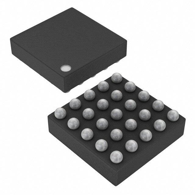
4 0 1.0 Signal/Pin Connection and Description 6 9 N 1.1 CONNECTION DIAGRAMS B S U SI 3/ E/ 0 O L K 6 S A C Q R N9 D2 D1 D0/ A0/ DA DR INT B S 28 27 26 25 24 23 22 U D3 1 21 WR/SK 0 D4 2 2 RD D5 3 19 CS 28-Pin CSP D6 8 CLKOUT 4 1 D7 7 XOUT 5 1 RESET 6 XIN 6 1 AGND 5 MODEO 7 1 8 9 10 11 12 13 14 3 + − D C D 1 V3. D D GN VC GN DE O M USBN9603/4SLB CS 1 28 CLKOUT RD 2 27 XOUT WR/SK 3 26 XIN INTR 4 25 MODE0 DRQ 5 24 MODE1 DACK 6 23 GND A0/ALE/SI 7 28-Pin SO 22 Vcc D0/SO 8 21 GND D1 9 20 D– D2 10 19 D+ D3 11 18 V3.3 D4 12 17 AGND D5 13 16 RESET D6 14 15 D7 USBN9603/4-28M www.national.com 6
U 1.0 Signal/Pin Connection and Description (Continued) S B N 1.2 DETAILED SIGNAL/PIN DESCRIPTIONS 9 6 1.2.1 Power Supply 0 3 / I/O Name Description U S NA Vcc DigitalPowerSupply(V ).Power-onresetisdetectedwhentheinputvoltageisat thesame B CC N levelasGNDandthenraisedtotherequiredV level.Thepower-onresetcausesallregisters cc 9 tobesettotheirresetvalues,theclockgeneratortoberesetandstallstheCLKOUToutputfor 6 214 XIN clock cycles. During this time, no internal register is accessible. 0 4 NA GND Digital Power Supply (GND) NA AGND Analog Power Supply (AGND) NA V3.3 Transceiver 3.3V Voltage Supply.This pin can be used as the internal 3.3V voltage regulator output.Theregulatorisintendedtopoweronlytheinternaltransceiverandoneexternalpull-up. Anexternal1µFde-couplingcapacitorisrequiredonthispin.Thevoltageregulatoroutputisdis- ableduponreset.Whentheinternalvoltageregulatorisleftdisabled,thispinmustbeusedasa 3.3V supply input for the internal transceiver. This is the case during 3.3V operation. 1.2.2 Oscillator, Clock and Reset I/O Name Description NA XIN Crystal Oscillator Input.Input for internal 24 MHz crystal oscillator circuit. A 24 MHz funda- mental crystal may be used. NA XOUT Crystal Oscillator Output O CLKOUT ClockOutput.This programmableclockoutputmaybedisabledand configuredfordifferent speeds via the Clock Configuration register. After a power-on reset and hardware reset (as- sertionofRESET), a4MHzclocksignalisoutput(theremaybeaninitialphasediscontinuity). IntheUSBN9604,ahardwareresetcausesCLKOUTtostallfor214XINclockcycles whilethe internal DLL is synchronized to the external reference clock. I RESET Reset. Activelow,assertionof RESETindicatesa hardwarereset,whichcausesallregisters in the device to revert to their reset values. IntheUSBN9604,thehardwareresetactionisidenticaltoapower-onreset. Signalcondition- ing is provided on this input to allow use of a simple, RC power-on reset circuit. Oscillator Circuit TheXINandXOUTpinsmaybeconnectedtomakea24MHzclosed-loop,crystal-controlledoscillator.Alternately,anex- ternal24MHzclocksourcemaybeusedasthe inputclockforthedevice.Theinternalcrystaloscillatorusesa24MHz fundamental crystal. See Table 1 for typical component values and Figure 1 for the crystal circuit. For a specific crystal, please consult the manufacturer for recommended component values. Ifanexternalclocksourceisused,itisconnectedtoXIN.XOUTshouldremainunconnected.Straycapacitanceandinduc- tanceshouldbekeptaslowaspossibleintheoscillatorcircuit.Tracelengthsshouldbeminimizedbypositioningthecrystal and external components as close as possible to the XIN and XOUT pins. Table 1. Approximate Component Values Component Parameters Values Tolerance Crystal Resonator Resonance Frequency 24 MHz 2500 ppm (max) Type AT-Cut Maximum Serial Resistance 50 Ω Maximum Shunt Capacitance 10 pF Load Capacitance 20 pF Resistor R1 1 MΩ ±5% 7 www.national.com
4 0 1.0 Signal/Pin Connection and Description (Continued) 6 9 N B Component Parameters Values Tolerance S U Resistor R2 0 ΝΑ / 3 0 6 Capacitor C1 15 pF ±20% 9 N B Capacitor C2 15 pF ±20% S U External Elements ChooseC1andC2capacitors(seeFigure1)tomatchthecrystal’sloadcapacitance. TheloadcapacitanceC “seen”by L thecrystaliscomprisedofC1inserieswithC2,andinparallelwiththeparasiticcapacitanceofthecircuit. Theparasitic capacitanceiscausedbythechippackage,boardlayoutandsocket(ifany),andcanvaryfrom0to8pF. Theruleofthumb in choosing these capacitors is: C = (C1*C2)/(C1+C2)+C Parasitic L XIN XTAL C1 R1 XOUT C2 R2 Figure 1. Typical Oscillator Circuit 1.2.3 USB Port I/O Name Description I/O D+ USBD+UpstreamPort.Thispinrequiresanexternal1.5kpull-upto3.3Vtosignalfullspeed operation. I/O D– USB D– Upstream Port 1.2.4 Microprocessor Interface I/O Name Description I MODE1-0 Interface Mode.Each of these pins should be hard-wired to V or GND to select the inter- CC face mode: MODE1-0 = 00. Mode 0: Non-multiplexed parallel interface mode MODE1-0 = 01. Mode 1: Multiplexed parallel interface mode MODE1-0 = 10. Mode 2: MICROWIRE interface mode MODE1-0 = 11. Mode 3: Reserved Note:Mode3alsoselectstheMICROWIREinterfacemodeintheUSBN9602,butthismode should be reserved to preserve compatibility with future devices. I DACK DMAAcknowledge.ThisactivelowsignalisonlyusedifDMAisenabled.IfDMAisnotused, this pin must be tied to V . CC O DRQ DMA Request.This pin is used for DMA request only if DMA is enabled. O INTR Interrupt.The interrupt signal modes (active high, active low or open drain) can be config- ured via the Main Control register. During reset, this signal is TRI-STATE . I CS Chip Select.Active low chip select I RD Read.Active low read strobe, parallel interface www.national.com 8
U 1.0 Signal/Pin Connection and Description (Continued) S B N I WR Write. Active low write strobe, parallel interface 9 6 0 SK MICROWIRE Shift Clock. Mode 2 3 / I A0 A0 Address Bus Line. Mode 0, parallel interface U S ALE Address Latch Enable. Mode 1, parallel interface B N SI MICROWIRE Serial Input.Mode 2 9 6 I/O D0 Data Bus Line D0. Mode 0 0 4 AD0 Address/Data Bus LIne AD0. Mode 1 SO MICROWIRE Serial Output. Mode 2 I/O D1 Data Bus Line D1. Mode 0 AD1 Address/Data Bus Line AD1. Mode 1 I/O D2 Data Bus Line D2. Mode 0 AD2 Address/Data Bus Line AD2. Mode 1 I/O D3 Data Bus Line D3.Mode 0 AD3 Address/Data Bus Line AD3. Mode 1 I/O D4 Data Bus Line D4. Mode 0 AD4 Address/Data Bus Line AD4.Mode 1 I/O D5 Data Bus Line D5.Mode 0 AD5 Address/Data Bus Line AD5. Mode 1 I/O D6 Data Bus Line D6. Mode 0 AD6 Address/Data Bus Line AD6.Mode 1 I/O D7 Data Bus Line D7.Mode 0 AD7 Address/Data Bus Line AD7.Mode 1 9 www.national.com
4 0 2.0 Functional Overview 6 9 N ThedeviceisaUniversalSerialBus(USB)NodecontrollercompatiblewithUSBSpecification,1.0and1.1.Itintegratesonto B asingleICtherequiredUSBtransceiverwitha3.3Vregulator,theSerialInterfaceEngine(SIE),USBendpoint FIFOs,a S versatile(8-bitparallelorserial)interfaceandaclockgenerator.Atotalofsevenendpointpipesaresupported:onebidirec- U tional for the mandatory control EP0 and an additional six for unidirectional endpoints to support USB interrupt, bulk and / 3 isochronousdatatransfers.The8-bitparallelinterfacesupportsmultiplexedandnon-multiplexedstyleCPUaddress/data 0 6 buses.ThesynchronousserialMICROWIREinterfaceallowsadaptingtoCPUswithoutexternaladdress/databuses.Apro- 9 grammable interrupt output scheme allows adapting to different interrupt signaling requirements. N B Refer to Figure 2 for the major functional blocks, described in the following sections. S U 2.1 TRANSCEIVER The device contains a high-speed transceiver which consists of three main functional blocks: — Differential receiver — Single-ended receiver with on-chip voltage reference — Transmitter with on-chip current source. This transceiver meets the performance requirements described in Chapter 7 of the USB Specification, Version 1.1. Tominimizesignalskew,thedifferentialoutputswingsofthetransmitterarewellbalanced.Slew-ratecontrolisusedonthe drivertominimizeradiatednoiseandcrosstalk.ThedriverssupportTRI-STATEoperationtoallowbidirectional,half-duplex operation of the transceiver. Thedifferentialreceiveroperatesoverthecompletecommonmoderange,andhasadelayguaranteedtobelargerthan thatofthesingle-endedreceivers.This avoidspotentialglitchesintheSerialInterfaceEngine(SIE)aftersingle-endedze- ros. Single-endedreceiversarepresentoneachofthetwodatalines.Thesearerequired,inadditiontothedifferentialreceiver,to detectanabsolutevoltagewithaswitchingthresholdbetween0.8Vand2.0V(TTLinputs).ToincreaseV rejection,without cc glitching,avoltagereferencesetsthesingle-endedswitchingreference.Anexternal1.5±5%KΩresistorisrequiredonD+to indicatethatthisisahigh-speednode.Thisresistorshouldbetiedtoavoltagesourcebetween3.0Vand3.6V,andreferenced to the local ground, such as the output provided on pin V3.3. 2.2 VOLTAGE REGULATOR (VREG) Thevoltageregulatorprovides 3.3Vfortheintegratedtransceiverfrom5.0VdevicepowerorUSBbuspower.Thisoutput canbeusedtosupplypowertothe1.5KΩpull-upresistor.Thisoutputmustbedecoupledwitha1µFtantalumcapacitor to ground. It can be disabled under software control to allow using the device in a 3.3V system. 2.3 SERIAL INTERFACE ENGINE (SIE) TheSIEiscomprisedofphysical(PHY)andMediaAccessController(MAC)modules.ThePHYmoduleincludesthedigital- clockrecoverycircuit,adigitalglitchfilter,EndOfPacket(EOP)detectioncircuitry,andbitstuffingandunstuffinglogic.The MAC module includes packet formatting, CRC generation and checking, and endpoint address detection. It provides the necessarycontroltogivetheNAK,ACKandSTALLresponsesasdeterminedbytheEndpointPipeController(EPC)forthe specifiedendpointpipe.TheSIEisalsoresponsiblefordetectingandreportingUSB-specificevents,suchasNodeReset, NodeSuspendandNodeResume.Themoduleoutputsignalstothetransceiverarewellmatched(under1nS)tominimize skew on the USB signals. TheUSBspecificationsassignbitstuffingandunstuffingasthemethodtoensureadequateelectricaltransitionsontheline to enable clock recovery at the receiving end. The bit stuffing block ensures that whenever a string of consecutive 1’s is encountered, a 0 is inserted after every sixth 1 in the data stream. The bit unstuffing logic reverses this process. TheclockrecoveryblockusestheincomingNRZIdatatoextractadataclock(12MHz)froma48MHzinputclock.This inputclockisderivedfroma24MHzoscillatorinconjunctionwithPLLcircuitry(clockdoubler).Thisclockisusedinthedata recoverycircuit.Theoutputofthisblockisbinarydata(decodedfromtheNRZIstream)whichcanbeappropriatelysampled usingtheextracted12MHzclock.ThejitterperformanceandtimingcharacteristicsmeettherequirementssetforthinChap- ter 7 of the USB Specification. www.national.com 10
U 2.0 Functional Overview (Continued) S B N 9 6 CS RD WR/SK DACK DRQ INTR MODE1-0 0 3 / U RESET S D7-0/AD7-0/SO B Microcontroller Interface V N CC (Parallel and Serial) 9 A0/ALE/SI GND 6 0 4 Endpoint/Control FIFOs 24 MHz XIN Oscillator XOUT Control Status PLL x 2 2 6 RX P P 0 E E nt oi p End P1 P5 TX GeCnleorcaktor CLKOUT E E SIE Clock Media Access Controller (MAC) Recovery USB Event Physical Layer Interface (PHY) Detect V3.3 Transceiver VReg AGND D+ D- Upstream Port Figure 2. USBN9603/4 Block Diagram 11 www.national.com
4 0 2.0 Functional Overview (Continued) 6 9 N 2.4 ENDPOINT PIPE CONTROLLER (EPC) B S TheEPCprovidestheinterfaceforUSBfunctionendpoints.Anendpointistheultimatesourceorsinkofdata.Anendpoint U pipefacilitatesthemovementofdatabetweenUSBandmemory,andcompletesthepathbetweentheUSBhostandthe 3/ functionendpoint.AccordingtotheUSBspecification,upto31suchendpointsaresupportedatanygiventime.USBallows 0 atotalof16unidirectionalendpointsforreceiveand16fortransmit.Asthecontrolendpoint0isalwaysbidirectional,the 6 totalnumberis31.Sevenendpointpipeswiththesamefunctionaddressaresupported.SeeFigure3foraschematicdia- 9 N gram of EPC operation. B AUSBfunctionisaUSBdevicethatisabletotransmitandreceiveinformationonthebus.Afunctionmayhaveoneormore S configurations,eachofwhichdefinestheinterfacesthatmakeupthedevice.Eachinterface,inturn,iscomposedofoneor U more endpoints. EachendpointisanaddressableentityonUSBandisrequiredtorespondtoINandOUTtokensfromtheUSBhost(typically aPC).INtokensindicatethatthehosthasrequestedtoreceiveinformationfromanendpoint,andOUTtokensindicatethat it is about to send information to an endpoint. OndetectionofanINtokenaddressedtoanendpoint,theendpointpipeshouldrespondwithadatapacket.Iftheendpoint pipeiscurrentlystalled,aSTALLhandshakepacketissentundersoftwarecontrol.Iftheendpointpipeisenabledbutno dataispresent,aNAK(NegativeAcknowledgment)handshakepacketissentautomatically.Iftheendpointpipeisisochro- nous and enabled but no data is present, a bit stuff error followed by an end of packet is sent on the bus. Similarly,ondetectionofanOUTtokenaddressedtoanendpoint,theendpointpipeshouldreceiveadatapacketsentby thehostandloaditintotheappropriateFIFO.Iftheendpointpipeisstalled,aSTALLhandshakepacketissent.Iftheend- pointpipeisenabledbutnobufferispresentfordatastorage,aNAKhandshakepacketissent.Iftheendpointisisochro- nous and enabled but cannot handle the data, no handshake packet is sent. A disabled endpoint does not respond to IN, OUT, or SETUP tokens. The EPC maintains separate status and control information for each endpoint pipe. ForINtokens,theEPCtransfersdatafromtheassociatedFIFOtothehost.ForOUTtokens,theEPCtransfersdatainthe opposite direction. Control Registers USB Function Address EP0 Compare FIFOs USB SIE DMA Control Endpoint Pipe Controller EPA EPB EPC. Control Registers FIFO Receive Endpoint Pipes Microcontroller Interface EPX EPY EPZ Control Registers FIFO Transmit Endpoint Pipes Figure 3. EPC Operation 2.5 MICROCONTROLLER INTERFACE ThedevicecanbeconnectedtoaCPUormicrocontrollerviathe8-bitparallelorMICROWIREinterface.Theinterfacetype isselectedbytheinputmodepinsMODE0andMODE1.Inaddition,aconfigurableinterruptoutputisprovided.Theinterrupt type can be configured to be either open-drain active-low or push-pull active high or low. www.national.com 12
U 3.0 Parallel Interface S B TheparallelinterfaceallowsthedevicetofunctionasaCPUormicrocontrollerperipheral.Thisinterfacetypeanditsad- N dressing mode (multiplexed or non-multiplexed) is determined via device input pins MODE0 and MODE1. 9 6 0 3.1 NON-MULTIPLEXED MODE 3 / Non-multiplexedmodeusesthecontrolpinsCS,RD,WR,theaddresspinA0andthebidirectionaldatabusD7-0asshown U in Figure 4. This mode is selected by tying both the MODE1 and MODE0 pins to GND. S B N 9 6 0 CS 4 DATA_IN 0x00 A0 Data In WR RD Data Out DATA_OUT D7-0 ADDR Address 0x3F Register File Figure 4. Non-Multiplexed Mode Block Diagram TheCPUhasdirectaccesstotheDATA_IN,DATA_OUTandADDRregisters.Readingandwritingdatatothedevicecan be done either in standard access or burst mode. See Figure 5 for timing information. CS A0 RD WR D7-0 Input Out Out Write Address Read Data Burst Read Data Figure 5. Non-Multiplexed Mode Timing Diagram 13 www.national.com
4 0 3.0 Parallel Interface (Continued) 6 9 N 3.1.1 Standard Access Mode B S Thestandardaccesssequencefornon-multiplexedmodeistowritetheaddresstotheADDRregisterandthenreadorwrite U thedatafrom/totheDATA_OUT/DATA_INregister.TheDATA_OUTregisterisupdatedafterwritingtotheADDRregister. 3/ The ADDR register or the DATA_OUT/DATA_IN register is selected with the A0 input. 0 6 3.1.2 Burst Mode 9 N In burst mode, the ADDR register is written once with the desired memory address of any of the on-chip registers. Then B consecutivereads/writesareperformedtotheDATA_IN/DATA_OUTregisterwithoutpreviouslywritinganewaddress.The S content of the DATA_OUT register for read operations is updated once after every read or write. U 3.1.3 User Registers The following table gives an overview of the parallel interface registers in non-multiplexed mode. The reserved bits return undefined data on read and should be written with 0. A0 Access bit 7 bit 6 bit 5 bit 4 bit 3 bit 2 bit 1 bit 0 0 Read DATA_OUT 0 Write DATA_IN 1 Read Reserved 1 Write Reserved ADDR5-0 Address Register (ADDR) The ADDR register acts as a pointer to the internal memory. This register is write only and is cleared on reset. Data Output Register (DATA_OUT) TheDATA_OUTregisterisupdatedwiththecontentsofthememoryregistertowhichtheADDRregisterispointing.Update occurs under the following conditions: 1. After the ADDR register is written. 2. After a read from the DATA_OUT register. 3. After a write to the DATA_IN register. This register is read only and holds undefined data after reset. Data Input Register (DATA_IN) TheDATA_INregisterholdsthedatawrittentothedeviceaddresstowhichADDRpoints.Thisregisteriswriteonlyandis cleared on reset. www.national.com 14
U 3.0 Parallel Interface (Continued) S B N 3.2 MULTIPLEXED MODE 9 MultiplexedmodeusesthecontrolpinsCS,RD,WR,theaddresslatchenablesignalALEandthebidirectionaladdressdata 6 0 busAD7-0asshowninFigure6.ThismodeisselectedbytyingMODE1toGNDandMODE0toVCC. Theaddressislatched 3 intotheADDRregisterwhenALEishigh.Dataisoutput/inputwiththenextactiveRDorWRsignal.Allregistersaredirectly /U accessible in this interface mode. S B Figure 7 shows basic timing of the interface in Multiplexed mode. N 9 CS 6 Data In 0x00 04 WR RD Data Out AD7-0 ADDR ALE EN Address 0x3F Register File Figure 6. Multiplexed Mode Block Diagram ALE CS RD orWR AD7-0 ADDR DATA Figure 7. Multiplexed Mode Basic Read/Write Timing 15 www.national.com
4 0 4.0 Direct Memory Access (DMA) Support 6 9 N ThedevicesupportsDMAtransferswithanexternalDMAcontrollerfrom/toendpoints1to6.Thismodeusesthedevice B pinsDRQandDACKinadditiontotheparallelinterfacepinsRDorWRandD7-0datapins.DMAmodecanonlybeused S withparallelinterfacemode(MODE1mustbegrounded).Thereadorwriteaddressisgeneratedinternallyandthestateof U the A0/ALE pin is ignored during a DMA cycle. / 3 TheDMAsupportlogichasalowerprioritythantheparallelinterface.CSmuststayinactiveduringaDMAcycle.IfCSbe- 0 6 comesactive,DACKisignoredandaregularread/writeoperationisperformed.Onlyoneendpointcanbeenabledatany 9 given time to issue a DMA request when data is received or transmitted. N B Two different DMA modes are supported: standard and automatic. S U 4.1 STANDARD DMA MODE (DMA) To enable DMA transfers in standard DMA mode, the following steps must be performed: 1. ThelocalCPUprogramstheDMAcontrollerforfly-bydemandmodetransfers.Inthismode,transfersoccuronlywhen thedevicerequeststhemviatheDRQpin.Thedataisread/writtenfrom/tothedevicereceive/transmitFIFOandwrit- ten/read into/from local memory during the same bus transaction. 2. TheDMAaddresscounterisprogrammedtopointtothedestinationmemoryblockinthelocalsharedmemory,andthe ByteCountregisterisprogrammedwiththenumberofbytesintheblocktobetransferred.Ifrequiredtheautomaticerror handlingshouldbeenabledatthispointalongwiththeerrorhandlingcounter.Inadditiontheuserneedstosetthere- spective Endpoint enable bit. 3. The DMA Enable bit and DMA Source bits are set in the DMACNTRL register. 4. TheUSBhostcannowperformUSBbulkorisochronousdatatransfersovertheUSBbustothereceiveFIFOorfrom the transmit FIFO in the device. 5. IftheFIFOswarninglimitisreachedorthetransmission/receptioniscompleted,aDMArequest/acknowledgesequence isinitiatedforthepredeterminednumberofbytes.ThetimeatwhichaDMArequestisissueddependsontheselected DMAmode(controlledbytheDMODbitintheDMACNTRLregister),thecurrentstatusoftheendpointFIFO,andthe FIFO warning enable bits. A DMA request can be issued immediately. 6. AftertheDMAcontrollerhasgrantedcontrolofthebus,itdrivesavalidmemoryaddressandassertsDACKandRDor WR,thustransferringabytefromthe receiveFIFOtomemory,orfrommemorytothetransmitFIFO.Thisprocesscon- tinues until the DMA byte count, within the DMA controller, reaches zero. 7. Aftertheprogrammedamountofdataistransferred,thefirmwaremustdooneofthefollowing(dependingonthetransfer direction and mode): — Queue the new data for transmission by setting the TX_EN bit in the TXCx register. — SettheEndOfPacketmarkerbysettingtheTX_LASTbitintheTXCxregister.Re-enablereceptionbysettingthe RX_EN bit in the RXCx register. — Check if the last byte of the packet was received (RX_LAST bit in the RXSx register). The DMA transfer can be halted at any time by resetting the DMA Request Enable bit. If the DMA Request Enable bit is cleared during the middle of a DMA cycle, the current cycle is completed before the DMA request is terminated. See Figures 8 and 9 for the transmit and receive sequences using standard DMA mode. MIcrocontroller DMA Microcontroller USB DMA time Set up DMA Fill FIFO Enable TX Transaction Fill FIFO Figure 8. Transmit Operation in Standard DMA Mode Microcontroller Microcontroller USB DMA Microcontroller time Set up DMA Enable RX Transaction Read FIFO Enable RX Figure 9. Receive Operation in Standard DMA Mode www.national.com 16
U 4.0 Direct Memory Access (DMA) Support (Continued) S B N 4.2 AUTOMATIC DMA MODE (ADMA) 9 TheADMAmodeallowstheCPUtotransferindependentlylargebulkorisochronousdatastreamstoorfromtheUSBbus. 6 0 Theapplication’sDMAcontroller,togetherwiththeADMAlogic,havethecapabilitytosplitalargeamountofdataandtrans- 3 feritin(FIFOsize)packetsviatheUSB.Inaddition,automaticerrorhandlingisperformedinordertominimizefirmware /U intervention.Thenumberoftransferreddatastreambytesmustbeofamodulo64size.Themaximumamountofdatais S restricted to 256*64 bytes = 16 Kbytes. B N To enable an ADMA transfer, the following steps must be performed: 9 1. ThelocalCPUprogramstheDMAcontrollerforfly-bydemandmodetransfers.Inthismode,transfersoccuronlyinre- 6 0 sponsetoDMArequestviatheDRQpin.Thedataisread/writtenfrom/tothereceive/transmitFIFOandwritten/readin- 4 to/from local memory during the same bus transaction. 2. TheDMAaddresscounterisprogrammedtopointtothedestinationmemoryblockinthelocalsharedmemory,andthe ByteCountregisterisprogrammedwiththenumberofbytesintheblocktobetransferred.TheDMACountregistermust beconfiguredwiththenumberofpacketstobereceivedortransmitted. Ifrequired,theAutomaticErrorHandlingregister must also be configured at this time. 3. The ADMA enable bit must be set prior to, or at the same time as the DMA enable bit. The DMA enable bit must be cleared before enabling ADMA mode. 4. TheDMARequestEnablebitandDMASourcebitsaresetinthedevice.TherespectiveendpointEnablebitmustalso be set. 5. TheUSBhostcannowperformUSBbulkorisochronousdatatransfersovertheUSBbustothereceiveFIFOorfrom thetransmitFIFO.Steps5to7ofthenormalDMAmodeareperfromedautomatically.TheADMAisstoppedeitherwhen the last packet is received or when the DMA Count register has reached the value zero. SeeFigures10and11forthetransmitandreceivesequencesusingADMAmode. SeeFigures12and13forthebasic DMA write timing and read timing. Microcontroller DMA USB DMA USB USB Set up ADMA Fill FIFO Transaction Fill FIFO Transaction Last time Transaction Figure 10. Transmit Operation Using ADMA Mode Microcontroller USB DMA USB DMA DMA Set up ADMA Transaction Read FIFO Transaction Read FIFO Last time Read FIFO Figure 11. Receive Operation Using ADMA Mode 17 www.national.com
4 0 4.0 Direct Memory Access (DMA) Support (Continued) 6 9 N B S U / 3 DRQ 0 6 9 N B DACK S U WR D7-0 Input Figure 12. DMA Write to USBN9603/4 DRQ DACK RD D7-0 Output Figure 13. DMA Read from USBN9603/4 www.national.com 18
U 5.0 MICROWIRE/PLUS Interface S B TheMICROWIRE/PLUSinterfaceallowsthedevicetofunctionasaCPUormicrocontrollerperipheralviaaserialinterface. N ThismodeisselectedbypullingtheMODE1pinhighandtheMODE0pinlow.TheMICROWIRE/PLUSmodeusesthechip 9 select (CS), serial clock (SK), serial data in (SI) and serial data out (SO) pins, as shown in Figure 14. 6 0 3 / U S 0x00 B Data Out N SK SYNC 9 6 DATA_OUT 0 4 CS SO SHIFT SI Data In DATA_IN ADDR Address 0x3F CMD1-0 Register File Figure 14. MICROWIRE/PLUS Interface Block Diagram 5.1 OPERATING COMMANDS TheMICROWIRE/PLUSinterfaceisenabledbyafallingedgeofCSandresetwitharisingedgeofCS.DataonSIisshifted in after the rising edge of SK. Data is shifted out on SO after the falling edge of SK. Data is transferred from/to the Shift registerafterthefallingedgeoftheeighthSKclock.Dataistransferredwiththemostsignificantbitfirst.Table2summarizes the available commands (CMD) for the MICROWIRE/PLUS interface. Note:Awriteoperationtoanyregisteralwaysreadsthecontentsoftheregisterafterthewritehasoccurred,andshiftsout thatdatainthenextcycle.Thisreaddoesnotclearthebitintherespectiveregisters,evenforaClearonRead(CoR)type bit,withoneexception:writingtotheTXDx(transmitdata)registers,whichcausesundefineddatatobereadduringthenext cycle. Table 2. Command/Address Byte Format Byte Transferred Sequence Initiated1 CMD ADDR Cycle Description 1 0 5 4 3 2 1 0 0 0 RADDR 1 Shift in CMD/RADDR; shift out previous read data (read) 2 Shift in next CMD/ADDR; shift out RADDR data 0 1 x 1 noaction;shiftoutpreviousreaddata(donotclearCoRbits) 1 0 WADDR 1 Shift in CMD/WADDR; shift out previous read data (normal write) 2 Shift in WADDR write data; shift out WADDR read data (do not clear CoR bits) 1 1 WADDR 1 Shift in CMD/WADDR; shift out previous read data (burst write) 2-n Shift in WADDR write data; shift out WADDR read data (do not clear CoR bits); terminate this mode by pulling CS high 1. 1 cycle = 8 SK clocks. Data is transferred after the 8th SK of 1 cycle. 19 www.national.com
4 0 5.0 MICROWIRE/PLUS Interface (Continued) 6 9 N 5.2 READ AND WRITE TIMING B S Dataisreadbyshiftinginthe2-bitcommand(CMDandthe6-bitaddress,RADDRorWADDR)whilesimultaneouslyshifting U out read data from the previous address. / 3 Datacanbewritteninstandardorburstmode.Standardmoderequirestwobytes:onebyteforthecommandandaddress 0 tobeshiftedin,andonebytefordatatobeshiftedin.Inburstmode,thecommandandaddressaretransferredfirst,and 6 9 then consecutive data is written to that address. Burst mode is terminated whenCS becomes inactive (high). N B See Figure 15 for basic read timing, Figure 16 for standard write timing, and Figure 17 for write timing in burst mode. S U CS SK 8 Cycles 8 Cycles 8 Cycles SI CMD = 0x ADDR CMD = 0x ADDR New Command SO Undefined Data Read Data Read Data Figure 15. Basic Read Timing CS SK 8 Cycles 8 Cycles 8 Cycles SI CMD = 10 ADDR Write Data New Command SO Undefined Data Read Data Read Data Figure 16. Standard Write Timing www.national.com 20
U 5.0 MICROWIRE/PLUS Interface (Continued) S B N 9 6 0 CS 3 / U S B N 9 6 SK 8 Cycles 8 Cycles 8 Cycles 0 4 SI CMD=11 ADDR Write Data Write Data SO Undefined Data Read Data Read Data Figure 17. Burst Write Timing 21 www.national.com
4 0 6.0 Functional Description 6 9 N 6.1 FUNCTIONAL STATES B S 6.1.1 Line Condition Detection U At any given time, the device is in one of the following states (see Section 6.1.2 for the functional state transitions): / 3 0 • NodeOperational Normal operation 6 9 • N NodeSuspend Device operation suspended due to USB inactivity B • S NodeResume Device wake-up from suspended state U • NodeReset Device reset The NodeSuspend, NodeResume, or NodeReset line condition causes a transition from one operating state to another. TheseconditionsaredetectedbyspecializedhardwareandreportedviatheAlternateEvent(ALTEV)register.Ifinterrupts are enabled, an interrupt is generated upon the occurrence of any of the specified conditions. NodeOperational This is the normal operating state of the device. In this state, the node is configured for operation on the USB bus. NodeSuspend AUSBdeviceisexpectedtoenterNodeSuspendstatewhen3mShaveelapsedwithoutanydetectablebusactivity.The device looksforthiseventandsignalsitbysettingtheSD3bitintheALTEVregister,whichcausesaninterrupt,ifenabled, to be generated. The firmware should respond by putting the device into the NodeSuspend state. Thedevicecanresumenormaloperationunderfirmwarecontrolinresponsetoalocaleventatthehostcontroller.Itcan wakeuptheUSBbusviaaNodeResume,orwhendetectingaresumecommandontheUSBbus,whichsignalsaninterrupt to the host controller. NodeResume If the host has enabled remote wake-ups from the node, the device can initiate a remote wake-up. Oncethefirmwaredetectstheevent,whichwakesupthebus,itreleasesthedevicefromNodeSuspendstatebyinitiating a NodeResume on the USB using the NFSR register. The node firmware must ensure at least 5 mS of Idle on the USB. WhileinNodeResumestate,aconstant“K”issignalledontheUSB.Thisshouldlastforatleast1mSandnomorethan5 mS,afterwhichtheUSBhostshouldcontinuesendingtheNodeResumesignalforatleastanadditional20mS,andthen completes the NodeResume operation by issuing the End Of Packet (EOP) sequence. To successfully detect the EOP, the firmware must enter USB NodeOperational state by setting the NFSR register. If no EOP is received from the host within 100 mS, the software must reinitiate NodeResume. NodeReset WhendetectingaNodeResumeorNodeResetsignalwhileinNodeSuspendstate,thedevicecansignalthistothemain controller by generating an interrupt. USB specifications require that a device must be ready to respond to USB tokens within 10 mS after wake-up or reset. 6.1.2 Functional State Transition Figure18showsthedevicestatesandtransitions,aswellas theconditionsthattriggereachtransition.Allstatetransitions are initiated by the firmware. www.national.com 22
U 6.0 Functional Description (Continued) S B N 9 6 0 set_oper 3 NodeOperational /U 10b S hw/swreset suspend_det & B set_suspend reset_det &set_reset N 9 6 NodeReset 0 4 00b resume_compl & set_oper resume_det & set_oper NodeResume 01b NodeSuspend 11b local_event & sd5_detect & clear_suspend reset_det &set_reset Bold Italics =Transition initiated by firmware Notes: 1. WhenthenodeisnotinNodeOperationalstate,allregistersarefrozenwiththeexceptionoftheendpointcon- troller state machines, and the TX_EN, LAST and RX_EN bits which are reset. 1. In NodeResume state, resume signaling is propagated upstream. 2. In NodeSuspend state, the node may enter a low power state and is able to detect resume signaling. Figure 18. Node Functional State Diagram Table 3. Functional States State Condition Asserted Transition Node Functional State register NFS[1:0] bits are written with 00 set_reset b The firmware should only initiate set_reset if RESET in the ALTEV register is set. Node Functional State register NFS[1:0] bits are written with 11 set_suspend b The firmware should only initiate set_suspend if SD3 in the ALTEV register is set. set_oper Node Functional State register NFS[1:0] bits are written with 10b Node Functional State register NFS[1:0] bits are written with 01 clear_suspend b The firmware should only initiate clear_suspend if SD5 in the ALTEV register is set. reset_det RESET in the ALTEV register is set to 1 local_event A local event that should wake up the USB. sd5_det SD5 in the ALTEV register is set to 1. suspend_det SD3 in the ALTEV register is set to 1. resume_det RESUME in the ALTEV register is set to1. The node should stay in NodeResume state for at least 10mS and then must enter resume_compl USBOperationalstatetodetecttheEOPfromthehost,whichterminatesthisRemote Resume operation. EOP is signalled when EOP in the ALTEV register is set to 1. 23 www.national.com
4 0 6.0 Functional Description (Continued) 6 9 N 6.2 ENDPOINT OPERATION B S 6.2.1 Address Detection U / PacketsarebroadcastfromthehostcontrollertoallthenodesontheUSBnetwork.Addressdetectionisimplementedin 3 0 hardwaretoallowselectivereceptionofpacketsandtopermitoptimaluseofmicrocontrollerbandwidth.Onefunctionad- 6 dresswithsevendifferentendpointcombinationsisdecodedinparallel.Ifamatchisfound,thenthatparticularpacketis 9 N received into the FIFO; otherwise it is ignored. B TheincomingUSBPacketAddressfieldandEndpointfieldareextractedfromtheincomingbitstream.Thentheaddress S fieldiscomparedtotheFunctionAddressregister(FADR).Ifamatchisdetected,theEndpointfieldiscomparedtoallof U theEndpointControlregisters(EPCx)inparallel.Amatchthencausesthepayloaddatatobereceivedortransmittedusing the respective endpoint FIFO. ADDR Field Endpoint Field - USB Packet - match FADR Register match Receive/Transmit FIFO0 EPC0 Register Transmit FIFO1 EPC1 Register Receive FIFO1 EPC2 Register Transmit FIFO2 EPC3 Register Receive FIFO2 EPC4 Register Transmit FIFO3 EPC5 Register Receive FIFO3 EPC6 Register Figure 19. USB Function Address/Endpoint Decoding 6.2.2 Transmit and Receive Endpoint FIFOs ThedeviceusesatotalofseventransmitandreceiveFIFOs:onebidirectionaltransmitandreceiveFIFOforthemandatory controlendpoint,threetransmitFIFOsandthreereceiveFIFOs.AsshowninTable 4,thebidirectionalFIFOforthecontrol endpointis8bytesdeep.TheadditionalunidirectionalFIFOsare64byteseachforbothtransmitandreceive.EachFIFO canbeprogrammedforoneexclusiveUSBendpoint,usedtogetherwithonegloballydecodedUSBfunctionaddress.The firmware must not enable both transmit and receive FIFOs for endpoint zero at any given time. www.national.com 24
U 6.0 Functional Description (Continued) S B N Table 4. USBN9603/4 Endpoint FIFO Sizes 9 6 0 TX FIFO RX FIFO 3 Endpoint No. / U Size (Bytes) Name Size (Bytes) Name S B 0 8 FIFO0 N 9 1 64 TXFIFO1 6 0 2 64 RXFIFO1 4 3 64 TXFIFO2 4 64 RXFIFO2 5 64 TXFIFO3 6 64 RXFIFO3 Iftwoendpointsinthesamedirectionareprogrammedwiththesameendpointnumberandbothareenabled,dataisre- ceivedortransmittedto/fromtheendpointwiththelowernumber,untilthatendpointisdisabledforbulkorinterrupttransfers, orbecomesfulloremptyforISOtransfers.Forexample,ifreceiveEP2andreceiveEP4bothuseendpoint5andareboth isochronous,thefirstOUTpacketisreceivedintoEP2andthesecondOUTpacketintoEP4,assumingnofirmwareinter- actioninbetween.ForISOendpoints,thisallowsimplementingaping-pongbufferschemetogetherwiththeframenumber match logic. Endpoints in different directions programmed with the same endpoint number operate independently. Bidirectional Control Endpoint FIFO0 Operation FIFO0 should be used for the bidirectional control endpoint zero. It can be configured to receive data sent to the default address with the DEF bit in the EPC0 register. Isochronous transfers are not supported for the control endpoint. The Endpoint 0 FIFO can hold a single receive or transmit packet with up to 8 bytes of data. Figure 20 shows the basic operation in both receive and transmit direction. Note: The actual current operating state is not directly visible to the user. FLUSH Bit TXC0 Register FLUSH Bit, RXC0 Register IDLE RX_EN Bit, RXC0 Register Write to TXD0 TXFILL RXWAIT SETUP Token TX_EN Bit, TXC0 Register (*) OUT or SETUP Token Transmission TXWAIT Done FIFO0 Empty (All Data Read) IN token RX TX (*) For zero length packet, TX_EN causes a transition from IDLE to TXWAIT Figure 20. Endpoint 0 Operation 25 www.national.com
4 0 6.0 Functional Description (Continued) 6 9 N ApacketwrittentotheFIFOistransmittedifanINtokenfortherespectiveendpointisreceived.Ifanerrorconditionisde- B tected, the packet data remains in the FIFO and transmission is retried with the next IN token. S U TheFIFOcontentscanbeflushedtoallowresponsetoanOUTtokenortowritenewdataintotheFIFOforthenextINtoken. / 3 IfanOUTtokenisreceivedfortheFIFO,thefirmwareisinformedthattheFIFOhasreceiveddataonlyiftherewasnoerror 0 condition (CRC or STUFF error). Erroneous receptions are automatically discarded. 6 9 N Transmit Endpoint FIFO Operation (TXFIFO1, TXFIFO2, TXFIFO3) B S TheTransmitFIFOsforEndpoints1,3and5supportbulk,interruptandisochronousUSBpackettransferslargerthanthe U actualFIFOsize.Therefore.thefirmwaremustupdatetheFIFOcontentswhiletheUSBpacketistransmittedonthebus. Figure 21 illustrates the operation of the transmit FIFOs. FLUSH (Resets TXRP and TXWP) TXRP TFxS - 1 0x0 + TXFL = TXWP - TXRP + Tx FIFO X TXWP + TCOUNT = TXRP - TXWP (= TFxS - TXFL) Figure 21. Tx FIFO Operation TFxS Transmit FIFO x Size. This is the total number of bytes available within the FIFO. TXRP TransmitReadPointer.ThispointerisincrementedeverytimetheEndpointControllerreadsfromthetransmitFIFO.This pointer wraps around to zero if TFxS is reached. TXRP is never incremented beyond the value of the write pointer TXWP. AnunderrunconditionoccursifTXRPequalsTXWPandanattemptismadetotransmitmorebyteswhentheLASTbitin the TXCMDx register is not set. TXWP TransmitWritePointer.ThispointerisincrementedeverytimethefirmwarewritestothetransmitFIFO.Thispointerwraps around to zero if TFxS is reached. IfanattemptismadetowritemorebytestotheFIFOthanactualspaceavailable(FIFOoverrun),thewritetotheFIFOis ignored. If so, TCOUNT is checked for an indication of the number of empty bytes remaining. TXFL Transmit FIFO Level. This value indicates how many bytes are currently in the FIFO. AFIFOwarningisissuedifTXFLdecreasestoaspecificvalue.TherespectiveWARNxbitintheFWRregisterissetifTXFL is equal to or less than the number specified by the TFWL bit in the TXCx register. www.national.com 26
U 6.0 Functional Description (Continued) S B N TCOUNT 9 TransmitFIFOCount.ThisvalueindicateshowmanyemptybytescanbefilledwithinthetransmitFIFO.Thisvalueisac- 6 0 cessible by firmware via the TxSx register. 3 / U S Receive Endpoint FIFO Operation (RXFIFO1, RXFIFO2, RXFIFO3) B N TheReceiveFIFOsfortheEndpoints2,4and6supportbulk,interruptandisochronousUSBpackettransferslargerthan 9 theactualFIFOsize.IfthepacketlengthexceedstheFIFOsize,thefirmwaremustreadtheFIFOcontentswhiletheUSB 6 0 packet is being received on the bus. Figure 22 shows the detailed behavior of receive FIFOs. 4 FLUSH (Resets RXRP and RXWP) RXRP RFxS - 1 0x0 RCOUNT = RXWP - RXRP + + Rx FIFO X RXWP + RXFL = RXRP - RXWP (= RFxS - RCOUNT) Figure 22. Rx FIFO Operation RFxS Receive FIFO x Size. This is the total number of bytes available within the FIFO. RXRP ReceiveReadPointer.ThispointerisincrementedwitheveryreadofthefirmwarefromthereceiveFIFO.Thispointerwraps around to zero if RFxS is reached. RXRP is never incremented beyond the value of RXWP. If an attempt is made to read more bytes than are actually available (FIFO underrun), the last byte is read repeatedly. RXWP ReceiveWritePointer.ThispointerisincrementedeverytimetheEndpointControllerwritestothereceiveFIFO.Thispointer wraps around to zero if RFxS is reached. An overrun condition occurs if RXRP equals RXWP and an attempt is made to write an additional byte. RXFL ReceiveFIFOLevel.Thisvalueindicateshowmanymorebytescanbereceiveduntilanoverrunconditionoccurswiththe next write to the FIFO. AFIFOwarningisissuedifRXFLdecreasestoaspecificvalue.TherespectiveWARNxbitintheFWRregisterissetifRXFL is equal to or less than the number specified by the RFWL bit in the RXCx register. RCOUNT ReceiveFIFOCount.ThisvalueindicateshowmanybytescanbereadfromthereceiveFIFO.Thisvalueisaccessibleby firmware via the RXSx register. 27 www.national.com
4 0 6.0 Functional Description (Continued) 6 9 N 6.2.3 Programming Model B S Figure 23 illustrates the register hierarchy for event reporting. U . / 3 0 6 MAEV 9 N B S U FWEV RXEV TXEV ALTEV NAKEV TXS0 TXC0 TXD0 EPC0 RXS0 FIFO0 RXC0 8 byte RXD0 TXSx EPCx TXCx TFIFOx 64 byte TXDx RXSy EPCy RXCx RFIFOy 64 byte RXDy Figure 23. Register Hierarchy 6.3 POWER SAVING MODES TominimizethepowerconsumptionoftheUSBnode,thedevicecanbesettoastaticHaltmode.DuringHaltmode,the clockoscillatorcircuitisdisabled,stoppingtheexternal24MHzclockand48MHzfrequencydoubler,aswellastheclock output signal provided on the CLKOUT pin. However, all device internal status and register settings are preserved. The device is set to Halt mode under the following conditions: (cid:1) If Halt On Suspend (HOS) is enabled (the HOS bit in the WKUP register is set to 1), the device enters Halt mode when the node is set in Suspend state. Writing a 1 to HOS after the node is in Suspend state has no effect. (cid:1) If the node is not attached, the device enters Halt mode, when the Force Halt bit (FHT) in the Wake-Up register is set to 1. www.national.com 28
U 6.0 Functional Description (Continued) S B N 9 6 Power-On Reset 0 External RESET 214 cycles 3/ U Power-Up S Delay B Power-Up Delay N Timeout 9 Wake-Up 6 Event 0 4 Halt Active Halt On Suspend or Force Halt Figure 24. Power Saving Modes The device exits Halt mode in response to one of the following wake-up events: (cid:1) A high-to-low transition is detected on the CS pin and the wake-up Enable bit, ENUC in the WKUP register, is set to 1. (cid:1) Any activity on the USB is detected (USB not idle) and the wake-up Enable bit, ENUSB in the WKUP register is set to 1. (The node can detect any USB activity only when it is attached.) Whenavalidwake-upeventisdetected,thedevicereturnstoactivemodeafterapower-updelayof214XINclockcycles haselapsed(approximately680usec).Thisdelayisestablishedbya14-bitdelaycounter,whichensuresthatthe24MHz oscillatorhasreachedastableconditionandtheclockdoublerlocksandgeneratesastable48MHzsignal.Afterthisstart- up delay, the clock signal can be output on the CLKOUT pin. 6.4 CLOCK GENERATION The Clock Generator provides the CLKOUT output signal based on the programming of the Clock Configuration register (CCONF).Thisallowsdisablingoftheoutputclockandselectionofaclockdivisor.Theclockdivisorsupportsaprogram- mableoutputintherangeof48MHzto2.82MHz.Onapower-onreset,theoutputclockdefaultsto4MHz.Asoftwarereset has no effect on the programming of the CCONF, and thus no effect on the CLKOUT signal. TheonlydifferencebetweentheUSBN9603and USBN9604devicesistheeffectofahardwareresetontheclockgener- ationcircuit. IntheUSBN9604,assertionoftheRESETinputcausestheclockgenerationcircuittobereset,whereasinthe USBN9603, the clock generation circuit is not reset. IntheUSBN9603,however,assertionoftheRESETinputdoescauseallregisterstoreverttotheirresetvalues,including CCONF, which then forces the CLKOUT signal to its default of 4 MHz. IntheUSBN9604,assertionoftheRESETinputcausestheclockgenerationcircuittoberesetaswiththepower-onreset. Aspartoftheclockgenerationreset,adelayof 214XINclockcyclesisincurredbeforetheCLKOUTsignalisoutput.As- sertionoftheRESETinputalsocausesallregisterstoreverttotheirresetvalues,including CCONF,whichthenforcesthe CLKOUT signal to its default of 4 MHz. Thisdifferenceisparticularlyimportantforbus-poweredoperations.Insuchapplications,thevoltageprovidedbythebus mayfallbelowacceptablelevelsfortheclockgenerationcircuit.Whenthisoccurs,aresetmustbeappliedtothiscircuitto guaranteeproperoperation.Afteradelayof214XINclockcycles,theCLKOUTsignalisoutput. Thislowvoltagedetection istypicallyaccomplishedinbus-poweredapplicationsusingavoltagesensor,suchastheLP3470,toappropriatelyreset the CPU and other components, including the USBN9604. Inself-poweredapplicationswherethereisdirectcontroloverthevoltagesupply,thereisnoneedfortheRESETinputto causetheclockgenerationcircuitrytoberesetandthe CLKOUTsignaltostallfor 214XINclockcycles.TheUSBN9603is thus suited for self-powered applications that use the CLKOUT signal as a system clock. 29 www.national.com
4 0 7.0 Register Set 6 9 N Thedevicehasasetofmemory-mappedregistersthatcanbereadfrom/writtentocontroltheUSBinterface.Someregister B bits are reserved; reading from these bits returns undefined data. Reserved register bits should always be written with 0. S The following conventions are used to describe the register format: U / 3 Bit Number bit 7 bit 6 bit 5 bit 4 bit 3 bit 2 bit 1 bit 0 0 6 9 Bit Mnemonic Abbreviated bit/field names N B Corresponding FIFO Corresponding FIFO types and numbers, where relevant S U Reset Value reset values, where relevant r = Read only w = Write only r/w = Read and write by firmware Register Type CoR = Cleared on read CoW = Cleared on write if written with 0; writing a 1 has no effect HW = Modified by the device and by firmware 7.1 CONTROL REGISTERS 7.1.1 Main Control Register (MCNTRL) bit 7 bit 6 bit 5 bit 4 bit 3 bit 2 bit 1 bit 0 INTOC1-0 Reserved NAT VGE Reserved SRST 0 0 - 0 0 0 r/w - r/w r/w r/w SRST SoftwareReset.Settingthisbitcausesasoftwareresetofthedevice.Thisresetisequivalenttoahardwareresetexcept thattheClockConfiguration(CCONF)registerisunaffected.Allregistersreverttotheirdefaultvalues.Thisbitiscleared automatically upon completion of the initiated reset. VGE VoltageRegulatorEnable.Settingthisbitenablestheinternal3.3Vvoltageregulator.Thisbitishardwareresetonlytoa0, disablingtheinternal3.3Vregulatorbydefault.Whentheinternal3.3Vregulatorisdisabled,thedeviceiseffectivelydiscon- nectedfromUSB.Uponpower-up,thefirmwaremayperformanyneededinitialization(suchaspower-onselftest)andthen set the VGE bit. Until the VGE bit is set, the upstream hub port does not detect the device presence. If the VGE bit is reset an external 3.3V power supply may be used on the V3.3 pin. NAT Node Attached. This bit indicates that this node is ready to be detected as attached to USB. When reset the transceiver forcesSE0ontheUSBporttopreventthehub(towhichthisnodeisconnectedto)fromdetectinganattachevent.After reset,thisbitisleftclearedtogivethedevicetimebeforeitmustrespondtocommands.Afterthisbitisset,thedeviceno longer drives the USB and should be ready to receive Reset signaling from the hub. TheNATbitshouldbesetbythefirmwareifanexternal3.3VsupplyhasbeenprovidedtotheV3.3pin,oratleast1mS after the VGE bit is set (in the latter case, the delay allows the internal regulator sufficient time to stabilize). INTOC Interrupt Output Control. These bits control interrupt ouput according to the following table. www.national.com 30
U 7.0 Register Set (Continued) S B N Table 5. Interrupt Output Control Bits 9 6 0 INTOC 3 Interrupt Output / U 1 0 S B 0 0 Disabled N 9 0 1 Active low open drain 6 0 1 0 Active high push-pull 4 1 1 Active low push-pull 7.1.2 Clock Configuration Register (CCONF) bit 7 bit 6 bit 5 bit 4 bit 3 bit 2 bit 1 bit 0 CODIS Reserved CLKDIV3-0 0 - 1 0 1 1 r/w - r/w CLKDIV ExternalClockDivisor.Thepower-onresetandahardwareresetconfigurethedivisorto11 (decimalformat),whichyields d a 4 MHz output clock. frequency = 48 MHz / (CLKDIV+1) IftheCLKDIVvalueischangedbyfirmware,theclockoutputisexpanded/shortenediftheCLKDIVvalueisincreased/de- creased in its current phase, to allow glitch-free switching at the CLKOUT pin. CODIS ClockOutputDisable.Settingthisbitdisablestheclockoutput.TheCLKOUToutputsignalisfrozeninitscurrentstateand resumes with a new period when this bit is cleared. 7.1.3 Revision Identifier (RID) This register holds the binary encoded chip revision. bit 7 bit 6 bit 5 bit 4 bit 3 bit 2 bit 1 bit 0 Reserved REVID3-0 - 0 0 1 0 - r REVID Revision Identification. For revision 9603 Rev A and 9604 Rev A, the field contains 0010 . b 31 www.national.com
4 0 7.0 Register Set (Continued) 6 9 N 7.1.4 Node Functional State Register (NFSR) B S bit 7 bit 6 bit 5 bit 4 bit 3 bit 2 bit 1 bit 0 U / 3 Reserved NFS1-0 0 6 - 0 0 9 N - r/w B S U NFS NodeFunctionalState.Thefirmwareshouldinitiateallrequiredstatetransitionsaccordingtotherespectivestatusbitsin theAlternateEvent(ALTEV)register.ThevalidtransitionsareshowninFigure18.Thenodefunctionalstatebitssetthe node state, as shown in Table 6. Table 6. USB Functional States NFS Node State Description 1 0 0 0 NodeReset This is the USB Reset state. This is entered upon a module resetorbysoftwareupondetectionofaUSBReset.Uponentry, all endpoint pipes are disabled. DEF in the Endpoint Control 0 (EPC0) register and AD_EN in the Function Address (FAR) register should be cleared by software on entry to this state. On exit, DEF should be reset so the device responds to the default address. 0 1 NodeResume In this state, resume "K" signalling is generated. This state should be entered by firmware to initiate a remote wake-up sequence by the device. The node must remain in this state for at least 1 mS and no more than 15 mS. 1 0 NodeOperational This is the normal operational state. In this state the node is configured for operation on the USB bus. 1 1 NodeSuspend Suspend state should be entered by firmware on detection of a Suspend event while in Operational state. While in Suspend state,thetransceiversoperateintheirlow-powersuspendmode. All endpoint controllers and the bits TX_EN, LAST and RX_EN are reset, while allother internal states are frozen. On detection of bus activity, the RESUME bit in the ALTEV register is set. In response, software can cause entry to NodeOperational state. 7.1.5 Main Event Register (MAEV) bit 7 bit 6 bit 5 bit 4 bit 3 bit 2 bit 1 bit 0 INTR RX_EV ULD NAK FRAME TX_EV ALT WARN 0 0 0 0 0 0 0 0 see text r CoR r CoR r r r WARN OneoftheunmaskedbitsintheFIFOWarningEvent(FWEV)registerhasbeenset.ThisbitisclearedbyreadingtheFWEV register. ALT Alternate. One of the unmasked ALTEV register bits has been set. This bit is cleared by reading the ALTEV register. www.national.com 32
U 7.0 Register Set (Continued) S B N TX_EV 9 TransmitEvent.ThisbitissetifanyoftheunmaskedbitsintheTransmitEvent(TXEV)register(TXFIFOxorTXUNDRNx) 6 0 isset.Therefore,itindicatesthatanINtransactionhasbeencompleted.ThisbitisclearedwhenalltheTX_DONEbitsand 3 the TXUNDRN bits in each Transmit Status (TXSx) register are cleared. / U S FRAME B Thisbitissetiftheframecounterisupdatedwithanewvalue.ThiscanbeduetoreceiptofavalidSOFpacketontheUSB N ortoanartificialupdateiftheframecounterwasunlockedoraframewasmissed.Thisbitisclearedwhentheregisteris 9 6 read. 0 4 NAK NegativeAcknowledge.OneoftheunmaskedNAKEvent(NAKEV)registerbitshasbeenset.Thisbitisclearedwhenthe NAKEV register is read. ULD UnlockLockedDetected.Theframetimerhaseitherenteredunlockedconditionfromalockedcondition,orhasre-entered alockedconditionfromanunlockedconditionasdeterminedbytheULbitintheFrameNumber(FNHorFNL)registerthat is set. This bit is cleared when the register is read. RX_EV Receive Event. This bit is set if any of the unmasked bits in the Receive Event (RXEV) register is set. It indicates that a SETUPorOUTtransactionhasbeencompleted.ThisbitisclearedwhenalloftheRX_LASTbitsineachReceiveStatus (RXSx) register and all RXOVRRN bits in the RXEV register are cleared. INTR MasterInterruptEnable.Thisbitishardwiredto0intheMainEvent(MAEV)register;thecorrespondingbitintheMainMask (MAMSK) register is the Master Interrupt Enable. 7.1.6 Main Mask Register (MAMSK) Whensetto1,aninterruptisenabledwhentherespectiveeventintheMAEVregisterisenabled.Otherwise,interruptgen- eration is disabled. bit 7 bit 6 bit 5 bit 4 bit 3 bit 2 bit 1 bit 0 Same Bit Definition as MAEV Register 0 0 0 0 0 0 0 0 r/w 7.1.7 Alternate Event Register (ALTEV) bit 7 bit 6 bit 5 bit 4 bit 3 bit 2 bit 1 bit 0 RESUME RESET SD5 SD3 EOP DMA WKUP res 0 0 0 0 0 0 0 - CoR CoR CoR CoR CoR r r - WKUP Wake-UpEvent.Thisbitissetwhenawake-upinterruptisgeneratedandissuedontheexternalINTRpin.TheWKUPbit is read only and cleared when the corresponding wake-up pending bit (PNDUC and/or PNDUSB in the Wake-Up (WKUP) register) is cleared. DMA DMA Event. One of the unmasked bits in the DMA Event (DMAEV) register has been set. The DMA bit is read only and cleared when the DMAEV register is cleared. 33 www.national.com
4 0 7.0 Register Set (Continued) 6 9 N EOP B S End of Packet. A valid EOP sequence was detected on the USB. It is used when this device has initiated a Remote wake-up U sequencetoindicatethattheResumesequencehasbeenacknowledgedandcompletedbythehost.Thisbitisclearedwhen / 3 the register is read. 0 6 9 SD3 N SuspendDetect3mS.Thisbitissetafter3mSofIDLEisdetectedontheupstreamport,indicatingthatthedeviceshould B besuspended.ThesuspendoccursunderfirmwarecontrolbywritingthesuspendvaluetotheNodeFunctionalState(NF- S U SR) register. This bit is cleared when the register is read. SD5 SuspendDetect5mS.Thisbitissetafter5mSofIDLEisdetectedontheupstreamport,indicatingthatthisdeviceisper- mittedtoperformaremotewake-upoperation.Theresumemaybeinitiatedunderfirmwarecontrolbywritingtheresume value to the NFSR register. This bit is cleared when the register is read. RESET Thisbitissetwhen2.5µSofSEOisdetectedontheupstreamport.Inresponse,thefunctionalstateshouldbereset(NFS intheNFSRregisterissettoRESET),whereitmustremainforatleast100µS.ThefunctionalstatecanthenreturntoOp- erational state. This bit is cleared when the register is read. RESUME ResumesignallingisdetectedonUSBwhenthedeviceisinSuspendstate(NFSintheNFSRregisterissettoSUSPEND), andanonIDLEsignalispresentonUSB,indicatingthatthisdeviceshouldbeginitswake-upsequenceandenterOpera- tional state. This bit is cleared when the register is read. 7.1.8 Alternate Mask Register (ALTMSK) Abitsetto1inthisregisterenablesautomaticsettingoftheALTbitintheMAEVregisterwhentherespectiveeventinthe ALTEV register occurs. Otherwise, setting ALT bit is disabled. bit 7 bit 6 bit 5 bit 4 bit 3 bit 2 bit 1 bit 0 Same Bit Definition as ALTEV Register 0 0 0 0 0 0 0 - r/w - 7.1.9 Transmit Event Register (TXEV) bit 7 bit 6 bit 5 bit 4 bit 3 bit 2 bit 1 bit 0 TXFIFO3 TXFIFO2 TXFIFO1 FIFO0 TXFIFO3 TXFIFO2 TXFIFO1 FIFO0 TXUDRRN3-0 TXFIFO3-0 0 0 0 0 0 0 0 0 r 1 r 1.SinceEndpoint0implementsastoreandforwardprinciple,anunderrunconditionfor FIFO0 cannot occur. This results in the TXUDRRN0 bit always being read as 0. TXFIFO TransmitFIFO.ThesebitsareacopyoftheTX_DONEbitsfromthecorrespondingTransmitStatus(TXSx)registers.The bitsaresetwhentheINtransactionforthecorrespondingtransmitendpointiscomplete.Thebitsareclearedwhenthecor- responding TXSx register is read. TXUDRRN TransmitUnderrun.ThesebitsarecopiesoftherespectiveTX_URUNbitsfromthecorrespondingTXSxregisters.When- everanyoftheTransmitFIFOsunderflow,therespectiveTXUDRRNbitisset.Thesebitsareclearedwhenthecorrespond- ing Transmit Status register is read. www.national.com 34
U 7.0 Register Set (Continued) S B N 7.1.10 Transmit Mask Register (TXMSK) 9 WhensetandthecorrespondingbitintheTXEVregisterisset,TX_EVintheMAEVregisterisset.Whencleared,thecor- 6 0 responding bit in the TXEV register does not cause TX_EV to be set. 3 / U bit 7 bit 6 bit 5 bit 4 bit 3 bit 2 bit 1 bit 0 S B Same Bit Definition as TXEV Register N 9 0 0 0 0 0 0 0 0 6 0 r/w 4 7.1.11 Receive Event Register (RXEV) bit 7 bit 6 bit 5 bit 4 bit 3 bit 2 bit 1 bit 0 RXFIFO3 RXFIFO2 RXFIFO1 FIFO0 RXFIFO3 RXFIFO2 RXFIFO1 FIFO0 RXOVRRN3-0 RXFIFO3-0 0 0 0 0 0 0 0 0 CoR r RXFIFO ReceiveFIFO.ThesebitsaresetwhenevereitherRX_ERRorRX_LASTintherespectiveReceiveStatus(RXSx)register is set. Reading the corresponding RXSx register automatically clears these bits. ThedevicediscardsallpacketsforEndpoint0receivedwitherrors.Thisisnecessaryincaseofretransmissionduetomedia errors,ensuringthatagoodcopyofaSETUPpacketiscaptured.Otherwise,theFIFOmaypotentiallybetiedup,holding corrupteddataandunabletoreceivearetransmissionofthesamepacket(theRXFIFO0bitdoesonlyreflectthevalueof RX_LAST for Endpoint 0). If data streaming is used for the receive endpoints (EP2, EP4 and EP6) the firmware must check with the respective RX_ERR bits to ensure the packets received are not corrupted by errors. RXOVRRN Receive Overrun. These bits are set in the event of a FIFO overrun condition. They are cleared when the register is read. ThefirmwaremustcheckwiththerespectiveRX_ERRbitsthatpacketsreceivedfortheotherreceiveendpoints(EP2,EP4 andEP6)arenotcorruptedbyerrors,astheseendpointssupportdatastreaming(packetswhicharelongerthantheactual FIFO depth). 7.1.12 Receive Mask Register (RXMSK) WhensetandthecorrespondingbitintheRXEVregisterisset,RX_EVintheMAEVregisterisset.Whencleared,thecor- responding bit in the RXEV register does not cause RX_EV to be set. bit 7 bit 6 bit 5 bit 4 bit 3 bit 2 bit 1 bit 0 Same Bit Definition as RXEV Register 0 0 0 0 0 0 0 0 r/w 35 www.national.com
4 0 7.0 Register Set (Continued) 6 9 N 7.1.13 NAK Event Register (NAKEV) B S bit 7 bit 6 bit 5 bit 4 bit 3 bit 2 bit 1 bit 0 U / 3 RXFIFO3 RXFIFO2 RXFIFO1 FIFO0 TXFIFO3 TXFIFO2 TXFIFO1 FIFO0 0 6 OUT3-0 IN3-0 9 N 0 0 0 0 0 0 0 0 B S CoR CoR U IN Setto1whenaNAKhandshakeisgeneratedforanenabledaddress/endpointcombination(AD_ENintheFunctionAd- dress,FAR,registerissetto1andEP_ENintheEndpointControl,EPCx,registerissetto1)inresponsetoanINtoken. This bit is cleared when the register is read. OUT Setto1whenaNAKhandshakeisgeneratedforanenabledaddress/endpointcombination(AD_ENintheFARregisteris setto1andEP_ENintheEPCxregisterissetto1)inresponsetoanOUTtoken.ThisbitisnotsetifNAKisgeneratedas result of an overrun condition. It is cleared when the register is read. 7.1.14 NAK Mask Register (NAKMSK) WhensetandthecorrespondingbitintheNAKEVregisterisset,theNAKbitintheMAEVregisterisset.Whencleared,the corresponding bit in the NAKEV register does not cause NAK to be set. bit 7 bit 6 bit 5 bit 4 bit 3 bit 2 bit 1 bit 0 Same Bit Definition as NAKEV Register 0 0 0 0 0 0 0 0 r/w 7.2 TRANSFER REGISTERS 7.2.1 FIFO Warning Event Register (FWEV) bit 7 bit 6 bit 5 bit 4 bit 3 bit 2 bit 1 bit 0 RXFIFO3 RXFIFO2 RXFIFO1 - TXFIFO3 TXFIFO2 TXFIFO1 - RXWARN3-1 Reserved TXWARN3-1 Reserved 0 0 0 - 0 0 0 - r r - TXWARN TransmitWarning.Setto1whentherespectivetransmitendpointFIFOreachesthewarninglimit,asspecifiedbytheTFWL bitsoftherespectiveTXCxregister,andtransmissionfromtherespectiveendpointisenabled.Thisbitisclearedwhenthe warningconditionisclearedbyeitherwritingnewdatatotheFIFOwhentheFIFOisflushed,orwhentransmissionisdone, as indicated by the TX_DONE bit in the TXSx register. RXWARN ReceiveWarning.Setto1whentherespectivereceiveendpointFIFOreachesthewarninglimit,asspecifiedbytheRFWL bitsoftherespectiveEPCxregister.Thisbitisclearedwhenthewarningconditionisclearedbyeitherreadingdatafromthe FIFO or when the FIFO is flushed. www.national.com 36
U 7.0 Register Set (Continued) S B N 7.2.2 FIFO Warning Mask Register (FWMSK) 9 WhensetandthecorrespondingbitintheFWEVregisterisset,WARNintheMAEVregisterisset.Whencleared,thecor- 6 0 responding bit in the FWEV register does not cause WARN to be set. 3 / U bit 7 bit 6 bit 5 bit 4 bit 3 bit 2 bit 1 bit 0 S B Same Bit Definition as FWEV Register N 9 0 0 0 0 0 0 0 0 6 0 r/w 4 7.2.3 Frame Number High Byte Register (FNH) bit 7 bit 6 bit 5 bit 4 bit 3 bit 2 bit 1 bit 0 MF UL RFC Reserved FN10-8 1 1 0 - 0 0 0 r r w/r0 - r FN FrameNumber.ThisisthecurrentframenumberreceivedinthelastSOFpacket.Ifavalidframenumberisnotreceived within12060bittimes(FrameLengthMaximum,FLMAX,withtolerance)ofthepreviouschange,theframenumberisincre- mentedartificially.Iftwosuccessiveframesaremissedorareincorrect,thecurrentFNisfrozenandloadedwiththenext frame number from a valid SOF packet. IftheframenumberlowbytewasreadbyfirmwarebeforereadingtheFNHregister,theuseractuallyreadsthecontentsof abufferregisterwhichholdsthevalueofthethreeframenumberbitsofthisregisterwhenthelowbytewasread.Therefore, thecorrectsequencetoreadtheframenumberis:FNL,FNH.ReadoperationstotheFNHregister,withoutfirstreadingthe FrameNumberLowByte(FNL)registerdirectly,readtheactualvalueofthethreeMSBsoftheframenumber.Onreset,FN is set to 0. RFC ResetFrameCount.Settingthisbitresetstheframenumberto0x000,afterwhichthisbitclearsitself.Thisbitalwaysreads 0. UL UnlockFlag.Thisbitindicatesthatatleasttwoframeswerereceivedwithoutanexpectedframenumber,orthatnovalid SOFwasreceivedwithin12060bittimes.Ifthisbitisset,theframenumberfromthenextvalidSOFpacketisloadedinFN. On reset, this flag is set to 1. MF MissedSOFFlag.ThisflagissetwhentheframenumberinavalidreceivedSOFdoesnotmatchtheexpectednextvalue, or when an SOF is not received within 12060 bit times. On reset, this flag is set to 1. 7.2.4 Frame Number Low Byte Register (FNL) Thisregisterholdsthelowbyteoftheframenumber,asdescribedabove.Toensureconsistency,readingthislowbytecaus- esthethreeframenumberbitsintheFNHregistertobelockeduntilthisregisterisread.Thecorrectsequencetoreadthe frame number is: FNL, FNH. On reset, FN is set to 0. bit 7 bit 6 bit 5 bit 4 bit 3 bit 2 bit 1 bit 0 FN7-0 0 0 0 0 0 0 0 0 r 37 www.national.com
4 0 7.0 Register Set (Continued) 6 9 N 7.2.5 Function Address Register (FAR) B S Thisregistersetsthedevicefunctionaddress.Thedifferentendpointnumbersaresetforeachendpointindividuallyviathe U Endpoint Control registers. / 3 0 bit 7 bit 6 bit 5 bit 4 bit 3 bit 2 bit 1 bit 0 6 9 AD_EN AD6-0 N B 0 0 0 0 0 0 0 0 S U r/w r/w AD Address. This field holds the 7-bit function address used to transmit and receive all tokens addressed to the device. AD_EN Address Enable. When set to 1, bits AD6-0 are used in address comparison (see Section 6.2 for a description). When cleared, the device does not respond to any token on the USB bus. Note: If the DEF bit in the Endpoint Control 0 register is set, Endpoint 0 responds to the default address. 7.2.6 DMA Control Register (DMACNTRL) bit 7 bit 6 bit 5 bit 4 bit 3 bit 2 bit 1 bit 0 DEN IGNRXTGL DTGL ADMA DMOD DSRC2-0 0 0 0 0 0 0 0 r/w r/w r/w r/w r/w r/w DSRC DMASource.TheDMAsourcebitfieldholdsthebinary-encodedvaluethatspecifieswhichoftheendpoints,1to6,isen- abled for DMA support. The DSRC bits are cleared on reset. Table 7 summarizes the DSRC bit settings. Table 7. DSRC Bit Description DSRC Endpoint No. 2 1 0 0 0 0 1 0 0 1 2 0 1 0 3 0 1 1 4 1 0 0 5 1 0 1 6 1 1 x Reserved DMOD DMAMode.ThisbitspecifieswhenaDMArequestisissued.Ifreset,aDMArequestisissuedontransfercompletion.For transmitendpointsEP1,EP3andEP5,thedataiscompletelytransferredasindicatedbytheTX_DONEbit(tofilltheFIFO withnewtransmitdata).ForreceiveendpointsEP2,EP4andEP6,thisisindicatedbytheRX_LASTbit.WhentheDMOD bit is set, a DMA request is issued when the respective FIFO warning bit is set. The DMOD bit is cleared on reset. www.national.com 38
U 7.0 Register Set (Continued) S B N ADMArequestfromatransmitendpointisactivateduntiltherequestconditionclears.IfDMODissetto0,DMArequests 9 areissuedeitheruntilthefirmwarereadstherespectiveTransmitStatus(TXSx)register,thusresettingtheTX_DONEbit, 6 oriftheTX_LASTbitintheTransmitCommand(TXCx)registerissetbyfirmware.IfDMODissetto1,DMArequestsare 0 issued until the FIFO warning condition clears, either due to sufficient bytes being transferred to the endpoint, or if the 3 / TX_DONE bit is set due to a transmission. U S DMArequestsfromareceiveendpointareactivateduntiltherequestconditionclears.IfDMODissetto0,DMArequests B areissuedeitheruntilthefirmwarereadstherespectiveReceiveStatus(RXSx)register,thusresettingtheRX_LASTbit,or N iftheendpointFIFObecomesemptyduetosufficientreads.IfDMODissetto1,DMArequestsareissueduntiltheFIFO 9 warning condition clears, or if the endpoint FIFO becomes empty due to sufficient reads. 6 0 IfDMODissetto0andtheendpointandDMAareenabled,DMArequestsareissueduntilthefirmwarereadstherespective 4 TXSxorRXSxregister,thusresettingtheTX_DONE/RX_LASTbit.IfDMODissetto1andtheendpointandDMAareen- abled, DMA requests are issued until the FIFO warning condition clears. ADMA AutomaticDMA.Settingthisbitautomaticallyenablestheselectedreceiveortransmitendpoint.BeforeADMAmodecanbe enabled,theDENbitintheDMAControl(DMACNTRL)registermustbecleared.ADMAmodefunctionsuntilanybitinthe DMA Event (DMAEV) register is set, except for NTGL. To initiate ADMA mode, all bits in the DMAEV register must be cleared, except for NTGL. Forreceiveoperations,thereceiverisautomaticallyenabled;whenthepacketisreceived,itistransferredviaDMAtomem- ory. Fortransmitoperations,thepacketdataistransferredviaDMAfrommemory;thenthetransmitterisautomaticallyenabled. For ADMA operations, the DMOD bit is ignored. All operations proceed as if DMOD is set to 0. When the device enters ADMA mode, any existing endpoint state may be lost. If there is already data in the FIFO, it is flushed. The existing state of the RX_EN or TX_EN state may also change. ClearingADMAexitsADMAmode.DENmayeitherbeclearedatthesametimeorlater.Ifatthesametime,allDMAoper- ationsceaseimmediatelyandfirmwaremusttransferanyremainingdata.Iflater,thedevicecompletesanycurrentDMA operation before exiting ADMA mode (see the description of the DSHLT bit in the DMAEV register for more information). DTGL DMAToggle.ThisbitisusedtodeterminetheinitialstateofADMAoperations.Firmwareinitiallysetsthisbitto1ifstarting with a DATA1 operation, and to a 0 if starting with a DATA0 operation. Writes to this bit also update the NTGL bit in the DMAEV register. IGNRXTGL IgnoreRXToggle.Ifthisbitisset,thecomparebetweentheNTGLbitintheDMAEVregisterandtheTOGGLEbitinthe respectiveRXSxregisterisignoredduringreceiveoperations.Inthiscase,amismatchofbothbitsduringareceiveopera- tiondoesnotstopADMAoperation.Ifthisbitisnotset,theADMAstopsincaseofamismatchofthetwotogglebits.After reset, this bit is set to 0. DEN DMAEnable.ThisbitenablesDMAmodewhenset.IfthisbitisresetandthecurrentDMAcycleiscompleted(orwasnot yetissued)theDMAtransferisterminated.Whenthedeviceoperatesinserialinterfacemode(MODE1pinistiedhigh)DMA mode cannot be enabled, thus setting this bit has no effect. This bit is cleared on reset. 7.2.7 DMA Event Register (DMAEV) ThebitsinthisregisterareusedwithADMAmode.Bits0to3maycauseaninterruptifnotcleared,evenifthedeviceisnot settoADMAmode.Untilallofthesebitsarecleared,ADMAmodecannotbeinitiated.Conversely,ADMAmodeisautomat- ically terminated when any of these bits are set.. bit 7 bit 6 bit 5 bit 4 bit 3 bit 2 bit 1 bit 0 Reserved NTGL Reserved DSIZ DCNT DERR DSHLT - 0 - 0 0 0 - r - CoW CoW CoW CoW DSHLT DMASoftwareHalt.ThisbitissetwhenADMAoperationshavebeenhaltedbyfirmware.ThisbitissetonlyaftertheDMA engine completes any necessary cleanup operations and returns to Idle state. The following conditions apply: 39 www.national.com
4 0 7.0 Register Set (Continued) 6 9 N • IftheADMAbitiscleared(butDENremainsset).Inthiscase,thecurrentoperation(ifany)iscompleted.Thismeans B S thatanydataintheFIFOiseithertransmittedortransferredtomemorybyDMA(ifreceiving).TheDSHLTbitissetonly U afterthishasoccurred.NotethatsinceDENremainsset,itmayneedtobeclearedlater.Thiscommonlyisdoneinside 3/ the DSHLT interrupt handler. 0 • 6 IftheDENbitiscleared(ADMAmayeitherremainset,ormaybeclearedatthesametime).ThisceasesallDMAoper- 9 N ations and immediately sets the DSHLT bit. If there is data in the FIFOs, it is retained but not transmitted. B • IfthefirmwareattemptstoreadtheFIFO(ifreceiving)orwritetotheFIFO(iftransmitting).ThisceasesallDMAopera- S U tionsandimmediatelysetstheDSHLTbit.Thereadorwriteoperationmaynotsucceedsincethisoperationislikelyto corrupt the FIFO and lose some data. • If the firmware attempts to read to/write from the corresponding EPCx, TXCx, RXCx, TXSx, or RXSx registers (when DEN and ADMA in the DMACNTRL register are both set). This halts all DMA operations and immediately sets the DSHLT bit. The read or write operation is not effected. DERR DMAError.Thisbitissettoindicatethatapackethasnotbeenreceivedortransmittedcorrectly.ItisalsosetiftheTOGGLE bitintheRXSx/TXSxregisterdoesnotequaltheNTGLbitintheDMAEVregisterafterpacketreception/transmission.(Note that this comparison is made before the NTGL bit changes state due to packet transfer). Forreceiving,DERRisequivalenttoRX_ERR.Fortransmitting,itisequivalenttoTX_DONE(set)andACK_STAT(notset). IftheAEHbitintheDMAErrorCount(DMAERR)registerisset,DERRisnotsetuntilDMAERRCNTintheDMAERRregister is cleared, and another error is detected. Errors are handled as specified in the DMAERR register. DCNT DMA Count. This bit is set when the DMA Count (DMACNT) register is 0 (see the DMACNT register for more information). DSIZ DMASize.ThisbitisonlysignificantforDMAreceiveoperations.Itindicatesthatapackethasbeenreceivedwhichisless than the full length of the FIFO. This normally indicates the end of a multi-packet transfer. NTGL NextToggle.Thisbitdeterminesthetogglestateofthenextdatapacketsent(iftransmitting),ortheexpectedtogglestate ofthenextdatapacket(ifreceiving).ThisbitisinitializedbywritingtotheDTGLbitoftheDMACNTRLregister.Itthenchang- esstatewitheverypacketsentorreceivedontheendpointpresentlyselectedbyDSRC2-0.IfDTGLwriteoperationoccurs simultaneously with the bit update operation, the write takes precedence. Iftransmitting,wheneverADMAoperationsareinprogresstheDTGLbitoverridesthecorrespondingTOGGLEbitinthe TXCx register. In this way, the alternating data toggle occurs correctly on the USB. Note that there is no corresponding mask bit for this event because it is not used to generate interrupts. 7.2.8 DMA Mask Register (DMAMSK) Anybitsetto1inthisregisterenablesautomaticsettingoftheDMAbitintheALTEVregisterwhentherespectiveeventin theDMAEVregisteroccurs.Otherwise,settingtheDMAbitisdisabled.Foradescriptionofbits0to3,seetheDMAEVreg- ister. bit 7 bit 6 bit 5 bit 4 bit 3 bit 2 bit 1 bit 0 DSIZ DCNT DERR DSHLT - 0 0 0 - r/w r/w r/w r/w www.national.com 40
U 7.0 Register Set (Continued) S B N 7.2.9 Mirror Register (MIR) 9 This is a read only register. Since reading it does not alter the state of the TXSx or RXSx register to which it points, the 6 0 firmware can freely check the status of the channel. 3 / U bit 7 bit 6 bit 5 bit 4 bit 3 bit 2 bit 1 bit 0 S B STAT N 9 - 6 0 r 4 STAT Status.ThisfieldmirrorsthestatusbitsofthetransmitterorreceiverselectedbytheDSRC2-0fieldintheDMACNTRLreg- ister (DMA need not be active or enabled). It corresponds to TXSx or RXSx, respectively. 7.2.10 DMA Count Register (DMACNT) This register allows a maximum count to be specified for ADMA operations bit 7 bit 6 bit 5 bit 4 bit 3 bit 2 bit 1 bit 0 DCOUNT7-0 - r/w DCOUNT DMACount.ThisfieldisdecrementedoncompletionofaDMAoperationuntilitreaches0.ThentheDCNTbitintheDMA Event register is set, only when the next successful DMA operation is completed. This register does not underflow. Forreceiveoperations,thiscountdecrementswhenthepacketisreceivedsuccessfully,andthentransferredtomemoryvia DMA. Fortransmitoperations,thiscountdecrementswhenthepacketistransferredfrommemoryviaDMA,andthentransmitted successfully. DCOUNT should be set as follows: DCOUNT = (No. of packets to transfer) - 1 If a DMACNT write operation occurs simultaneously with the decrement operation, the write takes precedence. 7.2.11 DMA Error Register (DMAERR) bit 7 bit 6 bit 5 bit 4 bit 3 bit 2 bit 1 bit 0 AEH DMAERRCNT 0 0 0 0 0 0 0 r/w r/w DMAERRCNT DMAErrorCounter.Inconjunctionwiththeautomaticerrorhandlingfeature,thiscounterdefinesthemaximumnumberof consecutivebuserrorsbeforeADMAmodeisstopped.Firmwarecansetthe7-bitcountertoapresetvalue.OnceADMAis started,thecounterdecrementsfromthepresetvalueby1everytimeabuserrorisdetected.Everysuccessfultransaction resetsthecounterbacktothepresetvalue.WhenADMAmodeisstopped,thecounterisalsosetbacktothepresetvalue. Ifthecounterreaches0andanothererroneouspacketisdetected,theDERRbitintheDMAEventregisterisset. Formore information on the effect of setting DERR, see Section 7.2.7. This register cannot underrun. DMAERRCNT should be set as follows: DMAERRCNT = 3D (Max. no. of allowable transfer attempts) - 1 AwriteaccesstothisregisterisonlypossiblewhenADMAisinactive.Otherwise,itisignored.Readingfromthisregister whileADMAisactivereturnsthecurrentcountervalue.ReadingfromitwhileADMAisinactivereturnsthepresetvalue.The counter decrements only if AEH is set (automatic error handling activated). 41 www.national.com
4 0 7.0 Register Set (Continued) 6 9 N AEH B S Automatic Error Handling. This bit has two different meanings, depending on the current transaction mode: U (cid:1) Non-Isochronous mode / 3 This mode is used for bulk, interrupt and control transfers. Setting AEH in this mode enables automatic handling of 0 6 packets containing CRC or bit-stuffing errors. 9 N If this bit is set during transmit operations, the device automatically reloads the FIFO and reschedules the packet to B which the host did not return an ACK. If this bit is cleared, automatic error handling ceases. S U If this bit is set during receive operations, a packet received with an error (as specified in the DERR bit description in the DMAEV register) is automatically flushed from the FIFO being used so that the packet can be received again. If this bit is cleared, automatic error handling ceases. (cid:1) Isochronous mode Setting this bit allows the device to ignore packets received with errors (as specified in the DERR bit description in the DMAMSK register). If this bit is set during receive operations, the device is automatically flushed and resets the receive FIFO to receive the next packet. The erroneous packet is ignored and not transferred via DMA. If this bit is cleared, automatic error handling ceases. 7.2.12 Wake-Up Register (WKUP) bit 7 bit 6 bit 5 bit 4 bit 3 bit 2 bit 1 bit 0 FHT HOS WKMODE Reserved ENUC ENUSB PNDUC PNDUSB 0 0 0 - 1 1 1 1 w/r0 w/r w/r - w/r w/r CoW CoW PNDUSB PendingUSBWake-Up.ThisbitindicatesthatthedevicehasbeenwokenupbyaUSBactivity.Italsosignalsapending wake-upinterruptrequest.ThePNDUSBbitmustbeclearedbythehostbywritinga0tothislocation.Ahardwarereset sets this bit. PNDUC Pending Microcontroller Wake-Up. This bit indicates that the device has been woken up by a microcontroller access. It alsosignalsapendingwake-upinterruptrequest.ThePNDUCbitmustbeclearedbythehostbywritinga0tothisloca- tion. A hardware reset sets this bit. ENUSB Enable USB. When set to 1, this bit enables the device to wake up upon detection of USB activity. ENUC EnableMicrocontroller.Whensetto1,thisbitenablesthedevicetowakeupwhenthemicrocontrolleraccessesthedevice. WKMODE Wake-UpMode.Thisbitselectstheintervalafterwhichthedevicegeneratesawake-upinterrupt(ifenabled)whenavalid wake-up event occurs, as follows: 0 Generate wake-up interrupt immediately 1 Generate wake-up interrupt after a wake-up delay HOS HaltOnSuspend.Whenthisbitisset,thedeviceentersHaltmodeassoonasitissettoSuspendstate.Writinga1tothis location while the node is already in Suspend state is ignored. FHT ForceHalt.Whenthenodeisnotattached(NATintheMCNTRLregisterissetto0),settingthisbitforcesthenodeintoHalt mode. When the node is attached (NAT is set to 1), writing a 1 to this location is ignored. www.national.com 42
U 7.0 Register Set (Continued) S B N 7.2.13 Endpoint Control 0 Register (EPC0) 9 This register controls mandatory Endpoint Control 0. 6 0 3 bit 7 bit 6 bit 5 bit 4 bit 3 bit 2 bit 1 bit 0 /U S STALL DEF Reserved EP3-0 B N 0 0 - 0 0 0 0 9 6 r/w r/w - r; hardwired to 0 0 4 EP Endpoint. This field holds the 4-bit endpoint address. For Endpoint 0, these bits are hardwired to 0000 . b DEF DefaultAddress.Whenset,thedevicerespondstothedefaultaddressregardlessofthecontentsofFAR6-0/EP03-0fields. When an IN packet is transmitted for the endpoint, the DEF bit is automatically cleared. This bit aids in the transition from default address to assigned address. The transition from the default address 00000000000 toanaddressassignedduringbusenumerationmaynotoccurinthemiddleoftheSET_ADDRESScontrol b sequence.Thisisnecessarytocompletethecontrolsequence.However,theaddressmustchangeimmediatelyafterthis sequencefinishesinordertoavoiderrorswhenanothercontrolsequenceimmediatelyfollowstheSET_ADDRESScom- mand. OnUSBreset,thefirmwarehas10mSforset-up,andshouldwrite0x80totheFARregisterand0x00totheEPC0register. On receipt of a SET_ADDRESS command, the firmware must write 0x40 to the EPC0 register and 0x80 <assigned_function_address>totheFARregister.ItmustthenqueueazerolengthINpackettocompletethestatusphase of the SET_ADDRESS control sequence. STALL Setting this bit causes the chip to generate STALL handshakes under the following conditions: 1. The transmit FIFO is enabled and an IN token is received. 2. The receive FIFO is enabled and an OUT token is received. Note: A SETUP token does not cause a STALL handshake to be generated when this bit is set. UpontransmittingtheSTALLhandshake,theRX_LASTandtheTX_DONEbitsintherespectiveReceive/TransmitStatus registers are set. 7.2.14 Transmit Status 0 Register (TXS0) bit 7 bit 6 bit 5 bit 4 bit 3 bit 2 bit 1 bit 0 Reserved ACK_STAT TX_DONE TCOUNT4-0 - 0 0 0 0 0 0 0 - CoR CoR r TCOUNT TransmissionCount.ThisbitIndicatesthecountofemptybytesavailableintheFIFO.Thisfieldisneverlargerthan8for Endpoint 0. TX_DONE TransmissionDone.Whenset,thisbitindicatesthatapackethascompletedtransmission.Itisclearedwhenthisregister is read. ACK_STAT AcknowledgeStatus.Thisbitindicatesthestatus,asreceivedfromthehost,oftheACKforthepacketpreviouslysent.This bitistobeinterpretedwhenTX_DONEissetto1.ItissetwhenanACKisreceived;otherwise,itremainscleared.Thisbit is also cleared when this register is read. 43 www.national.com
4 0 7.0 Register Set (Continued) 6 9 N 7.2.15 Transmit Command 0 Register (TXC0) B S bit 7 bit 6 bit 5 bit 4 bit 3 bit 2 bit 1 bit 0 U / 3 Reserved IGN_IN FLUSH TOGGLE Reserved TX_EN 0 6 - 0 0 0 - 0 9 N - r/w r/w HW r/w - r/w HW B S U TX_EN TransmissionEnable.ThisbitenablesdatatransmissionfromtheFIFO.Itisclearedbythechipaftertransmittingasingle packet, or a STALL handshake, in response to an IN token. It must be set by firmware to start packet transmission. The RX_EN bit in the Receive Command 0 (RXC0) register takes precedence over this bit; i.e. if RX_EN is set, TX_EN bit is ignored until RX_EN is reset. Zero length packets are indicated by setting this bit without writing any data to the FIFO. TOGGLE ThisbitspecifiesthePIDusedwhentransmittingthepacket.Avalueof0causesaDATA0PIDtobegenerated,whilea value of 1 causes a DATA1 PID to be generated. This bit is not altered by the hardware. FLUSH Writinga1tothisbitflushesalldatafromthecontrolendpointFIFOs,resetstheendpointtoIdlestate,clearstheFIFOread andwritepointer,andthenclearsitself.IftheendpointiscurrentlyusingtheFIFO0totransferdataonUSB,flushingisde- layed until after the transfer is done. This bit is cleared on reset. It is equivalent to the FLUSH bit in the RXC0 register. IGN_IN Ignore IN tokens. When this bit is set, the endpoint will ignore any IN tokens directed to its configured address. 7.2.16 Transmit Data 0 Register (TXD0) . bit 7 bit 6 bit 5 bit 4 bit 3 bit 2 bit 1 bit 0 TXFD - r/w TXFD TransmitFIFODataByte.See“BidirectionalControlEndpointFIFO0Operation”inSection6.2.2foradescriptionofdata handling. The firmware is expected to write only the packet payload data. The PID and CRC16 are created automatically. 7.2.17 Receive Status 0 Register (RXS0) ThisistheReceiveStatusregisterforthebidirectionalControlEndpoint0.ToreceiveaSETUPpacketafterreceivingazero lengthOUT/SETUPpacket,therearetwocopiesofthisregisterinhardware.Oneholdsthereceivestatusofazerolength packet,andanotherholdsthestatusofthenextSETUPpacketwithdata.IfazerolengthpacketisfollowedbyaSETUP packet,thefirstreadofthisregisterindicatesthestatusofthezerolengthpacket(withRX_LASTsetto1andRCOUNTset to 0) and the second read indicates the status of the SETUP packet. bit 7 bit 6 bit 5 bit 4 bit 3 bit 2 bit 1 bit 0 Reserved SETUP TOGGLE RX_LAST RCOUNT3-0 - 0 0 0 0 0 0 0 - CoR CoR CoR r RCOUNT Receive Count. Indicates the count of bytes presently in the RX FIFO. This field is never larger than 8 for Endpoint 0. www.national.com 44
U 7.0 Register Set (Continued) S B N RX_LAST 9 Receive Last Bytes. Indicates that an ACK was sent upon completion of a successful receive operation. This bit is un- 6 0 changed for zero length packets. It is cleared when this register is read. 3 / U TOGGLE S ThisbitspecifiedthePIDusedwhenreceivingthepacket.Avalueof0indicatesthatthelastsuccessfullyreceivedpacket B hadaDATA0PID,whileavalueof1indicatesthatthispackethadaDATA1PID.Thisbitisunchangedforzerolengthpack- N ets. It is cleared when this register is read. 9 6 0 SETUP 4 Thisbitindicatesthatthesetuppackethasbeenreceived.Thisbitisunchangedforzerolengthpackets.Itisclearedwhen this register is read. 7.2.18 Receive Command 0 Register (RXC0) bit 7 bit 6 bit 5 bit 4 bit 3 bit 2 bit 1 bit 0 Reserved FLUSH IGN_SETUP IGN_OUT RX_EN - 0 0 0 0 - r/w HW r/w r/w r/w RX_EN ReceiveEnable.OUTpacketreceptionisdisabledaftereverydatapacketisreceived,orwhenaSTALLhandshakeisre- turnedinresponsetoanOUTtoken.A1mustbewrittentothisbittore-enabledatareception.ReceptionofSETUPpackets isalwaysenabled.Inthecaseofback-to-backSETUPpackets(foragivenendpoint)whereavalidSETUPpacketisre- ceivedwithnootherinterveningnon-SETUPtokens,theEndpointControllerdiscardsthenewSETUPpacketandreturns anACKhandshake.IfanyotherreasonspreventtheEndpointControllerfromacceptingtheSETUPpacket,itmustnotgen- erate a handshake. This allows recovery from a condition where the ACK of the first SETUP token was lost by the host. IGN_OUT Ignore OUT tokens. When this bit is set, the endpoint ignores any OUT tokens directed to its configured address. IGN_SETUP Ignore SETUP tokens. When this bit is set, the endpoint ignores any SETUP tokens directed to its configured address. FLUSH Writinga1tothisbitflushesalldatafromthecontrolendpointFIFOs,resetstheendpointtoIdlestate,clearstheFIFOread andwritepointer,andthenclearsitself.IftheendpointiscurrentlyusingFIFO0totransferdataonUSB,flushingisdelayed until after the transfer is done. This bit is cleared on reset. This bit is equivalent to FLUSH in the TXC0 register. 7.2.19 Receive Data 0 Register (RXD0) bit 7 bit 6 bit 5 bit 4 bit 3 bit 2 bit 1 bit 0 RXFD - r/w RXFD Receive FIFO Data Byte. See “Bidirectional Control Endpoint FIFO0 Operation” in Section 6.2.2 for a description of data handling. Thefirmwareshouldexpecttoreadonlythepacketpayloaddata.ThePIDandCRC16areremovedfromtheincomingdata stream automatically. 45 www.national.com
4 0 7.0 Register Set (Continued) 6 9 N 7.2.20 Endpoint Control X Register (EPC1 to EPC6) B S Each unidirectional endpoint has an EPCx register with the bits defined below. U 3/ bit 7 bit 6 bit 5 bit 4 bit 3 bit 2 bit 1 bit 0 0 6 STALL Reserved ISO EP_EN EP3-0 9 N 0 - 0 0 0 0 0 0 B S r/w - r/w r/w r/w U EP Endpoint. This field holds the 4-bit endpoint address. EP_EN EndpointEnable.Whenthisbitisset,theEP3-0fieldisusedinaddresscomparison,togetherwiththeAD6-0fieldinthe FARregister.SeeSection6.2foradescription.Whencleared,theendpointdoesnotrespondtoanytokenontheUSBbus. Note:AD_ENintheFARregisteristheglobaladdresscompareenableforthedevice.Ifitiscleared,thedevicedoesnot respond to any address, regardless of the EP_EN state. ISO Isochronous.Whenthisbitissetto1,theendpointisisochronous.ThisimpliesthatnoNAKissentiftheendpointisnot readybutenabled;i.e.ifanINtokenisreceivedandnodataisavailableintheFIFOtotransmit,orifanOUTtokenisre- ceived and the FIFO is full since there is no USB handshake for isochronous transfers. STALL Setting this bit causes the chip to generate STALL handshakes under the following conditions: 1. The transmit FIFO is enabled and an IN token is received. 2. The receive FIFO is enabled and an OUT token is received. Setting this bit does not generate a STALL handshake in response to a SETUP token. 7.2.21 Transmit Status X Register (TXS1, TXS2, TXS3) Each of the three transmit endpoint FIFOs has a Transmit Status register with the bits defined below. bit 7 bit 6 bit 5 bit 4 bit 3 bit 2 bit 1 bit 0 TX_URUN ACK_STAT TX_DONE TCOUNT4-0 0 0 0 0 0 0 0 0 CoR CoR CoR r TCOUNT TransmissionCount.ThisbitindicatesthecountofemptybytesavailableintheFIFO.Ifthiscountisgreaterthan31,avalue of 31 is reported. TX_DONE TransmissionDone.Whenset,thisbitindicatesthattheendpointrespondedtoaUSBpacket.Threeconditionscancause this bit to be set: 1. A data packet completed transmission in response to an IN token with non-ISO operation. 2. The endpoint sent a STALL handshake in response to an IN token 3. A scheduled ISO frame was transmitted or discarded. This bit is cleared when this register is read. ACK_STAT AcknowledgeStatus.ThisbitisinterpretedwhenTX_DONEisset.ItsfunctiondiffersdependingonwhetherISO(ISOinthe EPCx register is set) or non-ISO operation (ISO is reset) is used. Fornon-ISOoperation,thisbitindicatestheacknowledgestatus(fromthehost)abouttheACKforthepreviouslysentpack- et. This bit itself is set when an ACK is received; otherwise, it is cleared. www.national.com 46
U 7.0 Register Set (Continued) S B N ForISOoperation,thisbitissetifaframenumberLSBmatch(see“IGN_ISOMSK”bitinSection7.2.22)occurs,anddata 9 was sent in response to an IN token. Otherwise, this bit is reset, the FIFO is flushed and TX_DONE is set. 6 0 This bit is also cleared when this register is read. 3 / U TX_URUN S TransmitFIFOUnderrun.ThisbitissetifthetransmitFIFObecomesemptyduringatransmission,andnonewdataiswritten B totheFIFO.Ifso,theMediaAccessController(MAC)forcesabitstufferrorfollowedbyanEOP.Thisbitisresetwhenthis N register is read. 9 6 0 7.2.22 Transmit Command X Register (TXC1, TXC2, TXC3) 4 Each of the transmit endpoints (1, 3 and 5) has a Transmit Command register with the bits defined below. bit 7 bit 6 bit 5 bit 4 bit 3 bit 2 bit 1 bit 0 IGN_ISOMSK TFWL1-0 RFF FLUSH TOGGLE LAST TX_EN 0 0 0 0 0 0 0 0 r/w r/w r/w HW r/w HW r/w r/w HW r/w HW TX_EN TransmissionEnable.ThisbitenablesdatatransmissionfromtheFIFO.Itisclearedbythechipaftertransmittingasingle packet or after a STALL handshake in response to an IN token. It must be set by firmware to start packet transmission. LAST SettingthisbitindicatesthattheentirepackethasbeenwrittentotheFIFO.Thisisusedespeciallyforstreamingdatatothe FIFOwhiletheactualtransmissionoccurs.IftheLASTbitisnotsetandthetransmitFIFObecomesemptyduringatrans- mission,astufferrorfollowedbyanEOPisforcedonthebus.Zerolengthpacketsareindicatedbysettingthisbitwithout writing any data to the FIFO. The transmit state machine transmits the payload data, CRC16 and the EOP signal before clearing this bit. TOGGLE ThefunctionofthisbitdiffersdependingonwhetherISO(ISOintheEPCxregisterisset)ornon-ISOoperation(ISOisreset) is used. Fornon-ISOoperation,itspecifiesthePIDusedwhentransmittingthepacket.Avalueof0causesaDATA0PIDtobegen- erated, while a value of 1 causes a DATA1 PID to be generated. ForISOoperation,thisbitandtheLSBoftheframecounter(FNL0)actasamaskfortheTX_ENbittoallowpre-queueing ofpacketstospecificframenumbers;I.e.transmissionisenabledonlyifbit0intheFNLregisterissettoTOGGLE.IfanIN tokenisnotreceivedwhilethisconditionistrue,thecontentsoftheFIFOareflushedwiththenextSOF.Iftheendpointis set to ISO, data is always transferred with a DATA0 PID. This bit is not altered by hardware. FLUSH Writinga1tothisbitflushesalldatafromthecorrespondingtransmitFIFO,resetstheendpointtoIdlestate,andclearsboth theFIFOreadandwritepointers.IftheMACiscurrentlyusingtheFIFOtotransmit,dataisflushedafterthetransmissionis complete. After data flushing, this bit is reset by hardware. RFF RefillFIFO.SettingtheLASTbitautomaticallysavestheTransmitReadPointer(TXRP)toabuffer.WhentheRFFbitisset, thebufferedTXRPisreloadedintotheTXRP.ThisallowstheusertorepeatthelasttransactionifnoACKwasreceivedfrom thehost.IftheMACiscurrentlyusingtheFIFOtotransmit,TXRPisreloadedonlyafterthetransmissioniscomplete.After reload, this bit is reset by hardware. TFWL TransmitFIFOWarningLimit.ThesebitsspecifyhowmanymorebytescanbetransmittedfromtherespectiveFIFObefore anunderrunconditionoccurs.IfthenumberofbytesremainingintheFIFOisequaltoorlessthantheselectedwarninglimit, theTXWARNbitintheFWEVregisterisset.ToavoidinterruptscausedbysettingthisbitwhiletheFIFOisbeingfilledbefore atransmissionbegins,TXWARNisonlysetwhentransmissionfromtheendpointisenabled(TX_ENxintheTXCxregister is set). See Table 8. 47 www.national.com
4 0 7.0 Register Set (Continued) 6 9 N Table 8. Set Transmit FIFO Warning Limit B S U TFWL / Bytes Remaining in FIFO 3 0 1 0 6 9 0 0 TFWL disabled N B 0 1 ≤4 S U 1 0 ≤8 1 1 ≤16 IGN_ISOMSK IgnoreISOMask.Thisbithasaneffectonlyiftheendpointissettobeisochronous.Ifset,thisbitdisableslockingofspecific framenumberswiththealternatefunctionoftheTOGGLEbit.ThusdataistransmitteduponreceptionofthenextINtoken. If reset, data is only transmitted when FNL0 matches TOGGLE. This bit is cleared on reset. 7.2.23 Transmit Data X Register (TXD1, TXD2, TXD3) Each transmit FIFO has one Transmit Data register with the bits defined below. bit 7 bit 6 bit 5 bit 4 bit 3 bit 2 bit 1 bit 0 TXFD - w TXFD TransmitFIFODataByte.See“TransmitEndpointFIFOOperation(TXFIFO1,TXFIFO2,TXFIFO3)”inSection6.2.2fora descriptionofendpointFIFOdatahandling.Thefirmwareisexpectedtowriteonlythepacketpayloaddata.PIDandCRC16 are inserted automatically in the transmit data stream. 7.2.24 Receive Status X Register (RXS1, RXS2, RXS3) Each receive endpoint pipe (2, 4 and 6) has one Receive Status register with the bits defined below. To allow a SETUP packettobereceivedafterazerolengthOUTpacketisreceived,hardwarecontainstwocopiesofthisregister.Oneholds thereceivestatusofazerolengthpacket,andanotherholdsthestatusofthenextSETUPpacketwithdata.Ifazerolength packetisfollowedbyaSETUPpacket,thefirstreadofthisregisterindicatesthezerolengthpacketstatus,andthesecond read, the SETUP packet status. bit 7 bit 6 bit 5 bit 4 bit 3 bit 2 bit 1 bit 0 RX_ERR SETUP TOGGLE RX_LAST RCOUNT3-0 0 0 0 0 0 0 0 0 CoR CoR CoR HW CoR r RCOUNT ReceiveCount.ThisbitindicatesthecountofbytespresentlyintheendpointreceiveFIFO.Ifthiscountisgreaterthan15, a value of 15 is reported. RX_LAST ReceiveLast.Innon-ISOmode,thisbitindicatesthatanACKwassentuponcompletionofasuccessfulreceiveoperation. In ISO mode, it indicates end of packet (EOP) detection. This bit is cleared when this register is read. TOGGLE ThefunctionofthisbitdiffersdependingonwhetherISO(ISOintheEPCxregisterisset)ornon-ISOoperation(ISOisreset) is used. Fornon-ISOoperation,avalueof0indicatesthatthelastsuccessfullyreceivedpackethadaDATA0PID,whileavalueof 1 indicates that this packet had a DATA1 PID. www.national.com 48
U 7.0 Register Set (Continued) S B N For ISO operation, this bit reflects the LSB of the frame number (FNL0) after a packet was successfully received for this 9 endpoint. 6 0 This bit is reset to 0 by reading the RXSx register. 3 / U SETUP S This bit indicates that the setup packet has been received. It is cleared when this register is read. B N RX_ERR 9 6 ReceiveError.Whenset,thisbitindicatesamediaerror,suchasbit-stuffingorCRC.Ifthisbitisset,thefirmwaremustflush 0 4 the respective FIFO. 7.2.25 Receive Command X Register (RXC1, RXC2, RXC3) Each of the receive endpoints (2, 4 and 6) has one Receive Command register with the bits defined below. bit 7 bit 6 bit 5 bit 4 bit 3 bit 2 bit 1 bit 0 Reserved RFWL1-0 Reserved FLUSH IGN_SETUP Reserved RX_EN - 0 0 - 0 0 - 0 - r/w - r/w r/w - r/w RX_EN ReceiveEnable.OUTpacketcannotbereceivedaftereverydatapacketisreceived,orwhenaSTALLhandshakeisre- turnedinresponsetoanOUTtoken.Thisbitmustbewrittenwitha1tore-enabledatareception.SETUPpacketscanalways bereceived.Inthecaseofback-to-backSETUPpackets(foragivenendpoint)whereavalidSETUPpackethasbeenre- ceivedwithnootherinterveningnon-SETUPtokens,thereceivestatemachinediscardsthenewSETUPpacketandreturns anACKhandshake.If,foranyotherreason,thereceivestatemachinecannotaccepttheSETUPpacket,noHANDSHAKE should be generated. IGN_SETUP Ignore SETUP Tokens. When this bit is set, the endpoint ignores any SETUP tokens directed to its configured address. FLUSH Writinga1tothisbitflushesalldatafromthecorrespondingreceiveFIFO,resetstheendpointtoIdlestate,andresetsboth theFIFOreadandwritepointers.IftheMACiscurrentlyusingtheFIFOtoreceivedata,flushingisdelayeduntilafterre- ceiving is completed. RFWL1-0 ReceiveFIFOWarningLimit.ThesebitsspecifyhowmanymorebytescanbereceivedtotherespectiveFIFObeforean overrunconditionoccurs.IfthenumberofemptybytesremainingintheFIFOisequaltoorlessthantheselectedwarning limit, the RXWARN bit in the FWEV register is set. Table 9. Set Receive FIFO Warning Limit RFWL Bits Bytes Remaining in FIFO 1 0 0 0 RFWL disabled 0 1 ≤4 1 0 ≤8 1 1 ≤16 49 www.national.com
4 0 7.0 Register Set (Continued) 6 9 N 7.2.26 Receive Data X Register (RXD1, RXD2, RXD3) B S Each of the three Receive Endpoint FIFOs has one Receive Data register with the bits defined below. U 3/ bit 7 bit 6 bit 5 bit 4 bit 3 bit 2 bit 1 bit 0 0 6 RXFD 9 N - B S r U RXFD ReceiveFIFODataByte.See“ReceiveEndpointFIFOOperation(RXFIFO1,RXFIFO2,RXFIFO3)”inSection6.2.2fora description of Endpoint FIFO data handling. Thefirmwareshouldexpecttoreadonlythepacketpayloaddata.ThePIDandCRC16areterminatedbythereceivestate machine. 7.3 REGISTER MAP Table 10 lists all device registers, their addresses and their abbreviations. Table 10. USBN9603/4 Memory Map Register Address Register Name Mnemonic 0x00 MCNTRL Main Control 0x01 CCONF Clock Configuration 0x02 Reserved 0x03 RID Revision Identifier 0x04 FAR Function Address 0x05 NFSR Node Functional State 0x06 MAEV Main Event 0x07 MAMSK Main Mask 0x08 ALTEV Alternate Event 0x09 ALTMSK Alternate Mask 0x0A TXEV Transmit Event 0x0B TXMSK Transmit Mask 0x0C RXEV Receive Event 0x0D RXMSK Receive Mask 0x0E NAKEV NAK Event 0x0F NAKMSK NAK Mask 0x10 FWEV FIFO Warning Event 0x11 FWMSK FIFO Warning Mask 0x12 FNH Frame Number High Byte 0x13 FNL Frame Number Low Byte 0x14 DMACNTRL DMA Control 0x15 DMAEV DMA Event 0x16 DMAMSK DMA Mask 0x17 MIR Mirror www.national.com 50
U 7.0 Register Set (Continued) S B N Register 9 Address Register Name 6 Mnemonic 0 3 / 0x18 DMACNT DMA Count U S 0x19 DMAERR DMA Error Count B N 0x1A Reserved 9 6 0x1B WKUP Wake-Up 0 4 0x1C - 0x1F Reserved 0x20 EPC0 Endpoint Control 0 0x21 TXD0 Transmit Data 0 0x22 TXS0 Transmit Status 0 0x23 TXC0 Transmit Command 0 0x24 Reserved 0x25 RXD0 Receive Data 0 0x26 RXS0 Receive Status 0 0x27 RXC0 Receive Command 0 0x28 EPC1 Endpoint Control 1 0x29 TXD1 Transmit Data 1 0x2A TXS1 Transmit Status 1 0x2B TXC1 Transmit Command 1 0x2C EPC2 Endpoint Control 2 0x2D RXD1 Receive Data 1 0x2E RXS1 Receive Status 1 0x2F RXC1 Receive Command 1 0x30 EPC3 Endpoint Control 3 0x31 TXD2 Transmit Data 2 0x32 TXS2 Transmit Status 2 0x33 TXC2 Transmit Command 2 0x34 EPC4 Endpoint Control 4 0x35 RXD2 Receive Data 2 0x36 RXS2 Receive Status 2 0x37 RXC2 Receive Command 2 0x38 EPC5 Endpoint Control 5 0x39 TXD3 Transmit Data 3 0x3A TXS3 Transmit Status 3 0x3B TXC3 Transmit Command 3 0x3C EPC6 Endpoint Control 6 0x3D RXD3 Receive Data 3 0x3E RXS3 Receive Status 3 0x3F RXC3 Receive Command 3 51 www.national.com
4 0 8.0 Device Characteristics 6 9 N 8.1 ABSOLUTE MAXIMUM RATINGS B Absolute maximum ratings indicate limits beyond which damage to the device may occur. S U / 3 0 6 Supply Voltage -0.5V to +7.0V 9 N DC Input Voltage -0.5V to VCC +0.5V B S DC Output Voltage -0.5V to VCC +0.5V U Storage Temperature -65˚C to +150˚C Lead Temperature (Soldering 10 seconds) 260˚C ESD Rating1 4.5 KV 1. Human body model; 100 pF discharged through a 1.5 KΩ resistor 8.2 DC ELECTRICAL CHARACTERISTICS (3.0V< V < 5.5V, 0˚C < TA< +70˚C, unless otherwise specified) CC Symbol Parameter Conditions Min Typ Max Units Operating Ratings VCC Supply Voltage1 3.0 5.0 5.5 V Icc1 Operating Supply Current 30 40 mA Icc2 Standby Supply Current2 10 mA Iccq Halt Current: 3.3V Operation3 1 2.5 µA Halt Current: 5V Operation1 250 400 µA Tamb Operating Temperature Range 0 +70 ˚C USB Signals VDI Differential Input Sensitivity (D+) - (D-) -0.2 0.2 V V Differential Common Mode 0.8 2.5 V CM Range V Single Ended Receiver 0.8 2.0 V SE Threshold VOL Output Low Voltage RL = 1.5K to 3.6V 0.3 V V Output High Voltage 2.8 V OH IOZ TRI-STATE Data Line Leakage 0V < VIN < 3.3V -10 10 µA C 20 pF TRN Transceiver Capacitance Digital Input/Output Signals (RESET, MODE, CLKOUT, AD0-AD7, WR, RD, A0, CS) V I = -6 mA (V = 5V) 2.4 V OH OH CC Output High Voltage I = -4 mA (V = 3.3V) OH CC VOL Output Low Voltage IOL = 6mA 0.4 V VIH Input High Voltage 2.0 V www.national.com 52
U 8.0 Device Characteristics (Continued) S B N Symbol Parameter Conditions Min Typ Max Units 9 6 0 VIL Input Low Voltage 0.8 V 3 / U IIL Input Low Current VIN = GND -10 µA S B IIH Input High Current VIN = VCC 10 µA N 9 IOZ Tri-state Leakage VOUT = VCC or GND -10 10 µA 60 4 Oscillator Input/Output Signals (XTALIN, XTALOUT) VIH Input High Switching Level4,5 1.8 V VIL Input Low Switching Level4, 5 1.0 V CXIN Input Capacitance6 4.0 pF CXOUT Output Capacitance 4.0 pF Voltage Regulator (3.3V) VO Output Voltage7 3.0 3.6 V 1. If the internal voltage regulator is enabled, the minimum voltage is 4.25V instead of 3.0V. 2. CLKOUT is not driven and the device is not accessed. 3. The internal votlage regulator is disabled. 4. These voltage levels apply only when an external clock is connected to XTALIN. 5. Much lower voltage levels are expected when the internal oscillator is used. 6. Not tested. Guaranteed by design. 7.Theinternalvoltageregulatorisintendedtopoweronlytheinternaltransceiversandoneexternalpull-up. An external de-coupling capacitor is connected to this pin. 8.3 AC ELECTRICAL CHARACTERISTICS (3.0V< V < 5.5V, 0˚C < TA< +70˚C, unless otherwise specified) CC Symbol Parameter Conditions1 2 Min Typ Max Units Full Speed Signaling (D+, D-) TR Rise Time CL = 50pF 4 20 nS TF Fall Time CL = 50pF 4 20 nS T Rise / Fall Time Matching (T /T ) C = 50pF 90 110 % RFM R F L VCRS Output Signal Crossover Voltage CL = 50pF 1.3 2.0 V ZDRV Driver Output Impedance (Single Ended) CL = 50pF 35 Ω Clock Out Characteristics (CLKOUT) TR Output Rise Time CL = 50pF 10 nS TF Output Fall Time CL = 50pF 10 nS TCYCLE Output Duty Cycle Fout<48MHz 45 55 % 1. Testing is centered around 50Ω, not 45Ω +/-15% as specified in USB spec. rev 1.1. 2. Waveforms are measured from 10% to 90%. 53 www.national.com
4 0 8.0 Device Characteristics (Continued) 6 9 N Note: CKI in the following tables refers to the internal clock of the device and not to the signal frequency applied at XIN. B S 8.4 PARALLEL INTERFACE TIMING (MODE1-0 = 00 ) U B / (3.0V< V < 5.5V, 0˚C < TA< +70˚C, unless otherwise specified) 3 CC 0 6 9 N Symbol Parameter Conditions Min Typ Max Units B S U tAS Address Setup Time CL = 50 pF 0 nS tAH Address Hold Time CL = 50 pF 0 nS tRW Read Pulse Width1 CL = 50 pF 1/CKI nS tRC Read Cycle Time2 3 CL = 50 pF 3/MCLK nS tRDV Data Output Valid after Read Low CL = 50 pF 20 30 nS tRDH Data Output Hold after Read High CL = 50 pF 2 nS tWW Write Pulse Width1 CL = 50 pF 1/CKI nS tWC Write Cycle Time2 3 CL = 50 pF 3/MCLK nS tDS Data Input Setup Time CL = 50 pF 25 nS tDH Data Input Hold Time CL = 50 pF 8 nS 1. Clock Internal: CKI = 48 MHz on this device 2. Memory Clock: MCLK = CKI/4 = 12 MHz 3. Time until next read or write occurs CS A0 t AS t RW RD t RC tRDV tRDH D7-0 Output Valid Valid Figure 25. Non-Multiplexed Mode Read Timing (Consecutive Read Cycles Shown) Note: The setup time t is defined relative to the first transition of eitherCS orRD.Both signals AS may switch at the same time. www.national.com 54
U 8.0 Device Characteristics (Continued) S B N 9 6 0 3 / CS U S B N 9 A0 6 0 tAS tAH 4 t WW WR t WC t DS t DH D7-0 Input Valid Valid Figure 26. Non-Multiplexed Mode Write Timing (Consecutive Write Cycles Shown) Note: The setup and hold times t and t are defined relative to the first transition of either CS or WR. AS AH Both signals may switch at the same time. 8.5 PARALLEL INTERFACE TIMING (MODE1-0 = 01 ) B (3.0V< V < 5.5V, 0˚C < TA< +70˚C, unless otherwise specified) CC Symbol Parameter Conditions Min Typ Max Units tAH ALE High Time1 CL = 50 pF 1/CKI nS tCLAL Chip Select Low to ALE Low CL = 50 pF 1/CKI nS tAVAL Address Valid to ALE Low CL = 50 pF 10 nS tAHAL Address Hold after ALE Low CL = 50 pF 10 nS tALRH ALE Low to RD High2 CL = 50 pF 3/MCLK nS tRDLV Read Low to Data Valid CL = 50 pF 20 30 nS tRHDZ Data Hold after Read High CL = 50 pF 2 nS tRL Read Pulse Width CL = 50 pF 1/CKI nS tWHAH Write High to next ALE High CL = 50 pF 3/MCLK nS tWHCH Write High to CS High CL = 50 pF 10 nS tWL Write Pulse Width CL = 50 pF 1/CKI nS tDSWH Data Setup to WR High CL = 50 pF 5 nS tDHWH Data Hold after WR High CL = 50 pF 5 nS 1. Clock Internal: CKI = 48 MHz on this device 2. Memory Clock: MCLK = CKI/4 = 12 MHz 55 www.national.com
4 0 8.0 Device Characteristics (Continued) 6 9 N B t S AH U / 3 0 6 ALE 9 N B t S CLAL t U RL CS t ALRH RD t RHDZ tAVAL tAHAL tRLDV AD7-0 ADDR DATA Figure 27. Multiplexed Mode Interface Read Timing t AH ALE t WHAH t CLAL CS t WHCH WR t WL tDSWH tDHWH tAVAL tAHAL AD7-0 ADDR DATA Figure 28. Multiplexed Mode Interface Write Timing www.national.com 56
U 8.0 Device Characteristics (Continued) S B N 8.6 DMA SUPPORT TIMING 9 (3.0V< V < 5.5V, 0˚C < TA< +70˚C, unless otherwise specified) 6 CC 0 3 / U Symbol Parameter Conditions Min Typ Max Units S B tRHAL Request High to ACK Low CL = 50 pF 0 nS N tALWL ACK Low to Write Low CL = 50 pF 0 nS 96 0 tWW Write Pulse Width CL = 50 pF 1/CKI nS 4 tWRL1 WriteHightoRequestLow CL = 50 pF 2/MCLK nS tDWR1 DMA Write Recovery2 CL = 50 pF 2/MCLK nS tALRL ACK low to Read Low CL = 50 pF 0 nS tRW Read Pulse Width CL = 50 pF 1/CKI nS tRRL1 ReadHightoRequestLow CL = 50 pF 2/MCLK nS tDRR1 DMA Read Recovery2 CL = 50 pF 2/MCLK nS 1.Theminimumvalueofthisparameterisfromthesystemperspective.Thisvaluecanbeused as the maximum value from the device perspective. The maximun value of this parameter is infinity. 2.IfDMAtransferisnotinterruptedbyreadorwrite.Ifthetransferisinterrupted,twoadditional MCLK cycles are used. . t DWR DRQ t RHAL DACK t t t ALWL WW WRL WR D7-0 Input Figure 29. DMA Write to USBN9603/4 . t DRR DRQ t RHAL DACK t t t ALRL RW RRL RD D7-0 Output Figure 30. DMA Read from USBN9603/4 57 www.national.com
4 0 8.0 Device Characteristics (Continued) 6 9 N 8.7 MICROWIRE INTERFACE TIMING (MODE1-0 = 10 ) B B S U Symbol Parameter Condition Min Typ Max Units / 3 0 tSKC SK Cycle Time1 CL = 50 pF 8/MCLK nS 6 9 t Time between two consecutive C = 50 pF 4/MCLK nS N CC L B 8 clock cycles 1 S U tSIH Serial Input Hold Time CL = 50 pF 3/MCLK nS tSOV Serial Output Valid Time CL = 50 pF 3/MCLK nS 1. Memory Clock: MCLK = CKI/4 = 12 MHz CS tSKC tCC SK t SIH SI MSB 6 5 4 3 2 1 LSB MSB 6 t SOV SO MSB 6 5 4 3 2 1 LSB MSB 6 Note: The first eight SKs shift out the current contents of the Shift register. Figure 31. MICROWIRE Interface Timing 8.8 RESET TIMING) Symbol Parameter Condition Min Typ Max Units tRST RESET pulse width 10 nS t RST RESET www.national.com 58
U Physical Dimensions S Inches (millimeters) unless otherwise noted B N 9 6 0 3 / U S B N 9 6 0 4 Laminate Substrate Based Package Order Number USBN9603/4SLB See NS Package Number SLB28AA Molded SO Wide Body Package (WM) Order Number USBN9603/4-28M See NS Package Number M28B 59 www.national.com
t r PC87360 ADVANCE INFORMATION o p p u S A M D d e c n a h n E h t i w r e l l o r t n o C e d o N d e e p S l l u F s u B l a i r e S l a s r e LIFESUPPORTPOLICY v i n NATIONAL’S PRODUCTS ARE NOT AUTHORIZED FOR USE AS CRITICAL COMPONENTS IN LIFE U SUPPORT DEVICES OR SYSTEMS WITHOUT THE EXPRESS WRITTEN APPROVAL OF THE PRESIDENT 4 0 AND GENERAL COUNSEL OF NATIONAL SEMICONDUCTOR CORPORATION. As used herein: 6 9 N 1. Life support devices or systems are devices or 2. A critical component is any component of a life B systems which, (a) are intended for surgical implant support device or system whose failure to perform S into the body, or (b) support or sustain life, and can be reasonably expected to cause the failure of U whose failure to perform, when properly used in the life support device or system, or to affect its / 3 accordance with instructions for use provided in the safety or effectiveness. 0 6 labeling, can be reasonably expected to result in a 9 significant injury to the user. N B S U NationalSemiconductor NationalSemiconductor NationalSemiconductor NationalSemiconductor Corporation,Americas Europe AsiaPacific JapanLtd. Email: Fax:+49(0)180-5308586 Tel:65-2544466 Tel: 81-3-5639-7560 new.feedback@nsc.com Email:europe.support@nsc.com Fax:65-2504466 Fax:81-3-5639-7507 Deutsch Tel:+49(0)6995086208 Email:ap.support@nsc.com Email:nsj.crc@jksmtp.nsc.com English Tel:+44(0)8702402171 Français Tel:+33(0)141918790 National does not assume any responsibility for use of any circuitry described, no circuit patent licenses are implied and National reserves the right at any time without notice to change said circuitry and specifications.
IMPORTANTNOTICE TexasInstrumentsIncorporatedanditssubsidiaries(TI)reservetherighttomakecorrections,modifications,enhancements,improvements, andotherchangestoitsproductsandservicesatanytimeandtodiscontinueanyproductorservicewithoutnotice.Customersshould obtainthelatestrelevantinformationbeforeplacingordersandshouldverifythatsuchinformationiscurrentandcomplete.Allproductsare soldsubjecttoTI’stermsandconditionsofsalesuppliedatthetimeoforderacknowledgment. TIwarrantsperformanceofitshardwareproductstothespecificationsapplicableatthetimeofsaleinaccordancewithTI’sstandard warranty.TestingandotherqualitycontroltechniquesareusedtotheextentTIdeemsnecessarytosupportthiswarranty.Exceptwhere mandatedbygovernmentrequirements,testingofallparametersofeachproductisnotnecessarilyperformed. TIassumesnoliabilityforapplicationsassistanceorcustomerproductdesign.Customersareresponsiblefortheirproductsand applicationsusingTIcomponents.Tominimizetherisksassociatedwithcustomerproductsandapplications,customersshouldprovide adequatedesignandoperatingsafeguards. TIdoesnotwarrantorrepresentthatanylicense,eitherexpressorimplied,isgrantedunderanyTIpatentright,copyright,maskworkright, orotherTIintellectualpropertyrightrelatingtoanycombination,machine,orprocessinwhichTIproductsorservicesareused.Information publishedbyTIregardingthird-partyproductsorservicesdoesnotconstitutealicensefromTItousesuchproductsorservicesora warrantyorendorsementthereof.Useofsuchinformationmayrequirealicensefromathirdpartyunderthepatentsorotherintellectual propertyofthethirdparty,oralicensefromTIunderthepatentsorotherintellectualpropertyofTI. ReproductionofTIinformationinTIdatabooksordatasheetsispermissibleonlyifreproductioniswithoutalterationandisaccompanied byallassociatedwarranties,conditions,limitations,andnotices.Reproductionofthisinformationwithalterationisanunfairanddeceptive businesspractice.TIisnotresponsibleorliableforsuchaltereddocumentation.Informationofthirdpartiesmaybesubjecttoadditional restrictions. ResaleofTIproductsorserviceswithstatementsdifferentfromorbeyondtheparametersstatedbyTIforthatproductorservicevoidsall expressandanyimpliedwarrantiesfortheassociatedTIproductorserviceandisanunfairanddeceptivebusinesspractice.TIisnot responsibleorliableforanysuchstatements. TIproductsarenotauthorizedforuseinsafety-criticalapplications(suchaslifesupport)whereafailureoftheTIproductwouldreasonably beexpectedtocauseseverepersonalinjuryordeath,unlessofficersofthepartieshaveexecutedanagreementspecificallygoverning suchuse.Buyersrepresentthattheyhaveallnecessaryexpertiseinthesafetyandregulatoryramificationsoftheirapplications,and acknowledgeandagreethattheyaresolelyresponsibleforalllegal,regulatoryandsafety-relatedrequirementsconcerningtheirproducts andanyuseofTIproductsinsuchsafety-criticalapplications,notwithstandinganyapplications-relatedinformationorsupportthatmaybe providedbyTI.Further,BuyersmustfullyindemnifyTIanditsrepresentativesagainstanydamagesarisingoutoftheuseofTIproductsin suchsafety-criticalapplications. TIproductsareneitherdesignednorintendedforuseinmilitary/aerospaceapplicationsorenvironmentsunlesstheTIproductsare specificallydesignatedbyTIasmilitary-gradeor"enhancedplastic."OnlyproductsdesignatedbyTIasmilitary-grademeetmilitary specifications.BuyersacknowledgeandagreethatanysuchuseofTIproductswhichTIhasnotdesignatedasmilitary-gradeissolelyat theBuyer'srisk,andthattheyaresolelyresponsibleforcompliancewithalllegalandregulatoryrequirementsinconnectionwithsuchuse. TIproductsareneitherdesignednorintendedforuseinautomotiveapplicationsorenvironmentsunlessthespecificTIproductsare designatedbyTIascompliantwithISO/TS16949requirements.Buyersacknowledgeandagreethat,iftheyuseanynon-designated productsinautomotiveapplications,TIwillnotberesponsibleforanyfailuretomeetsuchrequirements. FollowingareURLswhereyoucanobtaininformationonotherTexasInstrumentsproductsandapplicationsolutions: Products Applications Audio www.ti.com/audio CommunicationsandTelecom www.ti.com/communications Amplifiers amplifier.ti.com ComputersandPeripherals www.ti.com/computers DataConverters dataconverter.ti.com ConsumerElectronics www.ti.com/consumer-apps DLP®Products www.dlp.com EnergyandLighting www.ti.com/energy DSP dsp.ti.com Industrial www.ti.com/industrial ClocksandTimers www.ti.com/clocks Medical www.ti.com/medical Interface interface.ti.com Security www.ti.com/security Logic logic.ti.com Space,AvionicsandDefense www.ti.com/space-avionics-defense PowerMgmt power.ti.com TransportationandAutomotive www.ti.com/automotive Microcontrollers microcontroller.ti.com VideoandImaging www.ti.com/video RFID www.ti-rfid.com OMAPMobileProcessors www.ti.com/omap WirelessConnectivity www.ti.com/wirelessconnectivity TIE2ECommunityHomePage e2e.ti.com MailingAddress:TexasInstruments,PostOfficeBox655303,Dallas,Texas75265 Copyright©2011,TexasInstrumentsIncorporated