ICGOO在线商城 > 集成电路(IC) > PMIC - 稳压器 - 线性 > MCP1700T-3302E/MB

 Datasheet下载
- 型号: MCP1700T-3302E/MB
- 制造商: Microchip
- 库位|库存: xxxx|xxxx
- 要求:
| 数量阶梯 | 香港交货 | 国内含税 |
| +xxxx | $xxxx | ¥xxxx |
查看当月历史价格
查看今年历史价格
MCP1700T-3302E/MB产品简介:
ICGOO电子元器件商城为您提供MCP1700T-3302E/MB由Microchip设计生产,在icgoo商城现货销售,并且可以通过原厂、代理商等渠道进行代购。 MCP1700T-3302E/MB价格参考¥1.12-¥1.49。MicrochipMCP1700T-3302E/MB封装/规格:PMIC - 稳压器 - 线性, Linear Voltage Regulator IC Positive Fixed 1 Output 250mA SOT-89-3。您可以下载MCP1700T-3302E/MB参考资料、Datasheet数据手册功能说明书,资料中有MCP1700T-3302E/MB 详细功能的应用电路图电压和使用方法及教程。
Microchip Technology的MCP1700T-3302E/MB是一款低压差线性稳压器(LDO),输出电压固定为3.3V,最大输出电流可达250mA,具有超低静态电流(典型值为2.2μA),适用于对功耗敏感的便携式和电池供电设备。

该器件广泛应用于消费类电子产品,如蓝牙耳机、智能手环、可穿戴设备和小型传感器模块。其高稳定性和出色的瞬态响应性能,使其适合为微控制器(MCU)、传感器、RF模块等提供干净稳定的电源。此外,MCP1700系列具备过热保护和短路保护功能,增强了系统可靠性。

由于采用微型封装(如SOT-23),MCP1700T-3302E/MB非常适合空间受限的应用场景,例如物联网终端节点、无线传感器网络、智能家居设备以及便携式医疗设备(如电子体温计、血糖仪)。在工业控制领域,也可用于低功耗信号调理电路或远程监测装置中。

总体而言,该LDO凭借低功耗、小尺寸和高稳定性,特别适用于需要长时间电池续航和紧凑设计的嵌入式系统和便携式电子设备。
| 参数 | 数值 |
| 产品目录 | 集成电路 (IC)半导体 |
| 描述 | IC REG LDO 3.3V 0.25A SOT89-3低压差稳压器 250mA Adj LDO 2% |
| 产品分类 | |
| 品牌 | Microchip Technology |
| 产品手册 | http://www.microchip.com/wwwproducts/Devices.aspx?dDocName=en010642 |
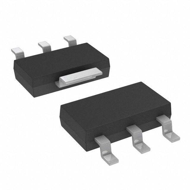
| 产品图片 |
|
| rohs | 符合RoHS无铅 / 符合限制有害物质指令(RoHS)规范要求 |
| 产品系列 | 电源管理 IC,低压差稳压器,Microchip Technology MCP1700T-3302E/MB- |
| 数据手册 | http://www.microchip.com/mymicrochip/filehandler.aspx?ddocname=en011779http://www.microchip.com/mymicrochip/filehandler.aspx?ddocname=en023833 |
| 产品型号 | MCP1700T-3302E/MB |
| PCN设计/规格 | http://www.microchip.com/mymicrochip/NotificationDetails.aspx?id=5619&print=view |
| 产品目录页面 | |
| 产品种类 | 低压差稳压器 |
| 供应商器件封装 | SOT-89-3 |
| 其它名称 | MCP1700T3302EMBDKR |
| 包装 | Digi-Reel® |
| 商标 | Microchip Technology |
| 回动电压—最大值 | 350 mV |
| 安装类型 | 表面贴装 |
| 安装风格 | SMD/SMT |
| 封装 | Reel |
| 封装/外壳 | TO-243AA |
| 封装/箱体 | SOT-89-3 |
| 工作温度 | -40°C ~ 125°C |
| 工厂包装数量 | 1000 |
| 最大功率耗散 | 1.635 W |
| 最大工作温度 | + 125 C |
| 最大输入电压 | 6 V |
| 最小工作温度 | - 40 C |
| 最小输入电压 | + 2.3 V |
| 标准包装 | 1 |
| 电压-跌落(典型值) | 0.178V @ 250mA |
| 电压-输入 | 最高 6V |
| 电压-输出 | 3.3V |
| 电压调节准确度 | 3 % |
| 电流-输出 | 250mA |
| 电流-限制(最小值) | - |
| 稳压器拓扑 | 正,固定式 |
| 稳压器数 | 1 |
| 线路调整率 | 0.75 % / V |
| 负载调节 | 1 % |
| 输入偏压电流—最大 | 0.0016 mA |
| 输出电压 | 3.3 V |
| 输出电流 | 250 mA |
| 输出端数量 | 1 Output |
| 输出类型 | Fixed |


- 商务部:美国ITC正式对集成电路等产品启动337调查
- 曝三星4nm工艺存在良率问题 高通将骁龙8 Gen1或转产台积电
- 太阳诱电将投资9.5亿元在常州建新厂生产MLCC 预计2023年完工
- 英特尔发布欧洲新工厂建设计划 深化IDM 2.0 战略
- 台积电先进制程称霸业界 有大客户加持明年业绩稳了
- 达到5530亿美元!SIA预计今年全球半导体销售额将创下新高
- 英特尔拟将自动驾驶子公司Mobileye上市 估值或超500亿美元
- 三星加码芯片和SET,合并消费电子和移动部门,撤换高东真等 CEO
- 三星电子宣布重大人事变动 还合并消费电子和移动部门
- 海关总署:前11个月进口集成电路产品价值2.52万亿元 增长14.8%


PDF Datasheet 数据手册内容提取
MCP1700 Low Quiescent Current LDO Features General Description • AEC-Q100 Qualified and PPAP Capable The MCP1700 is a family of CMOS low dropout (LDO) • 1.6µA Typical Quiescent Current voltage regulators that can deliver up to 250mA of current while consuming only 1.6µA of quiescent • Input Operating Voltage Range: 2.3V to 6.0V current (typical). The input operating range is specified • Output Voltage Range: 1.2V to 5.0V from 2.3V to 6.0V, making it an ideal choice for two and • 250mA Output Current for Output three primary cell battery-powered applications, as well Voltages2.5V as single cell Li-Ion-powered applications. • 200mA Output Current for Output The MCP1700 is capable of delivering 250mA with Voltages<2.5V only 178mV of input to output voltage differential • Low Dropout (LDO) Voltage (V =2.8V). The output voltage tolerance of the OUT - 178mV Typical @ 250mA for VOUT=2.8V MCP1700 is typically ±0.4% at +25°C and ±3% • 0.4% Typical Output Voltage Tolerance maximum over the operating junction temperature • Standard Output Voltage Options: range of -40°C to +125°C. - 1.2V, 1.8V, 2.5V, 2.8V, 2.9V, 3.0V, 3.3V, 5.0V Output voltages available for the MCP1700 range from • Stable with 1.0µF Ceramic Output Capacitor 1.2V to 5.0V. The LDO output is stable when using only 1µF output capacitance. Ceramic, tantalum or • Short Circuit Protection aluminum electrolytic capacitors can all be used for • Overtemperature Protection input and output. Overcurrent limit and overtemperature shutdown provide a robust solution for any application. Applications Package options include SOT-23, SOT-89, TO-92 and • Battery-Powered Devices 2x2 DFN-6. • Battery-Powered Alarm Circuits Package Types • Smoke Detectors • CO2 Detectors 3-Pin SOT-23 3-Pin SOT-89 • Pagers and Cellular Phones V V IN IN • Smart Battery Packs 3 • Low Quiescent Current Voltage Reference MCP1700 • PDAs MCP1700 • Digital Cameras 1 2 3 1 2 • Microcontroller Power GND VOUT GNDVINVOUT Related Literature 3-Pin TO-92 2x2 DFN-6* • AN765, “Using Microchip’s Micropower LDOs” VIN 1 6 VOUT (DS00765), Microchip Technology Inc., 2002 MCP1700 NC 2 EP 5 NC • AN766, “Pin-Compatible CMOS Upgrades to 1 2 3 7 BiPolar LDOs” (DS00766), GND 3 4 NC Microchip Technology Inc., 2002 • AN792, “A Method to Determine How Much Power a SOT23 Can Dissipate in an Application” GND V V IN OUT (DS00792), Microchip Technology Inc., 2001 * Includes Exposed Thermal Pad (EP); see Table3-1. 2005-2018 Microchip Technology Inc. DS20001826E-page 1
MCP1700 Functional Block Diagrams MCP1700 V V IN OUT Error Amplifier +V IN Voltage - Reference + Overcurrent Overtemperature GND Typical Application Circuits MCP1700 V GND IN (2.3V to 3.2V) VOUT VIN 1.8V VOUT CIN 1µF Ceramic I OUT C 150mA OUT 1µF Ceramic 2005-2018 Microchip Technology Inc. DS20001826E-page 2
MCP1700 1.0 ELECTRICAL † Notice: Stresses above those listed under “Maximum Ratings” may cause permanent damage to the device. This is CHARACTERISTICS a stress rating only, and functional operation of the device at those or any other conditions above those indicated in the Absolute Maximum Ratings † operational listings of this specification is not implied. Exposure to maximum rating conditions for extended periods VDD............................................................................................+6.5V may affect device reliability. All inputs and outputs w.r.t. .........(V -0.3V) to (V +0.3V) SS IN Peak Output Current....................................Internally Limited Storage Temperature....................................-65°C to +150°C Maximum Junction Temperature...................................150°C Operating Junction Temperature...................-40°C to +125°C ESD protection on all pins (HBM;MM)4kV; 400V DC CHARACTERISTICS Electrical Characteristics: Unless otherwise specified, all limits are established for V =V +1V, I =100µA, IN R LOAD C =1µF (X7R), C =1µF(X7R), T =+25°C. OUT IN A Boldface type applies for junction temperatures, T (Note6) of -40°C to +125°C. J Parameters Sym. Min. Typ. Max. Units Conditions Input/Output Characteristics Input Operating V 2.3 — 6.0 V Note1 IN Voltage Input Quiescent I — 1.6 4 µA I =0mA, V =V +1V q L IN R Current Maximum Output I 250 — — mA For V 2.5V OUT_mA R Current 200 — — For V 2.5V R Output Short I — 408 — mA V =V +1V, V =GND OUT_SC IN R OUT Circuit Current Current (peak current) measured 10ms after short is applied. Output Voltage V V -2.0% V ±0.4% V +2.0% V Note2 OUT R R R Regulation V -3.0% V +3.0% R R V Temperature TCV — 50 — ppm/°C Note3 OUT OUT Coefficient Line Regulation V / -1.0 ±0.75 +1.0 %/V (V +1)V V 6V OUT R IN (V XV ) OUT IN Load Regulation V /V -1.5 ±1.0 +1.5 % I =0.1mA to 250mA for V 2.5V OUT OUT L R I =0.1mA to 200mA for V 2.5V L R Note4 Dropout Voltage V -V — 178 350 mV I =250mA, (Note1, Note5) IN OUT L V 2.5V R Dropout Voltage V -V — 150 350 mV I =200mA, (Note1, Note5) IN OUT L V 2.5V R Output Rise Time T — 500 — µs 10%V to 90% V V =0V to 6V, R R R IN R =50 resistive L Note 1: The minimum V must meet two conditions: V 2.3V and V V +3.0%V . IN IN IN R DROPOUT 2: V is the nominal regulator output voltage. For example: V =1.2V, 1.5V, 1.8V, 2.5V, 2.8V, 2.9V, 3.0V, 3.3V, 4.0V, 5.0V. R R The input voltage V =V +1.0V; I =100µA. IN R OUT 3: TCV =(V -V ) *106 / (V *Temperature), V =highest voltage measured over the OUT OUT-HIGH OUT-LOW R OUT-HIGH temperature range. V =lowest voltage measured over the temperature range. OUT-LOW 4: Load regulation is measured at a constant junction temperature using low duty cycle pulse testing. Changes in output voltage due to heating effects are determined using thermal regulation specification TCV . OUT 5: Dropout voltage is defined as the input to output differential at which the output voltage drops 2% below its measured value with a V +1V differential applied. R 6: The maximum allowable power dissipation is a function of ambient temperature, the maximum allowable junction temperature and the thermal resistance from junction to air (i.e. T , T , ). Exceeding the maximum allowable power A J JA dissipation will cause the device operating junction temperature to exceed the maximum 150°C rating. Sustained junction temperatures above 150°C can impact the device reliability. 7: The junction temperature is approximated by soaking the device under test at an ambient temperature equal to the desired Junction temperature. The test time is small enough such that the rise in the Junction temperature over the ambient temperature is not significant. 2005-2018 Microchip Technology Inc. DS20001826E-page 3
MCP1700 DC CHARACTERISTICS (CONTINUED) Electrical Characteristics: Unless otherwise specified, all limits are established for V =V +1V, I =100µA, IN R LOAD C =1µF (X7R), C =1µF(X7R), T =+25°C. OUT IN A Boldface type applies for junction temperatures, T (Note6) of -40°C to +125°C. J Parameters Sym. Min. Typ. Max. Units Conditions Output Noise e — 3 — µV/(Hz)1/2 I =100mA, f=1kHz, C =1µF N L OUT Power Supply PSRR — 44 — dB f=100Hz, C =1µF, I =50mA, OUT L Ripple Rejection V =100mVpk-pk, C =0µF, INAC IN Ratio V =1.2V R Thermal T — 140 — °C V =V +1V, I = 100µA SD IN R L Shutdown Protection Note 1: The minimum V must meet two conditions: V 2.3V and V V +3.0%V . IN IN IN R DROPOUT 2: V is the nominal regulator output voltage. For example: V =1.2V, 1.5V, 1.8V, 2.5V, 2.8V, 2.9V, 3.0V, 3.3V, 4.0V, 5.0V. R R The input voltage V =V +1.0V; I =100µA. IN R OUT 3: TCV =(V -V ) *106 / (V *Temperature), V =highest voltage measured over the OUT OUT-HIGH OUT-LOW R OUT-HIGH temperature range. V =lowest voltage measured over the temperature range. OUT-LOW 4: Load regulation is measured at a constant junction temperature using low duty cycle pulse testing. Changes in output voltage due to heating effects are determined using thermal regulation specification TCV . OUT 5: Dropout voltage is defined as the input to output differential at which the output voltage drops 2% below its measured value with a V +1V differential applied. R 6: The maximum allowable power dissipation is a function of ambient temperature, the maximum allowable junction temperature and the thermal resistance from junction to air (i.e. T , T , ). Exceeding the maximum allowable power A J JA dissipation will cause the device operating junction temperature to exceed the maximum 150°C rating. Sustained junction temperatures above 150°C can impact the device reliability. 7: The junction temperature is approximated by soaking the device under test at an ambient temperature equal to the desired Junction temperature. The test time is small enough such that the rise in the Junction temperature over the ambient temperature is not significant. TEMPERATURE SPECIFICATIONS Electrical Characteristics: Unless otherwise specified, all limits are established for V =V +1V, I =100µA, IN R LOAD C =1µF (X7R), C =1µF (X7R), T =+25°C. OUT IN A Boldface type applies for junction temperatures, T (Note1) of -40°C to +125°C. J Parameters Sym. Min. Typ. Max. Units Conditions Temperature Ranges Specified Temperature Range T -40 +125 °C A Operating Temperature Range T -40 +125 °C J Storage Temperature Range T -65 +150 °C A Thermal Package Resistance Thermal Resistance, 2x2 DFN — 91 — °C/W EIA/JEDEC® JESD51-7 JA — 286 — °C/W FR-4 4-Layer Board JC(Top) — 28.57 — °C/W JC(Bottom) — 8.95 — °C/W JT Thermal Resistance, SOT-23 — 212 — °C/W EIA/JEDEC JESD51-7 JA — 139 — °C/W FR-4 4-Layer Board JC(Top) — 11.95 — °C/W JC(Bottom) — 6.15 — °C/W JT Thermal Resistance, SOT-89 — 104 — °C/W EIA/JEDEC JESD51-7 JA — 74 — °C/W FR-4 4-Layer Board JC(Top) — 30 — °C/W JT Note 1: The maximum allowable power dissipation is a function of ambient temperature, the maximum allowable junction temperature and the thermal resistance from junction to air (i.e. T , T , ). Exceeding the maximum allowable power A J JA dissipation will cause the device operating junction temperature to exceed the maximum 150°C rating. Sustained junction temperatures above 150°C can impact the device reliability. 2005-2018 Microchip Technology Inc. DS20001826E-page 4
MCP1700 TEMPERATURE SPECIFICATIONS (CONTINUED) Electrical Characteristics: Unless otherwise specified, all limits are established for V =V +1V, I =100µA, IN R LOAD C =1µF (X7R), C =1µF (X7R), T =+25°C. OUT IN A Boldface type applies for junction temperatures, T (Note1) of -40°C to +125°C. J Parameters Sym. Min. Typ. Max. Units Conditions Thermal Resistance, TO-92 — 92 — °C/W EIA/JEDEC JESD51-7 JA — 74 — °C/W FR-4 4-Layer Board JC(Top) Note 1: The maximum allowable power dissipation is a function of ambient temperature, the maximum allowable junction temperature and the thermal resistance from junction to air (i.e. T , T , ). Exceeding the maximum allowable power A J JA dissipation will cause the device operating junction temperature to exceed the maximum 150°C rating. Sustained junction temperatures above 150°C can impact the device reliability. 2005-2018 Microchip Technology Inc. DS20001826E-page 5
MCP1700 2.0 TYPICAL PERFORMANCE CURVES Note: The graphs and tables provided following this note are a statistical summary based on a limited number of samples and are provided for informational purposes only. The performance characteristics listed herein are not tested or guaranteed. In some graphs or tables, the data presented may be outside the specified operating range (e.g., outside specified power supply range) and therefore outside the warranted range. Note: Unless otherwise indicated: V =1.8V, C =1µF Ceramic (X7R), C =1µF Ceramic (X7R), I =100µA, R OUT IN L T =+25°C, V =V +1V. A IN R Note: Junction Temperature (T) is approximated by soaking the device under test to an ambient temperature equal to the desired junction J temperature. The test time is small enough such that the rise in Junction temperature over the Ambient temperature is not significant. 3.0 1.208 µA) 22..68 VIORUT== 1 0.2 µVA TJ= +125°C V)11..220046 TJ= +125°C VIORUT== 1 0.2.1V mA nt Current ( 222...024 TJ= -40°C ut Voltage (111...122900802 TJ= +25°C scees 11..86 TJ= +25°C utpOu11..119966 ui 1.194 Q 1.4 TJ= -40°C 1.192 1.2 1.0 1.190 2.0 2.5 3.0 3.5 4.0 4.5 5.0 5.5 6.0 2.0 2.5 3.0 3.5 4.0 4.5 5.0 5.5 6.0 Input Voltage (V) Input Voltage (V) FIGURE 2-1: Input Quiescent Current vs. FIGURE 2-4: Output Voltage vs. Input Input Voltage. Voltage (V =1.2V). R 50 1.800 A) 4405 VR= 2.8V TJ= +125°C 1.795 VIORUT== 1 0.8.1V mA nt (µ 35 TJ= +25°C e (V)1.790 e 30 g nd Curr 2205 TJ= -40°C ut Volta1.785 TJ= -40°C TJ= +125°C uGrou 1105 pOutp111..777788500 TJ= +25°C 5 0 1.770 0 25 50 75 100 125 150 175 200 225 250 2.0 2.5 3.0 3.5 4.0 4.5 5.0 5.5 6.0 Load Current (mA) Input Voltage (V) FIGURE 2-2: Ground Current vs. Load FIGURE 2-5: Output Voltage vs. Input Current. Voltage (V =1.8V). R 2.50 2.800 VIN= VR+ 1V 2.798 VR= 2.8V cent Current (µA)Quiesc1221....70255050 VRV=R 5=. 01V.2V VR= 2.8IVOUT= 0 µA utput Voltage (V)Ou 22222222........777777778899998868024624 TJ= +1T2J5=°C -40°CTJ= +25°C IOUT= 0.1 mA 2.780 1.25 2.778 -40 -25 -10 5 20 35 50 65 80 95 110125 3.3 3.6 3.9 4.2 4.5 4.8 5.1 5.4 5.7 6.0 Junction Temperature (°C) Input Voltage (V) FIGURE 2-3: Quiescent Current vs. FIGURE 2-6: Output Voltage vs. Input Junction Temperature. Voltage (V =2.8V). R 2005-2018 Microchip Technology Inc. DS20001826E-page 6
MCP1700 Note: Unless otherwise indicated: V =1.8V, C =1µF Ceramic (X7R), C =1µF Ceramic (X7R), I =100µA, R OUT IN L T =+25°C, V =V +1V. A IN R 5.000 2.798 TJ= +25°C 4.995 VIORUT== 5 0.0.1V mA TJ= +25°C 2.796 ge (V)44..998950 TJ= -40°C ge (V)22..779924 VVRIN== 2V.8RV+ 1V Volta4.980 Volta22..778980 TJ= -40°C ut 4.975 ut 2.786 tpOu444...999767050 TJ= +125°C utpOu222..777888244 TJ= +125°C 4.960 2.780 4.955 2.778 5.0 5.2 5.4 5.6 5.8 6.0 0 50 100 150 200 250 Input Voltage (V) Load Current (mA) FIGURE 2-7: Output Voltage vs. Input FIGURE 2-10: Output Voltage vs. Load Voltage (V =5.0V). Current (V =2.8V). R R 1.21 5.000 1.20 TJ= -40°C VVRIN== 1V.2RV+ 1V 4.995 TJ= +25°C V) V) 4.990 age (1.19 TJ= +25°C age ( 4.985 TJ= -40°C Volt1.18 Volt 4.980 VR= 5.0V ut ut 4.975 VIN= VR+ 1V tpu11..1177 TTJJ=++112255°CC tpu 44.997700 O O 1.16 4.965 TJ= +125°C 4.960 1.15 4.955 0 25 50 75 100 125 150 175 200 0 50 100 150 200 250 Load Current (mA) Load Current (mA) FIGURE 2-8: Output Voltage vs. Load FIGURE 2-11: Output Voltage vs. Load Current (V =1.2V). Current (V =5.0V). R R 1.792 0.25 VR= 2.8V 1.790 utput Voltage (V)Ou1111....777788884682 TJ= +25°C TJ= +125°C TJ= -40°C pout Votage (V)op000...112050 TJ= +25°C TJ=TT J+==1 2-544°00C°°CC VR= 1.8V Dr0.05 1.780 VIN= VR+ 1V 1.778 0.00 0 25 50 75 100 125 150 175 200 0 25 50 75 100 125 150 175 200 225 250 Load Current (mA) Load Current (mA) FIGURE 2-9: Output Voltage vs. Load FIGURE 2-12: Dropout Voltage vs. Load Current (V =1.8V). Current (V =2.8V). R R 2005-2018 Microchip Technology Inc. DS20001826E-page 7
MCP1700 Note: Unless otherwise indicated: V =1.8V, C =1µF Ceramic (X7R), C =1µF Ceramic (X7R), I =100µA, R OUT IN L T =+25°C, V =V +1V. A IN R 0.16 10.00 0.14 VR= 5.0V VVIRN== 23..88VV V)0.12 TJ= +125°C z) IOUT= 50 mA Voltage (00..0180 TJ= +25°C √e (µV/H 1.00 IVVOIRUNT=== 12 5..250VV mA VIVOIRUNT=== 12 5..880VV mA ut 0.06 ois oo NN 00.1100 op0.04 TJ= -40°C Dr 0.02 0.00 0.01 0 25 50 75 100 125 150 175 200 225 250 0.01 0.1 1 10 100 1000 Load Current (mA) Frequency (kHz) FIGURE 2-13: Dropout Voltage vs. Load FIGURE 2-16: Noise vs. Frequency. Current (V =5.0V). R +20 VIN=2.2V +10 CIN=1µF Ceramic 0 COUT=1µF Ceramic de) -10 a dec -20 VR=1.2V dB/ -30 RR ( -40 S P -50 I=100mA -60 Load -70 Step 0.01 0.10 1.00 10.0 100 1000 Frequency ((cid:75)Hz) FIGURE 2-14: Power Supply Ripple FIGURE 2-17: Dynamic Load Step Rejection vs. Frequency (V =1.2V). (V =1.2V). R R +20 VIN=2.8V +10 0 CIN=1µF Ceramic de) -10 COUT=1µF Ceramic a Dec -20 VR=1.8V dB/ -30 RR ( -40 I=100mA PS -50 Load -60 Step 0.01 0.01 1(cid:14)(cid:16) (cid:16) 10.00 100 1000 Frequency ((cid:75)Hz) FIGURE 2-15: Power Supply Ripple FIGURE 2-18: Dynamic Load Step Rejection vs. Frequency (V =2.8V). (V =1.8V). R R 2005-2018 Microchip Technology Inc. DS20001826E-page 8
MCP1700 Note: Unless otherwise indicated: V =1.8V, C =1µF Ceramic (X7R), C = µF Ceramic (X7R), I =100µA, R OUT IN L T =+25°C, V =V +1V. A IN R VIN=6V VIN=3.8V CCIONU=T1=µ2F2 CµFe r(a1mi cESR) VR=5V CIN=1µF Ceramic COUT=1µF Ceramic VR=2.8V IL=oa1d00mA ILOoUaTd= S2t0e0pmA Step FIGURE 2-19: Dynamic Load Step FIGURE 2-22: Dynamic Load Step (V =2.8V). (V =5.0V). R R VIN=2.8V VIN=3.8V to CIN=1µF Ceramic 4.8V COUT=1µF Ceramic COUT=22µF (1 ESR) VR=1.8V VR=2.8V ILOoUaTd= S2t0e0pmA IOUT 100mA FIGURE 2-20: Dynamic Load Step FIGURE 2-23: Dynamic Line Step (V =1.8V). (V =2.8V). R R VIN=3.8V VIN=0V to CCIONU=T1=µ2F2 µCFe r(a1mi cESR) 2.2V RCLOOUATD==12µ5F Ceramic VR=2.8V IOUT=200mA VR=1.2V Load Step FIGURE 2-21: Dynamic Load Step FIGURE 2-24: Start-up from V IN (V =2.8V). (V =1.2V). R R 2005-2018 Microchip Technology Inc. DS20001826E-page 9
MCP1700 Note: Unless otherwise indicated: V =1.8V, C =1µF Ceramic (X7R), C =1µF Ceramic (X7R), I =100µA, R OUT IN L T =+25°C, V =V +1V. A IN R VIN=0V to 2.8V COUT=1µF Ceramic 0.0 RLOAD=25 %)-0.1 VIN= 5.0V VIN= 4.3V VIORUT== 2 0.8 tVo 250 mA n (-0.2 o ati-0.3 ul g Re-0.4 ad oa-0.5 VIINN= 3.3V VR=1.8V L -0.6 -0.7 -40 -25 -10 5 20 35 50 65 80 95 110 125 Junction Temperature (°C) FIGURE 2-25: Start-up from V FIGURE 2-28: Load Regulation vs. IN (V =1.8V). Junction Temperature (V =2.8V). R R V3.I8NV=0V to COUT=1µF Ceramic 0.10 RLOAD=25 VR= 5.0V %) 0.05 IOUT= 0 to 250 mA n ( VIN= 6.0V o 0.00 ati ul g-0.05 e R d ad-00.1100 VIINN=55.55V o VR=2.8V L -0.15 -0.20 -40 -25 -10 5 20 35 50 65 80 95 110 125 Junction Temperature (°C) FIGURE 2-26: Start-up from V FIGURE 2-29: Load Regulation vs. IN (V =2.8V). Junction Temperature (V =5.0V). R R 0.3 0.10 %) 0.2 VIN= 5.0V VIORUT== 1 0.8 tVo 200 mA V) 0.05 ulation ( 00..01 VIN= 3.5V ation (%/-00..0005 VR= 2.8V Reg -0.1 egul-0.10 VR= 1.8V d R-0.15 aLoa --000..223 VIN= 2.2V Line--00..2250 VR= 1.2V -0.4 -0.30 -40 -25 -10 5 20 35 50 65 80 95 110 125 -40 -25 -10 5 20 35 50 65 80 95 110125 Junction Temperature (°C) Junction Temperature (°C) FIGURE 2-27: Load Regulation vs. FIGURE 2-30: Line Regulation vs. Junction Temperature (V =1.8V). Temperature (V =1.2V, 1.8V, 2.8V). R R 2005-2018 Microchip Technology Inc. DS20001826E-page 10
MCP1700 3.0 PIN DESCRIPTIONS The descriptions of the pins are listed in Table3-1. TABLE 3-1: PIN FUNCTION TABLE Pin No. Pin No. Pin No. Pin No. Name Function SOT-23 SOT-89 TO-92 2x2 DFN-6 1 1 1 3 GND Ground Terminal 2 3 3 6 V Regulated Voltage Output OUT 3 2 2 1 V Unregulated Supply Voltage IN — — — 2, 4, 5 NC No Connect — — — 7 EP Exposed Thermal Pad 3.1 Ground Terminal (GND) 3.4 No Connect (NC) Regulator ground. Tie GND to the negative side of the No internal connection. The pins marked NC are true output and the negative side of the input capacitor. “No Connect” pins. Only the LDO bias current (1.6µA typical) flows out of this pin; there is no high current. The LDO output 3.5 Exposed Thermal Pad (EP) regulation is referenced to this pin. Minimize voltage drops between this pin and the negative side of the There is an internal electrical connection between the load. Exposed Thermal Pad (EP) and the GND pin; they must be connected to the same potential on the Printed 3.2 Regulated Output Voltage (V ) Circuit Board (PCB). OUT Connect V to the positive side of the load and the OUT positive terminal of the output capacitor. The positive side of the output capacitor should be physically located as close to the LDO V pin as is practical. OUT The current flowing out of this pin is equal to the DC load current. 3.3 Unregulated Input Voltage Pin (V ) IN Connect V to the input unregulated source voltage. IN As with all low dropout linear regulators, low source impedance is necessary for the stable operation of the LDO. The amount of capacitance required to ensure low source impedance will depend on the proximity of the input source capacitors or battery type. For most applications, 1µF of capacitance will ensure stable operation of the LDO circuit. For applications that have load currents below 100mA, the input capacitance requirement can be lowered. The type of capacitor used can be ceramic, tantalum or aluminum electrolytic. The low ESR characteristics of the ceramic will yield better noise and PSRR performance at high frequency. 2005-2018 Microchip Technology Inc. DS20001826E-page 11
MCP1700 4.0 DETAILED DESCRIPTION 4.1 Output Regulation 4.3 Overtemperature A portion of the LDO output voltage is fed back to the The internal power dissipation within the LDO is a internal error amplifier and compared with the precision function of input-to-output voltage differential and load internal bandgap reference. The error amplifier output current. If the power dissipation within the LDO is will adjust the amount of current that flows through the excessive, the internal junction temperature will rise P-Channel pass transistor, thus regulating the output above the typical shutdown threshold of 140°C. At that voltage to the desired value. Any changes in input point, the LDO will shut down and begin to cool to the voltage or output current will cause the error amplifier typical turn-on junction temperature of 130°C. If the to respond and adjust the output voltage to the target power dissipation is low enough, the device will voltage (refer to Figure4-1). continue to cool and operate normally. If the power dissipation remains high, the thermal shutdown 4.2 Overcurrent protection circuitry will again turn off the LDO, protecting it from catastrophic failure. The MCP1700 internal circuitry monitors the amount of current flowing through the P-Channel pass transistor. In the event of a short circuit or excessive output current, the MCP1700 will turn off the P-Channel device for a short period, after which the LDO will attempt to restart. If the excessive current remains, the cycle will repeat itself. MCP1700 V V IN OUT Error Amplifier +V IN Voltage - Reference + Overcurrent Overtemperature GND FIGURE 4-1: Block Diagram. 2005-2018 Microchip Technology Inc. DS20001826E-page 12
MCP1700 5.0 FUNCTIONAL DESCRIPTION The MCP1700 CMOS low dropout linear regulator is intended for applications that need the lowest current consumption while maintaining output voltage regulation. The operating continuous load of the MCP1700 ranges from 0mA to 250mA (V 2.5V). R The input operating voltage ranges from 2.3V to 6.0V, making it capable of operating from two, three or four alkaline cells or a single Li-Ion cell battery input. 5.1 Input The input of the MCP1700 is connected to the source of the P-Channel PMOS pass transistor. As with all LDO circuits, a relatively low source impedance (10) is needed to prevent the input impedance from causing the LDO to become unstable. The size and type of the required capacitor depend heavily on the input source type (battery, power supply) and the output current range of the application. For most applications (up to 100mA), a 1µF ceramic capacitor will be sufficient to ensure circuit stability. Larger values can be used to improve circuit AC performance. 5.2 Output The maximum rated continuous output current for the MCP1700 is 250mA (V 2.5V). For applications R where V <2.5V, the maximum output current is R 200mA. A minimum output capacitance of 1.0µF is required for small signal stability in applications that have up to 250mA output current capability. The capacitor type can be ceramic, tantalum or aluminum electrolytic. The ESR range on the output capacitor can range from 0 to 2.0. 5.3 Output Rise time When powering up the internal reference output, the typical output rise time of 500µs is controlled to prevent overshoot of the output voltage. 2005-2018 Microchip Technology Inc. DS20001826E-page 13
MCP1700 6.0 APPLICATION CIRCUITS AND The maximum continuous operating junction ISSUES temperature specified for the MCP1700 is +125°C. To estimate the internal junction temperature of the MCP1700, the total internal power dissipation is 6.1 Typical Application multiplied by the thermal resistance from junction to ambient (R ). The thermal resistance from junction to The MCP1700 is most commonly used as a voltage JA ambient for the SOT-23 pin package is estimated at regulator. Its low quiescent current and low dropout 230°C/W. voltage make it ideal for many battery-powered applications. EQUATION 6-2: MCP1700 T = P R +T JMAX TOTAL JA AMAX V IN V GND (2.3V to 3.2V) 1.O8UVT VOUT VIN CIN TJ(MAX) = Mtemaxpimeruamtu rceontinuous junction IOUT C 1µF Ceramic PTOTAL = Total power dissipation of the device 150mA OUT 1µF Ceramic RJA = Thermal resistance from junction to ambient FIGURE 6-1: Typical Application Circuit. TA(MAX) = Maximum ambient temperature 6.1.1 APPLICATION INPUT CONDITIONS The maximum power dissipation capability for a package can be calculated given the junction-to- Package Type = SOT-23 ambient thermal resistance and the maximum ambient Input Voltage Range = 2.3V to 3.2V temperature for the application. The following equation V maximum = 3.2V can be used to determine the maximum internal power IN dissipation of the package. V typical = 1.8V OUT I = 150mA maximum OUT EQUATION 6-3: 6.2 Power Calculations T –T P = ------J-----M----A---X---------------A-----M----A---X------ DMAX R JA 6.2.1 POWER DISSIPATION P = Maximum power dissipation of the The internal power dissipation of the MCP1700 is a D(MAX) device function of input voltage, output voltage and output current. The power dissipation resulting from the TJ(MAX) = Maximum continuous junction quiescent current draw is so low it is insignificant temperature (1.6µA x VIN). The following equation can be used to TA(MAX) = Maximum ambient temperature calculate the internal power dissipation of the LDO. R = Thermal resistance from junction to JA ambient EQUATION 6-1: PLDO = VINMAX–VOUTMINIOUTMAX EQUATION 6-4: T = P R P = Internal power dissipation of the JRISE DMAX JA LDO LDO Pass device T = Rise in the device’s junction V = Maximum input voltage J(RISE) IN(MAX) temperature over the ambient V = Minimum output voltage of the OUT(MIN) temperature LDO P = Maximum power dissipation of the TOTAL device R = Thermal resistance from junction to JA ambient 2005-2018 Microchip Technology Inc. DS20001826E-page 14
MCP1700 EQUATION 6-5: T = P xR J(RISE) TOTAL JA T = T +T J JRISE A TJ(RISE) = 218.1milliwattsx212.0°C/Watt T = Junction Temperature TJ(RISE) = 46.2°C J T = Rise in the device’s junction Junction Temperature Estimate J(RISE) temperature over the ambient To estimate the internal junction temperature, the temperature calculated temperature rise is added to the ambient or T = Ambient temperature offset temperature. For this example, the worst-case A junction temperature is estimated below. 6.3 Voltage Regulator T = T +T J J(RISE) A(MAX) Internal power dissipation, junction temperature rise, T = 86.2°C J junction temperature and maximum power dissipation Maximum Package Power Dissipation at +40°C are calculated in the following example. The power Ambient Temperature dissipation resulting from ground current is small 2x2 DFN-6 (91°C/Watt= ) enough to be neglected. JA P = (125°C-40°C)/91°C/W D(MAX) 6.3.1 POWER DISSIPATION EXAMPLE P = 934milliwatts D(MAX) Package SOT-23 (212.0°C/Watt= ) JA Package Type = SOT-23 P = (125°C-40°C)/212°C/W D(MAX) Input Voltage P = 401milliwatts D(MAX) V = 2.3V to 3.2V SOT-89 (104°C/Watt= ) IN JA LDO Output Voltages and Currents P = (125°C-40°C)/104°C/W D(MAX) V = 1.8V P = 817milliwatts OUT D(MAX) I = 150mA TO-92 (92°C/Watt= ) OUT JA Maximum Ambient Temperature P = (125°C-40°C)/92°C/W D(MAX) T = +40°C P = 924milliwatts A(MAX) D(MAX) Internal Power Dissipation Internal Power dissipation is the product of the LDO output current times the voltage across the LDO (V to V ). IN OUT P = (V -V )xI LDO(MAX) IN(MAX) OUT(MIN) OUT(MAX) P = (3.2V-(0.97x1.8V))x150mA LDO P = 218.1milliwatts LDO Device Junction Temperature Rise The internal junction temperature rise is a function of internal power dissipation and the thermal resistance from junction to ambient for the application. The thermal resistance from junction to ambient (R ) is derived JA from an EIA/JEDEC® standard for measuring thermal resistance for small surface mount packages. The EIA/ JEDEC specification is JESD51-7, “High Effective Thermal Conductivity Test Board for Leaded Surface Mount Packages”. The standard describes the test method and board specifications for measuring the thermal resistance from junction to ambient. The actual thermal resistance for a particular application can vary depending on many factors, such as copper area and thickness. Refer to AN792, “A Method to Determine How Much Power a SOT-23 Can Dissipate in an Application” (DS00792), for more information regarding this subject. 2005-2018 Microchip Technology Inc. DS20001826E-page 15
MCP1700 6.4 Voltage Reference The MCP1700 can be used not only as a regulator, but also as a low quiescent current voltage reference. In many microcontroller applications, the initial accuracy of the reference can be calibrated using production test equipment or by using a ratio measurement. When the initial accuracy is calibrated, the thermal stability and line regulation tolerance are the only errors introduced by the MCP1700 LDO. The low cost, low quiescent current and small ceramic output capacitor are all advantages when using the MCP1700 as a voltage reference. Ratio Metric Reference 1 µA Bias PIC® MCP1700 Microcontroller V C1IµNF GINNVDOUT COUT VREF 1µF AD0 AD1 Bridge Sensor FIGURE 6-2: Using the MCP1700 as a voltage reference. 6.5 Pulsed Load Applications For some applications, there are pulsed load current events that may exceed the specified 250mA maximum specification of the MCP1700. The internal current limit of the MCP1700 will prevent high peak load demands from causing non-recoverable damage. The 250mA rating is a maximum average continuous rating. As long as the average current does not exceed 250mA, pulsed higher load currents can be applied to the MCP1700. The typical current limit for the MCP1700 is 550mA (T +25°C). A 2005-2018 Microchip Technology Inc. DS20001826E-page 16
MCP1700 7.0 PACKAGING INFORMATION 7.1 Package Marking Information 3-Pin SOT-23 Standard Extended Temp Symbol Voltage * CKNN CK 1.2 CM 1.8 CP 2.5 CQ 2.8 3-Pin SOT-89 GC 2.9 CR 3.0 CS 3.3 CUYYWW CU 5.0 NNN * Custom output voltages available upon request. Contact your local Microchip sales office for more information. 3-Pin TO-92 Example XXXXXX 1700 XXXXXX 1202E XXXXXX TO^e^3 YWWNNN 322256 6-Lead DFN (2x2x0.9 mm) Example Part Number Code ABB MCP1700T-1202E/MAY ABB 256 MCP1700T-1802E/MAY ABC MCP1700T-2502E/MAY ABD MCP1700T-2802E/MAY ABF MCP1700T-3002E/MAY ABE MCP1700T-3302E/MAY AAZ MCP1700T-5002E/MAY ABA Legend: XX...X Customer-specific information Y Year code (last digit of calendar year) YY Year code (last 2 digits of calendar year) WW Week code (week of January 1 is week ‘01’) NNN Alphanumeric traceability code e3 Pb-free JEDEC® designator for Matte Tin (Sn) * This package is Pb-free. The Pb-free JEDEC designator ( e 3 ) can be found on the outer packaging for this package. Note: In the event the full Microchip part number cannot be marked on one line, it will be carried over to the next line, thus limiting the number of available characters for customer-specific information. 2005-2018 Microchip Technology Inc. DS20001826E-page 17
MCP1700 (cid:2)(cid:3)(cid:4)(cid:5)(cid:6)(cid:7)(cid:8)(cid:9)(cid:10)(cid:6)(cid:11)(cid:12)(cid:13)(cid:14)(cid:8)(cid:15)(cid:16)(cid:6)(cid:10)(cid:10)(cid:8)(cid:17)(cid:18)(cid:12)(cid:10)(cid:13)(cid:19)(cid:5)(cid:8)(cid:20)(cid:21)(cid:6)(cid:19)(cid:11)(cid:13)(cid:11)(cid:12)(cid:22)(cid:21)(cid:8)(cid:23)(cid:20)(cid:20)(cid:24)(cid:8)(cid:25)(cid:15)(cid:17)(cid:20)(cid:3)(cid:26)(cid:2)(cid:27) (cid:28)(cid:22)(cid:12)(cid:5)(cid:29) .(cid:22)(cid:21)(cid:14)#(cid:23)(cid:13)(cid:14)(cid:31)(cid:22) #(cid:14)(cid:20)$(cid:21)(cid:21)(cid:13)(cid:25)#(cid:14)(cid:10)(cid:11)(cid:20)/(cid:11)(cid:12)(cid:13)(cid:14)!(cid:21)(cid:11)-(cid:19)(cid:25)(cid:12) 1(cid:14)(cid:10)(cid:26)(cid:13)(cid:11) (cid:13)(cid:14) (cid:13)(cid:13)(cid:14)#(cid:23)(cid:13)(cid:14)(cid:18)(cid:19)(cid:20)(cid:21)(cid:22)(cid:20)(cid:23)(cid:19)(cid:10)(cid:14)2(cid:11)(cid:20)/(cid:11)(cid:12)(cid:19)(cid:25)(cid:12)(cid:14)(cid:3)(cid:10)(cid:13)(cid:20)(cid:19)%(cid:19)(cid:20)(cid:11)#(cid:19)(cid:22)(cid:25)(cid:14)(cid:26)(cid:22)(cid:20)(cid:11)#(cid:13)!(cid:14)(cid:11)#(cid:14) (cid:23)##(cid:10)+33---(cid:29)(cid:31)(cid:19)(cid:20)(cid:21)(cid:22)(cid:20)(cid:23)(cid:19)(cid:10)(cid:29)(cid:20)(cid:22)(cid:31)3(cid:10)(cid:11)(cid:20)/(cid:11)(cid:12)(cid:19)(cid:25)(cid:12) b N E E1 1 2 e e1 D c A A2 φ A1 L 4(cid:25)(cid:19)# (cid:18)(cid:28)55(cid:28)(cid:18)"(cid:24)"(cid:8)(cid:3) (cid:2)(cid:19)(cid:31)(cid:13)(cid:25) (cid:19)(cid:22)(cid:25)(cid:14)5(cid:19)(cid:31)(cid:19)# (cid:18)(cid:28)6 67(cid:18) (cid:18)(cid:7)8 6$(cid:31)9(cid:13)(cid:21)(cid:14)(cid:22)%(cid:14)2(cid:19)(cid:25) 6 : 5(cid:13)(cid:11)!(cid:14)2(cid:19)#(cid:20)(cid:23) (cid:13) (cid:4)(cid:29)(cid:6)’(cid:14))(cid:3)* 7$# (cid:19)!(cid:13)(cid:14)5(cid:13)(cid:11)!(cid:14)2(cid:19)#(cid:20)(cid:23) (cid:13)(cid:30) (cid:30)(cid:29)(cid:6)(cid:4)(cid:14))(cid:3)* 7,(cid:13)(cid:21)(cid:11)(cid:26)(cid:26)(cid:14);(cid:13)(cid:19)(cid:12)(cid:23)# (cid:7) (cid:4)(cid:29)(cid:16)(cid:6) < (cid:30)(cid:29)(cid:30)(cid:15) (cid:18)(cid:22)(cid:26)!(cid:13)!(cid:14)2(cid:11)(cid:20)/(cid:11)(cid:12)(cid:13)(cid:14)(cid:24)(cid:23)(cid:19)(cid:20)/(cid:25)(cid:13) (cid:7)(cid:15) (cid:4)(cid:29)(cid:17)(cid:6) (cid:4)(cid:29)(cid:6)’ (cid:30)(cid:29)(cid:4)(cid:15) (cid:3)#(cid:11)(cid:25)!(cid:22)%% (cid:7)(cid:30) (cid:4)(cid:29)(cid:4)(cid:30) < (cid:4)(cid:29)(cid:30)(cid:4) 7,(cid:13)(cid:21)(cid:11)(cid:26)(cid:26)(cid:14)=(cid:19)!#(cid:23) " (cid:15)(cid:29)(cid:30)(cid:4) < (cid:15)(cid:29)>(cid:5) (cid:18)(cid:22)(cid:26)!(cid:13)!(cid:14)2(cid:11)(cid:20)/(cid:11)(cid:12)(cid:13)(cid:14)=(cid:19)!#(cid:23) "(cid:30) (cid:30)(cid:29)(cid:30)> (cid:30)(cid:29):(cid:4) (cid:30)(cid:29)(cid:5)(cid:4) 7,(cid:13)(cid:21)(cid:11)(cid:26)(cid:26)(cid:14)5(cid:13)(cid:25)(cid:12)#(cid:23) (cid:2) (cid:15)(cid:29)>(cid:17) (cid:15)(cid:29)(cid:6)(cid:4) :(cid:29)(cid:4)’ .(cid:22)(cid:22)#(cid:14)5(cid:13)(cid:25)(cid:12)#(cid:23) 5 (cid:4)(cid:29)(cid:30): (cid:4)(cid:29)’(cid:4) (cid:4)(cid:29)>(cid:4) .(cid:22)(cid:22)#(cid:14)(cid:7)(cid:25)(cid:12)(cid:26)(cid:13) (cid:3) (cid:4)? < (cid:30)(cid:4)? 5(cid:13)(cid:11)!(cid:14)(cid:24)(cid:23)(cid:19)(cid:20)/(cid:25)(cid:13) (cid:20) (cid:4)(cid:29)(cid:4)(cid:16) < (cid:4)(cid:29)(cid:15)(cid:4) 5(cid:13)(cid:11)!(cid:14)=(cid:19)!#(cid:23) 9 (cid:4)(cid:29):(cid:4) < (cid:4)(cid:29)’(cid:5) (cid:28)(cid:22)(cid:12)(cid:5)(cid:11)(cid:29) (cid:30)(cid:29) (cid:2)(cid:19)(cid:31)(cid:13)(cid:25) (cid:19)(cid:22)(cid:25) (cid:14)(cid:2)(cid:14)(cid:11)(cid:25)!(cid:14)"(cid:30)(cid:14)!(cid:22)(cid:14)(cid:25)(cid:22)#(cid:14)(cid:19)(cid:25)(cid:20)(cid:26)$!(cid:13)(cid:14)(cid:31)(cid:22)(cid:26)!(cid:14)%(cid:26)(cid:11) (cid:23)(cid:14)(cid:22)(cid:21)(cid:14)(cid:10)(cid:21)(cid:22)#(cid:21)$ (cid:19)(cid:22)(cid:25) (cid:29)(cid:14)(cid:18)(cid:22)(cid:26)!(cid:14)%(cid:26)(cid:11) (cid:23)(cid:14)(cid:22)(cid:21)(cid:14)(cid:10)(cid:21)(cid:22)#(cid:21)$ (cid:19)(cid:22)(cid:25) (cid:14) (cid:23)(cid:11)(cid:26)(cid:26)(cid:14)(cid:25)(cid:22)#(cid:14)(cid:13)&(cid:20)(cid:13)(cid:13)!(cid:14)(cid:4)(cid:29)(cid:15)’(cid:14)(cid:31)(cid:31)(cid:14)(cid:10)(cid:13)(cid:21)(cid:14) (cid:19)!(cid:13)(cid:29) (cid:15)(cid:29) (cid:2)(cid:19)(cid:31)(cid:13)(cid:25) (cid:19)(cid:22)(cid:25)(cid:19)(cid:25)(cid:12)(cid:14)(cid:11)(cid:25)!(cid:14)#(cid:22)(cid:26)(cid:13)(cid:21)(cid:11)(cid:25)(cid:20)(cid:19)(cid:25)(cid:12)(cid:14)(cid:10)(cid:13)(cid:21)(cid:14)(cid:7)(cid:3)(cid:18)"(cid:14)((cid:30)(cid:5)(cid:29)’(cid:18)(cid:29) )(cid:3)*+ )(cid:11) (cid:19)(cid:20)(cid:14)(cid:2)(cid:19)(cid:31)(cid:13)(cid:25) (cid:19)(cid:22)(cid:25)(cid:29)(cid:14)(cid:24)(cid:23)(cid:13)(cid:22)(cid:21)(cid:13)#(cid:19)(cid:20)(cid:11)(cid:26)(cid:26)(cid:27)(cid:14)(cid:13)&(cid:11)(cid:20)#(cid:14),(cid:11)(cid:26)$(cid:13)(cid:14) (cid:23)(cid:22)-(cid:25)(cid:14)-(cid:19)#(cid:23)(cid:22)$#(cid:14)#(cid:22)(cid:26)(cid:13)(cid:21)(cid:11)(cid:25)(cid:20)(cid:13) (cid:29) (cid:18)(cid:19)(cid:20)(cid:21)(cid:22)(cid:20)(cid:23)(cid:19)(cid:10)(cid:24)(cid:13)(cid:20)(cid:23)(cid:25)(cid:22)(cid:26)(cid:22)(cid:12)(cid:27)(cid:2)(cid:21)(cid:11)-(cid:19)(cid:25)(cid:12)*(cid:4)(cid:5)(cid:9)(cid:30)(cid:4)(cid:5)) 2005-2018 Microchip Technology Inc. DS20001826E-page 18
MCP1700 Note: For the most current package drawings, please see the Microchip Packaging Specification located at http://www.microchip.com/packaging 2005-2018 Microchip Technology Inc. DS20001826E-page 19
MCP1700 3-Lead Plastic Small Outline Transistor (MB) - [SOT-89] Note: (cid:41)(cid:82)(cid:85)(cid:3)(cid:87)(cid:75)(cid:72)(cid:3)(cid:80)(cid:82)(cid:86)(cid:87)(cid:3)(cid:70)(cid:88)(cid:85)(cid:85)(cid:72)(cid:81)(cid:87)(cid:3)(cid:83)(cid:68)(cid:70)(cid:78)(cid:68)(cid:74)(cid:72)(cid:3)(cid:71)(cid:85)(cid:68)(cid:90)(cid:76)(cid:81)(cid:74)(cid:86)(cid:15)(cid:3)(cid:83)(cid:79)(cid:72)(cid:68)(cid:86)(cid:72)(cid:3)(cid:86)(cid:72)(cid:72)(cid:3)(cid:87)(cid:75)(cid:72)(cid:3)(cid:48)(cid:76)(cid:70)(cid:85)(cid:82)(cid:70)(cid:75)(cid:76)(cid:83)(cid:3)(cid:51)(cid:68)(cid:70)(cid:78)(cid:68)(cid:74)(cid:76)(cid:81)(cid:74)(cid:3)(cid:54)(cid:83)(cid:72)(cid:70)(cid:76)(cid:73)(cid:76)(cid:70)(cid:68)(cid:87)(cid:76)(cid:82)(cid:81)(cid:3)(cid:79)(cid:82)(cid:70)(cid:68)(cid:87)(cid:72)(cid:71)(cid:3)(cid:68)(cid:87) (cid:75)(cid:87)(cid:87)(cid:83)(cid:29)(cid:18)(cid:18)(cid:90)(cid:90)(cid:90)(cid:17)(cid:80)(cid:76)(cid:70)(cid:85)(cid:82)(cid:70)(cid:75)(cid:76)(cid:83)(cid:17)(cid:70)(cid:82)(cid:80)(cid:18)(cid:83)(cid:68)(cid:70)(cid:78)(cid:68)(cid:74)(cid:76)(cid:81)(cid:74) (cid:39) (cid:36) (cid:37) (cid:21)(cid:59) (cid:19)(cid:17)(cid:20)(cid:25) (cid:38) (cid:40)(cid:20) (cid:40) (cid:43) (cid:20) (cid:21) (cid:22) (cid:19)(cid:17)(cid:20)(cid:25) (cid:38) (cid:21)(cid:59) (cid:72) (cid:19)(cid:17)(cid:20)(cid:25) (cid:38) (cid:72) (cid:72)(cid:20) (cid:38) (cid:36) SEATING PLANE (cid:70) (cid:22)(cid:59)(cid:69) (cid:19)(cid:17)(cid:20)(cid:19) (cid:38) (cid:36) (cid:37) (cid:69)(cid:20) (cid:47) (cid:39)(cid:20)(cid:36) (cid:39)(cid:20)(cid:37) (cid:39)(cid:20)(cid:38) (cid:50)(cid:51)(cid:55)(cid:44)(cid:50)(cid:49)(cid:36)(cid:47)(cid:3)(cid:37)(cid:36)(cid:38)(cid:46)(cid:54)(cid:44)(cid:39)(cid:40)(cid:3)(cid:51)(cid:36)(cid:55)(cid:55)(cid:40)(cid:53)(cid:49)(cid:54)(cid:3)(cid:178) (cid:51)(cid:36)(cid:53)(cid:55)(cid:54)(cid:3)(cid:48)(cid:36)(cid:60)(cid:3)(cid:37)(cid:40)(cid:3)(cid:54)(cid:56)(cid:51)(cid:51)(cid:47)(cid:44)(cid:40)(cid:39)(cid:3)(cid:58)(cid:44)(cid:55)(cid:43) (cid:36)(cid:49)(cid:60)(cid:3)(cid:51)(cid:36)(cid:55)(cid:55)(cid:40)(cid:53)(cid:49)(cid:3)(cid:54)(cid:43)(cid:50)(cid:58)(cid:49) (cid:48)(cid:76)(cid:70)(cid:85)(cid:82)(cid:70)(cid:75)(cid:76)(cid:83)(cid:3)(cid:55)(cid:72)(cid:70)(cid:75)(cid:81)(cid:82)(cid:79)(cid:82)(cid:74)(cid:92)(cid:3)(cid:39)(cid:85)(cid:68)(cid:90)(cid:76)(cid:81)(cid:74)(cid:3)(cid:3)(cid:38)(cid:19)(cid:23)(cid:16)(cid:19)(cid:21)(cid:28)(cid:38)(cid:3)(cid:54)(cid:75)(cid:72)(cid:72)(cid:87)(cid:3)(cid:20)(cid:3)(cid:82)(cid:73)(cid:3)(cid:21) 2005-2018 Microchip Technology Inc. DS20001826E-page 20
MCP1700 3-Lead Plastic Small Outline Transistor (MB) - [SOT-89] Note: (cid:41)(cid:82)(cid:85)(cid:3)(cid:87)(cid:75)(cid:72)(cid:3)(cid:80)(cid:82)(cid:86)(cid:87)(cid:3)(cid:70)(cid:88)(cid:85)(cid:85)(cid:72)(cid:81)(cid:87)(cid:3)(cid:83)(cid:68)(cid:70)(cid:78)(cid:68)(cid:74)(cid:72)(cid:3)(cid:71)(cid:85)(cid:68)(cid:90)(cid:76)(cid:81)(cid:74)(cid:86)(cid:15)(cid:3)(cid:83)(cid:79)(cid:72)(cid:68)(cid:86)(cid:72)(cid:3)(cid:86)(cid:72)(cid:72)(cid:3)(cid:87)(cid:75)(cid:72)(cid:3)(cid:48)(cid:76)(cid:70)(cid:85)(cid:82)(cid:70)(cid:75)(cid:76)(cid:83)(cid:3)(cid:51)(cid:68)(cid:70)(cid:78)(cid:68)(cid:74)(cid:76)(cid:81)(cid:74)(cid:3)(cid:54)(cid:83)(cid:72)(cid:70)(cid:76)(cid:73)(cid:76)(cid:70)(cid:68)(cid:87)(cid:76)(cid:82)(cid:81)(cid:3)(cid:79)(cid:82)(cid:70)(cid:68)(cid:87)(cid:72)(cid:71)(cid:3)(cid:68)(cid:87) (cid:75)(cid:87)(cid:87)(cid:83)(cid:29)(cid:18)(cid:18)(cid:90)(cid:90)(cid:90)(cid:17)(cid:80)(cid:76)(cid:70)(cid:85)(cid:82)(cid:70)(cid:75)(cid:76)(cid:83)(cid:17)(cid:70)(cid:82)(cid:80)(cid:18)(cid:83)(cid:68)(cid:70)(cid:78)(cid:68)(cid:74)(cid:76)(cid:81)(cid:74) (cid:56)(cid:81)(cid:76)(cid:87)(cid:86) (cid:48)(cid:44)(cid:47)(cid:47)(cid:44)(cid:48)(cid:40)(cid:55)(cid:40)(cid:53)(cid:54) (cid:39)(cid:76)(cid:80)(cid:72)(cid:81)(cid:86)(cid:76)(cid:82)(cid:81)(cid:3)(cid:47)(cid:76)(cid:80)(cid:76)(cid:87)(cid:86) (cid:48)(cid:44)(cid:49) (cid:49)(cid:50)(cid:48) (cid:48)(cid:36)(cid:59) (cid:49)(cid:88)(cid:80)(cid:69)(cid:72)(cid:85)(cid:3)(cid:82)(cid:73)(cid:3)(cid:47)(cid:72)(cid:68)(cid:71)(cid:86) (cid:49) (cid:22) (cid:51)(cid:76)(cid:87)(cid:70)(cid:75) (cid:72) (cid:20)(cid:17)(cid:24)(cid:19)(cid:3)(cid:37)(cid:54)(cid:38) (cid:50)(cid:88)(cid:87)(cid:86)(cid:76)(cid:71)(cid:72)(cid:3)(cid:47)(cid:72)(cid:68)(cid:71)(cid:3)(cid:51)(cid:76)(cid:87)(cid:70)(cid:75) (cid:72)(cid:20) (cid:22)(cid:17)(cid:19)(cid:19)(cid:3)(cid:37)(cid:54)(cid:38) (cid:50)(cid:89)(cid:72)(cid:85)(cid:68)(cid:79)(cid:79)(cid:3)(cid:43)(cid:72)(cid:76)(cid:74)(cid:75)(cid:87) (cid:36) (cid:20)(cid:17)(cid:23)(cid:19) (cid:20)(cid:17)(cid:24)(cid:19) (cid:20)(cid:17)(cid:25)(cid:19) (cid:50)(cid:89)(cid:72)(cid:85)(cid:68)(cid:79)(cid:79)(cid:3)(cid:58)(cid:76)(cid:71)(cid:87)(cid:75) (cid:43) (cid:22)(cid:17)(cid:28)(cid:23) (cid:23)(cid:17)(cid:20)(cid:19) (cid:23)(cid:17)(cid:21)(cid:24) (cid:48)(cid:82)(cid:79)(cid:71)(cid:72)(cid:71)(cid:3)(cid:51)(cid:68)(cid:70)(cid:78)(cid:68)(cid:74)(cid:72)(cid:3)(cid:58)(cid:76)(cid:71)(cid:87)(cid:75)(cid:3)(cid:68)(cid:87)(cid:3)(cid:37)(cid:68)(cid:86)(cid:72) (cid:40) (cid:21)(cid:17)(cid:24)(cid:19)(cid:3)(cid:37)(cid:54)(cid:38) (cid:48)(cid:82)(cid:79)(cid:71)(cid:72)(cid:71)(cid:3)(cid:51)(cid:68)(cid:70)(cid:78)(cid:68)(cid:74)(cid:72)(cid:3)(cid:58)(cid:76)(cid:71)(cid:87)(cid:75)(cid:3)(cid:68)(cid:87)(cid:3)(cid:55)(cid:82)(cid:83) (cid:40)(cid:20) (cid:21)(cid:17)(cid:20)(cid:22) (cid:21)(cid:17)(cid:21)(cid:19) (cid:21)(cid:17)(cid:21)(cid:28) (cid:50)(cid:89)(cid:72)(cid:85)(cid:68)(cid:79)(cid:79)(cid:3)(cid:47)(cid:72)(cid:81)(cid:74)(cid:87)(cid:75) (cid:39) (cid:23)(cid:17)(cid:24)(cid:19)(cid:3)(cid:37)(cid:54)(cid:38) (cid:55)(cid:68)(cid:69)(cid:3)(cid:47)(cid:72)(cid:81)(cid:74)(cid:87)(cid:75)(cid:3)(cid:11)(cid:50)(cid:83)(cid:87)(cid:76)(cid:82)(cid:81)(cid:3)(cid:36)(cid:12) (cid:39)(cid:20)(cid:36) (cid:20)(cid:17)(cid:25)(cid:22) (cid:20)(cid:17)(cid:26)(cid:22) (cid:20)(cid:17)(cid:27)(cid:22) (cid:55)(cid:68)(cid:69)(cid:3)(cid:47)(cid:72)(cid:81)(cid:74)(cid:87)(cid:75)(cid:3)(cid:11)(cid:50)(cid:83)(cid:87)(cid:76)(cid:82)(cid:81)(cid:3)(cid:37)(cid:12) (cid:39)(cid:20)(cid:37) (cid:20)(cid:17)(cid:23)(cid:19) (cid:20)(cid:17)(cid:25)(cid:19) (cid:20)(cid:17)(cid:26)(cid:24) (cid:55)(cid:68)(cid:69)(cid:3)(cid:47)(cid:72)(cid:81)(cid:74)(cid:87)(cid:75)(cid:3)(cid:11)(cid:50)(cid:83)(cid:87)(cid:76)(cid:82)(cid:81)(cid:3)(cid:38)(cid:12) (cid:39)(cid:20)(cid:38) (cid:20)(cid:17)(cid:25)(cid:21) (cid:20)(cid:17)(cid:26)(cid:22) (cid:20)(cid:17)(cid:27)(cid:22) (cid:41)(cid:82)(cid:82)(cid:87)(cid:3)(cid:47)(cid:72)(cid:81)(cid:74)(cid:87)(cid:75) (cid:47) (cid:19)(cid:17)(cid:26)(cid:28) (cid:20)(cid:17)(cid:20)(cid:19) (cid:20)(cid:17)(cid:21)(cid:19) (cid:47)(cid:72)(cid:68)(cid:71)(cid:3)(cid:55)(cid:75)(cid:76)(cid:70)(cid:78)(cid:81)(cid:72)(cid:86)(cid:86) (cid:70) (cid:19)(cid:17)(cid:22)(cid:24) (cid:19)(cid:17)(cid:23)(cid:19) (cid:19)(cid:17)(cid:23)(cid:23) (cid:47)(cid:72)(cid:68)(cid:71)(cid:3)(cid:21)(cid:3)(cid:58)(cid:76)(cid:71)(cid:87)(cid:75) (cid:69) (cid:19)(cid:17)(cid:23)(cid:20) (cid:19)(cid:17)(cid:24)(cid:19) (cid:19)(cid:17)(cid:24)(cid:25) (cid:47)(cid:72)(cid:68)(cid:71)(cid:86)(cid:3)(cid:20)(cid:3)(cid:9)(cid:3)(cid:22)(cid:3)(cid:58)(cid:76)(cid:71)(cid:87)(cid:75) (cid:69)(cid:20) (cid:19)(cid:17)(cid:22)(cid:25) (cid:19)(cid:17)(cid:23)(cid:21) (cid:19)(cid:17)(cid:23)(cid:27) Notes: (cid:20)(cid:17) (cid:39)(cid:76)(cid:80)(cid:72)(cid:81)(cid:86)(cid:76)(cid:82)(cid:81)(cid:86)(cid:3)(cid:39)(cid:3)(cid:68)(cid:81)(cid:71)(cid:3)(cid:40)(cid:3)(cid:71)(cid:82)(cid:3)(cid:81)(cid:82)(cid:87)(cid:3)(cid:76)(cid:81)(cid:70)(cid:79)(cid:88)(cid:71)(cid:72)(cid:3)(cid:80)(cid:82)(cid:79)(cid:71)(cid:3)(cid:73)(cid:79)(cid:68)(cid:86)(cid:75)(cid:3)(cid:82)(cid:85)(cid:3)(cid:83)(cid:85)(cid:82)(cid:87)(cid:85)(cid:88)(cid:86)(cid:76)(cid:82)(cid:81)(cid:86)(cid:17)(cid:3)(cid:48)(cid:82)(cid:79)(cid:71)(cid:3)(cid:73)(cid:79)(cid:68)(cid:86)(cid:75)(cid:3)(cid:82)(cid:85) (cid:83)(cid:85)(cid:82)(cid:87)(cid:85)(cid:88)(cid:86)(cid:76)(cid:82)(cid:81)(cid:86)(cid:3)(cid:86)(cid:75)(cid:68)(cid:79)(cid:79)(cid:3)(cid:81)(cid:82)(cid:87)(cid:3)(cid:72)(cid:91)(cid:70)(cid:72)(cid:72)(cid:71)(cid:3)(cid:19)(cid:17)(cid:20)(cid:21)(cid:26)(cid:80)(cid:80)(cid:3)(cid:83)(cid:72)(cid:85)(cid:3)(cid:86)(cid:76)(cid:71)(cid:72)(cid:17) (cid:21)(cid:17) (cid:39)(cid:76)(cid:80)(cid:72)(cid:81)(cid:86)(cid:76)(cid:82)(cid:81)(cid:76)(cid:81)(cid:74)(cid:3)(cid:68)(cid:81)(cid:71)(cid:3)(cid:87)(cid:82)(cid:79)(cid:72)(cid:85)(cid:68)(cid:81)(cid:70)(cid:76)(cid:81)(cid:74)(cid:3)(cid:83)(cid:72)(cid:85)(cid:3)(cid:36)(cid:54)(cid:48)(cid:40)(cid:3)(cid:60)(cid:20)(cid:23)(cid:17)(cid:24)(cid:48) (cid:37)(cid:54)(cid:38)(cid:29)(cid:3)(cid:37)(cid:68)(cid:86)(cid:76)(cid:70)(cid:3)(cid:39)(cid:76)(cid:80)(cid:72)(cid:81)(cid:86)(cid:76)(cid:82)(cid:81)(cid:17)(cid:3)(cid:55)(cid:75)(cid:72)(cid:82)(cid:85)(cid:72)(cid:87)(cid:76)(cid:70)(cid:68)(cid:79)(cid:79)(cid:92)(cid:3)(cid:72)(cid:91)(cid:68)(cid:70)(cid:87)(cid:3)(cid:89)(cid:68)(cid:79)(cid:88)(cid:72)(cid:3)(cid:86)(cid:75)(cid:82)(cid:90)(cid:81)(cid:3)(cid:90)(cid:76)(cid:87)(cid:75)(cid:82)(cid:88)(cid:87)(cid:3)(cid:87)(cid:82)(cid:79)(cid:72)(cid:85)(cid:68)(cid:81)(cid:70)(cid:72)(cid:86)(cid:17) (cid:48)(cid:76)(cid:70)(cid:85)(cid:82)(cid:70)(cid:75)(cid:76)(cid:83)(cid:3)(cid:55)(cid:72)(cid:70)(cid:75)(cid:81)(cid:82)(cid:79)(cid:82)(cid:74)(cid:92)(cid:3)(cid:39)(cid:85)(cid:68)(cid:90)(cid:76)(cid:81)(cid:74)(cid:3)(cid:3)(cid:38)(cid:19)(cid:23)(cid:16)(cid:19)(cid:21)(cid:28)(cid:38)(cid:3)(cid:54)(cid:75)(cid:72)(cid:72)(cid:87)(cid:3)(cid:21)(cid:3)(cid:82)(cid:73)(cid:3)2 2005-2018 Microchip Technology Inc. DS20001826E-page 21
MCP1700 3-Lead Plastic Small Outline Transistor (MB) - [SOT-89] Note: For the most current package drawings, please see the Microchip Packaging Specification located at http://www.microchip.com/packaging X1 X2 Y1 Y3 Y4 Y2 Y G X SILK SCREEN C RECOMMENDED LAND PATTERN Units MILLIMETERS Dimension Limits MIN NOM MAX C 1.50 (BSC) X (3 PLACES) 0.900 X1 1.733 X2 (2 PLACES) 0.416 G (2 PLACES) 0.600 Y (2 PLACES) 1.300 Y1 3.125 Y2 1.475 Y3 0.825 Y4 1.000 Notes: 1. Dimensioning and tolerancing per ASME Y14.5M BSC: Basic Dimension. Theoretically exact value shown without tolerances. Microchip Technology Drawing C04-2029C 2005-2018 Microchip Technology Inc. DS20001826E-page 22
MCP1700 (cid:22)(cid:16)(cid:47)(cid:72)(cid:68)(cid:71)(cid:3)(cid:51)(cid:79)(cid:68)(cid:86)(cid:87)(cid:76)(cid:70)(cid:3)(cid:55)(cid:85)(cid:68)(cid:81)(cid:86)(cid:76)(cid:86)(cid:87)(cid:82)(cid:85)(cid:3)(cid:50)(cid:88)(cid:87)(cid:79)(cid:76)(cid:81)(cid:72)(cid:3)(cid:11)(cid:55)(cid:50)(cid:12)(cid:3)(cid:62)(cid:55)(cid:50)(cid:16)(cid:28)(cid:21)(cid:64) (cid:49)(cid:82)(cid:87)(cid:72)(cid:29) (cid:41)(cid:82)(cid:85)(cid:3)(cid:87)(cid:75)(cid:72)(cid:3)(cid:80)(cid:82)(cid:86)(cid:87)(cid:3)(cid:70)(cid:88)(cid:85)(cid:85)(cid:72)(cid:81)(cid:87)(cid:3)(cid:83)(cid:68)(cid:70)(cid:78)(cid:68)(cid:74)(cid:72)(cid:3)(cid:71)(cid:85)(cid:68)(cid:90)(cid:76)(cid:81)(cid:74)(cid:86)(cid:15)(cid:3)(cid:83)(cid:79)(cid:72)(cid:68)(cid:86)(cid:72)(cid:3)(cid:86)(cid:72)(cid:72)(cid:3)(cid:87)(cid:75)(cid:72)(cid:3)(cid:48)(cid:76)(cid:70)(cid:85)(cid:82)(cid:70)(cid:75)(cid:76)(cid:83)(cid:3)(cid:51)(cid:68)(cid:70)(cid:78)(cid:68)(cid:74)(cid:76)(cid:81)(cid:74)(cid:3)(cid:54)(cid:83)(cid:72)(cid:70)(cid:76)(cid:73)(cid:76)(cid:70)(cid:68)(cid:87)(cid:76)(cid:82)(cid:81)(cid:3)(cid:79)(cid:82)(cid:70)(cid:68)(cid:87)(cid:72)(cid:71)(cid:3)(cid:68)(cid:87) (cid:75)(cid:87)(cid:87)(cid:83)(cid:29)(cid:18)(cid:18)(cid:90)(cid:90)(cid:90)(cid:17)(cid:80)(cid:76)(cid:70)(cid:85)(cid:82)(cid:70)(cid:75)(cid:76)(cid:83)(cid:17)(cid:70)(cid:82)(cid:80)(cid:18)(cid:83)(cid:68)(cid:70)(cid:78)(cid:68)(cid:74)(cid:76)(cid:81)(cid:74) (cid:47) (cid:36) (cid:72) (cid:20) (cid:21) (cid:40) (cid:49) (cid:22)(cid:59)(cid:3)(cid:69) (cid:11)(cid:39)(cid:36)(cid:55)(cid:56)(cid:48)(cid:3)(cid:36)(cid:12) (cid:11)(cid:39)(cid:36)(cid:55)(cid:56)(cid:48)(cid:3)(cid:37)(cid:12) (cid:55)(cid:50)(cid:51)(cid:3)(cid:57)(cid:44)(cid:40)(cid:58) (cid:36) (cid:39) (cid:70) (cid:36) (cid:54)(cid:44)(cid:39)(cid:40)(cid:3)(cid:57)(cid:44)(cid:40)(cid:58) (cid:53) (cid:57)(cid:44)(cid:40)(cid:58)(cid:3)(cid:36)(cid:16)(cid:36) (cid:48)(cid:76)(cid:70)(cid:85)(cid:82)(cid:70)(cid:75)(cid:76)(cid:83)(cid:3)(cid:55)(cid:72)(cid:70)(cid:75)(cid:81)(cid:82)(cid:79)(cid:82)(cid:74)(cid:92)(cid:3)(cid:39)(cid:85)(cid:68)(cid:90)(cid:76)(cid:81)(cid:74)(cid:3)(cid:3)(cid:38)(cid:19)(cid:23)(cid:16)(cid:20)(cid:19)(cid:20)(cid:3)(cid:53)(cid:72)(cid:89)(cid:3)(cid:38)(cid:3)(cid:54)(cid:75)(cid:72)(cid:72)(cid:87)(cid:3)(cid:20)(cid:3)(cid:82)(cid:73)(cid:3)(cid:21) 2005-2018 Microchip Technology Inc. DS20001826E-page 23
MCP1700 (cid:22)(cid:16)(cid:47)(cid:72)(cid:68)(cid:71)(cid:3)(cid:51)(cid:79)(cid:68)(cid:86)(cid:87)(cid:76)(cid:70)(cid:3)(cid:55)(cid:85)(cid:68)(cid:81)(cid:86)(cid:76)(cid:86)(cid:87)(cid:82)(cid:85)(cid:3)(cid:50)(cid:88)(cid:87)(cid:79)(cid:76)(cid:81)(cid:72)(cid:3)(cid:11)(cid:55)(cid:50)(cid:12)(cid:3)(cid:62)(cid:55)(cid:50)(cid:16)(cid:28)(cid:21)(cid:64) (cid:49)(cid:82)(cid:87)(cid:72)(cid:29) (cid:41)(cid:82)(cid:85)(cid:3)(cid:87)(cid:75)(cid:72)(cid:3)(cid:80)(cid:82)(cid:86)(cid:87)(cid:3)(cid:70)(cid:88)(cid:85)(cid:85)(cid:72)(cid:81)(cid:87)(cid:3)(cid:83)(cid:68)(cid:70)(cid:78)(cid:68)(cid:74)(cid:72)(cid:3)(cid:71)(cid:85)(cid:68)(cid:90)(cid:76)(cid:81)(cid:74)(cid:86)(cid:15)(cid:3)(cid:83)(cid:79)(cid:72)(cid:68)(cid:86)(cid:72)(cid:3)(cid:86)(cid:72)(cid:72)(cid:3)(cid:87)(cid:75)(cid:72)(cid:3)(cid:48)(cid:76)(cid:70)(cid:85)(cid:82)(cid:70)(cid:75)(cid:76)(cid:83)(cid:3)(cid:51)(cid:68)(cid:70)(cid:78)(cid:68)(cid:74)(cid:76)(cid:81)(cid:74)(cid:3)(cid:54)(cid:83)(cid:72)(cid:70)(cid:76)(cid:73)(cid:76)(cid:70)(cid:68)(cid:87)(cid:76)(cid:82)(cid:81)(cid:3)(cid:79)(cid:82)(cid:70)(cid:68)(cid:87)(cid:72)(cid:71)(cid:3)(cid:68)(cid:87) (cid:75)(cid:87)(cid:87)(cid:83)(cid:29)(cid:18)(cid:18)(cid:90)(cid:90)(cid:90)(cid:17)(cid:80)(cid:76)(cid:70)(cid:85)(cid:82)(cid:70)(cid:75)(cid:76)(cid:83)(cid:17)(cid:70)(cid:82)(cid:80)(cid:18)(cid:83)(cid:68)(cid:70)(cid:78)(cid:68)(cid:74)(cid:76)(cid:81)(cid:74) (cid:56)(cid:81)(cid:76)(cid:87)(cid:86) (cid:44)(cid:49)(cid:38)(cid:43)(cid:40)(cid:54) (cid:39)(cid:76)(cid:80)(cid:72)(cid:81)(cid:86)(cid:76)(cid:82)(cid:81)(cid:3)(cid:47)(cid:76)(cid:80)(cid:76)(cid:87)(cid:86) (cid:48)(cid:44)(cid:49) (cid:49)(cid:50)(cid:48) (cid:48)(cid:36)(cid:59) (cid:49)(cid:88)(cid:80)(cid:69)(cid:72)(cid:85)(cid:3)(cid:82)(cid:73)(cid:3)(cid:51)(cid:76)(cid:81)(cid:86) (cid:49) (cid:22) (cid:51)(cid:76)(cid:87)(cid:70)(cid:75) (cid:72) (cid:17)(cid:19)(cid:24)(cid:19)(cid:3)(cid:37)(cid:54)(cid:38) (cid:37)(cid:82)(cid:87)(cid:87)(cid:82)(cid:80)(cid:3)(cid:87)(cid:82)(cid:3)(cid:51)(cid:68)(cid:70)(cid:78)(cid:68)(cid:74)(cid:72)(cid:3)(cid:41)(cid:79)(cid:68)(cid:87) (cid:39) (cid:17)(cid:20)(cid:21)(cid:24) (cid:16) (cid:17)(cid:20)(cid:25)(cid:24) (cid:50)(cid:89)(cid:72)(cid:85)(cid:68)(cid:79)(cid:79)(cid:3)(cid:58)(cid:76)(cid:71)(cid:87)(cid:75) (cid:40) (cid:17)(cid:20)(cid:26)(cid:24) (cid:16) (cid:17)(cid:21)(cid:19)(cid:24) (cid:50)(cid:89)(cid:72)(cid:85)(cid:68)(cid:79)(cid:79)(cid:3)(cid:47)(cid:72)(cid:81)(cid:74)(cid:87)(cid:75) (cid:36) (cid:17)(cid:20)(cid:26)(cid:19) (cid:16) (cid:17)(cid:21)(cid:20)(cid:19) (cid:48)(cid:82)(cid:79)(cid:71)(cid:72)(cid:71)(cid:3)(cid:51)(cid:68)(cid:70)(cid:78)(cid:68)(cid:74)(cid:72)(cid:3)(cid:53)(cid:68)(cid:71)(cid:76)(cid:88)(cid:86) (cid:53) (cid:17)(cid:19)(cid:27)(cid:19) (cid:16) (cid:17)(cid:20)(cid:19)(cid:24) (cid:55)(cid:76)(cid:83)(cid:3)(cid:87)(cid:82)(cid:3)(cid:54)(cid:72)(cid:68)(cid:87)(cid:76)(cid:81)(cid:74)(cid:3)(cid:51)(cid:79)(cid:68)(cid:81)(cid:72) (cid:47) (cid:17)(cid:24)(cid:19)(cid:19) (cid:16) (cid:16) (cid:47)(cid:72)(cid:68)(cid:71)(cid:3)(cid:55)(cid:75)(cid:76)(cid:70)(cid:78)(cid:81)(cid:72)(cid:86)(cid:86) (cid:70) (cid:17)(cid:19)(cid:20)(cid:23) (cid:16) (cid:17)(cid:19)(cid:21)(cid:20) (cid:47)(cid:72)(cid:68)(cid:71)(cid:3)(cid:58)(cid:76)(cid:71)(cid:87)(cid:75) (cid:69) (cid:17)(cid:19)(cid:20)(cid:23) (cid:16) (cid:17)(cid:19)(cid:21)(cid:21) Notes: (cid:20)(cid:17)(cid:3)(cid:39)(cid:76)(cid:80)(cid:72)(cid:81)(cid:86)(cid:76)(cid:82)(cid:81)(cid:86)(cid:3)(cid:39)(cid:3)(cid:68)(cid:81)(cid:71)(cid:3)(cid:40)(cid:3)(cid:71)(cid:82)(cid:3)(cid:81)(cid:82)(cid:87)(cid:3)(cid:76)(cid:81)(cid:70)(cid:79)(cid:88)(cid:71)(cid:72)(cid:3)(cid:80)(cid:82)(cid:79)(cid:71)(cid:3)(cid:73)(cid:79)(cid:68)(cid:86)(cid:75)(cid:3)(cid:82)(cid:85)(cid:3)(cid:83)(cid:85)(cid:82)(cid:87)(cid:85)(cid:88)(cid:86)(cid:76)(cid:82)(cid:81)(cid:86)(cid:17)(cid:3)(cid:3)(cid:48)(cid:82)(cid:79)(cid:71)(cid:3)(cid:73)(cid:79)(cid:68)(cid:86)(cid:75)(cid:3)(cid:82)(cid:85) (cid:83)(cid:85)(cid:82)(cid:87)(cid:85)(cid:88)(cid:86)(cid:76)(cid:82)(cid:81)(cid:86)(cid:3)(cid:86)(cid:75)(cid:68)(cid:79)(cid:79)(cid:3)(cid:81)(cid:82)(cid:87)(cid:3)(cid:72)(cid:91)(cid:70)(cid:72)(cid:72)(cid:71)(cid:3)(cid:17)(cid:19)(cid:19)(cid:24)(cid:5)(cid:3)(cid:83)(cid:72)(cid:85)(cid:3)(cid:86)(cid:76)(cid:71)(cid:72)(cid:17) (cid:21)(cid:17)(cid:3)(cid:39)(cid:76)(cid:80)(cid:72)(cid:81)(cid:86)(cid:76)(cid:82)(cid:81)(cid:76)(cid:81)(cid:74)(cid:3)(cid:68)(cid:81)(cid:71)(cid:3)(cid:87)(cid:82)(cid:79)(cid:72)(cid:85)(cid:68)(cid:81)(cid:70)(cid:76)(cid:81)(cid:74)(cid:3)(cid:83)(cid:72)(cid:85)(cid:3)(cid:36)(cid:54)(cid:48)(cid:40)(cid:3)(cid:60)(cid:20)(cid:23)(cid:17)(cid:24)(cid:48) (cid:37)(cid:54)(cid:38)(cid:29)(cid:3)(cid:37)(cid:68)(cid:86)(cid:76)(cid:70)(cid:3)(cid:39)(cid:76)(cid:80)(cid:72)(cid:81)(cid:86)(cid:76)(cid:82)(cid:81)(cid:17)(cid:3)(cid:55)(cid:75)(cid:72)(cid:82)(cid:85)(cid:72)(cid:87)(cid:76)(cid:70)(cid:68)(cid:79)(cid:79)(cid:92)(cid:3)(cid:72)(cid:91)(cid:68)(cid:70)(cid:87)(cid:3)(cid:89)(cid:68)(cid:79)(cid:88)(cid:72)(cid:3)(cid:86)(cid:75)(cid:82)(cid:90)(cid:81)(cid:3)(cid:90)(cid:76)(cid:87)(cid:75)(cid:82)(cid:88)(cid:87)(cid:3)(cid:87)(cid:82)(cid:79)(cid:72)(cid:85)(cid:68)(cid:81)(cid:70)(cid:72)(cid:86)(cid:17) (cid:48)(cid:76)(cid:70)(cid:85)(cid:82)(cid:70)(cid:75)(cid:76)(cid:83)(cid:3)(cid:55)(cid:72)(cid:70)(cid:75)(cid:81)(cid:82)(cid:79)(cid:82)(cid:74)(cid:92)(cid:3)(cid:39)(cid:85)(cid:68)(cid:90)(cid:76)(cid:81)(cid:74)(cid:3)(cid:3)(cid:38)(cid:19)(cid:23)(cid:16)(cid:20)(cid:19)(cid:20)(cid:3)(cid:53)(cid:72)(cid:89)(cid:3)(cid:38)(cid:3)(cid:54)(cid:75)(cid:72)(cid:72)(cid:87)(cid:3)(cid:21)(cid:3)(cid:82)(cid:73)(cid:3)(cid:21) 2005-2018 Microchip Technology Inc. DS20001826E-page 24
MCP1700 2005-2018 Microchip Technology Inc. DS20001826E-page 25
MCP1700 2005-2018 Microchip Technology Inc. DS20001826E-page 26
MCP1700 APPENDIX A: REVISION HISTORY Revision E (November 2018) The following is the list of modifications: • Added information related to the 2.9V option throughout the document • Updated Features. • Updated DC Characteristics. • Updated Temperature Specifications. • Updated Power Dissipation example in Section6.3 “Voltage Regulator”. • Updated Package Marking Information in Section7.0 “Packaging Information”. • Updated Product Identification System. Revision D (September 2016) The following is the list of modifications: • Updated DC Characteristics. • Updated Product Identification System. • Minor typographical changes. Revision C (October 2013) The following is the list of modifications: • Added new package to the family (2x2 DFN-6) and related information throughout the document. • Updated thermal package resistance information in Temperature Specifications. • Updated Section3.0 “Pin Descriptions”. • Added package markings and drawings for the 2x2 DFN-6 package. • Added information related to the 2.8V option throughout the document. • Updated Product Identification System. • Minor typographical changes. Revision B (February 2007) • Updated Packaging Information. • Corrected Product Identification System. • Changed X5R to X7R in Notes to DC Characteristics, Temperature Specifications, and Section2.0 “Typical Performance Curves”. Revision A (November 2005) • Original release of this document. 2005-2018 Microchip Technology Inc. DS20001826E-page 27
MCP1700 PRODUCT IDENTIFICATION SYSTEM To order or obtain information, e.g., on pricing or delivery, refer to the factory or the listed sales office. PART NO. X- XXX X X /XX Examples: 2x2 DFN-6 Package: MCP1700 Tape & Voltage Tolerance Temp. Package Reel Output Range a) MCP1700T-1202E/MAY: 1.2V VOUT b) MCP1700T-1802E/MAY: 1.8V VOUT cd)) MMCCPP11770000TT--22580022EE//MMAAYY:: 22..58VV VVOOUUTT Device: MCP1700: Low Quiescent Current LDO e) MCP1700T-3002E/MAY: 3.0V VOUT f) MCP1700T-3302E/MAY: 3.3V VOUT g) MCP1700T-5002E/MAY: 5.0V VOUT Tape and Reel: T: Tape and Reel only applies to SOT-23 and SOT-89 SOT-89 Package: devices a) MCP1700T-1202E/MB: 1.2V VOUT b) MCP1700T-1802E/MB: 1.8V VOUT Standard Output 120 = 1.2V c) MCP1700T-2502E/MB: 2.5V VOUT Voltage: * 180 = 1.8V d) MCP1700T-2802E/MB: 2.8V VOUT 250 = 2.5V e) MCP1700T-3002E/MB: 3.0V VOUT 280 = 2.8V f) MCP1700T-3302E/MB: 3.3V VOUT 290 = 2.9V g) MCP1700T-5002E/MB: 5.0V VOUT 300 = 3.0V TO-92 Package: 330 = 3.3V 500 = 5.0V a) MCP1700-1202E/TO: 1.2V VOUT * Custom output voltages available upon request. Contact b) MCP1700-1802E/TO: 1.8V VOUT your local Microchip sales office for more information c) MCP1700-2502E/TO: 2.5V VOUT d) MCP1700-2802E/TO: 2.8V VOUT e) MCP1700-3002E/TO: 3.0V VOUT Tolerance: 2 = 2% (Standard) f) MCP1700-3302E/TO: 3.3V VOUT g) MCP1700-5002E/TO: 5.0V VOUT SOT-23 Package: Temperature Range: E = -40°C to +125°C (Extended) a) MCP1700T-1202E/TT: 1.2V VOUT b) MCP1700T-1802E/TT: 1.8V VOUT Package: MAY= Plastic Small Outline Transistor (DFN), 6-lead c) MCP1700T-2502E/TT: 2.5V VOUT MB = Plastic Small Outline Transistor (SOT-89), 3-lead d) MCP1700T-2802E/TT: 2.8V VOUT TO = Plastic Small Outline Transistor (TO-92), 3-lead e) MCP1700T-2902E/TT: 2.9V VOUT TT = Plastic Small Outline Transistor (SOT-23), 3-lead f) MCP1700T-3002E/TT: 3.0V VOUT g) MCP1700T-3302E/TT: 3.3V VOUT h) MCP1700T-5002E/TT: 5.0V VOUT 2005-2018 Microchip Technology Inc. DS20001826E-page 28
Note the following details of the code protection feature on Microchip devices: • Microchip products meet the specification contained in their particular Microchip Data Sheet. • Microchip believes that its family of products is one of the most secure families of its kind on the market today, when used in the intended manner and under normal conditions. • There are dishonest and possibly illegal methods used to breach the code protection feature. All of these methods, to our knowledge, require using the Microchip products in a manner outside the operating specifications contained in Microchip’s Data Sheets. Most likely, the person doing so is engaged in theft of intellectual property. • Microchip is willing to work with the customer who is concerned about the integrity of their code. • Neither Microchip nor any other semiconductor manufacturer can guarantee the security of their code. Code protection does not mean that we are guaranteeing the product as “unbreakable.” Code protection is constantly evolving. We at Microchip are committed to continuously improving the code protection features of our products. Attempts to break Microchip’s code protection feature may be a violation of the Digital Millennium Copyright Act. If such acts allow unauthorized access to your software or other copyrighted work, you may have a right to sue for relief under that Act. Information contained in this publication regarding device Trademarks applications and the like is provided only for your convenience The Microchip name and logo, the Microchip logo, AnyRate, AVR, and may be superseded by updates. It is your responsibility to AVR logo, AVR Freaks, BitCloud, chipKIT, chipKIT logo, ensure that your application meets with your specifications. CryptoMemory, CryptoRF, dsPIC, FlashFlex, flexPWR, Heldo, MICROCHIP MAKES NO REPRESENTATIONS OR JukeBlox, KeeLoq, Kleer, LANCheck, LINK MD, maXStylus, WARRANTIES OF ANY KIND WHETHER EXPRESS OR maXTouch, MediaLB, megaAVR, MOST, MOST logo, MPLAB, IMPLIED, WRITTEN OR ORAL, STATUTORY OR OptoLyzer, PIC, picoPower, PICSTART, PIC32 logo, Prochip OTHERWISE, RELATED TO THE INFORMATION, Designer, QTouch, SAM-BA, SpyNIC, SST, SST Logo, INCLUDING BUT NOT LIMITED TO ITS CONDITION, SuperFlash, tinyAVR, UNI/O, and XMEGA are registered QUALITY, PERFORMANCE, MERCHANTABILITY OR trademarks of Microchip Technology Incorporated in the U.S.A. FITNESS FOR PURPOSE. Microchip disclaims all liability and other countries. arising from this information and its use. Use of Microchip ClockWorks, The Embedded Control Solutions Company, devices in life support and/or safety applications is entirely at EtherSynch, Hyper Speed Control, HyperLight Load, IntelliMOS, the buyer’s risk, and the buyer agrees to defend, indemnify and mTouch, Precision Edge, and Quiet-Wire are registered hold harmless Microchip from any and all damages, claims, trademarks of Microchip Technology Incorporated in the U.S.A. suits, or expenses resulting from such use. No licenses are Adjacent Key Suppression, AKS, Analog-for-the-Digital Age, Any conveyed, implicitly or otherwise, under any Microchip Capacitor, AnyIn, AnyOut, BodyCom, CodeGuard, intellectual property rights unless otherwise stated. CryptoAuthentication, CryptoAutomotive, CryptoCompanion, CryptoController, dsPICDEM, dsPICDEM.net, Dynamic Average Matching, DAM, ECAN, EtherGREEN, In-Circuit Serial Programming, ICSP, INICnet, Inter-Chip Connectivity, JitterBlocker, KleerNet, KleerNet logo, memBrain, Mindi, MiWi, motorBench, MPASM, MPF, MPLAB Certified logo, MPLIB, MPLINK, MultiTRAK, NetDetach, Omniscient Code Generation, PICDEM, PICDEM.net, PICkit, PICtail, PowerSmart, PureSilicon, QMatrix, REAL ICE, Ripple Blocker, SAM-ICE, Serial Quad I/O, SMART-I.S., SQI, SuperSwitcher, SuperSwitcher II, Total Endurance, TSHARC, USBCheck, VariSense, ViewSpan, WiperLock, Wireless DNA, and ZENA are trademarks of Microchip Technology Incorporated in the U.S.A. and other countries. Microchip received ISO/TS-16949:2009 certification for its worldwide SQTP is a service mark of Microchip Technology Incorporated in headquarters, design and wafer fabrication facilities in Chandler and the U.S.A. Tempe, Arizona; Gresham, Oregon and design centers in California and India. The Company’s quality system processes and procedures Silicon Storage Technology is a registered trademark of Microchip are for its PIC® MCUs and dsPIC® DSCs, KEELOQ® code hopping Technology Inc. in other countries. devices, Serial EEPROMs, microperipherals, nonvolatile memory and GestIC is a registered trademark of Microchip Technology analog products. In addition, Microchip’s quality system for the design and manufacture of development systems is ISO 9001:2000 certified. Germany II GmbH & Co. KG, a subsidiary of Microchip Technology Inc., in other countries. All other trademarks mentioned herein are property of their QUALITY MANAGEMENT SYSTEM respective companies. © 2018, Microchip Technology Incorporated, All Rights Reserved. CERTIFIED BY DNV ISBN: 978-1-5224-3876-2 == ISO/TS 16949 == 2005-2018 Microchip Technology Inc. DS20001826E-page 29
Worldwide Sales and Service AMERICAS ASIA/PACIFIC ASIA/PACIFIC EUROPE Corporate Office Australia - Sydney India - Bangalore Austria - Wels 2355 West Chandler Blvd. Tel: 61-2-9868-6733 Tel: 91-80-3090-4444 Tel: 43-7242-2244-39 Chandler, AZ 85224-6199 Fax: 43-7242-2244-393 China - Beijing India - New Delhi Tel: 480-792-7200 Tel: 86-10-8569-7000 Tel: 91-11-4160-8631 Denmark - Copenhagen Fax: 480-792-7277 Tel: 45-4450-2828 China - Chengdu India - Pune Technical Support: Tel: 86-28-8665-5511 Tel: 91-20-4121-0141 Fax: 45-4485-2829 http://www.microchip.com/ support China - Chongqing Japan - Osaka Finland - Espoo Tel: 86-23-8980-9588 Tel: 81-6-6152-7160 Tel: 358-9-4520-820 Web Address: www.microchip.com China - Dongguan Japan - Tokyo France - Paris Tel: 86-769-8702-9880 Tel: 81-3-6880- 3770 Tel: 33-1-69-53-63-20 Atlanta Fax: 33-1-69-30-90-79 Duluth, GA China - Guangzhou Korea - Daegu Tel: 678-957-9614 Tel: 86-20-8755-8029 Tel: 82-53-744-4301 Germany - Garching Tel: 49-8931-9700 Fax: 678-957-1455 China - Hangzhou Korea - Seoul Austin, TX Tel: 86-571-8792-8115 Tel: 82-2-554-7200 Germany - Haan Tel: 49-2129-3766400 Tel: 512-257-3370 China - Hong Kong SAR Malaysia - Kuala Lumpur Boston Tel: 852-2943-5100 Tel: 60-3-7651-7906 Germany - Heilbronn Tel: 49-7131-67-3636 Westborough, MA China - Nanjing Malaysia - Penang Tel: 774-760-0087 Tel: 86-25-8473-2460 Tel: 60-4-227-8870 Germany - Karlsruhe Fax: 774-760-0088 Tel: 49-721-625370 China - Qingdao Philippines - Manila Chicago Tel: 86-532-8502-7355 Tel: 63-2-634-9065 Germany - Munich Itasca, IL Tel: 49-89-627-144-0 China - Shanghai Singapore Tel: 630-285-0071 Tel: 86-21-3326-8000 Tel: 65-6334-8870 Fax: 49-89-627-144-44 Fax: 630-285-0075 Germany - Rosenheim China - Shenyang Taiwan - Hsin Chu Dallas Tel: 86-24-2334-2829 Tel: 886-3-577-8366 Tel: 49-8031-354-560 Addison, TX Israel - Ra’anana China - Shenzhen Taiwan - Kaohsiung Tel: 972-818-7423 Tel: 972-9-744-7705 Tel: 86-755-8864-2200 Tel: 886-7-213-7830 Fax: 972-818-2924 Italy - Milan China - Suzhou Taiwan - Taipei Detroit Tel: 39-0331-742611 Tel: 86-186-6233-1526 Tel: 886-2-2508-8600 Novi, MI Fax: 39-0331-466781 Tel: 248-848-4000 China - Wuhan Thailand - Bangkok Italy - Padova Tel: 86-27-5980-5300 Tel: 66-2-694-1351 Houston, TX Tel: 39-049-7625286 Tel: 281-894-5983 China - Xian Vietnam - Ho Chi Minh Netherlands - Drunen Tel: 86-29-8833-7252 Tel: 84-28-5448-2100 Indianapolis Tel: 31-416-690399 Noblesville, IN China - Xiamen Fax: 31-416-690340 Tel: 86-592-2388138 Tel: 317-773-8323 Norway - Trondheim Fax: 317-773-5453 China - Zhuhai Tel: 47-7288-4388 Tel: 317-536-2380 Tel: 86-756-3210040 Poland - Warsaw Los Angeles Tel: 48-22-3325737 Mission Viejo, CA Romania - Bucharest Tel: 949-462-9523 Tel: 40-21-407-87-50 Fax: 949-462-9608 Tel: 951-273-7800 Spain - Madrid Tel: 34-91-708-08-90 Raleigh, NC Fax: 34-91-708-08-91 Tel: 919-844-7510 Sweden - Gothenberg New York, NY Tel: 46-31-704-60-40 Tel: 631-435-6000 Sweden - Stockholm San Jose, CA Tel: 46-8-5090-4654 Tel: 408-735-9110 Tel: 408-436-4270 UK - Wokingham Tel: 44-118-921-5800 Canada - Toronto Fax: 44-118-921-5820 Tel: 905-695-1980 Fax: 905-695-2078 2005-2018 Microchip Technology Inc. DS20001826E-page 30 08/15/18
Mouser Electronics Authorized Distributor Click to View Pricing, Inventory, Delivery & Lifecycle Information: M icrochip: MCP1700T-1502E/MB MCP1700T-3302E/MB MCP1700T-1202E/MB MCP1700T-3002E/MB MCP1700T-2502E/MB MCP1700-5002E/TO MCP1700-1502E/TO MCP1700-3002E/TO MCP1700-3302E/TO MCP1700-2502E/TO MCP1700-1202E/TO MCP1700T-1502E/TT MCP1700T-1202E/TT MCP1700T-5002E/TT MCP1700T-3002E/TT MCP1700T-3302E/TT MCP1700T-2502E/TT MCP1700T-5002E/MB MCP1700T-1802E/MB MCP1700-1802E/TO MCP1700T-1802E/TT MCP1700-1302E/TO MCP1700-2102E/TO MCP1700-2202E/TO MCP1700-2302E/TO MCP1700-2702E/TO MCP1700-2802E/TO MCP1700-3001E/TO MCP1700-3102E/TO MCP1700-4002E/TO MCP1700T-2002E/TT MCP1700T-2102E/TT MCP1700T-2202E/MB MCP1700T-2202E/TT MCP1700T-2301E/TT MCP1700T-2302E/MB MCP1700T-2302E/TT MCP1700T-2402E/MB MCP1700T-2402E/TT MCP1700T-2602E/MB MCP1700T-2602E/TT MCP1700T-2702E/MB MCP1700T-2702E/TT MCP1700T-2802E/MB MCP1700T-2802E/TT MCP1700T-2902E/MB MCP1700T-2902E/TT MCP1700T-3102E/MB MCP1700T-3102E/TT MCP1700T-3502E/MB MCP1700T-3502E/TT MCP1700T-3602E/MB MCP1700T-3602E/TT MCP1700T-4002E/MB MCP1700T-4002E/TT MCP1700T-4502E/MB MCP1700T-4602E/MB MCP1700T-3002E/MAY MCP1700T-5002E/MAY MCP1700T- 3302E/MAY MCP1700T-1802E/MAY