ICGOO在线商城 > 集成电路(IC) > PMIC - 稳压器 - DC DC 开关稳压器 > MCP1640T-I/CHY

 Datasheet下载
- 型号: MCP1640T-I/CHY
- 制造商: Microchip
- 库位|库存: xxxx|xxxx
- 要求:
| 数量阶梯 | 香港交货 | 国内含税 |
| +xxxx | $xxxx | ¥xxxx |
查看当月历史价格
查看今年历史价格
MCP1640T-I/CHY产品简介:
ICGOO电子元器件商城为您提供MCP1640T-I/CHY由Microchip设计生产,在icgoo商城现货销售,并且可以通过原厂、代理商等渠道进行代购。 MCP1640T-I/CHY价格参考。MicrochipMCP1640T-I/CHY封装/规格:PMIC - 稳压器 - DC DC 开关稳压器, 可调式 升压 开关稳压器 IC 正 2V 1 输出 350mA SOT-23-6。您可以下载MCP1640T-I/CHY参考资料、Datasheet数据手册功能说明书,资料中有MCP1640T-I/CHY 详细功能的应用电路图电压和使用方法及教程。
MCP1640T-I/CHY 是 Microchip Technology 公司推出的一款高效、低功耗的 DC-DC 开关稳压器,属于 PMIC(电源管理集成电路)系列。其主要应用场景包括便携式电子设备、电池供电系统以及需要高效率电源转换的设计领域。以下是该型号的具体应用场景:

 1. 便携式电子设备
   - MCP1640T-I/CHY 的高效能和低静态电流特性使其非常适合用于便携式设备,如:
     - 智能手表
     - 健康监测设备(如心率监测仪)
     - 可穿戴设备
     - 遥控器
   - 这些设备通常依赖小型电池供电,而 MCP1640T-I/CHY 的宽输入电压范围(0.35V 至 4.5V)和可调输出电压(0.8V 至 3.6V)能够灵活适应不同的电池类型和负载需求。

 2. 电池供电系统
   - 在电池供电的应用中,延长电池寿命至关重要。MCP1640T-I/CHY 提供高达 90% 的转换效率,并且在轻载条件下进入省电模式,从而减少能量损耗。
   - 应用场景包括:
     - 无线传感器节点
     - 烟雾报警器
     - GPS 跟踪器
     - 家庭自动化设备

 3. 消费类电子产品
   - 该芯片适用于各种消费类电子产品,例如:
     - 蓝牙耳机
     - 电子阅读器
     - 移动电源管理模块
   - 它的小型封装(SOT-23-6)和简单外围电路设计使得它非常适合对空间要求严格的消费类产品。

 4. 工业与物联网应用
   - 在工业控制和物联网(IoT)领域,MCP1640T-I/CHY 的稳定性和可靠性使其成为理想选择。典型应用包括:
     - 工业传感器
     - 数据采集模块
     - 低功耗无线通信模块(如 Zigbee 或 LoRa 设备)

 5. 医疗设备
   - 对于医疗设备而言,低功耗和高效率是关键因素。MCP1640T-I/CHY 可用于以下医疗设备:
     - 血糖仪
     - 体温计
     - 便携式氧气浓度监测仪

 特点总结:
- 宽输入电压范围:支持单节锂电池或镍氢电池。
- 可调输出电压:满足不同负载需求。
- 高效率:降低功耗,延长电池寿命。
- 小尺寸封装:适合紧凑型设计。
- 低静态电流:优化待机模式下的能耗。

综上所述,MCP1640T-I/CHY 广泛应用于需要高效电源管理和低功耗特性的各种场景,特别适合电池供电的便携式设备和物联网终端。
| 参数 | 数值 |
| 产品目录 | 集成电路 (IC)半导体 |
| 描述 | IC REG BST SYNC ADJ 0.1A SOT23-6稳压器—开关式稳压器 500 kHz 300 mA Syn. PWM/PFM enabled |
| 产品分类 | |
| 品牌 | Microchip Technology |
| 产品手册 | |
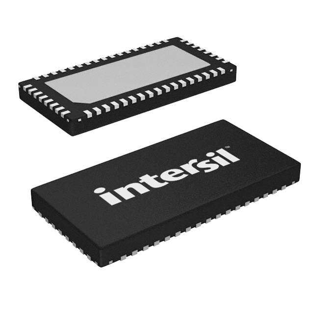
| 产品图片 |
|
| rohs | 符合RoHS无铅 / 符合限制有害物质指令(RoHS)规范要求 |
| 产品系列 | 电源管理 IC,稳压器—开关式稳压器,Microchip Technology MCP1640T-I/CHY- |
| 数据手册 | http://www.microchip.com/mymicrochip/filehandler.aspx?ddocname=en547085http://www.microchip.com/mymicrochip/filehandler.aspx?ddocname=en550216 |
| 产品型号 | MCP1640T-I/CHY |
| PCN组件/产地 | http://www.microchip.com/mymicrochip/NotificationDetails.aspx?id=5526&print=viewhttp://www.microchip.com/mymicrochip/NotificationDetails.aspx?id=5683&print=view |
| PWM类型 | - |
| 产品种类 | 稳压器—开关式稳压器 |
| 供应商器件封装 | SOT-23-6 |
| 其它名称 | MCP1640T-I/CHYDKR |
| 包装 | Digi-Reel® |
| 参考设计库 | http://www.digikey.com/rdl/4294959904/4294959903/519http://www.digikey.com/rdl/4294959904/4294959903/486http://www.digikey.com/rdl/4294959904/4294959903/564 |
| 同步整流器 | 是 |
| 商标 | Microchip Technology |
| 安装类型 | 表面贴装 |
| 安装风格 | SMD/SMT |
| 封装 | Reel |
| 封装/外壳 | SOT-23-6 |
| 封装/箱体 | SOT-23-6 |
| 工作温度 | -40°C ~ 85°C |
| 工作温度范围 | - 40 C to + 85 C |
| 工厂包装数量 | 3000 |
| 开关频率 | 500 kHz |
| 拓扑结构 | Boost |
| 最大工作温度 | + 85 C |
| 最大输入电压 | 5.5 V |
| 最小工作温度 | - 40 C |
| 最小输入电压 | 0.35 V |
| 标准包装 | 1 |
| 特色产品 | http://www.digikey.com/cn/zh/ph/Microchip/mcp1640-boost-regulator.html |
| 电压-输入 | 0.8 V ~ 5.5 V |
| 电压-输出 | 2 V ~ 5.5 V |
| 电流-输出 | 100mA |
| 电源电压-最小 | 0.35 V |
| 类型 | 升压(升压) |
| 系列 | MCP1640 |
| 负载调节 | 0.01 % |
| 输出数 | 1 |
| 输出电压 | 2 V to 5.5 V |
| 输出电流 | 350 mA |
| 输出端数量 | 1 Output |
| 输出类型 | 可调式 |
| 频率-开关 | 500kHz |


- 商务部:美国ITC正式对集成电路等产品启动337调查
- 曝三星4nm工艺存在良率问题 高通将骁龙8 Gen1或转产台积电
- 太阳诱电将投资9.5亿元在常州建新厂生产MLCC 预计2023年完工
- 英特尔发布欧洲新工厂建设计划 深化IDM 2.0 战略
- 台积电先进制程称霸业界 有大客户加持明年业绩稳了
- 达到5530亿美元!SIA预计今年全球半导体销售额将创下新高
- 英特尔拟将自动驾驶子公司Mobileye上市 估值或超500亿美元
- 三星加码芯片和SET,合并消费电子和移动部门,撤换高东真等 CEO
- 三星电子宣布重大人事变动 还合并消费电子和移动部门
- 海关总署:前11个月进口集成电路产品价值2.52万亿元 增长14.8%


PDF Datasheet 数据手册内容提取
MCP1640/B/C/D 0.65V Start-up Synchronous Boost Regulator with True Output Disconnect or Input/Output Bypass Option Features General Description • Up to 96% Typical Efficiency The MCP1640/B/C/D is a compact, high-efficiency, • 800mA Typical Peak Input Current Limit: fixed frequency, synchronous step-up DC-DC con- verter. It provides an easy-to-use power supply solution - I > 100mA @ 1.2V V , 3.3V V OUT IN OUT for applications powered by either one-cell, two-cell, or - I > 350mA @ 2.4V V , 3.3V V OUT IN OUT three-cell alkaline, NiCd, NiMH, one-cell Li-Ion or - I > 350mA @ 3.3V V 5.0V V OUT IN, OUT Li-Polymer batteries. • Low Start-up Voltage: 0.65V, typical 3.3V V OUT Low-voltage technology allows the regulator to start up @ 1mA without high inrush current or output voltage overshoot • Low Operating Input Voltage: 0.35V, typical from a low 0.65V input. High efficiency is accomplished 3.3V @ 1mA OUT by integrating the low resistance N-Channel Boost • Adjustable Output Voltage Range: 2.0V to 5.5V switch and synchronous P-Channel switch. All • Maximum Input Voltage V < 5.5V compensation and protection circuitry are integrated to OUT • Automatic PFM/PWM Operation (MCP1640/C): minimize external components. For standby applications, the MCP1640 operates and consumes - PFM Operation Disabled (MCP1640B/D) only 19µA while operating at no load and provides a - PWM Operation: 500kHz true disconnect from input to output while shut down • Low Device Quiescent Current: 19µA, typical (EN=GND). Additional device options are available PFM Mode that operate in PWM only mode and connect input to • Internal Synchronous Rectifier output bypass while shut down. • Internal Compensation A “true” load disconnect mode provides input to output • Inrush Current Limiting and Internal Soft-Start isolation while disabled by removing the normal boost • Selectable, Logic Controlled, Shutdown States: regulator diode path from input to output. A bypass mode option connects the input to the output using the - True Load Disconnect Option (MCP1640/B) integrated low resistance P-Channel MOSFET, which - Input to Output Bypass Option (MCP1640C/D) provides a low bias keep alive voltage for circuits • Shutdown Current (All States): < 1µA operating in Deep Sleep mode. Both options consume • Low Noise, Anti-Ringing Control less than 1µA of input current. • Overtemperature Protection Output voltage is set by a small external resistor • Available Packages: divider. Two package options, SOT23-6 and 2x3 - SOT23-6 DFN-8, are available. - 2x3 8-Lead DFN Package Types Applications MCP1640 MCP1640 • One, Two and Three Cell Alkaline and NiMH/NiCd 6-Lead SOT23 2x3DFN* Portable Products • Single Cell Li-Ion to 5V Converters SW 1 6 VIN VFB 1 8 VIN • Li Coin Cell Powered Devices GND 2 5 VOUT SGND 2 EP 7 VOUTS • Personal Medical Products PGND 3 9 6 VOUTP • Wireless Sensors EN 3 4 VFB EN 4 5 SW • Handheld Instruments • GPS Receivers * Includes Exposed Thermal Pad (EP); see Table3-1. • Bluetooth Headsets • +3.3V to +5.0V Distributed Power Supply 2010 Microchip Technology Inc. DS22234A-page 1
MCP1640/B/C/D L 1 4.7µH V OUT VIN SW 3.3V@100mA 0.9VTo1.7V VOUT V IN 976K + CIN COUT E 4.7µF EN VFB 10µF N LI A 562K K L A- GND L 1 4.7µH V OUT VIN SW 5.0V@300mA 3.0VTo4.2V VOUTS V IN V OUTP 976K + CIN COUT 4.7µF EN VFB 10µF N O -I 309K LI - PGNDSGND Efficiency vs. I for 3.3V OUT OUT 100.0 V = 2.5V IN %) 80.0 ( y c n e ci VIN = 0.8V VIN = 1.2V Effi 60.0 40.0 0.1 1.0 10.0 100.0 1000.0 Output Current (mA) DS22234A-page 2 2010 Microchip Technology Inc.
MCP1640/B/C/D 1.0 ELECTRICAL † Notice: Stresses above those listed under “Maximum CHARACTERISTICS Ratings” may cause permanent damage to the device. This is a stress rating only and functional operation of Absolute Maximum Ratings † the device at those or any other conditions above those indicated in the operational sections of this EN, FB, VIN, VSW, VOUT - GND...........................+6.5V specification is not intended. Exposure to maximum EN, FB...........<greater of V or V > (GND - 0.3V) rating conditions for extended periods may affect OUT IN Output Short Circuit Current.......................Continuous device reliability. Output Current Bypass Mode...........................400mA Power Dissipation ............................Internally Limited Storage Temperature.........................-65oC to +150oC Ambient Temp. with Power Applied......-40oC to +85oC Operating Junction Temperature........-40oC to +125oC ESD Protection On All Pins: HBM........................................................3kV MM........................................................300V DC CHARACTERISTICS Electrical Characteristics: Unless otherwise indicated, V = 1.2V, C = C = 10µF, L = 4.7µH, V =3.3V, I =15mA, IN OUT IN OUT OUT T = +25°C. A Boldface specifications apply over the T range of -40oC to +85oC. A Parameters Sym Min Typ Max Units Conditions Input Characteristics Minimum Start-Up Voltage V — 0.65 0.8 V Note1 IN Minimum Input Voltage After V — 0.35 — V Note1 IN Start-Up Output Voltage Adjust Range V 2.0 5.5 V V V ; Note2 OUT OUT IN Maximum Output Current I 150 — mA 1.2V V , 2.0V V OUT IN OUT 100 150 — mA 1.5V V , 3.3V V IN OUT 350 — mA 3.3V V , 5.0V V IN OUT Feedback Voltage V 1.175 1.21 1.245 V — FB Feedback Input Bias Current I — 10 — pA — VFB Quiescent Current – PFM I — 19 30 µA Measured at V = 4.0V; QPFM OUT Mode EN = V , I = 0mA; IN OUT Note3 Quiescent Current – PWM I — 220 — µA Measured at V ; EN = V QPWM OUT IN Mode I = 0mA; Note3 OUT Quiescent Current – Shutdown I — 0.7 2.3 µA V =EN= GND; QSHDN OUT Includes N-Channel and P-Channel Switch Leakage NMOS Switch Leakage I — 0.3 1 µA V =V =5V; V = NLK IN SW OUT 5.5V V =V =GND EN FB PMOS Switch Leakage I — 0.05 0.2 µA V =VS =GND; PLK IN W V =5.5V OUT NMOS Switch ON Resistance R — 0.6 — V = 3.3V, I = 100mA DS(ON)N IN SW PMOS Switch ON Resistance R — 0.9 — V = 3.3V, I = 100mA DS(ON)P IN SW Note 1: 3.3K resistive load, 3.3V (1mA). OUT 2: For V > V , V will not remain in regulation. IN OUT OUT 3: I is measured from V ; V quiescent current will vary with boost ratio. V quiescent current can be Q OUT IN IN estimated by: (I * (V /V )), (I * (V /V )). QPFM OUT IN QPWM OUT IN 4: 220 resistive load, 3.3V (15mA). OUT 5: Peak current limit determined by characterization, not production tested. 2010 Microchip Technology Inc. DS22234A-page 3
MCP1640/B/C/D DC CHARACTERISTICS (CONTINUED) Electrical Characteristics: Unless otherwise indicated, V = 1.2V, C = C = 10µF, L = 4.7µH, V =3.3V, I =15mA, IN OUT IN OUT OUT T = +25°C. A Boldface specifications apply over the T range of -40oC to +85oC. A Parameters Sym Min Typ Max Units Conditions NMOS Peak Switch Current I 600 850 — mA Note5 N(MAX) Limit V Accuracy V % -3 — +3 % Includes Line and Load OUT OUT Regulation; V = 1.5V IN Line Regulation V / -1 0.01 1 %/V V = 1.5V to 3V OUT IN V ) / I = 25mA OUT OUT V | IN Load Regulation V / -1 0.01 1 % I = 25mA to 100mA; OUT OUT V | V = 1.5V OUT IN Maximum Duty Cycle DC 88 90 — % MAX Switching Frequency f 425 500 575 kHz SW EN Input Logic High VIH 90 — — %of VIN IOUT = 1mA EN Input Logic Low VIL — — 20 %of VIN IOUT = 1mA EN Input Leakage Current I — 0.005 — µA V = 5V ENLK EN Soft-start Time t — 750 — µS EN Low to High, 90% of SS V ; Note4 OUT Thermal Shutdown Die T — 150 — C SD Temperature Die Temperature Hysteresis T — 10 — C SDHYS Note 1: 3.3K resistive load, 3.3V (1mA). OUT 2: For V > V , V will not remain in regulation. IN OUT OUT 3: I is measured from V ; V quiescent current will vary with boost ratio. V quiescent current can be Q OUT IN IN estimated by: (I * (V /V )), (I * (V /V )). QPFM OUT IN QPWM OUT IN 4: 220 resistive load, 3.3V (15mA). OUT 5: Peak current limit determined by characterization, not production tested. TEMPERATURE SPECIFICATIONS Electrical Specifications: Parameters Sym Min Typ Max Units Conditions Temperature Ranges Operating Junction Temperature T -40 — +125 °C Steady State J Range Storage Temperature Range T -65 — +150 °C A Maximum Junction Temperature T — — +150 °C Transient J Package Thermal Resistances Thermal Resistance, 5L-TSOT23 — 192 — °C/W EIA/JESD51-3 Standard JA Thermal Resistance, 8L-2x3 DFN — 93 — °C/W JA DS22234A-page 4 2010 Microchip Technology Inc.
MCP1640/B/C/D 2.0 TYPICAL PERFORMANCE CURVES Note: The graphs and tables provided following this note are a statistical summary based on a limited number of samples and are provided for informational purposes only. The performance characteristics listed herein are not tested or guaranteed. In some graphs or tables, the data presented may be outside the specified operating range (e.g., outside specified power supply range) and therefore outside the warranted range. Note: Unless otherwise indicated, V =EN=1.2V, C =C =10µF, L=4.7µH, V =3.3V, I =15mA, T =+25°C. IN OUT IN OUT LOAD A 27.5 100 VOUT = 2.0V VIN = 1.6V 25.0 VIN = 1.2V VOUT = 5.0V 90 80 A) Mode (µ 2202..05 VOUT = 3.3V ency (%) 567000 VIN = 0.8V VIN = 1.2V M 17.5 ci 40 PFQ15.0 VOUT = 2.0V Effi 30 PWM / PFM I 20 12.5 PWM ONLY 10 10.0 0 -40 -25 -10 5 20 35 50 65 80 0.01 0.1 1 10 100 1000 Ambient Temperature (°C) IOUT (mA) FIGURE 2-1: V I vs. Ambient FIGURE 2-4: 2.0V V PFM / PWM OUT Q OUT Temperature in PFM Mode. Mode Efficiency vs. I . OUT 300 100 VOUT = 3.3V VIN = 2.5V VOUT = 5.0V 90 275 VIN = 1.2V 80 M Mode (µA) 222550 VOUT = 3.3V ciency (%) 45670000 VIN = 0.8V VIN = 1.2V PW 200 Effi 30 PWM / PFM Q 20 I 175 PWM ONLY 10 150 0 -40 -25 -10 5 20 35 50 65 80 0.01 0.1 1 10 100 1000 Ambient Temperature (°C) IOUT (mA) FIGURE 2-2: V I vs. Ambient FIGURE 2-5: 3.3V V PFM / PWM OUT Q OUT Temperature in PWM Mode. Mode Efficiency vs. I . OUT 600 VOUT = 5.0V 10900 VOUT = 5.0V VIN = 2.5V 500 VOUT = 3.3V 80 400 %) 70 VIN = 1.2V VIN = 1.8V (mA)OUT300 VOUT = 2.0V ciency ( 456000 I 200 Effi 30 PWM / PFM 100 20 PWM ONLY 10 0 0 0 0.5 1 1.5 2 2.5 3 3.5 4 4.5 5 0.01 0.1 1 10 100 1000 VIN (V) IOUT (mA) FIGURE 2-3: Maximum I vs. V . FIGURE 2-6: 5.0V V PFM / PWM OUT IN OUT Mode Efficiency vs. I . OUT 2010 Microchip Technology Inc. DS22234A-page 5
MCP1640/B/C/D Note: Unless otherwise indicated, V =EN=1.2V, C =C =10µF, L=4.7µH, V =3.3V, I =15mA, T =+25°C. IN OUT IN OUT LOAD A 3.33.2353 IOUT = 15 mA VIN = 1.2V 1.00 VOUT = 3.3V 3.32 0.85 3.315 VIN = 1.8V Startup V (V)OUT3.33.0351 V (V)IN00..5750 3.3 Shutdown 3.295 VIN = 0.8V 0.40 3.29 3.285 0.25 -40 -25 -10 5 20 35 50 65 80 0 20 40 60 80 100 Ambient Temperature (°C) IOUT (mA) FIGURE 2-7: 3.3V V vs. Ambient FIGURE 2-10: Minimum Start-up and OUT Temperature. Shutdown V into Resistive Load vs. I . IN OUT 3.38 525 VIN = 1.5V Hz)520 VOUT = 3.3V 3.36 k 3.34 IOUT = 5 mA ncy (551105 V (V)OUT33..3302 ng Freque455900505 IOUT = 15 mA chi490 3.28 IOUT = 50 mA Swit485 3.26 480 -40 -25 -10 5 20 35 50 65 80 -40 -25 -10 5 20 35 50 65 80 Ambient Temperature (°C) Ambient Temperature (°C) FIGURE 2-8: 3.3V V vs. Ambient FIGURE 2-11: F vs. Ambient OUT OSC Temperature. Temperature. 3.40 4.5 TA = 85°C IOUT = 5 mA 4 VOUT = 5.0V 3.36 3.5 3 V (V)OUT33..2382 TA = 25°C V (V)IN2.25 VOUT = 3.3VVOUT = 2.0V TA = - 40°C 1.5 3.24 1 0.5 3.20 0 0.8 1.2 1.6 2 2.4 2.8 0 1 2 3 4 5 6 7 8 9 10 V (V) I (mA) IN OUT FIGURE 2-9: 3.3V V vs. V . FIGURE 2-12: PWM Pulse Skipping Mode OUT IN Threshold vs. I . OUT DS22234A-page 6 2010 Microchip Technology Inc.
MCP1640/B/C/D Note: Unless otherwise indicated, V =EN=1.2V, C =C =10µF, L=4.7µH, V =3.3V, I =15mA, T =+25°C. IN OUT IN OUT LOAD A 10000 PWM / PFM PWM ONLY 1000 VOUT = 5.0V A) µ I (IN VOUT = 2.0V VOUT = 3.3V 100 VOUT = 2.0V VOUT = 3.3V VOUT = 5.0V 10 0.8 1.1 1.4 1.7 2 2.3 2.6 2.9 3.2 3.5 V (V) IN FIGURE 2-13: Input No Load Current vs. FIGURE 2-16: MCP1640 3.3V V PFM OUT V . Mode Waveforms. IN 5 s) m h 4 O e ( P - Channel nc 3 a st si 2 e R h c 1 wit S N - Channel 0 1 1.5 2 2.5 3 3.5 4 4.5 5 > V or V IN OUT FIGURE 2-14: N-Channel and P-Channel FIGURE 2-17: MCP1640B 3.3V V OUT R vs. > of V or V . PWM Mode Waveforms. DSON IN OUT 16 VOUT = 5.0V 14 VOUT = 2.0V VOUT = 3.3V 12 A) 10 m (UT 8 IO 6 4 2 0 0 0.5 1 1.5 2 2.5 3 3.5 4 V (V) IN FIGURE 2-15: PFM / PWM Threshold FIGURE 2-18: MCP1640/B High Load Current vs. V . Waveforms. IN 2010 Microchip Technology Inc. DS22234A-page 7
MCP1640/B/C/D Note: Unless otherwise indicated, V =EN=1.2V, C =C =10µF, L=4.7µH, V =3.3V, I =15mA, T =+25°C. IN OUT IN OUT LOAD A FIGURE 2-19: 3.3V Start-up After Enable. FIGURE 2-22: MCP1640B 3.3V V Load OUT Transient Waveforms. FIGURE 2-20: 3.3V Start-up when V = FIGURE 2-23: MCP1640B 2.0V V Load IN OUT V . Transient Waveforms. ENABLE FIGURE 2-21: MCP1640 3.3V V Load FIGURE 2-24: 3.3V V Line Transient OUT OUT Transient Waveforms. Waveforms. DS22234A-page 8 2010 Microchip Technology Inc.
MCP1640/B/C/D 3.0 PIN DESCRIPTIONS The descriptions of the pins are listed in Table3-1. TABLE 3-1: PIN FUNCTION TABLE MCP1640/B/C/D MCP1640/B/C/D Pin No. Description SOT23 2x3 DFN SW 1 5 Switch Node, Boost Inductor Input Pin GND 2 Ground Pin EN 3 4 Enable Control Input Pin FB 4 1 Feedback Voltage Pin V 5 Output Voltage Pin OUT V 6 8 Input Voltage Pin IN S 2 Signal Ground Pin GND P 3 Power Ground Pin GND V 7 Output Voltage Sense Pin OUTS V 6 Output Voltage Power Pin OUTP EP — 9 Exposed Thermal Pad (EP); must be connected to V SS. 3.1 Switch Node Pin (SW) 3.6 Power Supply Input Voltage Pin (V ) Connect the inductor from the input voltage to the SW IN pin. The SW pin carries inductor current and can be as Connect the input voltage source to V . The input IN high as 800mA peak. The integrated N-Channel switch source should be decoupled to GND with a 4.7µF drain and integrated P-Channel switch source are inter- minimum capacitor. nally connected at the SW node. 3.7 Signal Ground Pin (S ) GND 3.2 Ground Pin (GND) The signal ground pin is used as a return for the integrated V and error amplifier. In the 2x3 DFN REF The ground or return pin is used for circuit ground con- package, the S and power ground (P ) pins are GND GND nection. Length of trace from input cap return, output connected externally. cap return and GND pin should be made as short as possible to minimize noise on the GND pin. In the 3.8 Power Ground Pin (PGND) SOT23-6 package, a single ground pin is used. The power ground pin is used as a return for the high- current N-Channel switch. In the 2x3 DFN package, the 3.3 Enable Pin (EN) P and signal ground (S ) pins are connected GND GND externally. The EN pin is a logic-level input used to enable or disable device switching and lower quiescent current 3.9 Output Voltage Sense Pin (V ) OUTS while disabled. A logic high (>90% of V ) will enable IN The output voltage sense pin connects the regulated the regulator output. A logic low (<20% of V ) will IN output voltage to the internal bias circuits. In the 2x3 ensure that the regulator is disabled. DFN package, V and V are connected OUTS OUTP externally. 3.4 Feedback Voltage Pin (FB) 3.10 Output Voltage Power Pin (V ) The FB pin is used to provide output voltage regulation OUTP by using a resistor divider. The FB voltage will be 1.21V The output voltage power pin connects the output volt- typical with the output voltage in regulation. age to the switch node. High current flows through the integrated P-Channel and out of this pin to the output 3.5 Output Voltage Pin (VOUT) capacitor and output. In the 2x3 DFN package, VOUTS and V are connected externally. OUTP The output voltage pin connects the integrated 3.11 Exposed Thermal Pad (EP) P-Channel MOSFET to the output capacitor. The FB voltage divider is also connected to the VOUT pin for There is no internal electrical connection between the voltage regulation. Exposed Thermal Pad (EP) and the P and S GND GND pins. They must be connected to the same potential on the Printed Circuit Board (PCB). 2010 Microchip Technology Inc. DS22234A-page 9
MCP1640/B/C/D NOTES: DS22234A-page 10 2010 Microchip Technology Inc.
MCP1640/B/C/D 4.0 DETAILED DESCRIPTION 4.1.3 TRUE OUTPUT DISCONNECT OPTION 4.1 Device Option Overview The MCP1640/B devices incorporate a true output disconnect feature. With the EN pin pulled low, the The MCP1640/B/C/D family of devices is capable of output of the MCP1640/B is isolated or disconnected low start-up voltage and delivers high efficiency over a from the input by turning off the integrated P-Channel wide load range for single cell, two cell, three cell switch and removing the switch bulk diode connection. alkaline, NiMH, NiCd and single cell Li-Ion battery This removes the DC path typical in boost converters, inputs. A high level of integration lowers total system which allows the output to be disconnected from the cost, eases implementation and reduces board area. input. During this mode, less than 1µA of current is The devices feature low start-up voltage, adjustable consumed from the input (battery). True output discon- output voltage, PWM/PFM mode operation, low I , Q nect does not discharge the output; the output voltage integrated synchronous switch, internal compensation, is held up by the external C capacitance. low noise anti-ring control, inrush current limit and soft OUT start. There are two feature options for the MCP1640/ 4.1.4 INPUT BYPASS OPTION B/C/D family: PWM/PFM mode or PWM mode only, and “true output disconnect” or input bypass. The MCP1640C/D devices incorporate the input bypass shutdown option. With the EN input pulled low, 4.1.1 PWM/PFM MODE OPTION the output is connected to the input using the internal P-Channel MOSFET. In this mode, the current draw The MCP1640/C devices use an automatic switchover from the input (battery) is less than 1µA with no load. from PWM to PFM mode for light load conditions to The Input Bypass mode is used when the input voltage maximize efficiency over a wide range of output range is high enough for the load to operate in Sleep or current. During PFM mode, higher peak current is used low I mode. When a higher regulated output voltage is to pump the output up to the threshold limit. While Q necessary to operate the application, the EN input is operating in PFM or PWM mode, the P-Channel switch pulled high enabling the boost converter. is used as a synchronous rectifier, turning off when the inductor current reaches 0 mA to maximize efficiency. TABLE 4-1: PART NUMBER SELECTION In PFM mode, a comparator is used to terminate Part PWM/ switching when the output voltage reaches the upper PWM True Dis Bypass Number PFM threshold limit. Once switching has terminated, the output voltage will decay or coast down. During this MCP1640 X X period, very low I is consumed from the device and Q MCP1640B X X input source, which keeps power efficiency high at light load. The disadvantages of PWM/PFM mode are MCP1640C X X higher output ripple voltage and variable PFM mode MCP1640D X X frequency. The PFM mode frequency is a function of input voltage, output voltage and load. While in PFM mode, the boost converter pumps the output up at a switching frequency of 500kHz. 4.1.2 PWM MODE ONLY OPTION The MCP1640B/D devices disable PFM mode switching, and operate only in PWM mode over the entire load range. During periods of light load opera- tion, the MCP1640B/D continues to operate at a con- stant 500kHz switching frequency keeping the output ripple voltage lower than PFM mode. During PWM only mode, the MCP1640B/D P-Channel switch acts as a synchronous rectifier by turning off to prevent reverse current flow from the output cap back to the input in order to keep efficiency high. For noise immunity, the N-Channel MOSFET current sense is blanked for approximately 100ns. With a typical minimum duty cycle of 100ns, the MCP1640B/D continues to switch at a constant frequency under light load conditions. Figure2-12 represents the input voltage versus load current for the pulse skipping threshold in PWM only mode. At lighter loads, the MCP1640B/D devices begin to skip pulses. 2010 Microchip Technology Inc. DS22234A-page 11
MCP1640/B/C/D 4.2 Functional Description Figure 4-1 depicts the functional block diagram of the MCP1640/B/C/D. The MCP1640/B/C/D is a compact, high-efficiency, fixed frequency, step-up DC-DC converter that provides an easy-to-use power supply solution for applications powered by either one-cell, two-cell, or three-cell alkaline, NiCd, or NiMH, or one-cell Li-Ion or Li-Polymer batteries. VOUT INTERNAL VIN BIAS IZERO DIRECTION CONTROL SW SOFT-START .3V GATE DRIVE 0V AND ILIMIT SHUTDOWN EN CONTROL LOGIC ISENSE GND OSCILLATOR SLOPE COMP. PWM/PFM LOGIC 1.21V FB EA FIGURE 4-1: MCP1640/B/C/D Block Diagram. 4.2.1 LOW-VOLTAGE START-UP 50% of its nominal value. Once the output voltage reaches 1.6V, normal closed-loop PWM operation is The MCP1640/B/C/D is capable of starting from a low initiated. input voltage. Start-up voltage is typically 0.65V for a 3.3V output and 1mA resistive load. The MCP1640/B/C/D charges an internal capacitor with a very weak current source. The voltage on this When enabled, the internal start-up logic turns the capacitor, in turn, slowly ramps the current limit of the rectifying P-Channel switch on until the output boost switch to its nominal value. The soft-start capacitor is charged to a value close to the input capacitor is completely discharged in the event of a voltage. The rectifying switch is current limited during commanded shutdown or a thermal shutdown. this time. After charging the output capacitor to the input voltage, the device starts switching. If the input There is no undervoltage lockout feature for the voltage is below 1.6V, the device runs open-loop with a MCP1640/B/C/D. The device will start up at the lowest fixed duty cycle of 70% until the output reaches 1.6V. possible voltage and run down to the lowest possible During this time, the boost switch current is limited to voltage. For typical battery applications, this may result in “motor-boating” for deeply discharged batteries. DS22234A-page 12 2010 Microchip Technology Inc.
MCP1640/B/C/D 4.2.2 PWM MODE OPERATION 4.2.6 INTERNAL BIAS In normal PWM operation, the MCP1640/B/C/D The MCP1640/B/C/D gets its start-up bias from V . IN operates as a fixed frequency, synchronous boost Once the output exceeds the input, bias comes from converter. The switching frequency is internally the output. Therefore, once started, operation is maintained with a precision oscillator typically set to completely independent of V . Operation is only IN 500kHz. The MCP1640B/D devices will operate in limited by the output power level and the input source PWM only mode even during periods of light load series resistance. Once started, the output will remain operation. By operating in PWM only mode, the output in regulation down to 0.35V typical with 1mA output ripple remains low and the frequency is constant. current for low source impedance inputs. Operating in fixed PWM mode results in lower efficiency during light load operation (when compared 4.2.7 INTERNAL COMPENSATION to PFM mode (MCP1640/C)). The error amplifier, with its associated compensation Lossless current sensing converts the peak current sig- network, completes the closed loop system by nal to a voltage to sum with the internal slope compen- comparing the output voltage to a reference at the sation. This summed signal is compared to the voltage input of the error amplifier, and feeding the amplified error amplifier output to provide a peak current control and inverted signal to the control input of the inner command for the PWM signal. The slope current loop. The compensation network provides compensation is adaptive to the input and output phase leads and lags at appropriate frequencies to voltage. Therefore, the converter provides the proper cancel excessive phase lags and leads of the power amount of slope compensation to ensure stability, but is circuit. All necessary compensation components and not excessive, which causes a loss of phase margin. slope compensation are integrated. The peak current limit is set to 800mA typical. 4.2.8 SHORT CIRCUIT PROTECTION 4.2.3 PFM MODE OPERATION Unlike most boost converters, the MCP1640/B/C/D The MCP1640/C devices are capable of operating in allows its output to be shorted during normal operation. normal PWM mode and PFM mode to maintain high The internal current limit and overtemperature efficiency at all loads. In PFM mode, the output ripple protection limit excessive stress and protect the device has a variable frequency component that changes with during periods of short circuit, overcurrent and over- the input voltage and output current. With no load, the temperature. While operating in Bypass mode, the quiescent current draw from the output is typically P-Channel current limit is inhibited to minimize 19µA. The PFM mode can be disabled in selected quiescent current. device options. 4.2.9 LOW NOISE OPERATION PFM operation is initiated if the output load current falls below an internally programmed threshold. The output The MCP1640/B/C/D integrates a low noise anti-ring voltage is continuously monitored. When the output switch that damps the oscillations typically observed at voltage drops below its nominal value, PFM operation the switch node of a boost converter when operating in pulses one or several times to bring the output back the discontinuous inductor current mode. This removes into regulation. If the output load current rises above the high frequency radiated noise. the upper threshold, the MCP1640/C transitions 4.2.10 OVERTEMPERATURE smoothly into PWM mode. PROTECTION 4.2.4 ADJUSTABLE OUTPUT VOLTAGE Overtemperature protection circuitry is integrated in the The MCP1640/B/C/D output voltage is adjustable with MCP1640/B/C/D. This circuitry monitors the device a resistor divider over a 2.0V minimum to 5.5V junction temperature and shuts the device off if the maximum range. High value resistors are junction temperature exceeds the typical +150oC recommended to minimize quiescent current to keep threshold. If this threshold is exceeded, the device will efficiency high at light loads. automatically restart once the junction temperature drops by 10oC. The soft start is reset during an 4.2.5 ENABLE overtemperature condition. The enable pin is used to turn the boost converter on and off. The enable threshold voltage varies with input voltage. To enable the boost converter, the EN voltage level must be greater than 90% of the V voltage. To IN disable the boost converter, the EN voltage must be less than 20% of the V voltage. IN 2010 Microchip Technology Inc. DS22234A-page 13
MCP1640/B/C/D NOTES: DS22234A-page 14 2010 Microchip Technology Inc.
MCP1640/B/C/D 5.0 APPLICATION INFORMATION 5.3 Input Capacitor Selection The boost input current is smoothed by the boost 5.1 Typical Applications inductor reducing the amount of filtering necessary at the input. Some capacitance is recommended to The MCP1640/B/C/D synchronous boost regulator provide decoupling from the source. Low ESR X5R or operates over a wide input voltage and output voltage X7R are well suited since they have a low temperature range. The power efficiency is high for several decades coefficient and small size. For most applications, of load range. Output current capability increases with 4.7µF of capacitance is sufficient at the input. For high input voltage and decreases with increasing output power applications that have high source impedance or voltage. The maximum output current is based on the long leads, connecting the battery to the input 10µF of N-Channel peak current limit. Typical characterization capacitance is recommended. Additional input curves in this data sheet are presented to display the capacitance can be added to provide a stable input typical output current capability. voltage. 5.2 Adjustable Output Voltage Table5-1 contains the recommended range for the Calculations input capacitor value. To calculate the resistor divider values for the 5.4 Output Capacitor Selection MCP1640/B/C/D, the following equation can be used. Where R is connected to V , R is connected The output capacitor helps provide a stable output TOP OUT BOT to GND and both are connected to the FB input pin. voltage during sudden load transients and reduces the output voltage ripple. As with the input capacitor, X5R EQUATION 5-1: and X7R ceramic capacitors are well suited for this application. V R = R ----O----U---T-- –1 The MCP1640/B/C/D is internally compensated so TOP BOT V output capacitance range is limited. See Table5-1 for FB the recommended output capacitor range. Example A: While the N-Channel switch is on, the output current is supplied by the output capacitor C . The amount of OUT V = 3.3V OUT output capacitance and equivalent series resistance V = 1.21V will have a significant effect on the output ripple FB voltage. While C provides load current, a voltage R = 309k OUT BOT drop also appears across its internal ESR that results RTOP = 533.7k (Standard Value = 536k) in ripple voltage. Example B: EQUATION 5-2: V = 5.0V OUT VFB = 1.21V dV I = C ------- RBOT = 309k OUT OUT dt R = 967.9k (Standard Value = 976k) TOP There are some potential issues with higher value Where dV represents the ripple voltage and dt resistors. For small surface mount resistors, represents the ON time of the N-Channel switch (D * 1/ environment contamination can create leakage paths FSW). that significantly change the resistor divider that effect Table5-1 contains the recommended range for the the output voltage. The FB input leakage current can input and output capacitor value. also impact the divider and change the output voltage tolerance. TABLE 5-1: CAPACITOR VALUE RANGE C C IN OUT Min 4.7µF 10µF Max none 100µF 2010 Microchip Technology Inc. DS22234A-page 15
MCP1640/B/C/D 5.5 Inductor Selection Peak current is the maximum or limit, and saturation current typically specifies a point at which the induc- The MCP1640/B/C/D is designed to be used with small tance has rolled off a percentage of the rated value. surface mount inductors; the inductance value can This can range from a 20% to 40% reduction in induc- range from 2.2µH to 10µH. An inductance value of tance. As inductance rolls off, the inductor ripple cur- 4.7µH is recommended to achieve a good balance rent increases as does the peak switch current. It is between inductor size, converter load transient important to keep the inductance from rolling off too response and minimized noise. much, causing switch current to reach the peak limit. TABLE 5-2: MCP1640/B/C/D 5.6 Thermal Calculations RECOMMENDED INDUCTORS Part Value DCR I Size The MCP1640/B/C/D is available in two different SAT Number (µH) (typ) (A) WxLxH (mm) packages (SOT23-6 and 2x3 DFN8). By calculating the power dissipation and applying the package thermal Coiltronics® resistance,( ), the junction temperature is esti- JA SD3110 4.7 0.285 0.68 3.1x3.1x1.0 mated. The maximum continuous junction temperature SD3112 4.7 0.246 0.80 3.1x3.1x1.2 rating for the MCP1640/B/C/D is +125oC. SD3114 4.7 0.251 1.14 3.1x3.1x1.4 To quickly estimate the internal power dissipation for SD3118 4.7 0.162 1.31 3.8x3.8x1.2 the switching boost regulator, an empirical calculation using measured efficiency can be used. Given the SD3812 4.7 0.256 1.13 3.8x3.8x1.2 measured efficiency, the internal power dissipation is SD25 4.7 0.0467 1.83 5.0x5.0x2.5 estimated by Equation5-3. DCR Part Value I Size SAT EQUATION 5-3: Number (µH) (A) WxLxH (mm) (max) Wurth Elektronik® V I OUT OUT ------------------------------- –V I = P WE-TPC 4.7 0.200 0.8 2.8x2.8x1.35 Efficiency OUT OUT Dis Type TH WE-TPC 4.7 0.105 0.90 3.8x3.8x1.65 Type S The difference between the first term, input power, and WE-TPC 4.7 0.082 1.65 4.8x4.8x1.8 the second term, power delivered, is the internal Type M MCP1640/B/C/D power dissipation. This is an estimate WE-TPC 4.7 0.046 2.00 6.8x6.8x2.3 assuming that most of the power lost is internal to the Type X MCP1640/B/C/D and not C , C and the inductor. IN OUT There is some percentage of power lost in the boost DCR Part Value ISAT Size inductor, with very little loss in the input and output Number (µH) (A) WxLxH (mm) capacitors. For a more accurate estimation of internal (max) power dissipation, subtract the I 2*L power INRMS ESR Sumida® dissipation. CMH23 4.7 0.537 0.70 2.3x2.3x1.0 5.7 PCB Layout Information CMD4D06 4.7 0.216 0.75 3.5x4.3x0.8 CDRH4D 4.7 0.09 0.800 4.6x4.6x1.5 Good printed circuit board layout techniques are EPCOS® important to any switching circuitry and switching power supplies are no different. When wiring the B82462A2 4.7 0.084 2.00 6.0x6.0x2.5 switching high current paths, short and wide traces 472M000 should be used. Therefore it is important that the input B82462G4 4.7 0.04 1.8 6.3x6.3x3.0 and output capacitors be placed as close as possible to 472M the MCP1640/B/C/D to minimize the loop area. Several parameters are used to select the correct The feedback resistors and feedback signal should be inductor: maximum rated current, saturation current routed away from the switching node and the switching and copper resistance (ESR). For boost converters, the current loop. When possible, ground planes and traces inductor current can be much higher than the output should be used to help shield the feedback signal and current. The lower the inductor ESR, the higher the minimize noise and magnetic interference. efficiency of the converter, a common trade-off in size versus efficiency. DS22234A-page 16 2010 Microchip Technology Inc.
MCP1640/B/C/D Via to GND Plane R R BOT TOP +V +V IN OUT C C L IN MCP1640 OUT 1 GND GND Via for Enable FIGURE 5-1: MCP1640/B/C/D SOT23-6 Recommended Layout. Wired on Bottom L Plane +V IN +V OUT C C IN OUT GND MCP1640 R TOP 1 R BOT Enable GND FIGURE 5-2: MCP1640/B/C/D DFN-8 Recommended Layout. 2010 Microchip Technology Inc. DS22234A-page 17
MCP1640/B/C/D NOTES: DS22234A-page 18 2010 Microchip Technology Inc.
MCP1640/B/C/D 6.0 TYPICAL APPLICATION CIRCUITS L 1 4.7µH V OUT MANGANESE LITHIUM 5.0V@5mA DIOXIDE BUTTON CELL SW V OUT V IN + 976K 2.0V TO 3.2V CIN COUT - 4.7µF EN VFB 10µF 309K FROM PIC® MCU I/O GND Note: For applications that can operate directly from the battery input voltage during Sleep mode and require a higher voltage during normal run mode, the MCP1640C device provides input to output bypass when disabled. The PIC Microcontroller is powered by the output of the MCP1640C. One of its I/O pins is used to enable and disable the MCP1640C to control its bias voltage. While operating in Sleep mode, the MCP1640C input quiescent current is typically less than 1 uA. FIGURE 6-1: Manganese Lithium Coin Cell Application using Bypass Mode. L 1 10µH V OUT VIN SW 5.0V@350mA 3.3VTo4.2V VOUTS V IN V OUTP 976K + CIN COUT 10µF EN VFB 10µF N O -I 309K LI - PGNDSGND FIGURE 6-2: USB On-The-Go Powered by Li-Ion. 2010 Microchip Technology Inc. DS22234A-page 19
MCP1640/B/C/D NOTES: DS22234A-page 20 2010 Microchip Technology Inc.
MCP1640/B/C/D 7.0 PACKAGING INFORMATION 7.1 Package Marking Information (Not to Scale) 6-Lead SOT-23 Example XXNN BZNN 8-Lead DFN Example XXX AHM YWW 945 NN 25 Legend: XX...X Customer-specific information Y Year code (last digit of calendar year) YY Year code (last 2 digits of calendar year) WW Week code (week of January 1 is week ‘01’) NNN Alphanumeric traceability code e3 Pb-free JEDEC designator for Matte Tin (Sn) * This package is Pb-free. The Pb-free JEDEC designator ( e 3 ) can be found on the outer packaging for this package. Note: In the event the full Microchip part number cannot be marked on one line, it will be carried over to the next line, thus limiting the number of available characters for customer-specific information. 2010 Microchip Technology Inc. DS22234A-page 21
MCP1640/B/C/D (cid:2)(cid:3)(cid:4)(cid:5)(cid:6)(cid:7)(cid:8)(cid:9)(cid:10)(cid:6)(cid:11)(cid:12)(cid:13)(cid:14)(cid:8)(cid:15)(cid:16)(cid:6)(cid:10)(cid:10)(cid:8)(cid:17)(cid:18)(cid:12)(cid:10)(cid:13)(cid:19)(cid:5)(cid:8)(cid:20)(cid:21)(cid:6)(cid:19)(cid:11)(cid:13)(cid:11)(cid:12)(cid:22)(cid:21)(cid:8)(cid:23)(cid:24)(cid:25)(cid:26)(cid:8)(cid:27)(cid:15)(cid:17)(cid:20)(cid:3)(cid:28)(cid:29)(cid:30) (cid:31)(cid:22)(cid:12)(cid:5) /(cid:23)(cid:22)(cid:14)$(cid:24)(cid:13)(cid:14) (cid:23)!$(cid:14)(cid:21)%(cid:22)(cid:22)(cid:13)(cid:26)$(cid:14)(cid:10)(cid:11)(cid:21)0(cid:11)(cid:12)(cid:13)(cid:14)"(cid:22)(cid:11).(cid:20)(cid:26)(cid:12)!1(cid:14)(cid:10)(cid:27)(cid:13)(cid:11)!(cid:13)(cid:14)!(cid:13)(cid:13)(cid:14)$(cid:24)(cid:13)(cid:14)(cid:19)(cid:20)(cid:21)(cid:22)(cid:23)(cid:21)(cid:24)(cid:20)(cid:10)(cid:14)2(cid:11)(cid:21)0(cid:11)(cid:12)(cid:20)(cid:26)(cid:12)(cid:14)(cid:3)(cid:10)(cid:13)(cid:21)(cid:20)&(cid:20)(cid:21)(cid:11)$(cid:20)(cid:23)(cid:26)(cid:14)(cid:27)(cid:23)(cid:21)(cid:11)$(cid:13)"(cid:14)(cid:11)$(cid:14) (cid:24)$$(cid:10),33...(cid:30) (cid:20)(cid:21)(cid:22)(cid:23)(cid:21)(cid:24)(cid:20)(cid:10)(cid:30)(cid:21)(cid:23) 3(cid:10)(cid:11)(cid:21)0(cid:11)(cid:12)(cid:20)(cid:26)(cid:12) b N 4 E E1 PIN1IDBY LASERMARK 1 2 3 e e1 D A A2 c φ L A1 L1 4(cid:26)(cid:20)$! (cid:19)(cid:29)55(cid:29)(cid:19)#(cid:25)#(cid:8)(cid:3) (cid:2)(cid:20) (cid:13)(cid:26)!(cid:20)(cid:23)(cid:26)(cid:14)5(cid:20) (cid:20)$! (cid:19)(cid:29)6 67(cid:19) (cid:19)(cid:7)8 6% 9(cid:13)(cid:22)(cid:14)(cid:23)&(cid:14)2(cid:20)(cid:26)! 6 (cid:16) 2(cid:20)$(cid:21)(cid:24) (cid:13) (cid:4)(cid:30)(cid:6))(cid:14)*(cid:3)+ 7%$!(cid:20)"(cid:13)(cid:14)5(cid:13)(cid:11)"(cid:14)2(cid:20)$(cid:21)(cid:24) (cid:13)(cid:31) (cid:31)(cid:30)(cid:6)(cid:4)(cid:14)*(cid:3)+ 7-(cid:13)(cid:22)(cid:11)(cid:27)(cid:27)(cid:14):(cid:13)(cid:20)(cid:12)(cid:24)$ (cid:7) (cid:4)(cid:30)(cid:6)(cid:4) ; (cid:31)(cid:30)(cid:5)) (cid:19)(cid:23)(cid:27)"(cid:13)"(cid:14)2(cid:11)(cid:21)0(cid:11)(cid:12)(cid:13)(cid:14)(cid:25)(cid:24)(cid:20)(cid:21)0(cid:26)(cid:13)!! (cid:7)(cid:17) (cid:4)(cid:30)<(cid:6) ; (cid:31)(cid:30)(cid:15)(cid:4) (cid:3)$(cid:11)(cid:26)"(cid:23)&& (cid:7)(cid:31) (cid:4)(cid:30)(cid:4)(cid:4) ; (cid:4)(cid:30)(cid:31)) 7-(cid:13)(cid:22)(cid:11)(cid:27)(cid:27)(cid:14)=(cid:20)"$(cid:24) # (cid:17)(cid:30)(cid:17)(cid:4) ; (cid:15)(cid:30)(cid:17)(cid:4) (cid:19)(cid:23)(cid:27)"(cid:13)"(cid:14)2(cid:11)(cid:21)0(cid:11)(cid:12)(cid:13)(cid:14)=(cid:20)"$(cid:24) #(cid:31) (cid:31)(cid:30)(cid:15)(cid:4) ; (cid:31)(cid:30)<(cid:4) 7-(cid:13)(cid:22)(cid:11)(cid:27)(cid:27)(cid:14)5(cid:13)(cid:26)(cid:12)$(cid:24) (cid:2) (cid:17)(cid:30)(cid:18)(cid:4) ; (cid:15)(cid:30)(cid:31)(cid:4) /(cid:23)(cid:23)$(cid:14)5(cid:13)(cid:26)(cid:12)$(cid:24) 5 (cid:4)(cid:30)(cid:31)(cid:4) ; (cid:4)(cid:30)(cid:16)(cid:4) /(cid:23)(cid:23)$(cid:10)(cid:22)(cid:20)(cid:26)$ 5(cid:31) (cid:4)(cid:30)(cid:15)) ; (cid:4)(cid:30)<(cid:4) /(cid:23)(cid:23)$(cid:14)(cid:7)(cid:26)(cid:12)(cid:27)(cid:13) (cid:3) (cid:4)> ; (cid:15)(cid:4)> 5(cid:13)(cid:11)"(cid:14)(cid:25)(cid:24)(cid:20)(cid:21)0(cid:26)(cid:13)!! (cid:21) (cid:4)(cid:30)(cid:4)< ; (cid:4)(cid:30)(cid:17)(cid:16) 5(cid:13)(cid:11)"(cid:14)=(cid:20)"$(cid:24) 9 (cid:4)(cid:30)(cid:17)(cid:4) ; (cid:4)(cid:30))(cid:31) (cid:31)(cid:22)(cid:12)(cid:5)(cid:11) (cid:31)(cid:30) (cid:2)(cid:20) (cid:13)(cid:26)!(cid:20)(cid:23)(cid:26)!(cid:14)(cid:2)(cid:14)(cid:11)(cid:26)"(cid:14)#(cid:31)(cid:14)"(cid:23)(cid:14)(cid:26)(cid:23)$(cid:14)(cid:20)(cid:26)(cid:21)(cid:27)%"(cid:13)(cid:14) (cid:23)(cid:27)"(cid:14)&(cid:27)(cid:11)!(cid:24)(cid:14)(cid:23)(cid:22)(cid:14)(cid:10)(cid:22)(cid:23)$(cid:22)%!(cid:20)(cid:23)(cid:26)!(cid:30)(cid:14)(cid:19)(cid:23)(cid:27)"(cid:14)&(cid:27)(cid:11)!(cid:24)(cid:14)(cid:23)(cid:22)(cid:14)(cid:10)(cid:22)(cid:23)$(cid:22)%!(cid:20)(cid:23)(cid:26)!(cid:14)!(cid:24)(cid:11)(cid:27)(cid:27)(cid:14)(cid:26)(cid:23)$(cid:14)(cid:13)’(cid:21)(cid:13)(cid:13)"(cid:14)(cid:4)(cid:30)(cid:31)(cid:17)(cid:18)(cid:14) (cid:14)(cid:10)(cid:13)(cid:22)(cid:14)!(cid:20)"(cid:13)(cid:30) (cid:17)(cid:30) (cid:2)(cid:20) (cid:13)(cid:26)!(cid:20)(cid:23)(cid:26)(cid:20)(cid:26)(cid:12)(cid:14)(cid:11)(cid:26)"(cid:14)$(cid:23)(cid:27)(cid:13)(cid:22)(cid:11)(cid:26)(cid:21)(cid:20)(cid:26)(cid:12)(cid:14)(cid:10)(cid:13)(cid:22)(cid:14)(cid:7)(cid:3)(cid:19)#(cid:14)((cid:31)(cid:5)(cid:30))(cid:19)(cid:30) *(cid:3)+, *(cid:11)!(cid:20)(cid:21)(cid:14)(cid:2)(cid:20) (cid:13)(cid:26)!(cid:20)(cid:23)(cid:26)(cid:30)(cid:14)(cid:25)(cid:24)(cid:13)(cid:23)(cid:22)(cid:13)$(cid:20)(cid:21)(cid:11)(cid:27)(cid:27)(cid:28)(cid:14)(cid:13)’(cid:11)(cid:21)$(cid:14)-(cid:11)(cid:27)%(cid:13)(cid:14)!(cid:24)(cid:23).(cid:26)(cid:14).(cid:20)$(cid:24)(cid:23)%$(cid:14)$(cid:23)(cid:27)(cid:13)(cid:22)(cid:11)(cid:26)(cid:21)(cid:13)!(cid:30) (cid:19)(cid:20)(cid:21)(cid:22)(cid:23)(cid:21)(cid:24)(cid:20)(cid:10)(cid:25)(cid:13)(cid:21)(cid:24)(cid:26)(cid:23)(cid:27)(cid:23)(cid:12)(cid:28)(cid:2)(cid:22)(cid:11).(cid:20)(cid:26)(cid:12)+(cid:4)(cid:5)(cid:9)(cid:4)(cid:17)<* DS22234A-page 22 2010 Microchip Technology Inc.
MCP1640/B/C/D Note: For the most current package drawings, please see the Microchip Packaging Specification located at http://www.microchip.com/packaging 2010 Microchip Technology Inc. DS22234A-page 23
MCP1640/B/C/D !(cid:3)(cid:4)(cid:5)(cid:6)(cid:7)(cid:8)(cid:9)(cid:10)(cid:6)(cid:11)(cid:12)(cid:13)(cid:14)(cid:8)"(cid:18)(cid:6)(cid:10)(cid:8)#(cid:10)(cid:6)(cid:12)$(cid:8)(cid:31)(cid:22)(cid:8)(cid:4)(cid:5)(cid:6)(cid:7)(cid:8)(cid:9)(cid:6)(cid:14)%(cid:6)&(cid:5)(cid:8)(cid:23)’(cid:24)(cid:26)(cid:8)((cid:8)(cid:28))(cid:29))*+,(cid:8)(cid:16)(cid:16)(cid:8)-(cid:22)(cid:7).(cid:8)(cid:27)"#(cid:31)(cid:30) (cid:31)(cid:22)(cid:12)(cid:5) /(cid:23)(cid:22)(cid:14)$(cid:24)(cid:13)(cid:14) (cid:23)!$(cid:14)(cid:21)%(cid:22)(cid:22)(cid:13)(cid:26)$(cid:14)(cid:10)(cid:11)(cid:21)0(cid:11)(cid:12)(cid:13)(cid:14)"(cid:22)(cid:11).(cid:20)(cid:26)(cid:12)!1(cid:14)(cid:10)(cid:27)(cid:13)(cid:11)!(cid:13)(cid:14)!(cid:13)(cid:13)(cid:14)$(cid:24)(cid:13)(cid:14)(cid:19)(cid:20)(cid:21)(cid:22)(cid:23)(cid:21)(cid:24)(cid:20)(cid:10)(cid:14)2(cid:11)(cid:21)0(cid:11)(cid:12)(cid:20)(cid:26)(cid:12)(cid:14)(cid:3)(cid:10)(cid:13)(cid:21)(cid:20)&(cid:20)(cid:21)(cid:11)$(cid:20)(cid:23)(cid:26)(cid:14)(cid:27)(cid:23)(cid:21)(cid:11)$(cid:13)"(cid:14)(cid:11)$(cid:14) (cid:24)$$(cid:10),33...(cid:30) (cid:20)(cid:21)(cid:22)(cid:23)(cid:21)(cid:24)(cid:20)(cid:10)(cid:30)(cid:21)(cid:23) 3(cid:10)(cid:11)(cid:21)0(cid:11)(cid:12)(cid:20)(cid:26)(cid:12) D e b N N L K E E2 EXPOSEDPAD NOTE1 NOTE1 1 2 2 1 D2 TOPVIEW BOTTOMVIEW A NOTE2 A3 A1 4(cid:26)(cid:20)$! (cid:19)(cid:29)55(cid:29)(cid:19)#(cid:25)#(cid:8)(cid:3) (cid:2)(cid:20) (cid:13)(cid:26)!(cid:20)(cid:23)(cid:26)(cid:14)5(cid:20) (cid:20)$! (cid:19)(cid:29)6 67(cid:19) (cid:19)(cid:7)8 6% 9(cid:13)(cid:22)(cid:14)(cid:23)&(cid:14)2(cid:20)(cid:26)! 6 < 2(cid:20)$(cid:21)(cid:24) (cid:13) (cid:4)(cid:30))(cid:4)(cid:14)*(cid:3)+ 7-(cid:13)(cid:22)(cid:11)(cid:27)(cid:27)(cid:14):(cid:13)(cid:20)(cid:12)(cid:24)$ (cid:7) (cid:4)(cid:30)<(cid:4) (cid:4)(cid:30)(cid:6)(cid:4) (cid:31)(cid:30)(cid:4)(cid:4) (cid:3)$(cid:11)(cid:26)"(cid:23)&&(cid:14) (cid:7)(cid:31) (cid:4)(cid:30)(cid:4)(cid:4) (cid:4)(cid:30)(cid:4)(cid:17) (cid:4)(cid:30)(cid:4)) +(cid:23)(cid:26)$(cid:11)(cid:21)$(cid:14)(cid:25)(cid:24)(cid:20)(cid:21)0(cid:26)(cid:13)!! (cid:7)(cid:15) (cid:4)(cid:30)(cid:17)(cid:4)(cid:14)(cid:8)#/ 7-(cid:13)(cid:22)(cid:11)(cid:27)(cid:27)(cid:14)5(cid:13)(cid:26)(cid:12)$(cid:24) (cid:2) (cid:17)(cid:30)(cid:4)(cid:4)(cid:14)*(cid:3)+ 7-(cid:13)(cid:22)(cid:11)(cid:27)(cid:27)(cid:14)=(cid:20)"$(cid:24) # (cid:15)(cid:30)(cid:4)(cid:4)(cid:14)*(cid:3)+ #’(cid:10)(cid:23)!(cid:13)"(cid:14)2(cid:11)"(cid:14)5(cid:13)(cid:26)(cid:12)$(cid:24) (cid:2)(cid:17) (cid:31)(cid:30)(cid:15)(cid:4) ; (cid:31)(cid:30))) #’(cid:10)(cid:23)!(cid:13)"(cid:14)2(cid:11)"(cid:14)=(cid:20)"$(cid:24) #(cid:17) (cid:31)(cid:30))(cid:4) ; (cid:31)(cid:30)(cid:18)) +(cid:23)(cid:26)$(cid:11)(cid:21)$(cid:14)=(cid:20)"$(cid:24) 9 (cid:4)(cid:30)(cid:17)(cid:4) (cid:4)(cid:30)(cid:17)) (cid:4)(cid:30)(cid:15)(cid:4) +(cid:23)(cid:26)$(cid:11)(cid:21)$(cid:14)5(cid:13)(cid:26)(cid:12)$(cid:24) 5 (cid:4)(cid:30)(cid:15)(cid:4) (cid:4)(cid:30)(cid:5)(cid:4) (cid:4)(cid:30))(cid:4) +(cid:23)(cid:26)$(cid:11)(cid:21)$(cid:9)$(cid:23)(cid:9)#’(cid:10)(cid:23)!(cid:13)"(cid:14)2(cid:11)" ? (cid:4)(cid:30)(cid:17)(cid:4) ; ; (cid:31)(cid:22)(cid:12)(cid:5)(cid:11) (cid:31)(cid:30) 2(cid:20)(cid:26)(cid:14)(cid:31)(cid:14)-(cid:20)!%(cid:11)(cid:27)(cid:14)(cid:20)(cid:26)"(cid:13)’(cid:14)&(cid:13)(cid:11)$%(cid:22)(cid:13)(cid:14) (cid:11)(cid:28)(cid:14)-(cid:11)(cid:22)(cid:28)1(cid:14)9%$(cid:14) %!$(cid:14)9(cid:13)(cid:14)(cid:27)(cid:23)(cid:21)(cid:11)$(cid:13)"(cid:14).(cid:20)$(cid:24)(cid:20)(cid:26)(cid:14)$(cid:24)(cid:13)(cid:14)(cid:24)(cid:11)$(cid:21)(cid:24)(cid:13)"(cid:14)(cid:11)(cid:22)(cid:13)(cid:11)(cid:30) (cid:17)(cid:30) 2(cid:11)(cid:21)0(cid:11)(cid:12)(cid:13)(cid:14) (cid:11)(cid:28)(cid:14)(cid:24)(cid:11)-(cid:13)(cid:14)(cid:23)(cid:26)(cid:13)(cid:14)(cid:23)(cid:22)(cid:14) (cid:23)(cid:22)(cid:13)(cid:14)(cid:13)’(cid:10)(cid:23)!(cid:13)"(cid:14)$(cid:20)(cid:13)(cid:14)9(cid:11)(cid:22)!(cid:14)(cid:11)$(cid:14)(cid:13)(cid:26)"!(cid:30) (cid:15)(cid:30) 2(cid:11)(cid:21)0(cid:11)(cid:12)(cid:13)(cid:14)(cid:20)!(cid:14)!(cid:11).(cid:14)!(cid:20)(cid:26)(cid:12)%(cid:27)(cid:11)$(cid:13)"(cid:30) (cid:5)(cid:30) (cid:2)(cid:20) (cid:13)(cid:26)!(cid:20)(cid:23)(cid:26)(cid:20)(cid:26)(cid:12)(cid:14)(cid:11)(cid:26)"(cid:14)$(cid:23)(cid:27)(cid:13)(cid:22)(cid:11)(cid:26)(cid:21)(cid:20)(cid:26)(cid:12)(cid:14)(cid:10)(cid:13)(cid:22)(cid:14)(cid:7)(cid:3)(cid:19)#(cid:14)((cid:31)(cid:5)(cid:30))(cid:19)(cid:30) *(cid:3)+, *(cid:11)!(cid:20)(cid:21)(cid:14)(cid:2)(cid:20) (cid:13)(cid:26)!(cid:20)(cid:23)(cid:26)(cid:30)(cid:14)(cid:25)(cid:24)(cid:13)(cid:23)(cid:22)(cid:13)$(cid:20)(cid:21)(cid:11)(cid:27)(cid:27)(cid:28)(cid:14)(cid:13)’(cid:11)(cid:21)$(cid:14)-(cid:11)(cid:27)%(cid:13)(cid:14)!(cid:24)(cid:23).(cid:26)(cid:14).(cid:20)$(cid:24)(cid:23)%$(cid:14)$(cid:23)(cid:27)(cid:13)(cid:22)(cid:11)(cid:26)(cid:21)(cid:13)!(cid:30) (cid:8)#/, (cid:8)(cid:13)&(cid:13)(cid:22)(cid:13)(cid:26)(cid:21)(cid:13)(cid:14)(cid:2)(cid:20) (cid:13)(cid:26)!(cid:20)(cid:23)(cid:26)1(cid:14)%!%(cid:11)(cid:27)(cid:27)(cid:28)(cid:14).(cid:20)$(cid:24)(cid:23)%$(cid:14)$(cid:23)(cid:27)(cid:13)(cid:22)(cid:11)(cid:26)(cid:21)(cid:13)1(cid:14)&(cid:23)(cid:22)(cid:14)(cid:20)(cid:26)&(cid:23)(cid:22) (cid:11)$(cid:20)(cid:23)(cid:26)(cid:14)(cid:10)%(cid:22)(cid:10)(cid:23)!(cid:13)!(cid:14)(cid:23)(cid:26)(cid:27)(cid:28)(cid:30) (cid:19)(cid:20)(cid:21)(cid:22)(cid:23)(cid:21)(cid:24)(cid:20)(cid:10)(cid:25)(cid:13)(cid:21)(cid:24)(cid:26)(cid:23)(cid:27)(cid:23)(cid:12)(cid:28)(cid:2)(cid:22)(cid:11).(cid:20)(cid:26)(cid:12)+(cid:4)(cid:5)(cid:9)(cid:31)(cid:17)(cid:15)+ DS22234A-page 24 2010 Microchip Technology Inc.
MCP1640/B/C/D !(cid:3)(cid:4)(cid:5)(cid:6)(cid:7)(cid:8)(cid:9)(cid:10)(cid:6)(cid:11)(cid:12)(cid:13)(cid:14)(cid:8)"(cid:18)(cid:6)(cid:10)(cid:8)#(cid:10)(cid:6)(cid:12)$(cid:8)(cid:31)(cid:22)(cid:8)(cid:4)(cid:5)(cid:6)(cid:7)(cid:8)(cid:9)(cid:6)(cid:14)%(cid:6)&(cid:5)(cid:8)(cid:23)’(cid:24)(cid:26)(cid:8)((cid:8)(cid:28))(cid:29))*+,(cid:8)(cid:16)(cid:16)(cid:8)-(cid:22)(cid:7).(cid:8)(cid:27)"#(cid:31)(cid:30) (cid:31)(cid:22)(cid:12)(cid:5) /(cid:23)(cid:22)(cid:14)$(cid:24)(cid:13)(cid:14) (cid:23)!$(cid:14)(cid:21)%(cid:22)(cid:22)(cid:13)(cid:26)$(cid:14)(cid:10)(cid:11)(cid:21)0(cid:11)(cid:12)(cid:13)(cid:14)"(cid:22)(cid:11).(cid:20)(cid:26)(cid:12)!1(cid:14)(cid:10)(cid:27)(cid:13)(cid:11)!(cid:13)(cid:14)!(cid:13)(cid:13)(cid:14)$(cid:24)(cid:13)(cid:14)(cid:19)(cid:20)(cid:21)(cid:22)(cid:23)(cid:21)(cid:24)(cid:20)(cid:10)(cid:14)2(cid:11)(cid:21)0(cid:11)(cid:12)(cid:20)(cid:26)(cid:12)(cid:14)(cid:3)(cid:10)(cid:13)(cid:21)(cid:20)&(cid:20)(cid:21)(cid:11)$(cid:20)(cid:23)(cid:26)(cid:14)(cid:27)(cid:23)(cid:21)(cid:11)$(cid:13)"(cid:14)(cid:11)$(cid:14) (cid:24)$$(cid:10),33...(cid:30) (cid:20)(cid:21)(cid:22)(cid:23)(cid:21)(cid:24)(cid:20)(cid:10)(cid:30)(cid:21)(cid:23) 3(cid:10)(cid:11)(cid:21)0(cid:11)(cid:12)(cid:20)(cid:26)(cid:12) 2010 Microchip Technology Inc. DS22234A-page 25
MCP1640/B/C/D NOTES: DS22234A-page 26 2010 Microchip Technology Inc.
MCP1640/B/C/D APPENDIX A: REVISION HISTORY Revision A (February 2010) • Original Release of this Document. 2010 Microchip Technology Inc. DS22234A-page 27
MCP1640/B/C/D NOTES: DS22234A-page 28 2010 Microchip Technology Inc.
MCP1640/B/C/D PRODUCT IDENTIFICATION SYSTEM To order or obtain information, e.g., on pricing or delivery, refer to the factory or the listed sales office. PART NO. X X /XX Examples: Device Tape Temperature Package a) MCP1640-I/MC: 0.65V, Sync Reg., and Reel Range 8LD-DFN pkg. b) MCP1640T-I/MC: Tape and Reel, 0.65V, Sync Reg., Device MCP1640: 0.65V, PWM/PFM True Disconnect, 8LD-DFN pkg. Sync Boost Regulator MCP1640T: 0.65V, PWM/PFM True Disconnect, c) MCP1640B-I/MC: 0.65V, Sync Reg., Sync Boost Regulator (Tape and Reel) 8LD-DFN pkg. MCP1640B: 0.65V, PWM Only True Disconnect, d) MCP1640BT-I/MC: Tape and Reel, Sync Boost Regulator MCP1640BT: 0.65V, PWM Only True Disconnect, 0.65V, Sync Reg., Sync Boost Regulator (Tape and Reel) 8LD-DFN pkg. MCP1640C: 0.65V, PWM/PFM Input to Output Bypass, Sync Boost Regulator e) MCP1640C-I/MC: 0.65V, Sync Reg., MCP1640CT: 0.65V, PWM/PFM Input to Output Bypass, 8LD-DFN pkg. Sync Boost Regulator (Tape and Reel) f) MCP1640CT-I/MC: Tape and Reel, MCP1640D: 0.65V, PWM Only Input to Output Bypass, 0.65V, Sync Reg., Sync Boost Regulator 8LD-DFN pkg. MCP1640DT: 0.65V, PWM Only Input to Output Bypass, Sync Boost Regulator (Tape and Reel) g) MCP1640D-I/MC:: 0.65V, Sync Reg., 8LD-DFN pkg. Temperature Range I = -40C to +85C (Industrial) h) MCP1640DT-I/MC:: Tape and Reel, 0.65V, Sync Reg., 8LD-DFN pkg. Package CH = Plastic Small Outline Transistor (SOT-23), 6-lead MC = Plastic Dual Flat, No Lead (2x3 DFN), 8-lead i) MCP1640T-I/CHY: Tape and Reel, 0.65V, Sync Reg., 6LD SOT-23 pkg. j) MCP1640BT-I/CHY: Tape and Reel, 0.65V, Sync Reg., 6LD SOT-23 pkg. k) MCP1640CT-I/CHY: Tape and Reel, 0.65V, Sync Reg., 6LD SOT-23 pkg. l) MCP1640DT-I/CHY: Tape and Reel, 0.65V, Sync Reg., 6LD SOT-23 pkg. 2010 Microchip Technology Inc. DS22234A-page 29
MCP1640/B/C/D NOTES: DS22234A-page 30 2010 Microchip Technology Inc.
Note the following details of the code protection feature on Microchip devices: • Microchip products meet the specification contained in their particular Microchip Data Sheet. • Microchip believes that its family of products is one of the most secure families of its kind on the market today, when used in the intended manner and under normal conditions. • There are dishonest and possibly illegal methods used to breach the code protection feature. All of these methods, to our knowledge, require using the Microchip products in a manner outside the operating specifications contained in Microchip’s Data Sheets. Most likely, the person doing so is engaged in theft of intellectual property. • Microchip is willing to work with the customer who is concerned about the integrity of their code. • Neither Microchip nor any other semiconductor manufacturer can guarantee the security of their code. Code protection does not mean that we are guaranteeing the product as “unbreakable.” Code protection is constantly evolving. We at Microchip are committed to continuously improving the code protection features of our products. Attempts to break Microchip’s code protection feature may be a violation of the Digital Millennium Copyright Act. If such acts allow unauthorized access to your software or other copyrighted work, you may have a right to sue for relief under that Act. Information contained in this publication regarding device Trademarks applications and the like is provided only for your convenience The Microchip name and logo, the Microchip logo, dsPIC, and may be superseded by updates. It is your responsibility to KEELOQ, KEELOQ logo, MPLAB, PIC, PICmicro, PICSTART, ensure that your application meets with your specifications. rfPIC and UNI/O are registered trademarks of Microchip MICROCHIP MAKES NO REPRESENTATIONS OR Technology Incorporated in the U.S.A. and other countries. WARRANTIES OF ANY KIND WHETHER EXPRESS OR IMPLIED, WRITTEN OR ORAL, STATUTORY OR FilterLab, Hampshire, HI-TECH C, Linear Active Thermistor, OTHERWISE, RELATED TO THE INFORMATION, MXDEV, MXLAB, SEEVAL and The Embedded Control INCLUDING BUT NOT LIMITED TO ITS CONDITION, Solutions Company are registered trademarks of Microchip QUALITY, PERFORMANCE, MERCHANTABILITY OR Technology Incorporated in the U.S.A. FITNESS FOR PURPOSE. Microchip disclaims all liability Analog-for-the-Digital Age, Application Maestro, CodeGuard, arising from this information and its use. Use of Microchip dsPICDEM, dsPICDEM.net, dsPICworks, dsSPEAK, ECAN, devices in life support and/or safety applications is entirely at ECONOMONITOR, FanSense, HI-TIDE, In-Circuit Serial the buyer’s risk, and the buyer agrees to defend, indemnify and Programming, ICSP, Mindi, MiWi, MPASM, MPLAB Certified hold harmless Microchip from any and all damages, claims, logo, MPLIB, MPLINK, mTouch, Octopus, Omniscient Code suits, or expenses resulting from such use. No licenses are Generation, PICC, PICC-18, PICDEM, PICDEM.net, PICkit, conveyed, implicitly or otherwise, under any Microchip PICtail, PIC32 logo, REAL ICE, rfLAB, Select Mode, Total intellectual property rights. Endurance, TSHARC, UniWinDriver, WiperLock and ZENA are trademarks of Microchip Technology Incorporated in the U.S.A. and other countries. SQTP is a service mark of Microchip Technology Incorporated in the U.S.A. All other trademarks mentioned herein are property of their respective companies. © 2010, Microchip Technology Incorporated, Printed in the U.S.A., All Rights Reserved. Printed on recycled paper. ISBN: 978-1-60932-019-5 Microchip received ISO/TS-16949:2002 certification for its worldwide headquarters, design and wafer fabrication facilities in Chandler and Tempe, Arizona; Gresham, Oregon and design centers in California and India. The Company’s quality system processes and procedures are for its PIC® MCUs and dsPIC® DSCs, KEELOQ® code hopping devices, Serial EEPROMs, microperipherals, nonvolatile memory and analog products. In addition, Microchip’s quality system for the design and manufacture of development systems is ISO 9001:2000 certified. 2010 Microchip Technology Inc. DS22234A-page 31
WORLDWIDE SALES AND SERVICE AMERICAS ASIA/PACIFIC ASIA/PACIFIC EUROPE Corporate Office Asia Pacific Office India - Bangalore Austria - Wels 2355 West Chandler Blvd. Suites 3707-14, 37th Floor Tel: 91-80-3090-4444 Tel: 43-7242-2244-39 Chandler, AZ 85224-6199 Tower 6, The Gateway Fax: 91-80-3090-4123 Fax: 43-7242-2244-393 Tel: 480-792-7200 Harbour City, Kowloon India - New Delhi Denmark - Copenhagen Fax: 480-792-7277 Hong Kong Tel: 91-11-4160-8631 Tel: 45-4450-2828 Technical Support: Tel: 852-2401-1200 Fax: 91-11-4160-8632 Fax: 45-4485-2829 http://support.microchip.com Web Address: Fax: 852-2401-3431 India - Pune France - Paris www.microchip.com Australia - Sydney Tel: 91-20-2566-1512 Tel: 33-1-69-53-63-20 Tel: 61-2-9868-6733 Fax: 91-20-2566-1513 Fax: 33-1-69-30-90-79 ADtullaunthta, GA Fax: 61-2-9868-6755 Japan - Yokohama Germany - Munich Tel: 678-957-9614 China - Beijing Tel: 81-45-471- 6166 Tel: 49-89-627-144-0 Tel: 86-10-8528-2100 Fax: 49-89-627-144-44 Fax: 678-957-1455 Fax: 81-45-471-6122 Fax: 86-10-8528-2104 Italy - Milan Boston Korea - Daegu Westborough, MA China - Chengdu Tel: 82-53-744-4301 Tel: 39-0331-742611 Tel: 774-760-0087 Tel: 86-28-8665-5511 Fax: 82-53-744-4302 Fax: 39-0331-466781 Fax: 774-760-0088 Fax: 86-28-8665-7889 Korea - Seoul Netherlands - Drunen Chicago China - Chongqing Tel: 82-2-554-7200 Tel: 31-416-690399 Itasca, IL Tel: 86-23-8980-9588 Fax: 82-2-558-5932 or Fax: 31-416-690340 Tel: 630-285-0071 Fax: 86-23-8980-9500 82-2-558-5934 Spain - Madrid Fax: 630-285-0075 China - Hong Kong SAR Malaysia - Kuala Lumpur Tel: 34-91-708-08-90 Cleveland Tel: 852-2401-1200 Tel: 60-3-6201-9857 Fax: 34-91-708-08-91 Independence, OH Fax: 852-2401-3431 Fax: 60-3-6201-9859 UK - Wokingham Tel: 216-447-0464 China - Nanjing Malaysia - Penang Tel: 44-118-921-5869 Fax: 216-447-0643 Tel: 86-25-8473-2460 Tel: 60-4-227-8870 Fax: 44-118-921-5820 Dallas Fax: 86-25-8473-2470 Fax: 60-4-227-4068 Addison, TX China - Qingdao Philippines - Manila Tel: 972-818-7423 Tel: 86-532-8502-7355 Tel: 63-2-634-9065 Fax: 972-818-2924 Fax: 86-532-8502-7205 Fax: 63-2-634-9069 Detroit China - Shanghai Singapore Farmington Hills, MI Tel: 86-21-5407-5533 Tel: 65-6334-8870 Tel: 248-538-2250 Fax: 86-21-5407-5066 Fax: 65-6334-8850 Fax: 248-538-2260 China - Shenyang Taiwan - Hsin Chu Kokomo Tel: 86-24-2334-2829 Tel: 886-3-6578-300 Kokomo, IN Fax: 86-24-2334-2393 Fax: 886-3-6578-370 Tel: 765-864-8360 Fax: 765-864-8387 China - Shenzhen Taiwan - Kaohsiung Tel: 86-755-8203-2660 Tel: 886-7-536-4818 Los Angeles Fax: 86-755-8203-1760 Fax: 886-7-536-4803 Mission Viejo, CA Tel: 949-462-9523 China - Wuhan Taiwan - Taipei Tel: 86-27-5980-5300 Tel: 886-2-2500-6610 Fax: 949-462-9608 Fax: 86-27-5980-5118 Fax: 886-2-2508-0102 Santa Clara China - Xian Thailand - Bangkok Santa Clara, CA Tel: 408-961-6444 Tel: 86-29-8833-7252 Tel: 66-2-694-1351 Fax: 408-961-6445 Fax: 86-29-8833-7256 Fax: 66-2-694-1350 China - Xiamen Toronto Mississauga, Ontario, Tel: 86-592-2388138 Canada Fax: 86-592-2388130 Tel: 905-673-0699 China - Zhuhai Fax: 905-673-6509 Tel: 86-756-3210040 Fax: 86-756-3210049 01/05/10 DS22234A-page 32 2010 Microchip Technology Inc.
Mouser Electronics Authorized Distributor Click to View Pricing, Inventory, Delivery & Lifecycle Information: M icrochip: MCP1640-I/MC MCP1640T-I/CHY MCP1640B-I/MC MCP1640BT-I/CHY MCP1640C-I/MC MCP1640CT-I/CHY MCP1640D-I/MC MCP1640DT-I/CHY