ICGOO在线商城 > 集成电路(IC) > PMIC - 栅极驱动器 > MCP14E4-E/SN

 Datasheet下载
- 型号: MCP14E4-E/SN
- 制造商: Microchip
- 库位|库存: xxxx|xxxx
- 要求:
| 数量阶梯 | 香港交货 | 国内含税 |
| +xxxx | $xxxx | ¥xxxx |
查看当月历史价格
查看今年历史价格
MCP14E4-E/SN产品简介:
ICGOO电子元器件商城为您提供MCP14E4-E/SN由Microchip设计生产,在icgoo商城现货销售,并且可以通过原厂、代理商等渠道进行代购。 MCP14E4-E/SN价格参考。MicrochipMCP14E4-E/SN封装/规格:PMIC - 栅极驱动器, Low-Side Gate Driver IC Non-Inverting 8-SOIC。您可以下载MCP14E4-E/SN参考资料、Datasheet数据手册功能说明书,资料中有MCP14E4-E/SN 详细功能的应用电路图电压和使用方法及教程。
MCP14E4-E/SN 是 Microchip Technology 公司生产的 PMIC(电源管理集成电路)系列中的栅极驱动器产品。其主要应用场景包括但不限于以下领域:

 1. 电机驱动
   - MCP14E4 可用于驱动 MOSFET 或 IGBT 等功率开关器件,广泛应用于直流无刷电机(BLDC)、步进电机和其他类型的电机控制系统中。
   - 在家电领域,如空调压缩机、洗衣机、冰箱风扇等需要高效能驱动的场景中,该器件能够提供稳定的栅极驱动信号。

 2. 电源转换
   - 在 DC-DC 转换器或 AC-DC 转换器中,MCP14E4 可以用作功率级驱动器,控制开关管的导通与关断,实现高效的电压调节。
   - 常见于适配器、充电器以及工业设备中的电源模块。

 3. 照明系统
   - LED 驱动电路中,MCP14E4 能够精确地控制功率晶体管,确保恒定电流输出,从而稳定 LED 的亮度。
   - 应用于路灯、汽车大灯和室内照明等场景。

 4. 太阳能逆变器
   - 在光伏逆变器中,MCP14E4 提供可靠的栅极驱动能力,支持 MPPT(最大功率点跟踪)算法下的高效能量转换。
   - 适用于小型家用太阳能发电系统及分布式能源解决方案。

 5. 工业自动化
   - 工业控制设备如可编程逻辑控制器(PLC)、伺服驱动器等需要高性能的功率驱动,MCP14E4 可满足这些需求。
   - 提供快速响应和低延迟特性,适合复杂运动控制环境。

 6. 消费电子产品
   - 在笔记本电脑、平板电脑以及其他便携式设备中,作为辅助驱动芯片,帮助优化电池续航并提高整体效率。

 特性优势:
- 支持高达 8A 的峰值驱动电流,适应多种功率等级的应用。
- 内置短路保护和过温关断功能,增强系统可靠性。
- 小型化封装设计(SOT-23),便于 PCB 布局和空间受限的设计。

综上所述,MCP14E4-E/SN 主要应用于需要高效功率控制和稳定驱动性能的各种电子设备中,覆盖工业、消费、汽车等多个领域。
| 参数 | 数值 |
| 产品目录 | 集成电路 (IC)半导体 |
| 描述 | IC MOSFET DVR 4.0A DUAL 8SOIC门驱动器 4.5A Dual MOSFET Driver |
| 产品分类 | PMIC - MOSFET,电桥驱动器 - 外部开关集成电路 - IC |
| 品牌 | Microchip Technology |
| 产品手册 | |
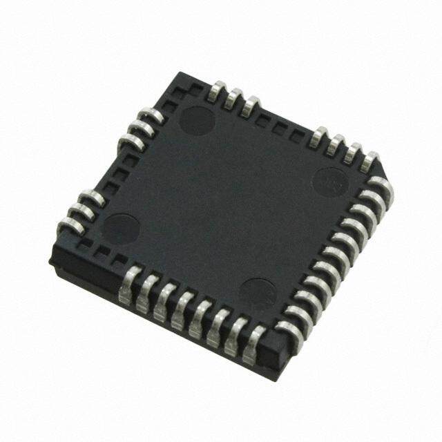
| 产品图片 |
|
| rohs | 符合RoHS无铅 / 符合限制有害物质指令(RoHS)规范要求 |
| 产品系列 | 电源管理 IC,门驱动器,Microchip Technology MCP14E4-E/SN- |
| 数据手册 | http://www.microchip.com/mymicrochip/filehandler.aspx?ddocname=en532049 |
| 产品型号 | MCP14E4-E/SN |
| PCN组件/产地 | http://www.microchip.com/mymicrochip/NotificationDetails.aspx?id=5774&print=view |
| PCN设计/规格 | http://www.microchip.com/mymicrochip/NotificationDetails.aspx?id=5704&print=view |
| 上升时间 | 15 ns |
| 下降时间 | 18 ns |
| 产品 | MOSFET Gate Drivers |
| 产品目录页面 | |
| 产品种类 | 门驱动器 |
| 供应商器件封装 | 8-SOIC N |
| 其它名称 | MCP14E4ESN |
| 包装 | 管件 |
| 商标 | Microchip Technology |
| 安装类型 | 表面贴装 |
| 安装风格 | SMD/SMT |
| 封装 | Tube |
| 封装/外壳 | 8-SOIC(0.154",3.90mm 宽) |
| 封装/箱体 | SOIC-8 |
| 工作温度 | -40°C ~ 125°C |
| 工厂包装数量 | 100 |
| 延迟时间 | 46ns |
| 最大功率耗散 | 665 mW |
| 最大工作温度 | + 125 C |
| 最小工作温度 | - 40 C |
| 标准包装 | 100 |
| 激励器数量 | 2 Driver |
| 电压-电源 | 4.5 V ~ 18 V |
| 电流-峰值 | 4A |
| 电源电压-最大 | 18 V |
| 电源电压-最小 | 4.5 V |
| 电源电流 | 0.75 mA |
| 类型 | Non-Inverting |
| 输入类型 | 非反相 |
| 输出数 | 2 |
| 输出电流 | 4 A |
| 输出端数量 | 2 |
| 配置 | Non-Inverting |
| 配置数 | 2 |
| 高压侧电压-最大值(自举) | - |


- 商务部:美国ITC正式对集成电路等产品启动337调查
- 曝三星4nm工艺存在良率问题 高通将骁龙8 Gen1或转产台积电
- 太阳诱电将投资9.5亿元在常州建新厂生产MLCC 预计2023年完工
- 英特尔发布欧洲新工厂建设计划 深化IDM 2.0 战略
- 台积电先进制程称霸业界 有大客户加持明年业绩稳了
- 达到5530亿美元!SIA预计今年全球半导体销售额将创下新高
- 英特尔拟将自动驾驶子公司Mobileye上市 估值或超500亿美元
- 三星加码芯片和SET,合并消费电子和移动部门,撤换高东真等 CEO
- 三星电子宣布重大人事变动 还合并消费电子和移动部门
- 海关总署:前11个月进口集成电路产品价值2.52万亿元 增长14.8%


PDF Datasheet 数据手册内容提取
MCP14E3/MCP14E4/MCP14E5 4.0A Dual High-Speed Power MOSFET Drivers With Enable Features General Description • High Peak Output Current: 4.0A (typical) The MCP14E3/MCP14E4/MCP14E5 devices are a • Independent Enable Function for Each Driver family of 4.0A buffers/MOSFET drivers. Dual-inverting, Output dual-noninvertering, and complementary outputs are standard logic options offered. • Low Shoot-Through/Cross-Conduction Current in Output Stage The MCP14E3/MCP14E4/MCP14E5 drivers are • Wide Input Supply Voltage Operating Range: capable of operating from a 4.5V to 18V single power supply and can easily charge and discharge 2200pF - 4.5V to 18V gate capacitance in under 15ns (typical). They provide • High Capacitive Load Drive Capability: low impedance in both the ON and OFF states to - 2200pF in 15ns (typical) ensure the MOSFET’s intended state will not be - 5600 pF in 26ns (typical) affected, even by large transients. The MCP14E3/ • Short Delay Times: 50ns (typical) MCP14E4/MCP14E5 inputs may be driven directly from either TTL or CMOS (2.4V to 18V). • Latch-Up Protected: Will Withstand 1.5A Reverse Current Additional control of the MCP14E3/MCP14E4/ • Logic Input Will Withstand Negative Swing Up To MCP14E5 outputs is allowed by the use of separate 5V enable functions. The ENB_A and ENB_B pins are • Space-Saving Packages: active high and are internally pulled up to VDD. The pins maybe left floating for standard operation. - 8-Lead 6x5 DFN, PDIP, SOIC The MCP14E3/MCP14E4/MCP14E5 dual-output 4.0A Applications driver family is offered in both surface-mount and pin- through-hole packages with a -40°C to +125°C • Switch Mode Power Supplies temperature rating. The low thermal resistance of the • Pulse Transformer Drive thermally enhanced DFN package allows for greater • Line Drivers power dissipation capability for driving heavier capacitive or resistive loads. • Motor and Solenoid Drive These devices are highly latch-up resistant under any conditions within their power and voltage ratings. They are not subject to damage when up to 5V of noise spiking (of either polarity) occurs on the ground pin. They can accept, without damage or logic upset, up to 1.5A of reverse current being forced back into their outputs. All terminals are fully protect against Electrostatic Discharge (ESD) up to 4kV. Package Types MCP14E4 8-Pin MCP14E4 8-Pin MCP14E3 MCP14E5 PDIP/SOIC MCP14E3 MCP14E5 6x5 DFN (1) ENB_A 1 8 ENB_B ENB_B ENB_B ENB_A 1 8 ENB_B ENB_B ENB_B IN A 2 7 OUT A OUT A OUT A IN A 2 7 OUT A OUT A OUT A GND 3 6 VDD VDD VDD GND 3 6 VDD VDD VDD IN B 4 5 OUT B OUT B OUT B IN B 4 5 OUT B OUT B OUT B Note1: Exposed pad of the DFN package is electrically isolated. © 2007 Microchip Technology Inc. DS22062A-page 1
MCP14E3/MCP14E4/MCP14E5 Functional Block Diagram V DD Inverting V DD Output Internal Pull-up Non-inverting Enable 4.7V Input MCP14E3 D ual Inverting Effective 4.7V MCP14E4 Dual Noninverting Input C = 20pF MCP14E5 One Inverting, One Noninverting (Each Input) GND DS22062A-page 2 © 2007 Microchip Technology Inc.
MCP14E3/MCP14E4/MCP14E5 1.0 ELECTRICAL † Notice: Stresses above those listed under "Maximum Ratings" may cause permanent damage to the device. This is CHARACTERISTICS a stress rating only and functional operation of the device at those or any other conditions above those indicated in the Absolute Maximum Ratings † operational sections of this specification is not intended. Exposure to maximum rating conditions for extended periods Supply Voltage................................................................+20V may affect device reliability. Input Voltage...............................(V + 0.3V) to (GND – 5V) DD Enable Voltage.............................(V +0.3V) to (GND-5V) DD Input Current (V >V )................................................50mA IN DD Package Power Dissipation (T =50°C) A 8L-DFN....................................................................... Note3 8L-PDIP........................................................................1.10W 8L-SOIC.....................................................................665mW DC CHARACTERISTICS (NOTE 2) Electrical Specifications: Unless otherwise indicated, T = +25°C, with 4.5V ≤ V ≤ 18V. A DD Parameters Sym Min Typ Max Units Conditions Input Logic ‘1’, High Input Voltage VIH 2.4 1.5 — V Logic ‘0’, Low Input Voltage VIL — 1.3 0.8 V Input Current I –1 — 1 µA 0V ≤ V ≤ V IN IN DD Input Voltage V -5 — V +0.3 V IN DD Output High Output Voltage V V – 0.025 — — V DC Test OH DD Low Output Voltage V — — 0.025 V DC Test OL Output Resistance, High R — 2.5 3.5 Ω I = 10mA, V = 18V OH OUT DD Output Resistance, Low R — 2.5 3.0 Ω I = 10mA, V = 18V OL OUT DD Peak Output Current I — 4.0 — A V = 18V (Note 2) PK DD Latch-Up Protection With- I — >1.5 — A Duty cycle ≤ 2%, t ≤ 300µs REV stand Reverse Current Switching Time (Note1) Rise Time t — 15 30 ns Figure4-1, Figure4-2 R C = 2200pF L Fall Time t — 18 30 ns Figure4-1, Figure4-2 F C = 2200pF L Propagation Delay Time t — 46 55 ns Figure4-1, Figure4-2 D1 Propagation Delay Time t — 50 55 ns Figure4-1, Figure4-2 D2 Enable Function (ENB_A, ENB_B) High-Level Input Voltage V 1.60 1.90 2.90 V V =12V, LO to HI Transition EN_H DD Low-Level Input Voltage V 1.30 2.20 2.40 V V =12V, HI to LO Transition EN_L DD Hysteresis V 0.10 0.30 0.60 V HYST Enable Leakage Current I 40 85 115 µA V =12V, ENBL DD ENB_A= ENB_B= GND Propagation Delay Time t — 60 — ns Figure4-3 (Note1) D3 Propagation Delay Time t — 50 — ns Figure4-3 (Note1) D4 Note 1: Switching times ensured by design. 2: Tested during characterization, not production tested. 3: Package power dissipation is dependent on the copper pad area on the PCB. © 2007 Microchip Technology Inc. DS22062A-page 3
MCP14E3/MCP14E4/MCP14E5 DC CHARACTERISTICS (NOTE 2) (CONTINUED) Electrical Specifications: Unless otherwise indicated, T = +25°C, with 4.5V ≤ V ≤ 18V. A DD Parameters Sym Min Typ Max Units Conditions Power Supply Supply Voltage V 4.5 — 18.0 V DD Supply Current I — 1.60 2.00 mA V =3V, V =3V, DD IN_A IN_B ENB_A=ENB_B=High I — 0.60 0.90 mA V =0V, V =0V, DD IN_A IN_B ENB_A=ENB_B=High I — 1.20 1.40 mA V =3V, V =0V, DD IN_A IN_B ENB_A=ENB_B=High I — 1.20 1.40 mA V =0V, V =3V, DD IN_A IN_B ENB_A=ENB_B=High I — 1.40 1.80 mA V =3V, V =3V, DD IN_A IN_B ENB_A=ENB_B=Low I — 0.55 0.75 mA V =0V, V =0V, DD IN_A IN_B ENB_A=ENB_B=Low I — 1.00 1.20 mA V =3V, V =0V, DD IN_A IN_B ENB_A=ENB_B=Low I — 1.00 1.20 mA V =0V, V =3V, DD IN_A IN_B ENB_A=ENB_B=Low Note 1: Switching times ensured by design. 2: Tested during characterization, not production tested. 3: Package power dissipation is dependent on the copper pad area on the PCB. DS22062A-page 4 © 2007 Microchip Technology Inc.
MCP14E3/MCP14E4/MCP14E5 DC CHARACTERISTICS (OVER OPERATING TEMPERATURE RANGE) Electrical Specifications: Unless otherwise indicated, operating temperature range with 4.5V ≤ V ≤ 18V. DD Parameters Sym Min Typ Max Units Conditions Input Logic ‘1’, High Input Voltage VIH 2.4 — — V Logic ‘0’, Low Input Voltage VIL — — 0.8 V Input Current I –10 — +10 µA 0V ≤ V ≤ V IN IN DD Output High Output Voltage V V – 0.025 — — V DC TEST OH DD Low Output Voltage V — — 0.025 V DC TEST OL Output Resistance, High R — 3.0 6.0 Ω I = 10mA, V = 18V OH OUT DD Output Resistance, Low R — 3.0 5.0 Ω I = 10mA, V = 18V OL OUT DD Switching Time (Note1) Rise Time t — 25 40 ns Figure4-1, Figure4-2 R C = 2200pF L Fall Time t — 28 40 ns Figure4-1, Figure4-2 F C = 2200pF L Delay Time t — 50 70 ns Figure4-1, Figure4-2 D1 Delay Time t — 50 70 ns Figure4-1, Figure4-2 D2 Enable Function (ENB_A, ENB_B) High-Level Input Voltage V 1.60 2.20 2.90 V V =12V, LO to HI Transition EN_H DD Low-Level Input Voltage V 1.30 1.80 2.40 V V =12V, HI to LO Transition EN_L DD Hysteresis V — 0.40 — V HYST Enable Leakage Current I 40 87 115 µA V =12V, ENB_A= ENB_B= GND ENBL DD Propagation Delay Time t — 50 — ns Figure4-3 D3 Propagation Delay Time t — 60 — ns Figure4-3 D4 Power Supply Supply Voltage V 4.5 — 18.0 V DD Supply Current I — 2.0 3.0 mA V =3V, V =3V, DD IN_A IN_B ENB_A=ENB_B=High I — 0.8 1.1 mA V =0V, V =0V, DD IN_A IN_B ENB_A=ENB_B=High I — 1.5 2.0 mA V =3V, V =0V, DD IN_A IN_B ENB_A=ENB_B=High I — 1.5 2.0 mA V =0V, V =3V, DD IN_A IN_B ENB_A=ENB_B=High I — 1.8 2.8 mA V =3V, V =3V, DD IN_A IN_B ENB_A=ENB_B=Low I — 0.6 0.8 mA V =0V, V =0V, DD IN_A IN_B ENB_A=ENB_B=Low I — 1.1 1.8 mA V =3V, V =0V, DD IN_A IN_B ENB_A=ENB_B=Low I — 1.1 1.8 mA V =0V, V =3V, DD IN_A IN_B ENB_A=ENB_B=Low Note 1: Switching times ensured by design. © 2007 Microchip Technology Inc. DS22062A-page 5
MCP14E3/MCP14E4/MCP14E5 TEMPERATURE CHARACTERISTICS Electrical Specifications: Unless otherwise noted, all parameters apply with 4.5V ≤ V ≤ 18V. DD Parameters Sym Min Typ Max Units Conditions Temperature Ranges Specified Temperature Range T –40 — +125 °C A Maximum Junction Temperature T — — +150 °C J Storage Temperature Range T –65 — +150 °C A Package Thermal Resistances Thermal Resistance, 8L-6x5 DFN θ — 35.7 — °C/W Typical four-layer board with JA vias to ground plane Thermal Resistance, 8L-PDIP θ — 89.3 — °C/W JA Thermal Resistance, 8L-SOIC θ — 149.5 — °C/W JA DS22062A-page 6 © 2007 Microchip Technology Inc.
MCP14E3/MCP14E4/MCP14E5 2.0 TYPICAL PERFORMANCE CURVES Note: The graphs and tables provided following this note are a statistical summary based on a limited number of samples and are provided for informational purposes only. The performance characteristics listed herein are not tested or guaranteed. In some graphs or tables, the data presented may be outside the specified operating range (e.g., outside specified power supply range) and therefore outside the warranted range. Note: Unless otherwise indicated, T = +25C with 4.5V ≤ V ≤ 18V. A DD 100 10,000 pF 120 4,700 pF 10,000 pF 4,700 pF me (ns) 6800 6,800 pF 2,200 pF 100 pF me (ns) 90 6,800 pF 2,200 pF 100 pF Rise Ti 40 Fall Ti 60 30 20 0 0 4 6 8 10 12 14 16 18 4 6 8 10 12 14 16 18 Supply Voltage (V) Supply Voltage (V) FIGURE 2-1: Rise Time vs. Supply FIGURE 2-4: Fall Time vs. Supply Voltage. Voltage. 60 60 12V 50 50 12V me (ns) 3400 me (ns) 3400 18V Rise Ti 20 5V 18V Fall Ti 20 5V 10 10 0 0 100 1000 10000 100 1000 10000 Capacitive Load (pF) Capacitive Load (pF) FIGURE 2-2: Rise Time vs. Capacitive FIGURE 2-5: Fall Time vs. Capacitive Load. Load. 24 60 VDD = 18V VDD = 12V 22 ns) 55 20 y ( tD1 a Time (ns) 111468 tFALL tRISE agation Del 4550 tD2 12 Prop 40 10 35 -40 -25 -10 5 20 35 50 65 80 95 110 125 4 5 6 7 8 9 10 11 12 Temperature (°C) Input Amplitude (V) FIGURE 2-3: Rise and Fall Times vs. FIGURE 2-6: Propagation Delay vs. Input Temperature. Amplitude. © 2007 Microchip Technology Inc. DS22062A-page 7
MCP14E3/MCP14E4/MCP14E5 Typical Performance Curves (Continued) Note: Unless otherwise indicated, T = +25C with 4.5V ≤ V ≤ 18V. A DD 140 80 VDD = 12V Delay (ns) 110200 tD1 Delay (ns) 70 tD1 Propagation 468000 tD2 Propagatin 5600 tD2 20 40 4 6 8 10 12 14 16 18 -40 -25 -10 5 20 35 50 65 80 95 110125 Supply Voltage (V) Temperature (°C) FIGURE 2-7: Propagation Delay Time vs. FIGURE 2-10: Propagation Delay Time vs. Supply Voltage. Temperature. 1.4 1.8 A) 1.2 A) 1.6 VDD = 18V Input = 1 m m nt ( 1.0 Input = 1 nt ( 1.4 e e 1.2 Curr 0.8 Curr 1.0 nt 0.6 nt 0.8 e Input = 0 e sc 0.4 sc 0.6 Input = 0 e e Qui 0.2 Qui 0.4 0.0 0.2 4 6 8 10 12 14 16 18 -40 -25 -10 5 20 35 50 65 80 95 110125 Supply Voltage (V) Temperature (°C) FIGURE 2-8: Quiescent Current vs. FIGURE 2-11: Quiescent Current vs. Supply Voltage. Temperature. 8 8 VIN = 0V (MCP14E3) VIN = 5V (MCP14E3) 7 VIN = 5V (MCP14E4) 7 VIN = 0V (MCP14E4) TA = 125°C 6 6 Ω) TA = 125°C Ω) R (OUT-HI 345 R (OUT-LO 345 TA = 25°C TA = 25°C 2 2 1 1 4 6 8 10 12 14 16 18 4 6 8 10 12 14 16 18 Supply Voltage (V) Supply Voltage (V) FIGURE 2-9: Output Resistance (Output FIGURE 2-12: Output Resistance (Output High) vs. Supply Voltage. Low) vs. Supply Voltage. DS22062A-page 8 © 2007 Microchip Technology Inc.
MCP14E3/MCP14E4/MCP14E5 Typical Performance Curves (Continued) Note: Unless otherwise indicated, T = +25C with 4.5V ≤ V ≤ 18V. A DD 120 120 VDD = 18V 50 kHz VDD = 18V 10,000 pF mA) 100 100 kHz mA) 100 6,800 pF ent ( 80 400 kHz 200 kHz ent ( 80 4,700 pF Curr 60 Curr 60 2,200 pF ply 40 650 kHz ply 40 p p Su 20 Su 20 100 pF 0 0 100 1000 10000 10 100 1000 Capacitive Load (pF) Frequency (kHz) FIGURE 2-13: Supply Current vs. FIGURE 2-16: Supply Current vs. Capacitive Load. Frequency. 70 70 VDD = 12V 50 kHz VDD = 12V 10,000 pF 60 60 mA) 50 100 kHz mA) 50 6,800 pF ent ( 40 400 kHz 200 kHz ent ( 40 4,700 pF Curr 30 Curr 30 y 650 kHz y 2,200 pF pl 20 pl 20 p p u u S 10 S 10 100 pF 0 0 100 1000 10000 10 100 1000 Capacitive Load (pF) Frequency (kHz) FIGURE 2-14: Supply Current vs. FIGURE 2-17: Supply Current vs. Capacitive Load. Frequency. 35 35 VDD = 6V 50 kHz VDD = 6V 10,000 pF 30 30 mA) 25 100 kHz mA) 25 6,800 pF ent ( 20 400 kHz 200 kHz ent ( 20 Curr 15 Curr 15 4,700 pF ply 10 650 kHz ply 10 2,200 pF p p u u S 5 S 5 100 pF 0 0 100 1000 10000 10 100 1000 Capacitive Load (pF) Frequency (kHz) FIGURE 2-15: Supply Current vs. FIGURE 2-18: Supply Current vs. Capacitive Load. Frequency. © 2007 Microchip Technology Inc. DS22062A-page 9
MCP14E3/MCP14E4/MCP14E5 Typical Performance Curves (Continued) Note: Unless otherwise indicated, T = +25C with 4.5V ≤ V ≤ 18V. A DD 2.1 0.7 VDD = 18V VDD = 12V eshold (V) 111...579 VHI VLO steresis (V) 000...456 Input Thr 011...913 Enable Hy 000...123 0.7 0.0 -40 -25 -10 5 20 35 50 65 80 95 110125 -40 -25 -10 5 20 35 50 65 80 95 110125 Temperature (°C) Temperature (°C) FIGURE 2-19: Input Threshold vs. FIGURE 2-22: Enable Hysteresis vs. Temperature. Temperature. 2.0 1E-06 c) V) 1.8 se hold ( 1.6 VHI gy (A* 1E-07 Input Thres 11..24 VLO ssover Ener 1E-08 o 1.0 Cr 1E-09 4 6 8 10 12 14 16 18 4 6 8 10 12 14 16 18 Supply Voltage (V) Supply Voltage (V) FIGURE 2-20: Input Threshold vs. Supply Note: The values on this graph represent the Voltage. loss seen by both drivers in a package during one complete cycle. For a single driver, divide the stated 3.1 value by 2. 2.9 VDD = 12V For a signal transition of a single driver, hold (V) 22..57 VEN_H divide the state value by 4. s FIGURE 2-23: Crossover Energy vs. hre 2.3 Supply Voltage. e T 2.1 VEN_L abl 1.9 n E 1.7 1.5 -40 -25 -10 5 20 35 50 65 80 95 110125 Temperature (°C) FIGURE 2-21: Enable Threshold vs. Temperature. DS22062A-page 10 © 2007 Microchip Technology Inc.
MCP14E3/MCP14E4/MCP14E5 3.0 PIN DESCRIPTIONS The descriptions of the pins are listed in Table3-1. TABLE 3-1: PIN FUNCTION TABLE 8-Pin 8-Pin Symbol Description PDIP, SOIC 6x5 DFN 1 1 ENB_A Output A Enable 2 2 IN A Input A 3 3 GND Ground 4 4 IN B Input B 5 5 OUT B Output B 6 6 V Supply Input DD 7 7 OUT A Output A 8 8 ENB_B Output B Enable — PAD NC Exposed Metal Pad Note: Duplicate pins must be connected for proper operation. 3.1 Control Inputs A and B 3.5 Enable A (ENB_A) The MOSFET driver inputs are a high-impedance TTL/ The ENB_A pin is the enable control for Output A. This CMOS compatible input. The inputs also have hystere- enable pin is internally pulled up to V for active high DD sis between the high and low input levels, allowing operation and can be left floating for standard them to be driven from slow rising and falling signals operation. When the ENB_A pin is pulled below the and to provide noise immunity. enable pin Low Level Input Voltage (V ), Output A EN_L will be in the off state regardless of the input pin state. 3.2 Outputs A and B 3.6 Enable B (ENB_B) Outputs A and B are CMOS push-pull outputs that are capable of sourcing and sinking 4.0A of peak current The ENB_B pin is the enable control for Output B. This (V =18V). The low output impedance ensures the enable pin is internally pulled up to V for active high DD DD gate of the MOSFET will stay in the intended state even operation and can be left floating for standard during large transients. These outputs also have a operation. When the ENB_B pin is pulled below the reverse latch-up rating of 1.5A. enable pin Low-Level Input Voltage (V ), Output B EN_L will be in the off state regardless of the input pin state. 3.3 Supply Input (V ) DD 3.7 DFN Exposed Pad V is the bias supply input for the MOSFET driver and DD has a voltage range of 4.5V to 18V. This input must be The exposed metal pad of the DFN package is not decoupled to ground with a local ceramic capacitor. internally connected to any potential. Therefore, this This bypass capacitor provides a localized low-imped- pad can be connected to a ground plane or other ance path for the peak currents that are to be provided copper plane on a printed circuit board to aid in heat to the load. removal from the package. 3.4 Ground (GND) Ground is the device return pin. The ground pin(s) should have a low impedance connection to the bias supply source return. High peak currents will flow out the ground pin(s) when the capacitive load is being discharged. © 2007 Microchip Technology Inc. DS22062A-page 11
MCP14E3/MCP14E4/MCP14E5 4.0 APPLICATION INFORMATION 4.1 General Information V = 18V DD MOSFET drivers are high-speed, high current devices which are intended to source/sink high peak currents to 0.1µF 1µF charge/discharge the gate capacitance of external Ceramic MOSFETs or IGBTs. In high frequency switching power supplies, the PWM controller may not have the drive capability to directly drive the power MOSFET. A MOS- Input Output FET driver like the MCP14E3/MCP14E4/MCP14E5 CL = 2200pF family can be used to provide additional source/sink Input current capability. MCP14E4 An additional degree of control has been added to the (1/2 MCP14E5) MCP14E3/MCP14E4/MCP14E5 family. There are separate enable functions for each driver that allow for the immediate termination of the output pulse regardless of the state of the input signal. +5V 90% Input 4.2 MOSFET Driver Timing 10% 0V The ability of a MOSFET driver to transition from a fully off state to a fully on state are characterized by the 18V t 90% t 90% drivers rise time (t ), fall time (t ), and propagation D1 D2 R F Output tR tF delays (t and t ). The MCP14E3/MCP14E4/ D1 D2 MCP14E5 family of drivers can typically charge and 0V 10% 10% discharge a 2200pF load capacitance in 15ns along with a typical matched propagation delay of 50ns. FIGURE 4-2: Non-Inverting Driver Timing Figure4-1 and Figure4-2 show the test circuit and Waveform. timing waveform used to verify the MCP14E3/ MCP14E4/MCP14E5 timing. 4.3 Enable Function V = 18V The ENB_A and ENB_B enable pins allow for indepen- DD dent control of OUT A and OUT B respectively. They 0.1µF are active high and are internally pulled up to V so 1µF DD Ceramic that the default state is to enable the driver. These pins can be left floating for normal operation. When an enable pin voltage is above the enable pin Input Output high threshold voltage, V (2.4V typical), that driver C = 2200pF EN_H L output is enabled and allowed to react to changes in Input the INPUT pin voltage state. Likewise, when the enable pin voltage falls below the enable pin low threshold MCP14E3 voltage, V (2.0V typical), that driver output is dis- (1/2 MCP14E5) EN_L abled and does not respond the changes in the INPUT pin voltage state. When the driver is disabled, the out- put goes to a low state. Refer to Table4-1 for enable +5V pin logic. The threshold voltages of the enable function 90% are compatible with logic levels. Hysteresis is provided Input to help increase the noise immunity of the enable 10% function, avoiding false triggers of the enable signal 0V tD1 tD2 during driver switching. For robust designs, it is t t 18V F R recommended that the slew rate of the enable pin 90% 90% signal be greater than 1V/ns. Output There are propagation delays associated with the 10% 10% 0V driver receiving an enable signal and the output reacting. These propagation delays, t and t , are D3 D4 FIGURE 4-1: Inverting Driver Timing graphically represented in Figure4-3. Waveform. DS22062A-page 12 © 2007 Microchip Technology Inc.
MCP14E3/MCP14E4/MCP14E5 TABLE 4-1: ENABLE PIN LOGIC MCP14E3 MCP14E4 MCP14E5 ENB_A ENB_B IN A IN B OUT A OUT B OUT A OUT B OUT A OUT B H H H H L L H H L H H H H L L H H L L L H H L H H L L H H H H H L L H H L L H L L L X X L L L L L L Placing a ground plane beneath the MCP14E3/ MCP14E4/MCP14E5 will help as a radiated noise 5V shield as well as providing some heat sinking for power dissipated within the device. ENB_x V EN_H 4.6 Power Dissipation V EN_L 0V The total internal power dissipation in a MOSFET driver is the summation of three separate power dissipation t t elements. D3 D4 V DD EQUATION 4-1: 90% P = P + P + P T L Q CC OUT x Where: P = Total power dissipation T 10% P = Load power dissipation L 0V P = Quiescent power dissipation Q P = Operating power dissipation FIGURE 4-3: Enable Timing Waveform. CC 4.4 Decoupling Capacitors 4.6.1 CAPACITIVE LOAD DISSIPATION The power dissipation caused by a capacitive load is a Careful layout and decoupling capacitors are highly direct function of frequency, total capacitive load, and recommended when using MOSFET drivers. Large supply voltage. The power lost in the MOSFET driver currents are required to charge and discharge for a complete charging and discharging cycle of a capacitive loads quickly. For example, 2.5A are needed MOSFET is: to charge a 2200pF load with 18V in 16ns. To operate the MOSFET driver over a wide frequency EQUATION 4-2: range with low supply impedance, a ceramic and low 2 ESR film capacitor are recommended to be placed in P = f ×C ×V L T DD parallel between the driver V and GND. A 1.0µF low DD ESR film capacitor and a 0.1µF ceramic capacitor Where: should be used. These capacitors should be placed f = Switching frequency close to the driver to minimized circuit board parasitics and provide a local source for the required current. CT = Total load capacitance V = MOSFET driver supply voltage DD 4.5 PCB Layout Considerations Proper PCB layout is important in a high current, fast switching circuit to provide proper device operation and robustness of design. PCB trace loop area and inductance should be minimized by the use of ground planes or trace under MOSFET gate drive signals, separate analog and power grounds, and local driver decoupling. © 2007 Microchip Technology Inc. DS22062A-page 13
MCP14E3/MCP14E4/MCP14E5 4.6.2 QUIESCENT POWER DISSIPATION The power dissipation associated with the quiescent current draw of the MCP14E3/MCP14E4/MCP14E5 depends upon the state of the input and enable pins. Refer to the DC Characteristic table for the quiescent current draw for specific combinations of input and enable pin states. The quiescent power dissipation is: EQUATION 4-3: P = (I × D+ I × (1–D))× V Q QH QL DD Where: I = Quiescent current in the high QH state D = Duty cycle I = Quiescent current in the low QL state V = MOSFET driver supply voltage DD 4.6.3 OPERATING POWER DISSIPATION The operating power dissipation occurs each time the MOSFET driver output transitions because for a very short period of time both MOSFETs in the output stage are on simultaneously. This cross-conduction current leads to a power dissipation describes as: EQUATION 4-4: P = CC× f ×V CC DD Where: CC = Cross-conduction constant (A*sec) f = Switching frequency V = MOSFET driver supply voltage DD DS22062A-page 14 © 2007 Microchip Technology Inc.
MCP14E3/MCP14E4/MCP14E5 5.0 PACKAGING INFORMATION 5.1 Package Marking Information (Not to Scale) 8-Lead DFN Example: XXXXXXX MCP14E3 XXXXXXX E/MF^e^3 XXYYWW 0737 NNN 256 8-Lead PDIP (300 mil) Example: XXXXXXXX MCP14E3 XXXXXNNN E/P^e^3256 YYWW 0737 8-Lead SOIC (150 mil) Example: XXXXXXXX MCP14E3E XXXXYYWW SN^e^30737 NNN 256 Legend: XX...X Customer-specific information Y Year code (last digit of calendar year) YY Year code (last 2 digits of calendar year) WW Week code (week of January 1 is week ‘01’) NNN Alphanumeric traceability code e3 Pb-free JEDEC designator for Matte Tin (Sn) * This package is Pb-free. The Pb-free JEDEC designator ( e 3 ) can be found on the outer packaging for this package. Note: In the event the full Microchip part number cannot be marked on one line, it will be carried over to the next line, thus limiting the number of available characters for customer-specific information. © 2007 Microchip Technology Inc. DS22062A-page 15
MCP14E3/MCP14E4/MCP14E5 8-Lead Plastic Dual Flat, No Lead Package (MF) – 6x5 mm Body [DFN-S] PUNCH SINGULATED Note: For the most current package drawings, please see the Microchip Packaging Specification located at http://www.microchip.com/packaging D e D1 b L N N K E E2 E1 EXPOSED PAD NOTE 1 1 2 2 1 NOTE 1 D2 TOP VIEW BOTTOM VIEW φ A A2 A1 A3 NOTE 2 Units MILLIMETERS Dimension Limits MIN NOM MAX Number of Pins N 8 Pitch e 1.27 BSC Overall Height A – 0.85 1.00 Molded Package Thickness A2 – 0.65 0.80 Standoff A1 0.00 0.01 0.05 Base Thickness A3 0.20 REF Overall Length D 4.92 BSC Molded Package Length D1 4.67 BSC Exposed Pad Length D2 3.85 4.00 4.15 Overall Width E 5.99 BSC Molded Package Width E1 5.74 BSC Exposed Pad Width E2 2.16 2.31 2.46 Contact Width b 0.35 0.40 0.47 Contact Length L 0.50 0.60 0.75 Contact-to-Exposed Pad K 0.20 – – Model Draft Angle Top φ – – 12° Notes: 1. Pin 1 visual index feature may vary, but must be located within the hatched area. 2. Package may have one or more exposed tie bars at ends. 3. Dimensioning and tolerancing per ASME Y14.5M. BSC: Basic Dimension. Theoretically exact value shown without tolerances. REF: Reference Dimension, usually without tolerance, for information purposes only. MicrochipTechnologyDrawingC04-113B DS22062A-page 16 © 2007 Microchip Technology Inc.
MCP14E3/MCP14E4/MCP14E5 8-Lead Plastic Dual In-Line (P) – 300 mil Body [PDIP] Note: For the most current package drawings, please see the Microchip Packaging Specification located at http://www.microchip.com/packaging N NOTE 1 E1 1 2 3 D E A A2 L A1 c e eB b1 b Units INCHES Dimension Limits MIN NOM MAX Number of Pins N 8 Pitch e .100 BSC Top to Seating Plane A – – .210 Molded Package Thickness A2 .115 .130 .195 Base to Seating Plane A1 .015 – – Shoulder to Shoulder Width E .290 .310 .325 Molded Package Width E1 .240 .250 .280 Overall Length D .348 .365 .400 Tip to Seating Plane L .115 .130 .150 Lead Thickness c .008 .010 .015 Upper Lead Width b1 .040 .060 .070 Lower Lead Width b .014 .018 .022 Overall Row Spacing § eB – – .430 Notes: 1. Pin 1 visual index feature may vary, but must be located with the hatched area. 2. § Significant Characteristic. 3. Dimensions D and E1 do not include mold flash or protrusions. Mold flash or protrusions shall not exceed .010" per side. 4. Dimensioning and tolerancing per ASME Y14.5M. BSC: Basic Dimension. Theoretically exact value shown without tolerances. MicrochipTechnologyDrawingC04-018B © 2007 Microchip Technology Inc. DS22062A-page 17
MCP14E3/MCP14E4/MCP14E5 8-Lead Plastic Small Outline (SN) – Narrow, 3.90 mm Body [SOIC] Note: For the most current package drawings, please see the Microchip Packaging Specification located at http://www.microchip.com/packaging D e N E E1 NOTE 1 1 2 3 b h α h c A A2 φ A1 L L1 β Units MILLIMETERS Dimension Limits MIN NOM MAX Number of Pins N 8 Pitch e 1.27 BSC Overall Height A – – 1.75 Molded Package Thickness A2 1.25 – – Standoff § A1 0.10 – 0.25 Overall Width E 6.00 BSC Molded Package Width E1 3.90 BSC Overall Length D 4.90 BSC Chamfer (optional) h 0.25 – 0.50 Foot Length L 0.40 – 1.27 Footprint L1 1.04 REF Foot Angle φ 0° – 8° Lead Thickness c 0.17 – 0.25 Lead Width b 0.31 – 0.51 Mold Draft Angle Top α 5° – 15° Mold Draft Angle Bottom β 5° – 15° Notes: 1. Pin 1 visual index feature may vary, but must be located within the hatched area. 2. § Significant Characteristic. 3. Dimensions D and E1 do not include mold flash or protrusions. Mold flash or protrusions shall not exceed 0.15 mm per side. 4. Dimensioning and tolerancing per ASME Y14.5M. BSC: Basic Dimension. Theoretically exact value shown without tolerances. REF: Reference Dimension, usually without tolerance, for information purposes only. MicrochipTechnologyDrawingC04-057B DS22062A-page 18 © 2007 Microchip Technology Inc.
MCP14E3/MCP14E4/MCP14E5 (cid:2)(cid:3)(cid:4)(cid:5)(cid:6)(cid:7)(cid:8)(cid:9)(cid:10)(cid:6)(cid:11)(cid:12)(cid:13)(cid:14)(cid:8)(cid:15)(cid:16)(cid:6)(cid:10)(cid:10)(cid:8)(cid:17)(cid:18)(cid:12)(cid:10)(cid:13)(cid:19)(cid:5)(cid:8)(cid:20)(cid:15)(cid:21)(cid:22)(cid:8)(cid:23)(cid:8)(cid:21)(cid:6)(cid:24)(cid:24)(cid:25)(cid:26)(cid:27)(cid:8)(cid:28)(cid:29)(cid:30)(cid:31)(cid:8)(cid:16)(cid:16)(cid:8) (cid:25)(cid:7)!(cid:8)"(cid:15)(cid:17)#$% (cid:21)(cid:25)(cid:12)(cid:5)& (cid:2)(cid:3)(cid:4)(cid:5)(cid:6)(cid:7)(cid:8)(cid:5)(cid:9)(cid:3)(cid:10)(cid:6)(cid:5)(cid:11)(cid:12)(cid:4)(cid:4)(cid:8)(cid:13)(cid:6)(cid:5)(cid:14)(cid:15)(cid:11)(cid:16)(cid:15)(cid:17)(cid:8)(cid:5)(cid:18)(cid:4)(cid:15)(cid:19)(cid:20)(cid:13)(cid:17)(cid:10)(cid:21)(cid:5)(cid:14)(cid:22)(cid:8)(cid:15)(cid:10)(cid:8)(cid:5)(cid:10)(cid:8)(cid:8)(cid:5)(cid:6)(cid:7)(cid:8)(cid:5)(cid:23)(cid:20)(cid:11)(cid:4)(cid:3)(cid:11)(cid:7)(cid:20)(cid:14)(cid:5)(cid:24)(cid:15)(cid:11)(cid:16)(cid:15)(cid:17)(cid:20)(cid:13)(cid:17)(cid:5)(cid:25)(cid:14)(cid:8)(cid:11)(cid:20)(cid:26)(cid:20)(cid:11)(cid:15)(cid:6)(cid:20)(cid:3)(cid:13)(cid:5)(cid:22)(cid:3)(cid:11)(cid:15)(cid:6)(cid:8)(cid:18)(cid:5)(cid:15)(cid:6)(cid:5) (cid:7)(cid:6)(cid:6)(cid:14)(cid:27)(cid:28)(cid:28)(cid:19)(cid:19)(cid:19)(cid:29)(cid:9)(cid:20)(cid:11)(cid:4)(cid:3)(cid:11)(cid:7)(cid:20)(cid:14)(cid:29)(cid:11)(cid:3)(cid:9)(cid:28)(cid:14)(cid:15)(cid:11)(cid:16)(cid:15)(cid:17)(cid:20)(cid:13)(cid:17) © 2007 Microchip Technology Inc. DS22062A-page 19
MCP14E3/MCP14E4/MCP14E5 NOTES: DS22062A-page 20 © 2007 Microchip Technology Inc.
MCP14E3/MCP14E4/MCP14E5 APPENDIX A: REVISION HISTORY Revision A (September 2007) • Original Release of this Document. © 2007 Microchip Technology Inc. DS22062A-page 21
MCP14E3/MCP14E4/MCP14E5 NOTES: DS22062A-page 22 © 2007 Microchip Technology Inc.
MCP14E3/MCP14E4/MCP14E5 PRODUCT IDENTIFICATION SYSTEM To order or obtain information, e.g., on pricing or delivery, refer to the factory or the listed sales office. PART NO. X XX Examples: a) MCP14E3-E/MF: 4.0A Dual Inverting Device Temperature Package MOSFET Driver, Range 8LD DFN package. b) MCP14E3-E/P: 4.0A Dual Inverting MOSFET Driver, Device: MCP14E3: 4.0A Dual MOSFET Driver, Inverting MCP14E3T: 4.0A Dual MOSFET Driver, Inverting 8LD PDIP package. Tape and Reel c) MCP14E3-E/SN: 4.0A Dual Inverting MCP14E4: 4.0A Dual MOSFET Driver, Non-Inverting MOSFET Driver, MCP14E4T: 4.0A Dual MOSFET Driver, Non-Inverting 8LD SOIC package. Tape and Reel MCP14E5: 4.0A Dual MOSFET Driver, Complementary MCP14E5T: 4.0A Dual MOSFET Driver, Complementary a) MCP14E4-E/MF: 4.0A Dual Inverting Tape and Reel MOSFET Driver, 8LD DFN package. b) MCP14E4-E/P: 4.0A Dual Inverting Temperature Range: E = -40°C to +125°C MOSFET Driver, 8LD PDIP package. Package: * MF = Dual, Flat, No-Lead (6x5 mm Body), 8-lead c) MCP14E4T-E/SN: Tape and Reel, P = Plastic DIP, (300 mil body), 8-lead 4.0A Dual Inverting SN = Plastic SOIC (150 mil Body), 8-Lead MOSFET Driver, * All package offerings are Pb Free (Lead Free) 8LD SOIC package. a) MCP14E5T-E/MF: Tape and Reel, 4.0A Dual Inverting MOSFET Driver, 8LD DFN package. b) MCP14E5-E/P: 4.0A Dual Inverting MOSFET Driver, 8LD PDIP package. c) MCP14E5-E/SN: 4.0A Dual Inverting MOSFET Driver, 8LD SOIC package. © 2007 Microchip Technology Inc. DS22062A-page 23
MCP14E3/MCP14E4/MCP14E5 NOTES: DS22062A-page 24 © 2007 Microchip Technology Inc.
Note the following details of the code protection feature on Microchip devices: • Microchip products meet the specification contained in their particular Microchip Data Sheet. • Microchip believes that its family of products is one of the most secure families of its kind on the market today, when used in the intended manner and under normal conditions. • There are dishonest and possibly illegal methods used to breach the code protection feature. All of these methods, to our knowledge, require using the Microchip products in a manner outside the operating specifications contained in Microchip’s Data Sheets. Most likely, the person doing so is engaged in theft of intellectual property. • Microchip is willing to work with the customer who is concerned about the integrity of their code. • Neither Microchip nor any other semiconductor manufacturer can guarantee the security of their code. Code protection does not mean that we are guaranteeing the product as “unbreakable.” Code protection is constantly evolving. We at Microchip are committed to continuously improving the code protection features of our products. Attempts to break Microchip’s code protection feature may be a violation of the Digital Millennium Copyright Act. If such acts allow unauthorized access to your software or other copyrighted work, you may have a right to sue for relief under that Act. Information contained in this publication regarding device Trademarks applications and the like is provided only for your convenience The Microchip name and logo, the Microchip logo, Accuron, and may be superseded by updates. It is your responsibility to dsPIC, KEELOQ, KEELOQ logo, microID, MPLAB, PIC, ensure that your application meets with your specifications. PICmicro, PICSTART, PROMATE, rfPIC and SmartShunt are MICROCHIP MAKES NO REPRESENTATIONS OR registered trademarks of Microchip Technology Incorporated WARRANTIES OF ANY KIND WHETHER EXPRESS OR in the U.S.A. and other countries. IMPLIED, WRITTEN OR ORAL, STATUTORY OR OTHERWISE, RELATED TO THE INFORMATION, AmpLab, FilterLab, Linear Active Thermistor, Migratable INCLUDING BUT NOT LIMITED TO ITS CONDITION, Memory, MXDEV, MXLAB, SEEVAL, SmartSensor and The QUALITY, PERFORMANCE, MERCHANTABILITY OR Embedded Control Solutions Company are registered FITNESS FOR PURPOSE. Microchip disclaims all liability trademarks of Microchip Technology Incorporated in the arising from this information and its use. Use of Microchip U.S.A. devices in life support and/or safety applications is entirely at Analog-for-the-Digital Age, Application Maestro, CodeGuard, the buyer’s risk, and the buyer agrees to defend, indemnify and dsPICDEM, dsPICDEM.net, dsPICworks, dsSPEAK, ECAN, hold harmless Microchip from any and all damages, claims, ECONOMONITOR, FanSense, FlexROM, fuzzyLAB, suits, or expenses resulting from such use. No licenses are In-Circuit Serial Programming, ICSP, ICEPIC, Mindi, MiWi, conveyed, implicitly or otherwise, under any Microchip MPASM, MPLAB Certified logo, MPLIB, MPLINK, PICkit, intellectual property rights. PICDEM, PICDEM.net, PICLAB, PICtail, PowerCal, PowerInfo, PowerMate, PowerTool, REAL ICE, rfLAB, Select Mode, Smart Serial, SmartTel, Total Endurance, UNI/O, WiperLock and ZENA are trademarks of Microchip Technology Incorporated in the U.S.A. and other countries. SQTP is a service mark of Microchip Technology Incorporated in the U.S.A. All other trademarks mentioned herein are property of their respective companies. © 2007, Microchip Technology Incorporated, Printed in the U.S.A., All Rights Reserved. Printed on recycled paper. Microchip received ISO/TS-16949:2002 certification for its worldwide headquarters, design and wafer fabrication facilities in Chandler and Tempe, Arizona; Gresham, Oregon and design centers in California and India. The Company’s quality system processes and procedures are for its PIC® MCUs and dsPIC® DSCs, KEELOQ® code hopping devices, Serial EEPROMs, microperipherals, nonvolatile memory and analog products. In addition, Microchip’s quality system for the design and manufacture of development systems is ISO 9001:2000 certified. © 2007 Microchip Technology Inc. DS22062A-page 25
WORLDWIDE SALES AND SERVICE AMERICAS ASIA/PACIFIC ASIA/PACIFIC EUROPE Corporate Office Asia Pacific Office India - Bangalore Austria - Wels 2355 West Chandler Blvd. Suites 3707-14, 37th Floor Tel: 91-80-4182-8400 Tel: 43-7242-2244-39 Chandler, AZ 85224-6199 Tower 6, The Gateway Fax: 91-80-4182-8422 Fax: 43-7242-2244-393 Tel: 480-792-7200 Harbour City, Kowloon India - New Delhi Denmark - Copenhagen Fax: 480-792-7277 Hong Kong Tel: 91-11-4160-8631 Tel: 45-4450-2828 Technical Support: Tel: 852-2401-1200 Fax: 91-11-4160-8632 Fax: 45-4485-2829 http://support.microchip.com Web Address: Fax: 852-2401-3431 India - Pune France - Paris www.microchip.com Australia - Sydney Tel: 91-20-2566-1512 Tel: 33-1-69-53-63-20 Tel: 61-2-9868-6733 Fax: 33-1-69-30-90-79 Fax: 91-20-2566-1513 Atlanta Fax: 61-2-9868-6755 Germany - Munich Duluth, GA Japan - Yokohama China - Beijing Tel: 49-89-627-144-0 Tel: 678-957-9614 Tel: 81-45-471- 6166 Tel: 86-10-8528-2100 Fax: 49-89-627-144-44 Fax: 678-957-1455 Fax: 81-45-471-6122 Fax: 86-10-8528-2104 Italy - Milan Boston Korea - Daegu Westborough, MA China - Chengdu Tel: 82-53-744-4301 Tel: 39-0331-742611 Tel: 774-760-0087 Tel: 86-28-8665-5511 Fax: 82-53-744-4302 Fax: 39-0331-466781 Fax: 774-760-0088 Fax: 86-28-8665-7889 Korea - Seoul Netherlands - Drunen Chicago China - Fuzhou Tel: 82-2-554-7200 Tel: 31-416-690399 Itasca, IL Tel: 86-591-8750-3506 Fax: 82-2-558-5932 or Fax: 31-416-690340 Tel: 630-285-0071 Fax: 86-591-8750-3521 82-2-558-5934 Spain - Madrid Fax: 630-285-0075 China - Hong Kong SAR Malaysia - Kuala Lumpur Tel: 34-91-708-08-90 Dallas Tel: 852-2401-1200 Tel: 60-3-6201-9857 Fax: 34-91-708-08-91 Addison, TX Fax: 852-2401-3431 Fax: 60-3-6201-9859 UK - Wokingham Tel: 972-818-7423 China - Nanjing Malaysia - Penang Tel: 44-118-921-5869 Fax: 972-818-2924 Tel: 86-25-8473-2460 Tel: 60-4-646-8870 Fax: 44-118-921-5820 Detroit Fax: 86-25-8473-2470 Fax: 60-4-646-5086 Farmington Hills, MI China - Qingdao Philippines - Manila Tel: 248-538-2250 Tel: 86-532-8502-7355 Tel: 63-2-634-9065 Fax: 248-538-2260 Fax: 86-532-8502-7205 Fax: 63-2-634-9069 Kokomo China - Shanghai Singapore Kokomo, IN Tel: 86-21-5407-5533 Tel: 65-6334-8870 Tel: 765-864-8360 Fax: 86-21-5407-5066 Fax: 65-6334-8850 Fax: 765-864-8387 China - Shenyang Taiwan - Hsin Chu Los Angeles Tel: 86-24-2334-2829 Tel: 886-3-572-9526 Mission Viejo, CA Fax: 86-24-2334-2393 Fax: 886-3-572-6459 Tel: 949-462-9523 Fax: 949-462-9608 China - Shenzhen Taiwan - Kaohsiung Tel: 86-755-8203-2660 Tel: 886-7-536-4818 Santa Clara Fax: 86-755-8203-1760 Fax: 886-7-536-4803 Santa Clara, CA China - Shunde Taiwan - Taipei Tel: 408-961-6444 Tel: 86-757-2839-5507 Tel: 886-2-2500-6610 Fax: 408-961-6445 Fax: 86-757-2839-5571 Fax: 886-2-2508-0102 Toronto China - Wuhan Thailand - Bangkok Mississauga, Ontario, Tel: 86-27-5980-5300 Tel: 66-2-694-1351 Canada Fax: 86-27-5980-5118 Fax: 66-2-694-1350 Tel: 905-673-0699 Fax: 905-673-6509 China - Xian Tel: 86-29-8833-7252 Fax: 86-29-8833-7256 09/10/07 DS22062A-page 26 © 2007 Microchip Technology Inc.
Mouser Electronics Authorized Distributor Click to View Pricing, Inventory, Delivery & Lifecycle Information: M icrochip: MCP14E3-E/MF MCP14E3-E/P MCP14E3-E/SN MCP14E3T-E/MF MCP14E3T-E/SN MCP14E4-E/MF MCP14E4- E/P MCP14E4-E/SN MCP14E4T-E/MF MCP14E4T-E/SN MCP14E5-E/MF MCP14E5-E/P MCP14E5-E/SN MCP14E5T-E/MF MCP14E5T-E/SN