ICGOO在线商城 > 集成电路(IC) > PMIC - 监控器 > MCP121-240E/TO

 Datasheet下载
- 型号: MCP121-240E/TO
- 制造商: Microchip
- 库位|库存: xxxx|xxxx
- 要求:
| 数量阶梯 | 香港交货 | 国内含税 |
| +xxxx | $xxxx | ¥xxxx |
查看当月历史价格
查看今年历史价格
MCP121-240E/TO产品简介:
ICGOO电子元器件商城为您提供MCP121-240E/TO由Microchip设计生产,在icgoo商城现货销售,并且可以通过原厂、代理商等渠道进行代购。 MCP121-240E/TO价格参考。MicrochipMCP121-240E/TO封装/规格:PMIC - 监控器, 开路漏极或开路集电极 监控器 1 通道 TO-92-3。您可以下载MCP121-240E/TO参考资料、Datasheet数据手册功能说明书,资料中有MCP121-240E/TO 详细功能的应用电路图电压和使用方法及教程。
MCP121-240E/TO 是由 Microchip Technology 生产的一款电源管理集成电路(PMIC),具体属于 PMIC - 监控器类别。该器件主要用于监控和管理电源系统,确保其稳定性和可靠性。

 应用场景:

1. 工业控制系统:
   MCP121-240E/TO 可用于工业自动化设备中的电源监控。它能够实时监测电源电压,确保关键组件如微控制器、传感器和其他外围设备的供电稳定。在工业环境中,电源波动可能导致设备故障或数据丢失,因此该器件可以提供必要的保护和报警机制。

2. 通信设备:
   在通信基站、路由器和交换机等设备中,电源的稳定性至关重要。MCP121-240E/TO 可以监控这些设备的电源状态,防止因电源问题导致的通信中断。它还可以在电源异常时触发复位或其他保护措施,确保通信系统的持续运行。

3. 消费电子:
   对于智能手机、平板电脑和其他便携式设备,电源管理尤为重要。MCP121-240E/TO 可以帮助监控电池电压和充电状态,确保设备在低电量或过充情况下自动采取保护措施。此外,它还可以优化电源使用,延长电池寿命。

4. 汽车电子:
   在现代汽车中,电子控制单元(ECU)和其他车载系统需要稳定的电源供应。MCP121-240E/TO 可以监控车载电源系统,确保发动机控制模块、安全系统和其他关键组件的正常工作。它还可以检测电源异常并触发相应的保护机制,提高行车安全性。

5. 医疗设备:
   医疗设备如监护仪、呼吸机等对电源的要求非常严格。MCP121-240E/TO 可以监控这些设备的电源状态,确保在任何情况下都能提供稳定的电力支持。这对于保障患者安全和设备的可靠运行非常重要。

6. 数据中心:
   数据中心的服务器和存储设备需要高度可靠的电源管理系统。MCP121-240E/TO 可以监控服务器的电源状态,防止因电源问题导致的数据丢失或系统崩溃。它还可以在电源异常时触发冗余电源切换,确保数据中心的持续运行。

总之,MCP121-240E/TO 通过其高效的电源监控功能,广泛应用于多个领域,确保各类设备的电源系统稳定可靠。
| 参数 | 数值 |
| 产品目录 | 集成电路 (IC)半导体 |
| 描述 | IC SUPERVISOR 2.32V LOW TO-92监控电路 Open Drain Low |
| 产品分类 | |
| 品牌 | Microchip Technology |
| 产品手册 | |
| 产品图片 |
|
| rohs | 符合RoHS无铅 / 符合限制有害物质指令(RoHS)规范要求 |
| 产品系列 | 电源管理 IC,监控电路,Microchip Technology MCP121-240E/TO- |
| NumberofInputsMonitored | 1 Input |
| 数据手册 | http://www.microchip.com/mymicrochip/filehandler.aspx?ddocname=en022913http://www.microchip.com/mymicrochip/filehandler.aspx?ddocname=en023833 |
| 产品型号 | MCP121-240E/TO |
| PCN设计/规格 | http://www.microchip.com/mymicrochip/NotificationDetails.aspx?id=5804&print=view |
| 产品目录页面 | |
| 产品种类 | 监控电路 |
| 人工复位 | No Manual Reset |
| 供应商器件封装 | TO-92-3 |
| 包装 | 散装 |
| 受监控电压数 | 1 |
| 商标 | Microchip Technology |
| 复位 | 低有效 |
| 复位超时 | 最小为 80 ms |
| 安装类型 | 通孔 |
| 安装风格 | Through Hole |
| 封装 | Bulk |
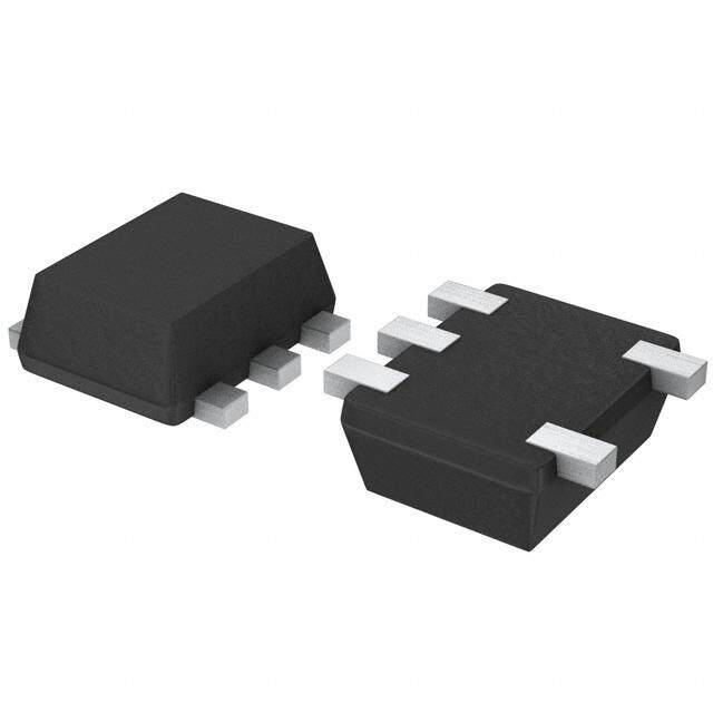
| 封装/外壳 | TO-226-3、TO-92-3 标准主体 |
| 封装/箱体 | TO-92-3 |
| 工作温度 | -40°C ~ 125°C |
| 工作电源电流 | 20 uA |
| 工厂包装数量 | 1000 |
| 最大工作温度 | + 125 C |
| 最小工作温度 | - 40 C |
| 标准包装 | 1,000 |
| 欠电压阈值 | 2.285 V |
| 电压-阈值 | 2.32V |
| 电池备用开关 | No Backup |
| 电源电压-最大 | 5.5 V |
| 电源电压-最小 | 1 V |
| 监视器 | No Watchdog |
| 类型 | Voltage Supervisory |
| 系列 | MCP121 |
| 被监测输入数 | 1 Input |
| 输出 | 开路漏极或开路集电极 |
| 输出类型 | Active Low, Open Drain |
| 过电压阈值 | 2.355 V |
| 阈值电压 | 2.32 V |

,TO-226_straightlead.jpg)


PDF Datasheet 数据手册内容提取
MCP102/103/121/131 Micropower Voltage Supervisors Features Package Types • Ultra low supply current: 1.75µA SOT23-3/SC-70 TO-92 (steady-state max.) (cid:129) Precision monitoring options of: 1 RST 1 13 - 1.90V, 2.32V, 2.63V, 2.93V, 3.08V, 4.38V 1/ 2 and 4.63V 1 2/ 3 VSS RST (cid:129) Resets microcontroller in a power-loss event 10 VDDVSS (cid:129) RST pin (Active-low): P - MCP121: Active-low, open-drain VDD 2 MC - MCP131: Active-low, open-drain with internal pull-up resistor SOT23-3/SC-70 - MCP102 and MCP103: Active-low, push-pull (cid:129) Reset Delay Timer (120ms delay, typ.) VSS 1 (cid:129) Available in SOT23-3, TO-92 and SC-70 3 0 packages P1 3 VDD C (cid:129) Temperature Range: M - Extended: -40°C to +125°C RST 2 (except MCP1XX-195) - Industrial: -40°C to +85°C (MCP1XX-195 only) (cid:129) Pb-free devices Block Diagram Applications V DD (cid:129) Critical Microcontroller and Microprocessor R (1) Power-monitoring Applications Comparator (cid:129) Computers + (cid:129) Intelligent Instruments Reset Output Delay Driver (cid:129) Portable Battery-powered Equipment – Circuit RST General Description Band Gap The MCP102/103/121/131 are voltage supervisor Reference devices designed to keep a microcontroller in reset until the system voltage has reached and stabilized at the proper level for reliable system operation. Table1 V SS Note 1: MCP131 Only shows the available features for these devices. TABLE 1: DEVICE FEATURES Output Reset Package Pinout Device Comment Delay (typ) (Pin # 1, 2, 3) Type Pull-up Resistor MCP102 Push-pull No 120ms RST, V , V DD SS MCP103 Push-pull No 120ms VSS, RST, VDD MCP121 Open-drain External 120ms RST, V , V DD SS MCP131 Open-drain Internal (~95kΩ) 120ms RST, V , V DD SS MCP111 Open-drain External No V , V , V See MCP111/112 Data Sheet OUT SS DD (DS21889) MCP112 Push-Pull No No V , V , V See MCP111/112 Data Sheet OUT SS DD (DS21889) © 2005 Microchip Technology Inc. DS21906B-page 1
MCP102/103/121/131 1.0 ELECTRICAL † Notice: Stresses above those listed under “Maximum Ratings” may cause permanent damage to the device. This is CHARACTERISTICS a stress rating only and functional operation of the device at those or any other conditions above those indicated in the Absolute Maximum Ratings† operational listings of this specification is not implied. Exposure to maximum rating conditions for extended periods VDD . . . . . . . . . . . . . . . . . . . . . . . . . . . . . . . . . . . . . . . . . 7.0V may affect device reliability. Input current (V ) . . . . . . . . . . . . . . . . . . . . . . . . . . . .10mA DD Output current (RST) . . . . . . . . . . . . . . . . . . . . . . . . . .10mA Rated Rise Time of V . . . . . . . . . . . . . . . . . . . . . . 100V/µs DD All inputs and outputs (except RST) w.r.t. V SS . . . . . . . . . . . . . . . . . . . . . . . . . . . . . . .-0.6V to (V + 1.0V) DD RST output w.r.t. V . . . . . . . . . . . . . . . . . . . -0.6V to 13.5V SS Storage temperature. . . . . . . . . . . . . . . . . . -65°C to + 150°C Ambient temp. with power applied . . . . . . . -40°C to + 125°C Maximum Junction temp. with power applied. . . . . . . .150°C ESD protection on all pins. . . . . . . . . . . . . . . . . . . . . . . . . ≥ 2kV DC CHARACTERISTICS Electrical Specifications: Unless otherwise indicated, all limits are specified for: V = 1V to 5.5V, R = 100kΩ (MCP121 only), DD PU T = -40°C to +125°C. A Parameters Sym Min Typ Max Units Conditions Operating Voltage Range V 1.0 — 5.5 V DD Specified V Value to RST low V 1.0 — V I = 10uA, V < 0.2V DD DD RST RST Operating Current MCP102, I — < 1 1.75 µA Reset Power-up Timer (t ) Inactive DD RPU MCP103, MCP121 — — 20.0 µA Reset Power-up Timer (t ) Active RPU MCP131 I — < 1 1.75 µA V > V and Reset Power-up DD DD TRIP Timer (t ) Inactive RPU — — 75 µA V < V and Reset Power-up DD TRIP Timer (t ) Inactive (Note3) RPU — — 90 µA Reset Power-up Timer (t ) Active RPU (Note4) Note 1: Trip point is ±1.5% from typical value. 2: Trip point is ±2.5% from typical value. 3: RST output is forced low. There is a current through the internal pull-up resistor. 4: This includes the current through the internal pull-up resistor and the reset power-up timer. 5: This specification allows this device to be used in PICmicro® microcontroller applications that require In-Circuit Serial Programming™ (ICSP™) (see device-specific programming specifications for voltage requirements). This specification DOES NOT allow a continuos high voltage to be present on the open-drain output pin (V ). The total time that the OUT V pin can be above the maximum device operational voltage (5.5V) is 100s. Current into the V pin should be OUT OUT limited to 2mA and it is recommended that the device operational temperature be maintained between 0°C to 70°C (+25°C preferred). For additional information, please refer to Figure2-33. 6: This parameter is established by characterization and not 100% tested. DS21906B-page 2 © 2005 Microchip Technology Inc.
MCP102/103/121/131 DC CHARACTERISTICS (CONTINUED) Electrical Specifications: Unless otherwise indicated, all limits are specified for: V = 1V to 5.5V, R = 100kΩ (MCP121 only), DD PU T = -40°C to +125°C. A Parameters Sym Min Typ Max Units Conditions V Trip Point MCP1XX-195 V 1.872 1.900 1.929 V T = +25°C (Note1) DD TRIP A 1.853 1.900 1.948 V T = -40°C to +85°C (Note2) A MCP1XX-240 2.285 2.320 2.355 V T = +25°C (Note1) A 2.262 2.320 2.378 V Note2 MCP1XX-270 2.591 2.630 2.670 V T = +25°C (Note1) A 2.564 2.630 2.696 V Note2 MCP1XX-300 2.886 2.930 2.974 V T = +25°C (Note1) A 2.857 2.930 3.003 V Note2 MCP1XX-315 3.034 3.080 3.126 V T = +25°C (Note1) A 3.003 3.080 3.157 V Note2 MCP1XX-450 4.314 4.380 4.446 V T = +25°C (Note1) A 4.271 4.380 4.490 V Note2 MCP1XX-475 4.561 4.630 4.700 V T = +25°C (Note1) A 4.514 4.630 4.746 V Note2 V Trip Point Tempco T — ±100 — ppm/°C DD TPCO Threshold MCP1XX-195 V 0.019 — 0.114 V T = +25°C HYS A Hysteresis MCP1XX-240 0.023 — 0.139 V (min. = 1%, max = 6%) MCP1XX-270 0.026 — 0.158 V MCP1XX-300 0.029 — 0.176 V MCP1XX-315 0.031 — 0.185 V MCP1XX-450 0.044 — 0.263 V MCP1XX-475 0.046 — 0.278 V RST Low-level Output Voltage V — — 0.4 V I = 500µA, V = V OL OL DD TRIP(MIN) RST High-level Output Voltage V V – 0.6 — — V I = 1mA, For MCP102/MCP103 OH DD OH (MCP102 and MCP103 only) only (push-pull output) Internal Pull-up Resistor R — 95 — kΩ V = 5.5V PU DD (MCP131 only) Open-drain High Voltage on Output V — — 13.5 (5) V V = 3.0V, Time voltage > 5.5V ODH DD (MCP121 only) applied ≤ 100s, current into pin limited to 2mA, 25°C operation recommended (Note5, Note6) Open-drain Output Leakage Current I — 0.1 — µA OD (MCP121 only) Note 1: Trip point is ±1.5% from typical value. 2: Trip point is ±2.5% from typical value. 3: RST output is forced low. There is a current through the internal pull-up resistor. 4: This includes the current through the internal pull-up resistor and the reset power-up timer. 5: This specification allows this device to be used in PICmicro® microcontroller applications that require In-Circuit Serial Programming™ (ICSP™) (see device-specific programming specifications for voltage requirements). This specification DOES NOT allow a continuos high voltage to be present on the open-drain output pin (V ). The total time that the OUT V pin can be above the maximum device operational voltage (5.5V) is 100s. Current into the V pin should be OUT OUT limited to 2mA and it is recommended that the device operational temperature be maintained between 0°C to 70°C (+25°C preferred). For additional information, please refer to Figure2-33. 6: This parameter is established by characterization and not 100% tested. © 2005 Microchip Technology Inc. DS21906B-page 3
MCP102/103/121/131 V TRIP 1V VDD tRPU t RPD V OH 1V V RST OL t RT FIGURE 1-1: Timing Diagram. AC CHARACTERISTICS Electrical Specifications: Unless otherwise indicated, all limits are specified for: V = 1V to 5.5V, R = 100kΩ (MCP121 only), DD PU T = -40°C to +125°C. A Parameters Sym Min Typ Max Units Conditions V Detect to RST Inactive t 80 120 180 ms Figure1-1 and C = 50pF DD RPU L V Detect to RST Active t — 130 — µs V ramped from V + DD RPD DD TRIP(MAX) 250mV down to V – TRIP(MIN) 250mV, per Figure1-1, C = 50pF (Note1) L RST Rise Time After RSTActive t — 5 — µs For RST 10% to 90% of final value RT (MCP102 and MCP103 only) per Figure1-1, C = 50pF L (Note1) Note 1: These parameters are for design guidance only and are not 100% tested. TEMPERATURE CHARACTERISTICS Electrical Specifications: Unless otherwise noted, all limits are specified for: V = 1V to 5.5V, R = 100kΩ (MCP121 only), DD PU T = -40°C to +125°C. A Parameters Sym Min Typ Max Units Conditions Temperature Ranges Specified Temperature Range T -40 — +85 ºC MCP1XX-195 A Specified Temperature Range T -40 — +125 ºC Except MCP1XX-195 A Maximum Junction Temperature T — — +150 ºC J Storage Temperature Range T -65 — +150 ºC A Package Thermal Resistances Thermal Resistance, 3L-SOT23 θ — 336 — ºC/W JA Thermal Resistance, 3L-SC-70 θ — 340 — ºC/W JA Thermal Resistance, 3L-TO-92 θ — 131.9 — ºC/W JA DS21906B-page 4 © 2005 Microchip Technology Inc.
MCP102/103/121/131 2.0 TYPICAL PERFORMANCE CURVES Note: The graphs and tables provided following this note are a statistical summary based on a limited number of samples and are provided for informational purposes only. The performance characteristics listed herein are not tested or guaranteed. In some graphs or tables, the data presented may be outside the specified operating range (e.g., outside specified power supply range) and therefore outside the warranted range. Note: Unless otherwise indicated, all limits are specified for: V = 1V to 5.5V, R = 100kΩ (MCP121 only; DD PU see Figure 4-1), T = -40°C to +125°C. A 1.8 16 1.6 MCP102-195 5.5V 14 MCP102-195 5.0V 1.4 12 5.5V A) 1.21 4.0V A) 10 5.0V I (uDD00..68 22..18VV I (uDD 68 4.0V 1.7V 0.4 4 2.8V 0.2 1.0V 2 2.1V 0 0 0 0 0 0 0 0 0 0 0 0 0 0 0 0 0 0 0 0 0 0 4 2 2 4 6 8 0 2 4 4 2 2 4 6 8 0 2 4 - - 1 1 1 - - 1 1 1 Temperature (°C) Temperature (°C) FIGURE 2-1: I vs. Temperature FIGURE 2-4: I vs. Temperature DD DD (Reset Power-up Timer Inactive) (MCP102-195). (Reset Power-up Timer Active) (MCP102-195). 35 80 MCP131-315 2.9V MCP131-315 30 70 25 60 5.5V 5.0V A) 20 A) 50 4.5V I (uDD15 I (uDD3400 34..30VV 10 20 1.0V 5 3.3V, 4.0V, 5.0V, 5.5V 10 0 0 0 0 0 0 0 0 0 0 0 0 0 0 0 0 0 0 0 0 0 0 4 2 2 4 6 8 0 2 4 4 2 2 4 6 8 0 2 4 - - 1 1 1 - - 1 1 1 Temperature (°C) Temperature (°C) FIGURE 2-2: I vs. Temperature FIGURE 2-5: I vs. Temperature DD DD (Reset Power-up Timer Inactive) (MCP131-315). (Reset Power-up Timer Active) (MCP131-315). 0.9 16 0.8 MCP121-450 5.5V 14 MCP121-450 0.7 12 5.5V 0.6 5.0V (uA)D00..45 4.8V (uA)D180 454...608VVV ID00..23 4.1V 4.6V 3.0V ID 46 0.1 1.0V 2 0 0 0 0 0 0 0 0 0 0 0 0 0 0 0 0 0 0 0 0 0 0 4 2 2 4 6 8 0 2 4 4 2 2 4 6 8 0 2 4 - - 1 1 1 - - 1 1 1 Temperature (°C) Temperature (°C) FIGURE 2-3: I vs. Temperature FIGURE 2-6: I vs. Temperature DD DD (Reset Power-up Timer Inactive) (MCP121-450). (Reset Power-up Timer Active) (MCP121-450). © 2005 Microchip Technology Inc. DS21906B-page 5
MCP102/103/121/131 Note: Unless otherwise indicated, all limits are specified for: V = 1V to 5.5V, R = 100kΩ (MCP121 only; DD PU see Figure 4-1), T = -40°C to +125°C. A 1.8 16 MCP102-195 MCP102-195 -40°C 0°C 1.6 14 +25°C 1.4 +25°C 12 +70°C +125°C +85°C I (uA)DD 001...6821 +85°C 0°C I (uA)DD1680 DtDtRReePPvUvU iiiiccnneeaa cciinnttii vvRReeeesseett +125°C 0.4 -40°C 4 0.2 2 0 0 1.0 2.0 3.0 4.0 5.0 6.0 1.0 2.0 3.0 4.0 5.0 6.0 VDD (V) VDD (V) FIGURE 2-7: I vs. V FIGURE 2-10: I vs.V DD DD DD DD (Reset Power-up Timer Inactive) (MCP102-195). (Reset Power-up Timer Active) (MCP102-195). 35 80 MCP131-315 0°C, +25°C MCP131-315 -40°C, 0°C +25°C 30 -40°C 70 +70°C 25 60 +85°C Device in Reset +125°C A) 20 +70° A) 50 tRPU inactive I (uDD 1105 +85°CC I (uDD 3400 5 +125°C 20 0 10 -5 0 1.0 2.0 3.0 4.0 5.0 6.0 1.0 2.0 3.0 4.0 5.0 6.0 VDD (V) VDD (V) FIGURE 2-8: I vs. V FIGURE 2-11: I vs.V DD DD DD DD (Reset Power-up Timer Inactive) (MCP131-315). (Reset Power-up Timer Active) (MCP131-315). 0.9 16 MCP121-450 MCP121-450 -40°C 0.8 14 0°C +25°C 0.7 12 +70°C 0.6 +125°C +70°C 10 Device in Reset +85°C uA) 0.5 uA) 8 tRPU inactive +125°C (DD0.4 +85°C (DD 6 I 0.3 I 4 0.2 0°C 2 -40°C 0.1 +25°C 0 0 -2 1.0 2.0 3.0 4.0 5.0 6.0 1.0 2.0 3.0 4.0 5.0 6.0 V (V) V (V) DD DD FIGURE 2-9: I vs. V FIGURE 2-12: I vs.V DD DD DD DD (Reset Power-up Timer Inactive) (MCP121-450). (Reset Power-up Timer Active) (MCP121-450). DS21906B-page 6 © 2005 Microchip Technology Inc.
MCP102/103/121/131 Note: Unless otherwise indicated, all limits are specified for: V = 1V to 5.5V, R = 100kΩ (MCP121; DD PU see Figure 4-1), T = -40°C to +125°C. A 0.120 1.945 0.050 MCP102-195 1.940 VTRIP, increasing VDD 0.045 0.100 VDD = 1.7V +70°C 11..993305 VHYS, Hysteresis 00..003450 0.080 +125°C V (V)TRIP111...999122505 000...000223050 Hyst (V) V (V)OL 00..004600 +85°C +25°C 1.910 0.015 0.020 0°C -40°C 1.905 VTRIP, decreasing VDD 0.010 0.000 1.900 0.005 MCP102-195 1.895 0.000 -0.020 -60 -10 40 90 140 0.00 0.25 0.50 0.75 1.00 Temperature (°C) IOL (mA) FIGURE 2-13: V vs. Temperature vs. FIGURE 2-16: V vs. I TRIP OL OL Hysteresis (MCP102-195). (MCP102-195 @ V = 1.7V). DD 0.070 3.200 0.108 MCP131-315 3.180 VTRIP, increasing VDD 0.106 0.060 VDD = 2.9V +70°C 0.104 0.050 +125°C V (V)TRIP 3333....111102460000 VTRIP, decreVaHsYSin, gH yVsDtDeresis 00000.....000119990046802 Hyst (V) V (V)OL 000...000234000 +85°C 0°C -40°C 3.080 0.092 0.010 +25°C MCP131-315 3.060 0.090 0.000 -60 -10 40 90 140 0.00 0.25 0.50 0.75 1.00 Temperature (°C) IOL (mA) FIGURE 2-14: V vs. Temperature vs. FIGURE 2-17: V vs. I TRIP OL OL Hysteresis (MCP131-315). (MCP131-315 @ V = 2.9V). DD 4.550 0.190 0.060 MCP121-450 0.180 0.050 VDD = 4.1V +85°C 4.500 VTRIP, increasing VDD 0.170 +125°C V (V)TRIP 44..440500 VTRIP, deVcHrYeSa, sHiynsgt eVrDeDsis 0000....111134560000 Hyst (V) V (V)OL000...000234000 +70°C +25°C 4.350 0.120 0.010 0°C 0.110 MCP121-450 -40°C 4.300 0.100 0.000 -60 -20 20 60 100 140 0.00 0.25 0.50 0.75 1.00 Temperature (°C) IOL (mA) FIGURE 2-15: V vs. Temperature vs. FIGURE 2-18: V vs. I TRIP OL OL Hysteresis (MCP121-450). (MCP121-450 @ V = 4.1V). DD © 2005 Microchip Technology Inc. DS21906B-page 7
MCP102/103/121/131 Note: Unless otherwise indicated, all limits are specified for: V = 1V to 5.5V, R = 100kΩ (MCP121 only; DD PU see Figure 4-1), T = -40°C to +125°C. A 0.140 2.110 MCP102-195 MCP102-195 0.120 VDD = 1.7 V IOL = 1.00 mA 2.090 VDD = 2.1V 0.100 2.070 V) 0.080 IOL = 0.75 mA V) 2.050 0°C -40°C V (OL0.060 IOL = 0.50 mA V (OH22..001300 +125°C 0.040 IOL = 0.25 mA 1.990 +85°C +70°C 0.020 1.970 +25°C IOL = 0.00 mA 0.000 1.950 -40 0 40 80 120 0.00 0.25 0.50 0.75 1.00 Temperature (°C) IOL (mA) FIGURE 2-19: V vs. Temperature FIGURE 2-22: V vs. I OL OH OL (MCP102-195 @ V = 1.7V). (MCP102-195 @ V = 2.1V). DD DD 0.070 IOL = 1.00 mA MCP131-315 0.060 VDD = 2.9V 0.050 IOL = 0.75 mA V (V)OL00..003400 IOL = 0.50 mA 0.020 IOL = 0.25 mA 0.010 IOL = 0.00 mA 0.000 -40 0 40 80 120 Temperature (°C) FIGURE 2-20: V vs. Temperature OL (MCP131-315 @ V = 2.9V). DD 0.060 MCP121-450 0.050 VDD = 4.1V IOL = 1.00 mA 0.040 IOL = 0.75 mA V) (OL0.030 IOL = 0.50 mA V 0.020 IOL = 0.25 mA 0.010 IOL = 0.00 mA 0.000 -40 0 40 80 120 Temperature (°C) FIGURE 2-21: V vs. Temperature OL (MCP121-450 @ V = 4.1V). DD DS21906B-page 8 © 2005 Microchip Technology Inc.
MCP102/103/121/131 Note: Unless otherwise indicated, all limits are specified for: V = 1V to 5.5V, R = 100kΩ (MCP121 only; DD PU see Figure 4-1), T = -40°C to +125°C. A 300 160 VDD decreasing MCP102-195 MCP102-195 from: 5V - 1.7V 250 150 VDD decreasing from: VDD increasing from: 200 VTRIP(max) + 0.25V to VTRIP(min) - 0.25V 140 0V - 2.1V µs) µs) V0VDD - i2n.c8rVeasing from: t (RPD 110500 t (RPU 112300 VDD increasing from: 0V - 4.0V 50 110 VDD decreasing VDD increasing from: 5V - 0V from: 0V - 5.5V 0 100 -40 -15 10 35 60 85 110 -40 -15 10 35 60 85 110 Temperature (°C) Temperature (°C) FIGURE 2-23: t vs. Temperature FIGURE 2-26: t vs. Temperature RPD RPU (MCP102-195). (MCP102-195). 250 160 VDD decreasing from: MCP131-315 VDD increasing from: MCP131-315 VTRIP(max) + 0.25V to VTRIP(min) - 0.25V 150 0V - 3.3V 200 VDD increasing from: 0V - 4.0V 140 t (µs)RPD 110500 V5VDD - d0eVcreasing from: V5VDD - d2e.7cVreasing from: t (µs)RPU112300 VDD increasing from: 50 0V - 4.5V 110 VDD increasing from: 0V - 5.5V 0 100 -40 -15 10 35 60 85 110 -40 -15 10 35 60 85 110 Temperature (°C) Temperature (°C) FIGURE 2-24: t vs. Temperature FIGURE 2-27: t vs. Temperature RPD RPU (MCP131-315). (MCP131-315). 38 145 MCP121-450 MCP121-450 37.5 VDD increasing from: 140 VDD increasing from: t (µs)RT 363.57 0V - 4.6V V0VDD - i4n.c8rVeasing from: (µs)RPU 111233505 0V - 4.8V 36 t 120 VDD increasing from: 0V - 5.0V 35.5 VDD increasing from: VDD increasing from: 115 VDD increasing from: 0V - 5.0V 0V - 5.5V 0V - 5.5V 35 110 -40 -15 10 35 60 85 110 -40 -15 10 35 60 85 110 Temperature (°C) Temperature (°C) FIGURE 2-25: t vs. Temperature FIGURE 2-28: t vs. Temperature RPD RPU (MCP121-450). (MCP121-450). © 2005 Microchip Technology Inc. DS21906B-page 9
MCP102/103/121/131 Note: Unless otherwise indicated, all limits are specified for: V = 1V to 5.5V, R = 100kΩ (MCP121 only; DD PU see Figure 4-1), T = -40°C to +125°C. A 0.45 1400 0.4 V0VDD - i2n.c1rVeasing from: MCP102-195 S) 1200 MCP121-450 µ t (µs)RT 0000000....0123...5152535 V0VDD - i5n.c5rVeasing from: VDD increV0V0aVVDDsDD i-- n ii24nng..cc80 frrVVreeoaamssii:nngg ffrroomm:: Transient Duration ( 1246800000000000 MMCCPP110321--139155 0V - 5.0V 0 0 -40 -15 10 35 60 85 110 0.001 0.01 0.1 1 10 Temperature (°C) VTRIP(Min) - VDD FIGURE 2-29: t vs. Temperature FIGURE 2-32: Transient Duration vs. RT (MCP102-195). V (min) - V . TRIP DD 45 101.0m0E-02 4413 VDD incV0rVeDaD - s i5nin.c5grVe farosmin:g from: V0VDD - i5n.c0rVeasing from: ge (A)110111100...000m000µµEEE---000543 39 0V - 4.5V ka 1.100Eµ-06 t (µs)RT 333357 Drain Lea110111100...000000nnnEEE---000987 +125°C 31 n-1010.00pE-10 +25°C 29 V0VDD - i3n.c3rVeasing from: Ope 110.00pE-11 - 40°C 2257 V0VDD - i4n.c0rVeasing from: MCP131-315 10111..00000pEEf--1132 -40 -15 10 35 60 85 110 0 1 2 3 4 5 6 7 8 9 10 11 12 13 14 Temperature (°C) Pull-Up Voltage (V) FIGURE 2-30: t vs. Temperature FIGURE 2-33: Open-Drain Leakage RT (MCP131-315). Current vs. Voltage Applied to V Pin OUT (MCP121-195). 38 MCP121-450 37.5 VDD increasing from: 37 0V - 4.6V V0VDD - i4n.c8rVeasing from: s) µ (RT 36.5 t 36 35.5 VDD increasing from: VDD increasing from: 0V - 5.0V 0V - 5.5V 35 -40 -15 10 35 60 85 110 Temperature (°C) FIGURE 2-31: t vs. Temperature RT (MCP121-450). DS21906B-page 10 © 2005 Microchip Technology Inc.
MCP102/103/121/131 3.0 PIN DESCRIPTION The descriptions of the pins are listed in Table3-1. TABLE 3-1: PIN FUNCTION TABLE Pin No. MCP102 Symbol Function MCP121 MCP103 MCP131 1 1 RST Output State V Falling: DD H = V > V DD TRIP L = V < V DD TRIP V Rising: DD H = V > V + V DD TRIP HYS L = V < V + V DD TRIP HYS 2 3 V Positive power supply DD 3 2 V Ground reference SS © 2005 Microchip Technology Inc. DS21906B-page 11
MCP102/103/121/131 4.0 APPLICATION INFORMATION 4.1 RST Operation For many of today’s microcontroller applications, care The RST output pin operation determines how the must be taken to prevent low-power conditions that can device can be used and indicates when the system cause many different system problems. The most should be forced into reset. To accomplish this, an common causes are brown-out conditions, where the internal voltage reference is used to set the voltage trip system supply drops below the operating level momen- point (VTRIP). Additionally, there is a hysteresis on this tarily. The second most common cause is when a trip point. slowly decaying power supply causes the When the falling edge of V crosses this voltage DD microcontroller to begin executing instructions without threshold, the reset power-down timer (T ) starts. RPD sufficient voltage to sustain volitile memory (RAM), thus When this delay timer times out, the RST pin is forced producing indeterminate results. Figure4-1 shows a low. typical application circuit. When the rising-edge of V crosses this voltage DD The MCP102/103/121/131 are voltage supervisor threshold, the reset power-up timer (T ) starts. RPU devices designed to keep a microcontroller in reset When this delay timer times out, the RST pin is forced until the system voltage has reached and stabilized at high, T is active and there is additional system RPU the proper level for reliable system operation. These current. devices also operate as protection from brown-out The actual voltage trip point (V ) will be between conditions. TRIPAC the minimum trip point (V ) and the maximum TRIPMIN trip point (V ). The hysteresis on this trip point V TRIPMAX DD and the delay timer (T ) are to remove any “jitter” RPU VDD that would occur on the RST pin when the device VDD V is at the trip point. 0.1 DD R PICmicro® MCP1XX PU Microcontroller Figure4-2 shows the waveform of the RST pin as deter- µF mined by the V voltage, while Table4-1 shows the MCLR DD RST (Reset input) state of the RST pin. The VTRIP specification is for falling (Active-low) VDD voltages. When the VDD voltage is rising, the RST VSS V will not be driven high until VDD is at VTRIP + VHYS. Once SS V has crossed the voltage trip point, there is also a DD minimal delay time (T ) before the RST pin is driven RPD low. Note1: Resistor R may be required with the PU TABLE 4-1: RST PIN STATES MCP121 due to the open-drain output. Resistor RPU may not be required with State of RST Pin when: the MCP131 due to the internal pull-up Device V < V V > Ouput Driver resistor. The MCP102 and MCP103 do DD TRIP DD not require the external pull-up resistor. VTRIP + VHYS MCP102 L H Push-pull FIGURE 4-1: Typical Application Circuit. MCP103 L H Push-pull MCP121 L H (1) Open-drain (1) MCP131 L H (2) Open-drain (2) Note1: Requires External Pull-up resistor 2: Has Internal Pull-up resistor V DD V + V V TRIPAC HYSAC TRIPMAX V TRIPAC VTRIPMIN VTRIPAC 1V RST t RPU t < 1V is outside the RPU t tRPD device specifications RPD FIGURE 4-2: RST Operation as Determined by the V and V . TRIP HYS DS21906B-page 12 © 2005 Microchip Technology Inc.
MCP102/103/121/131 4.2 Negative Going V Transients 4.3 Reset Power-up Timer (t ) DD RPU The minimum pulse width (time) required to cause a Figure4-4 illustrates the device current states. While reset may be an important criteria in the implementa- the system is powering down, the device has a low tion of a Power-on Reset (POR) circuit. This time is current. This current is dependent on the device V DD referred to as transient duration, defined as the amount and trip point. When the device V rises through the DD of time needed for these supervisory devices to voltage trip point (V ), an internal timer starts. This TRIP respond to a drop in V . The transient duration time is timer consumes additional current until the RST pin is DD dependant on the magnitude of V – V . Generally driven (or released) high. This time is known as the TRIP DD speaking, the transient duration decreases with Reset Power-up Time (t ). Figure4-4 shows when RPU increases in V – V . t is active (device consuming additional current). TRIP DD RPU Figure4-3 shows a typical transient duration vs. reset comparator overdrive, for which the V DD MCP102/103/121/131 will not generate a reset pulse. It shows that the farther below the trip point the transient V TRIP pulse goes, the duration of the pulse required to cause a reset gets shorter. Figure2-32 shows the transient response characteristics for the MCP102/103/121/131. A 0.1µF bypass capacitor, mounted as close as RST possible to the VDD pin, provides additional transient tRPU immunity (refer to Figure4-1). 5eV VVTRIP(MAX) er-upe g TRIP(MIN) wv ply Volta VTRIP(MIN) - VDD Reset Power-up eset Pomer Acti RPTioemwseeertr-up up tTRANS Timer Inactive RTi Inactive S 0V Time (µs) See Figures2-1, See Figures2-1, FIGURE 4-3: Example of Typical 2-2 and2-3 2-2 and2-3 Transient Duration Waveform. See Figures2-4, 2-5 and 2-6 FIGURE 4-4: Reset Power-up Timer Waveform. 4.3.1 EFFECT OF TEMPERATURE ON RESET POWER-UP TIMER (T ) RPU The Reset Power-up timer time-out period (t ) RPU determines how long the device remains in the reset condition. This is affected by both V and temperature. DD Typical responses for different V values and DD temperatures are shown in Figures2-26,2-27 and2-28. © 2005 Microchip Technology Inc. DS21906B-page 13
MCP102/103/121/131 4.4 Using in PICmicro® Microcontroller, ICSP™ Applications (MCP121 only) Figure4-5 shows the typical application circuit for using the MCP121 for voltage superviory function when the PICmicro microcontroller will be programmed via the ICSP feature. Additional information is available in TB087, “Using Voltage Supervisors with PICmicro® Microcontroller Systems which Implement In-Circuit Serial Programming™”, DS91087. Note: It is recommended that the current into the RST pin be current limited by a 1kΩ resistor. V /V DD PP 0.1µF V DD VDD RPU PICmicro® MCP121 MCU MCLR RST (Reset Input) 1kΩ (Active-low) V SS V SS FIGURE 4-5: Typical Application Circuit for PICmicro® Microcontroller with the ICSP™ feature. DS21906B-page 14 © 2005 Microchip Technology Inc.
MCP102/103/121/131 5.0 PACKAGING INFORMATION 5.1 Package Marking Information 3-Lead TO-92 Example: XXXXXX MCP102 XXXXXX 195I XXXXXX TO^e^3 YWWNNN 547256 Example: MCP1xx = 3-Pin SOT-23 Part Number MCP102 MCP103 MCP121 MCP131 MCP1xxT-195I/TT JGNN TGNN LGNN KGNN MCP1xxT-240ETT JHNN THNN LHNN KHNN XXNN MCP1xxT-270E/TT JJNN TJNN LJNN KJNN MCP1xxT-300E/TT JKNN TKNN LKNN KKNN MCP1xxT-315E/TT JLNN TLNN LLNN KLNN MCP1xxT-450E/TT JMNN TMNN LMNN KMNN MCP1xxT-475E/TT JPNN TPNN LPNN KPNN Legend: XX...X Customer-specific information Y Year code (last digit of calendar year) WW Week code (week of January 1 is week ‘01’) NNN Alphanumeric traceability code e3 Pb-free JEDEC designator for Matte Tin (Sn) * This package is Pb-free. The Pb-free JEDEC designator ( e 3 ) can be found on the outer packaging for this package. Note: In the event the full Microchip part number cannot be marked on one line, it will be carried over to the next line, thus limiting the number of available characters for customer-specific information. © 2005 Microchip Technology Inc. DS21906B-page 15
MCP102/103/121/131 Package Marking Information (Continued) Example: MCP1xx = 3-Pin SC-70 Part Number MCP102 MCP103 MCP121 MCP131 MCP1xxT-195I/LB BGN FGN DGN CGN MCP1xxT-240E/LB BHN FHN DHN CHN XXN YWW MCP1xxT-270E/LB BJN FJN DJN CJN MCP1xxT-300E/LB BKN FKN DKN CKN MCP1xxT-315E/LB BLN FLN DLN CLN Top Side Bottom Side MCP1xxT-450E/LB BMN FMN DMN CMN MCP1xxT-475E/LB BPN FPN DPN CPN OR Example: MCP1xx = Part Number MCP102 MCP103 MCP121 MCP131 MCP1xxT-195I/LB BGNN FGNN DGNN CGNN MCP1xxT-240E/LB BHNN FHNN DHNN CHNN XXNN MCP1xxT-270E/LB BJNN FJNN DJNN CJNN MCP1xxT-300E/LB BKNN FKNN DKNN CKNN MCP1xxT-315E/LB BLNN FLNN DLNN CLNN Top Side MCP1xxT-450E/LB BMNN FMNN DMNN CMNN MCP1xxT-475E/LB BPNN FPNN DPNN CPNN DS21906B-page 16 © 2005 Microchip Technology Inc.
MCP102/103/121/131 3-Lead Plastic Small Outline Transistor (TT) (SOT-23) E E1 2 B p1 D n p 1 α c A A2 φ A1 β L Units INCHES* MILLIMETERS Dimension Limits MIN NOM MAX MIN NOM MAX Number of Pins n 3 3 Pitch p .038 0.96 Outside lead pitch (basic) p1 .076 1.92 Overall Height A .035 .040 .044 0.89 1.01 1.12 Molded Package Thickness A2 .035 .037 .040 0.88 0.95 1.02 Standoff § A1 .000 .002 .004 0.01 0.06 0.10 Overall Width E .083 .093 .104 2.10 2.37 2.64 Molded Package Width E1 .047 .051 .055 1.20 1.30 1.40 Overall Length D .110 .115 .120 2.80 2.92 3.04 Foot Length L .014 .018 .022 0.35 0.45 0.55 Foot Angle φ 0 5 10 0 5 10 Lead Thickness c .004 .006 .007 0.09 0.14 0.18 Lead Width B .015 .017 .020 0.37 0.44 0.51 Mold Draft Angle Top α 0 5 10 0 5 10 Mold Draft Angle Bottom β 0 5 10 0 5 10 * Controlling Parameter § Significant Characteristic Notes: Dimensions D and E1 do not include mold flash or protrusions. Mold flash or protrusions shall not exceed .010” (0.254mm) per side. JEDEC Equivalent: TO-236 Drawing No. C04-104 © 2005 Microchip Technology Inc. DS21906B-page 17
MCP102/103/121/131 3-Lead Plastic Small Outline Transistor (LB) (SC-70) E E1 B 2 p1 D 3 p 1 a c A A2 b L A1 Units INCHES MILLIMETERS* Dimension Limits MIN MAX MIN MAX Number of Pins 3 3 Pitch p .026 BSC. 0.65 BSC. Outside lead pitch (basic) p1 .051 BSC. 1.30 BSC. Overall Height A .031 .043 0.80 1.10 Molded Package Thickness A2 .031 .039 0.80 1.00 Standoff A1 .000 .0004 0.00 .010 Overall Width E .071 .094 1.80 2.40 Molded Package Width E1 .045 .053 1.15 1.35 Overall Length D .071 .089 1.80 2.25 Foot Length L .004 .016 0.10 0.41 Lead Thickness c .003 .010 0.08 0.25 Lead Width B .006 .016 0.15 0.40 Mold Draft Angle Top a 8° 12° 8° 12° Mold Draft Angle Bottom b 8° 12° 8° 12° *Controlling Parameter Notes: Dimensions D and E1 do not include mold flash or protrusions. Mold flash or protrusions shall not exceed .005" (0.127mm) per side. JEITA (EIAJ) Equivalent: SC70 Drawing No. C04-104 DS21906B-page 18 © 2005 Microchip Technology Inc.
MCP102/103/121/131 3-Lead Plastic Transistor Outline (TO) (TO-92) E1 D 1 n L 1 2 3 α B p c A R β Units INCHES* MILLIMETERS Dimension Limits MIN NOM MAX MIN NOM MAX Number of Pins n 3 3 Pitch p .050 1.27 Bottom to Package Flat A .130 .143 .155 3.30 3.62 3.94 Overall Width E1 .175 .186 .195 4.45 4.71 4.95 Overall Length D .170 .183 .195 4.32 4.64 4.95 Molded Package Radius R .085 .090 .095 2.16 2.29 2.41 Tip to Seating Plane L .500 .555 .610 12.70 14.10 15.49 Lead Thickness c .014 .017 .020 0.36 0.43 0.51 Lead Width B .016 .019 .022 0.41 0.48 0.56 Mold Draft Angle Top α 4 5 6 4 5 6 Mold Draft Angle Bottom β 2 3 4 2 3 4 *Controlling Parameter Notes: Dimensions D and E1 do not include mold flash or protrusions. Mold flash or protrusions shall not exceed .010” (0.254mm) per side. JEDEC Equivalent: TO-92 Drawing No. C04-101 © 2005 Microchip Technology Inc. DS21906B-page 19
MCP102/103/121/131 5.2 Product Tape and Reel Specifications FIGURE 5-1: EMBOSSED CARRIER DIMENSIONS (8, 12, 16 AND 24 MM TAPE ONLY) Top Cover Tape A 0 W K0 B0 P TABLE 1: CARRIER TAPE/CAVITY DIMENSIONS Carrier Cavity Dimensions Dimensions Output Reel Case Package Quantity Diameter in Outline Type W P A0 B0 K0 Units mm mm mm mm mm mm TT SOT-23 3L 8 4 3.15 2.77 1.22 3000 180 LB SC-70 3L 8 4 2.4 2.4 1.19 3000 180 FIGURE 5-2: 3-LEAD SOT-23/SC70 DEVICE TAPE AND REEL SPECIFICATIONS User Direction of Feed Device Marking W PIN 1 P Standard Reel Component Orientation DS21906B-page 20 © 2005 Microchip Technology Inc.
MCP102/103/121/131 FIGURE 5-3: TO-92 DEVICE TAPE AND REEL SPECIFICATIONS User Direction of Feed P Device Marking MARK MARK MARK FACE FACE FACE Seal Tape Back W Tape Note: Bent leads are for Tape and Reel only. © 2005 Microchip Technology Inc. DS21906B-page 21
MCP102/103/121/131 NOTES: DS21906B-page 22 © 2005 Microchip Technology Inc.
MCP102/103/121/131 APPENDIX A: REVISION HISTORY Revision B (March 2005) The following is the list of modifications: 1. Added Section4.4 “Using in PICmicro® Microcontroller, ICSP™ Applications (MCP121 only)” on using the MCP121 in PICmicro microcontroller ICSP applications. 2. Added V specifications in Section1.0 ODH “Electrical Characteristics” (for ICSP applications). 3. Added Figure 2-33. 4. Updated SC-70 package markings and added Pb-free marking information to Section5.0 “Packaging information”. 5. Added Appendix A: “Revision History”. Revision A (August 2004) (cid:129) Original Release of this Document. © 2005 Microchip Technology Inc. DS21906B-page 23
MCP102/103/121/131 NOTES: DS21906B-page 24 © 2005 Microchip Technology Inc.
MCP102/103/121/131 PRODUCT IDENTIFICATION SYSTEM To order or obtain information, e.g., on pricing or delivery, refer to the factory or the listed sales office. PART NO. – X XXX X / XX Examples: a) MCP102T-195I/TT: Tape and Reel, Device Tape/Reel Monitoring Temperature Package 1.95V MicroPower Option Options Range Voltage Supervisor, push-pull, -40°C to +85°C, SOT-23B-3 package. b) MCP102-300E/TO: 3.00V MicroPower Device: MCP102: MicroPower Voltage Supervisor, push-pull MCP102T:MicroPower Voltage Supervisor, push-pull Voltage Supervisor, (Tape and Reel) push-pull, -40°C to +125°C, MCP103: MicroPower Voltage Supervisor, push-pull MCP103T:MicroPower Voltage Supervisor, push-pull TO-92-3 package. (Tape and Reel) a) MCP103T-270E/TT:Tape and Reel, MCP121 MicroPower Voltage Supervisor, open-drain 2.70V MicroPower MCP121T:MicroPower Voltage Supervisor, open-drain Voltage Supervisor, (Tape and Reel) push-pull, MCP131 MicroPower Voltage Supervisor, open-drain -40°C to +125°C, MCP131T:MicroPower Voltage Supervisor, open-drain SOT-23B-3 package. (Tape and Reel) b) MCP103T-475E/LB:Tape and Reel, 4.75V MicroPower Monitoring Options: 195 = 1.90V Voltage Supervisor, 240 = 2.32V push-pull, 270 = 2.63V -40°C to +125°C, 300 = 2.93V SC-70-3 package. 315 = 3.08V a) MCP121T-315I/LB: Tape and Reel, 450 = 4.38V 3.15V MicroPower 475 = 4.63V Voltage Supervisor, open-drain, -40°C to +125°C, Temperature Range: I = -40°C to +85°C (MCP11X-195 only) SC-70-3 package. E = -40°C to +125°C (Except MCP11X-195 only) b) MCP121-300E/TO: 3.00V MicroPower Voltage Supervisor, Package: TT = SOT-23B, 3-lead open-drain, LB = SC-70, 3-lead -40°C to +125°C, TO = TO-92, 3-lead TO-92-3 package. a) MCP131T-195I/TT: Tape and Reel, 1.95V MicroPower Voltage Supervisor, open-drain, -40°C to +85°C, SOT-23B-3 package. b) MCP131-300E/TO: 3.00V MicroPower Voltage Supervisor, open-drain, -40°C to +125°C, TO-92-3 package. © 2005 Microchip Technology Inc. DS21906B-page 25
MCP102/103/121/131 NOTES: DS21906B-page 26 © 2005 Microchip Technology Inc.
Note the following details of the code protection feature on Microchip devices: (cid:129) Microchip products meet the specification contained in their particular Microchip Data Sheet. (cid:129) Microchip believes that its family of products is one of the most secure families of its kind on the market today, when used in the intended manner and under normal conditions. (cid:129) There are dishonest and possibly illegal methods used to breach the code protection feature. All of these methods, to our knowledge, require using the Microchip products in a manner outside the operating specifications contained in Microchip’s Data Sheets. Most likely, the person doing so is engaged in theft of intellectual property. (cid:129) Microchip is willing to work with the customer who is concerned about the integrity of their code. (cid:129) Neither Microchip nor any other semiconductor manufacturer can guarantee the security of their code. Code protection does not mean that we are guaranteeing the product as “unbreakable.” Code protection is constantly evolving. We at Microchip are committed to continuously improving the code protection features of our products. Attempts to break Microchip’s code protection feature may be a violation of the Digital Millennium Copyright Act. If such acts allow unauthorized access to your software or other copyrighted work, you may have a right to sue for relief under that Act. Information contained in this publication regarding device Trademarks applications and the like is provided only for your convenience The Microchip name and logo, the Microchip logo, Accuron, and may be superseded by updates. It is your responsibility to dsPIC, KEELOQ, microID, MPLAB, PIC, PICmicro, PICSTART, ensure that your application meets with your specifications. PROMATE, PowerSmart, rfPIC, and SmartShunt are MICROCHIP MAKES NO REPRESENTATIONS OR WAR- registered trademarks of Microchip Technology Incorporated RANTIES OF ANY KIND WHETHER EXPRESS OR IMPLIED, in the U.S.A. and other countries. WRITTEN OR ORAL, STATUTORY OR OTHERWISE, RELATED TO THE INFORMATION, INCLUDING BUT NOT AmpLab, FilterLab, Migratable Memory, MXDEV, MXLAB, LIMITED TO ITS CONDITION, QUALITY, PERFORMANCE, PICMASTER, SEEVAL, SmartSensor and The Embedded MERCHANTABILITY OR FITNESS FOR PURPOSE. Control Solutions Company are registered trademarks of Microchip disclaims all liability arising from this information and Microchip Technology Incorporated in the U.S.A. its use. Use of Microchip’s products as critical components in Analog-for-the-Digital Age, Application Maestro, dsPICDEM, life support systems is not authorized except with express dsPICDEM.net, dsPICworks, ECAN, ECONOMONITOR, written approval by Microchip. No licenses are conveyed, FanSense, FlexROM, fuzzyLAB, In-Circuit Serial implicitly or otherwise, under any Microchip intellectual property Programming, ICSP, ICEPIC, MPASM, MPLIB, MPLINK, rights. MPSIM, PICkit, PICDEM, PICDEM.net, PICLAB, PICtail, PowerCal, PowerInfo, PowerMate, PowerTool, rfLAB, rfPICDEM, Select Mode, Smart Serial, SmartTel, Total Endurance and WiperLock are trademarks of Microchip Technology Incorporated in the U.S.A. and other countries. SQTP is a service mark of Microchip Technology Incorporated in the U.S.A. All other trademarks mentioned herein are property of their respective companies. © 2005, Microchip Technology Incorporated, Printed in the U.S.A., All Rights Reserved. Printed on recycled paper. Microchip received ISO/TS-16949:2002 quality system certification for its worldwide headquarters, design and wafer fabrication facilities in Chandler and Tempe, Arizona and Mountain View, California in October 2003. The Company’s quality system processes and procedures are for its PICmicro® 8-bit MCUs, KEELOQ® code hopping devices, Serial EEPROMs, microperipherals, nonvolatile memory and analog products. In addition, Microchip’s quality system for the design and manufacture of development systems is ISO 9001:2000 certified. © 2005 Microchip Technology Inc. DS21906B-page 27
WORLDWIDE SALES AND SERVICE AMERICAS ASIA/PACIFIC ASIA/PACIFIC EUROPE Corporate Office Australia - Sydney India - Bangalore Austria - Weis 2355 West Chandler Blvd. Tel: 61-2-9868-6733 Tel: 91-80-2229-0061 Tel: 43-7242-2244-399 Chandler, AZ 85224-6199 Fax: 61-2-9868-6755 Fax: 91-80-2229-0062 Fax: 43-7242-2244-393 Tel: 480-792-7200 China - Beijing India - New Delhi Denmark - Ballerup Fax: 480-792-7277 Tel: 86-10-8528-2100 Tel: 91-11-5160-8631 Tel: 45-4450-2828 Technical Support: Fax: 86-10-8528-2104 Fax: 91-11-5160-8632 Fax: 45-4485-2829 http://support.microchip.com Web Address: China - Chengdu Japan - Kanagawa France - Massy www.microchip.com Tel: 86-28-8676-6200 Tel: 81-45-471- 6166 Tel: 33-1-69-53-63-20 Fax: 86-28-8676-6599 Fax: 81-45-471-6122 Fax: 33-1-69-30-90-79 Atlanta Alpharetta, GA China - Fuzhou Korea - Seoul Germany - Ismaning Tel: 770-640-0034 Tel: 86-591-8750-3506 Tel: 82-2-554-7200 Tel: 49-89-627-144-0 Fax: 770-640-0307 Fax: 86-591-8750-3521 Fax: 82-2-558-5932 or Fax: 49-89-627-144-44 China - Hong Kong SAR 82-2-558-5934 Italy - Milan Boston Westborough, MA Tel: 852-2401-1200 Singapore Tel: 39-0331-742611 Tel: 774-760-0087 Fax: 852-2401-3431 Tel: 65-6334-8870 Fax: 39-0331-466781 Fax: 774-760-0088 China - Shanghai Fax: 65-6334-8850 Netherlands - Drunen Chicago Tel: 86-21-5407-5533 Taiwan - Kaohsiung Tel: 31-416-690399 Itasca, IL Fax: 86-21-5407-5066 Tel: 886-7-536-4818 Fax: 31-416-690340 Tel: 630-285-0071 China - Shenyang Fax: 886-7-536-4803 England - Berkshire Fax: 630-285-0075 Tel: 86-24-2334-2829 Taiwan - Taipei Tel: 44-118-921-5869 Dallas Fax: 86-24-2334-2393 Tel: 886-2-2500-6610 Fax: 44-118-921-5820 Addison, TX China - Shenzhen Fax: 886-2-2508-0102 Tel: 972-818-7423 Tel: 86-755-8203-2660 Taiwan - Hsinchu Fax: 972-818-2924 Fax: 86-755-8203-1760 Tel: 886-3-572-9526 Detroit China - Shunde Fax: 886-3-572-6459 Farmington Hills, MI Tel: 86-757-2839-5507 Tel: 248-538-2250 Fax: 86-757-2839-5571 Fax: 248-538-2260 China - Qingdao Kokomo Tel: 86-532-502-7355 Kokomo, IN Fax: 86-532-502-7205 Tel: 765-864-8360 Fax: 765-864-8387 Los Angeles Mission Viejo, CA Tel: 949-462-9523 Fax: 949-462-9608 San Jose Mountain View, CA Tel: 650-215-1444 Fax: 650-961-0286 Toronto Mississauga, Ontario, Canada Tel: 905-673-0699 Fax: 905-673-6509 03/01/05 DS21906B-page 28 © 2005 Microchip Technology Inc.
Mouser Electronics Authorized Distributor Click to View Pricing, Inventory, Delivery & Lifecycle Information: M icrochip: MCP102-195I/TO MCP103T-195I/TT MCP103T-195I/LB MCP102T-315E/TT MCP102-270E/TO MCP121T-450E/TT MCP121T-450E/LB MCP131-240E/TO MCP102T-240E/TT MCP102-450E/TO MCP121-315E/TO MCP131T- 450E/LB MCP102-240E/TO MCP121-475E/TO MCP131-315E/TO MCP103T-300E/LB MCP131T-475E/LB MCP131T-475E/TT MCP121-270E/TO MCP103T-270E/LB MCP103T-270E/TT MCP121-450E/TO MCP103T- 450E/TT MCP103T-450E/LB MCP102-300E/TO MCP131T-270E/LB MCP131T-270E/TT MCP102-315E/TO MCP131T-195I/TT MCP131T-195I/LB MCP102T-300E/TT MCP121T-475E/LB MCP121T-475E/TT MCP131- 300E/TO MCP121T-195I/TT MCP131T-315E/LB MCP131T-315E/TT MCP102T-450E/LB MCP102T-450E/TT MCP131-450E/TO MCP121-300E/TO MCP103T-300E/TT MCP102-475E/TO MCP131T-240E/LB MCP121T- 270E/TT MCP121T-270E/LB MCP121T-315E/LB MCP121T-315E/TT MCP102T-195I/LB MCP102T-195I/TT MCP102T-240E/LB MCP121T-240E/TT MCP121T-240E/LB MCP103T-475E/LB MCP103T-475E/TT MCP103T- 315E/TT MCP103T-315E/LB MCP103T-240E/LB MCP103T-240E/TT MCP121-240E/TO MCP131-270E/TO MCP102T-270E/LB MCP121T-300E/TT MCP121T-300E/LB MCP121-195I/TO MCP131-195I/TO MCP102T-475E/TT MCP102T-475E/LB MCP131-475E/TO MCP131T-300E/TT MCP131T-300E/LB