ICGOO在线商城 > 集成电路(IC) > PMIC - 监控器 > STM6503VEAADG6F
 Datasheet下载
- 型号: STM6503VEAADG6F
- 制造商: STMicroelectronics
- 库位|库存: xxxx|xxxx
- 要求:
| 数量阶梯 | 香港交货 | 国内含税 |
| +xxxx | $xxxx | ¥xxxx |
查看当月历史价格
查看今年历史价格
STM6503VEAADG6F产品简介:
ICGOO电子元器件商城为您提供STM6503VEAADG6F由STMicroelectronics设计生产,在icgoo商城现货销售,并且可以通过原厂、代理商等渠道进行代购。 STM6503VEAADG6F价格参考。STMicroelectronicsSTM6503VEAADG6F封装/规格:PMIC - 监控器, 开路漏极或开路集电极 监控器 1 通道 8-TDFN(2x2)。您可以下载STM6503VEAADG6F参考资料、Datasheet数据手册功能说明书,资料中有STM6503VEAADG6F 详细功能的应用电路图电压和使用方法及教程。
STM6503VEAADG6F 是 STMicroelectronics(意法半导体)推出的一款 PMIC(电源管理集成电路),属于 PMIC - 监控器类别。该型号主要应用于需要高效电源管理和系统监控的场景,以下是其典型应用场景:

1. 工业自动化设备
   STM6503VEAADG6F 可用于工业控制器、PLC(可编程逻辑控制器)和数据采集系统中,提供稳定的电源管理和实时监控功能,确保设备在复杂环境下可靠运行。

2. 通信基础设施
   在基站、路由器和交换机等通信设备中,该芯片可用于管理多路电源输出,并监控电压、电流和温度等关键参数,以保障系统的稳定性和安全性。

3. 嵌入式计算系统
   适用于单板计算机(SBC)、工业级主板和其他嵌入式计算平台,为处理器、存储器和外设提供精确的电源分配和保护机制。

4. 医疗设备
   在便携式医疗设备(如监护仪、血糖仪)或大型医疗成像设备中,该 PMIC 能够优化功耗并确保电源的高精度和低噪声,满足医疗应用的严格要求。

5. 汽车电子系统
   用于车载信息娱乐系统、ADAS(高级驾驶辅助系统)和车身控制模块中,提供高效的电源转换和全面的系统保护功能,适应汽车环境的严苛条件。

6. 消费类电子产品
   在高端智能手机、平板电脑和智能音箱等产品中,该芯片能够实现动态电源调整和电池状态监控,延长设备续航时间并提升用户体验。

总之,STM6503VEAADG6F 凭借其高性能、灵活性和可靠性,广泛适用于对电源管理和系统监控有较高要求的各种领域,特别是在工业、通信、医疗和汽车等行业中发挥重要作用。
| 参数 | 数值 |
| 产品目录 | 集成电路 (IC)半导体 |
| 描述 | IC DUAL SMART RESET 8TDFN开关 IC - 各种 Smart push-button Dual-Assert Reset |
| 产品分类 | |
| 品牌 | STMicroelectronics |
| 产品手册 | |
| 产品图片 |
|
| rohs | 符合RoHS无铅 / 符合限制有害物质指令(RoHS)规范要求 |
| 产品系列 | 开关 IC,开关 IC - 各种,STMicroelectronics STM6503VEAADG6FSmart Reset™ |
| 数据手册 | |
| 产品型号 | STM6503VEAADG6F |
| 产品培训模块 | http://www.digikey.cn/PTM/IndividualPTM.page?site=cn&lang=zhs&ptm=24998 |
| 产品目录页面 | |
| 产品种类 | 开关 IC - 各种 |
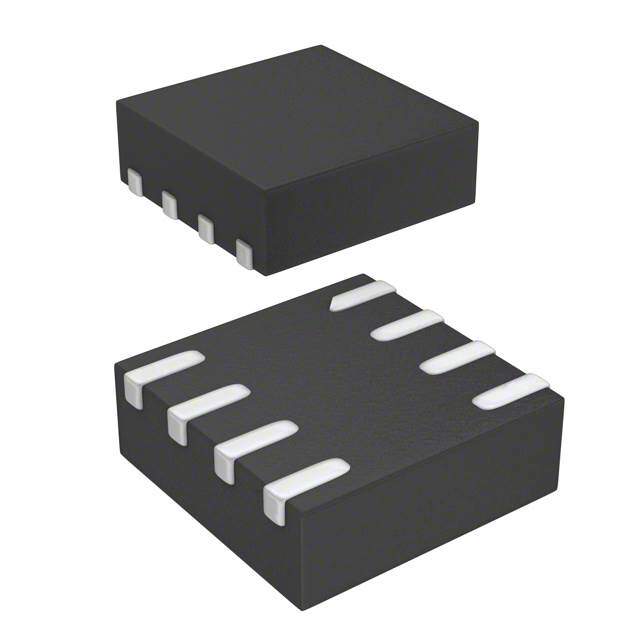
| 供应商器件封装 | 8-TDFN(2x2) |
| 其它名称 | 497-10053-1 |
| 其它有关文件 | http://www.st.com/web/catalog/sense_power/FM1946/SC1296/PF219501?referrer=70071840 |
| 包装 | 剪切带 (CT) |
| 受监控电压数 | 1 |
| 商标 | STMicroelectronics |
| 复位 | 低有效 |
| 复位超时 | 最小为 140 ms |
| 安装类型 | 表面贴装 |
| 安装风格 | SMD/SMT |
| 封装 | Reel |
| 封装/外壳 | 8-WFDFN 裸露焊盘 |
| 封装/箱体 | TDFN-8 |
| 工作温度 | -40°C ~ 85°C |
| 工厂包装数量 | 3000 |
| 开关数量 | Dual |
| 最大工作温度 | + 85 C |
| 最小工作温度 | - 40 C |
| 标准包装 | 1 |
| 特色产品 | http://www.digikey.com/cn/zh/ph/st/stm65x.html |
| 电压-阈值 | 1.575V |
| 电源电压-最大 | 5.5 V |
| 电源电压-最小 | 1 V |
| 电源电流 | 4 uA |
| 类型 | 重置计时器 |
| 系列 | STM6503 |
| 输出 | 开路漏极或开路集电极 |


- 商务部:美国ITC正式对集成电路等产品启动337调查
- 曝三星4nm工艺存在良率问题 高通将骁龙8 Gen1或转产台积电
- 太阳诱电将投资9.5亿元在常州建新厂生产MLCC 预计2023年完工
- 英特尔发布欧洲新工厂建设计划 深化IDM 2.0 战略
- 台积电先进制程称霸业界 有大客户加持明年业绩稳了
- 达到5530亿美元!SIA预计今年全球半导体销售额将创下新高
- 英特尔拟将自动驾驶子公司Mobileye上市 估值或超500亿美元
- 三星加码芯片和SET,合并消费电子和移动部门,撤换高东真等 CEO
- 三星电子宣布重大人事变动 还合并消费电子和移动部门
- 海关总署:前11个月进口集成电路产品价值2.52万亿元 增长14.8%


PDF Datasheet 数据手册内容提取
STM6502, STM6503 STM6504, STM6505 TM Dual push-button Smart Reset with user-adjustable setup delays Features ■ Dual Smart Reset push-button inputs with extended reset setup delay ■ Adjustable Smart Reset setup delay (t ): SRC by external capacitor or three-state logic (product options): t = 2, 6, 10 s (min.) SRC ■ Power-on reset TDFN8 (DG) ■ Single RST output, active-low, open-drain 2 mm x 2 mm ■ Factory-programmable thresholds to monitor V in the range of 1.575 to 4.625 V typ. CC Applications ■ Operating voltage 1.0 V (active-low output valid) to 5.5 V ■ Mobile phones, smartphones ■ Low supply current ■ e-books ■ Operating temperature: ■ MP3 players industrial grade –40 °C to +85 °C ■ Games ■ Portable navigation devices ■ TDFN8 package: 2 mm x 2 mm x 0.75 mm ■ Any application that requires delayed reset ■ RoHS compliant push-button(s) response for improved system stability Table 1. Device summary t Reset or Power Voltage inputs Smart Reset inputs SRC programming Good outputs Part Three- Package number SRE Ext. state V V SR0 SR1 immediate, RST BLD CC BAT SRC pin input independent TSR STM6502(1) ✓ ✓ ✓ ✓ ✓ TDFN-8L STM6503 ✓ ✓ ✓ ✓ ✓ TDFN-8L STM6504(1) ✓ ✓ ✓ ✓ ✓ TDFN-8L STM6505 ✓ ✓ ✓ ✓ ✓ ✓ ✓ TDFN-8L 1. Contact local ST sales office for availability. February 2011 Doc ID 16101 Rev 6 1/29 www.st.com 1
Contents STM6502, STM6503, STM6504, STM6505 Contents 1 Description . . . . . . . . . . . . . . . . . . . . . . . . . . . . . . . . . . . . . . . . . . . . . . . . . 5 1.1 Smart Reset devices . . . . . . . . . . . . . . . . . . . . . . . . . . . . . . . . . . . . . . . . . 5 1.2 Pin descriptions . . . . . . . . . . . . . . . . . . . . . . . . . . . . . . . . . . . . . . . . . . . . 10 1.2.1 Power supply (V ) . . . . . . . . . . . . . . . . . . . . . . . . . . . . . . . . . . . . . . . . 10 CC 1.2.2 Ground (V ) . . . . . . . . . . . . . . . . . . . . . . . . . . . . . . . . . . . . . . . . . . . . . 10 SS 1.2.3 Primary Smart Reset input (SR0) . . . . . . . . . . . . . . . . . . . . . . . . . . . . . 10 1.2.4 Secondary Smart Reset input (SR1) . . . . . . . . . . . . . . . . . . . . . . . . . . . 10 1.2.5 Edge-triggered Smart Reset input (SRE pin) – STM6504 only . . . . . . . 11 1.2.6 Adjustable delay of Smart Reset input (SRC pin) – STM6502 and STM6505 only . . . . . . . . . . . . . . . . . . . . . . . . . . . . . . . . . . . . . . . . . 11 1.2.7 Programmable Smart Reset input delay (TSR pin) – STM6503 and STM6504 only . . . . . . . . . . . . . . . . . . . . . . . . . . . . . . . . . . . . . . . . . 12 1.2.8 Reset output (RST) . . . . . . . . . . . . . . . . . . . . . . . . . . . . . . . . . . . . . . . . 12 1.2.9 Battery monitoring input (V ) – STM6505 only . . . . . . . . . . . . . . . . . 12 BAT 1.2.10 Battery low detect output (BLD) – STM6505 only . . . . . . . . . . . . . . . . . 12 2 Typical operating characteristics . . . . . . . . . . . . . . . . . . . . . . . . . . . . . 13 3 Maximum ratings . . . . . . . . . . . . . . . . . . . . . . . . . . . . . . . . . . . . . . . . . . . 15 4 DC and AC parameters . . . . . . . . . . . . . . . . . . . . . . . . . . . . . . . . . . . . . . 16 5 Package mechanical data . . . . . . . . . . . . . . . . . . . . . . . . . . . . . . . . . . . . 20 6 Part numbering . . . . . . . . . . . . . . . . . . . . . . . . . . . . . . . . . . . . . . . . . . . . 26 7 Package marking . . . . . . . . . . . . . . . . . . . . . . . . . . . . . . . . . . . . . . . . . . . 27 8 Revision history . . . . . . . . . . . . . . . . . . . . . . . . . . . . . . . . . . . . . . . . . . . 28 2/29 Doc ID 16101 Rev 6
STM6502, STM6503, STM6504, STM6505 List of tables List of tables Table 1. Device summary. . . . . . . . . . . . . . . . . . . . . . . . . . . . . . . . . . . . . . . . . . . . . . . . . . . . . . . . . . 1 Table 2. Signal names . . . . . . . . . . . . . . . . . . . . . . . . . . . . . . . . . . . . . . . . . . . . . . . . . . . . . . . . . . . . 7 Table 3. t programmed by an ideal external capacitor – STM6502 and STM6505 . . . . . . . . . . 11 SRC Table 4. Absolute maximum ratings. . . . . . . . . . . . . . . . . . . . . . . . . . . . . . . . . . . . . . . . . . . . . . . . . 15 Table 5. Operating and measurement conditions. . . . . . . . . . . . . . . . . . . . . . . . . . . . . . . . . . . . . . . 16 Table 6. DC and AC characteristics . . . . . . . . . . . . . . . . . . . . . . . . . . . . . . . . . . . . . . . . . . . . . . . . . 17 Table 7. V voltage thresholds. . . . . . . . . . . . . . . . . . . . . . . . . . . . . . . . . . . . . . . . . . . . . . . . . . . . 19 CC Table 8. TDFN – 8-lead 2 x 2 x 0.75 mm, 0.5 mm pitch package mechanical data. . . . . . . . . . . . . 21 Table 9. Parameter for landing pattern - TDFN – 8-lead 2 x 2 mm package . . . . . . . . . . . . . . . . . . 22 Table 10. Carrier tape dimensions . . . . . . . . . . . . . . . . . . . . . . . . . . . . . . . . . . . . . . . . . . . . . . . . . . . 23 Table 11. Reel dimensions. . . . . . . . . . . . . . . . . . . . . . . . . . . . . . . . . . . . . . . . . . . . . . . . . . . . . . . . . 24 Table 12. Ordering information scheme. . . . . . . . . . . . . . . . . . . . . . . . . . . . . . . . . . . . . . . . . . . . . . . 26 Table 13. Package marking . . . . . . . . . . . . . . . . . . . . . . . . . . . . . . . . . . . . . . . . . . . . . . . . . . . . . . . . 27 Table 14. Document revision history . . . . . . . . . . . . . . . . . . . . . . . . . . . . . . . . . . . . . . . . . . . . . . . . . 28 Doc ID 16101 Rev 6 3/29
STM6502, STM6503, STM6504, STM6505 List of figures List of figures Figure 1. Logic diagrams. . . . . . . . . . . . . . . . . . . . . . . . . . . . . . . . . . . . . . . . . . . . . . . . . . . . . . . . . . . 6 Figure 2. Pin connections . . . . . . . . . . . . . . . . . . . . . . . . . . . . . . . . . . . . . . . . . . . . . . . . . . . . . . . . . . 6 Figure 3. Block diagram - STM6502, STM6503, STM6504. . . . . . . . . . . . . . . . . . . . . . . . . . . . . . . . . 8 Figure 4. Block diagram - STM6505 . . . . . . . . . . . . . . . . . . . . . . . . . . . . . . . . . . . . . . . . . . . . . . . . . . 8 Figure 5. Single-button Smart Reset typical hookup . . . . . . . . . . . . . . . . . . . . . . . . . . . . . . . . . . . . . . 9 Figure 6. Dual-button Smart Reset typical hookup . . . . . . . . . . . . . . . . . . . . . . . . . . . . . . . . . . . . . . . 9 Figure 7. STM6502, STM6503 timing . . . . . . . . . . . . . . . . . . . . . . . . . . . . . . . . . . . . . . . . . . . . . . . . 10 Figure 8. STM6504 timing . . . . . . . . . . . . . . . . . . . . . . . . . . . . . . . . . . . . . . . . . . . . . . . . . . . . . . . . . 11 Figure 9. STM6505 timing . . . . . . . . . . . . . . . . . . . . . . . . . . . . . . . . . . . . . . . . . . . . . . . . . . . . . . . . . 12 Figure 10. Supply current (I ) vs. temperature (STM6505). . . . . . . . . . . . . . . . . . . . . . . . . . . . . . . . 13 CC Figure 11. Smart Reset delay (t ) vs. temperature, C = 0.62 µF (STM6505) . . . . . . . . . . . . . . 13 SRC SRC Figure 12. Reset threshold (V ) vs. temperature, “S” threshold option, V falling (STM6505) . . . 14 RST CC Figure 13. V monitoring threshold (V )vs. temperature, falling (STM6505). . . . . . . . . . . . . . 14 BAT BATTH Figure 14. AC testing input/output waveforms. . . . . . . . . . . . . . . . . . . . . . . . . . . . . . . . . . . . . . . . . . . 16 Figure 15. TDFN – 8-lead 2 x 2 x 0.75 mm, 0.5 mm pitch package outline. . . . . . . . . . . . . . . . . . . . . 21 Figure 16. Landing pattern - TDFN – 8-lead 2 x 2 mm without thermal pad . . . . . . . . . . . . . . . . . . . . 22 Figure 17. Carrier tape . . . . . . . . . . . . . . . . . . . . . . . . . . . . . . . . . . . . . . . . . . . . . . . . . . . . . . . . . . . . 23 Figure 18. Reel dimensions. . . . . . . . . . . . . . . . . . . . . . . . . . . . . . . . . . . . . . . . . . . . . . . . . . . . . . . . . 24 Figure 19. Tape trailer/leader. . . . . . . . . . . . . . . . . . . . . . . . . . . . . . . . . . . . . . . . . . . . . . . . . . . . . . . . 25 Figure 20. Pin 1 orientation . . . . . . . . . . . . . . . . . . . . . . . . . . . . . . . . . . . . . . . . . . . . . . . . . . . . . . . . . 25 Figure 21. Package marking, top view. . . . . . . . . . . . . . . . . . . . . . . . . . . . . . . . . . . . . . . . . . . . . . . . . 27 Doc ID 16101 Rev 6 4/29
STM6502, STM6503, STM6504, STM6505 Description 1 Description STM6502 has two combined Smart Reset inputs (SR0 and SR1) with delayed Smart Reset setup time (t ) programmed by an external capacitor on the SRC pin. SRC STM6503 is similar to STM6502, has two combined delayed Smart Reset inputs (SR0, SR1) and three user-selectable delayed Smart Reset setup time (t ) options of 2 s, 6 s and 10 SRC s through a three-state TSR input pin: when connected to ground, t = 2 s; when left SRC open, t = 6 s; when connected to V , t = 10 s (all the times are minimum). SRC CC SRC STM6504 has two independent Smart Reset inputs. SR0 provides the delayed Smart Reset setup time (t ) function with three user-selectable t options through a three-state TSR SRC SRC input pin: when connected to ground, t = 2 s; when left open, t = 6 s; when SRC SRC connected to V , t = 10 s (all the times are minimum). SRE provides instant reset. SRE CC SRC is edge-triggered with a special debounce time (t = 240 ms min.) at the falling DEBOUNCE edge after a valid reset period. STM6505 has two combined delayed Smart Reset inputs (SR0, SR1) and provides an adjustable reset delay setup time via an external capacitor connected to the SRC pin. The RST output depends also on the V monitoring threshold. STM6505 also provides CC independent low battery detect (BLD) output controlled by the secondary external input voltage V . V is monitored for low voltage and provides an indication on the battery low BAT BAT detect output pin (BLD). V threshold is 1.25 V, fixed, and an external resistor divider is to BAT be used to set the actual battery voltage threshold. V threshold hysteresis is 8 mV typ. BAT (16 mV max.). V is voltage monitoring input only, the device is powered only from the BAT V pin; V must be ≥ 1.575 V for proper operation of the V comparator. CC CC BAT 1.1 Smart Reset devices The Smart Reset device family STM65xx provides a useful feature that ensures inadvertent short reset push-button closures do not cause system resets. This is done by implementing extended Smart Reset input delay (t ). Once the valid Smart Reset input levels and setup SRC delay are met, the device generates an output reset pulse with user-programmable timeout period (t ). REC The Smart Reset inputs can be also connected to the applications interrupt to allow the control of both the interrupt pin and the hard reset functions. If the push-buttons are closed for a short time, the processor is only interrupted. If the system still does not respond properly, holding the push-buttons for the extended setup time (t ) causes hard reset of SRC the processor through the reset outputs. The Smart Reset feature helps significantly increase system stability. The STM65xx family of Smart Reset devices consists of low current microprocessor reset circuits targeted at applications such as MP3 players, navigation, smartphones or mobile phones; generally any application that requires delayed reset push-button(s) response for improved system stability. The STM65xx devices feature single or dual Smart Reset inputs (SR). The delayed Smart Reset setup time (t ) options of 2 s, 6 s and 10 s (all min.) are SRC adjustable by an external capacitor on the SRC pin or selectable by three-state logic. The delayed setup period ignores switch closures shorter than t , thus preventing unwanted SRC resets. Doc ID 16101 Rev 6 5/29
Description STM6502, STM6503, STM6504, STM6505 The STM65xx devices have active-low (optionally active-high) open-drain reset (RST) output(s) with or without internal pull-up resistor or push-pull as output options, with factory- programmed or capacitor-adjustable or push-buttons defined output reset pulse duration, with or without power-on reset function. Some devices also have an undervoltage monitoring feature: the reset output is also asserted when the monitored supply voltage V drops below the specified threshold. The CC reset output remains asserted for the reset timeout period (t ) after the monitored supply REC voltage goes above the specified threshold. Figure 1. Logic diagrams VCC VCC SR0 SR0 SR1 STM6502 RST SR1 STM6503 RST TSR SRC VSS VSS VCC VCC SR0 SR0 SR1 RST SRE STM6504 RST STM6505 SRC BLD TSR VBAT VSS VSS AM00378 Figure 2. Pin connections RST 1 8 VCC RST 1 8 VCC VSS 2 STM 7 SR0 VSS 2 STM 7 SR0 6502 6503 SR1 3 6 SRC SR1 3 6 TSR NC 4 5 NC NC 4 5 NC RST 1 8 VCC RST 1 8 VCC VSS 2 STM 7 SR0 VSS 2 STM 7 SR0 6504 6505 SRE 3 6 TSR SR1 3 6 SRC NC 4 5 NC BLD 4 5 VBAT AM00379 6/29 Doc ID 16101 Rev 6
STM6502, STM6503, STM6504, STM6505 Description T able 2. Signal names Input/ Symbol Description output RST Output Open-drain reset output, active-low. BLD Output Battery low detect output, active-low, open-drain. STM6505 only. Primary push-button Smart Reset input. Active-low, with or without internal SR0 Input 65 kΩ pull-up to V (product options). CC Secondary push-button Smart Reset input - combines with the primary push- SR1 Input button reset to provide setup delay time before reset. Active-low, with or without internal 65 kΩ pull-up to V (product options). CC Secondary push-button Smart Reset input - provides instant Smart Reset. SRE is edge-triggered with a special debounce time (t = 240 ms min.) at SRE Input DEBOUNCE the falling edge after a valid reset period. Active-high, no internal pull-up to V . CC STM6504 only. Smart Reset input delay setup control: connect to an external capacitor to adjust SRC Input the delay setup time (t ). STM6502 and STM6505 only. SRC A three-state Smart Reset input delay setup control. When connected to ground, t = 2 s; when left open, t = 6 s; when connected to V , SRC SRC CC t = 10 s (all times are minimum). TSR is a DC-type input, intended to be SRC TSR Input either permanently grounded, permanently connected to V or permanently CC left open. If left open, for improved system glitch immunity it is strongly recommended to connect a 0.1 µF decoupling ceramic capacitor between the TSR and V pins. STM6503 and STM6504 only. SS Supply voltage input. Power supply for the device and an input for the monitored V Supply supply voltage. A 0.1 µF decoupling ceramic capacitor is recommended to be CC connected between the V and V pins. CC SS V Input Battery voltage monitoring input. STM6505 only. BAT V Supply Ground SS NC No connect (not bonded); should be connected to V . SS Doc ID 16101 Rev 6 7/29
Description STM6502, STM6503, STM6504, STM6505 Figure 3. Block diagram - STM6502, STM6503, STM6504 VCC VRST COMPARE SR1 (SRE Logic STM6504 only)(1) tREC RST generator SR0 Logic SRC (STM6502) TSR (STM6503, STM6504) AM00352a 1. STM6504 only: SR0 and SRE are working independently. SRE is edge-triggered and has a special debounce time (t = 240 ms min.) at the falling edge after a valid reset period. DEBOUNCE Figure 4. Block diagram - STM6505 (cid:54)(cid:34)(cid:33)(cid:52) (cid:54)(cid:34)(cid:33)(cid:52)(cid:52)(cid:40) (cid:35)(cid:47)(cid:45)(cid:48)(cid:33)(cid:50)(cid:37) (cid:34)(cid:44)(cid:36) (cid:54)(cid:35)(cid:35) (cid:54)(cid:50)(cid:51)(cid:52) (cid:35)(cid:47)(cid:45)(cid:48)(cid:33)(cid:50)(cid:37) (cid:54)(cid:35)(cid:35) (cid:84)(cid:50)(cid:37)(cid:35) (cid:50)(cid:51)(cid:52) (cid:71)(cid:69)(cid:78)(cid:69)(cid:82)(cid:65)(cid:84)(cid:79)(cid:82) (cid:51)(cid:50)(cid:16) (cid:44)(cid:79)(cid:71)(cid:73)(cid:67) (cid:51)(cid:50)(cid:17) (cid:51)(cid:50)(cid:35) (cid:33)(cid:45)(cid:16)(cid:16)(cid:19)(cid:17)(cid:25)(cid:66) 8/29 Doc ID 16101 Rev 6
STM6502, STM6503, STM6504, STM6505 Description Figure 5. Single-button Smart Reset typical hookup (cid:54)(cid:35)(cid:35) (cid:54)(cid:35)(cid:35) (cid:54)(cid:35)(cid:35) (cid:50)(cid:51)(cid:52) (cid:50)(cid:37)(cid:51)(cid:37)(cid:52) (cid:52)(cid:51)(cid:50) (cid:51)(cid:52)(cid:45)(cid:22)(cid:21)(cid:16)(cid:19) (cid:45)(cid:35)(cid:53) (cid:51)(cid:50)(cid:17) (cid:41)(cid:46)(cid:52)(cid:15) (cid:51)(cid:50)(cid:16) (cid:46)(cid:45)(cid:41) (cid:54)(cid:51)(cid:51) (cid:54)(cid:51)(cid:51) (cid:48)(cid:53)(cid:51)(cid:40)(cid:13)(cid:34)(cid:53)(cid:52)(cid:52)(cid:47)(cid:46) (cid:51)(cid:55)(cid:41)(cid:52)(cid:35)(cid:40) (cid:33)(cid:45)(cid:16)(cid:16)(cid:19)(cid:24)(cid:16)(cid:66) Figure 6. Dual-button Smart Reset typical hookup (cid:54)(cid:35)(cid:35) (cid:54)(cid:35)(cid:35) (cid:54)(cid:35)(cid:35) (cid:50)(cid:51)(cid:52) (cid:50)(cid:37)(cid:51)(cid:37)(cid:52) (cid:52)(cid:51)(cid:50) (cid:51)(cid:52)(cid:45)(cid:22)(cid:21)(cid:16)(cid:19) (cid:45)(cid:35)(cid:53) (cid:51)(cid:50)(cid:17) (cid:41)(cid:46)(cid:52)(cid:15) (cid:51)(cid:50)(cid:16) (cid:46)(cid:45)(cid:41) (cid:54)(cid:51)(cid:51) (cid:54)(cid:51)(cid:51) (cid:48)(cid:53)(cid:51)(cid:40)(cid:13)(cid:34)(cid:53)(cid:52)(cid:52)(cid:47)(cid:46) (cid:48)(cid:53)(cid:51)(cid:40)(cid:13)(cid:34)(cid:53)(cid:52)(cid:52)(cid:47)(cid:46) (cid:51)(cid:55)(cid:41)(cid:52)(cid:35)(cid:40) (cid:51)(cid:55)(cid:41)(cid:52)(cid:35)(cid:40) (cid:33)(cid:45)(cid:16)(cid:16)(cid:19)(cid:24)(cid:17)(cid:54)(cid:20) Doc ID 16101 Rev 6 9/29
Description STM6502, STM6503, STM6504, STM6505 1.2 Pin descriptions 1.2.1 Power supply (V ) CC This pin is used to provide the power to the device and to monitor the power supply. A 0.1 µF decoupling ceramic capacitor is recommended to be connected between the V CC and V pins. SS 1.2.2 Ground (V ) SS This is the supply ground for the device. 1.2.3 Primary Smart Reset input (SR0) The primary push-button Smart Reset input, active-low pin is connected to the first push- button switch. 1.2.4 Secondary Smart Reset input (SR1) The secondary push-button Smart Reset input, active-low pin is connected to the second push-button switch. Keeping both Smart Reset inputs SR0 and SR1 active for longer than t activates the reset output pulse. SRC Figure 7. STM6502, STM6503 timing tSRC tREC SR0 SR1 RST AM00327 Reset is asserted “low” right after the Smart Reset setup delay (t ) has been met and SRC returns to high after the t period. REC 10/29 Doc ID 16101 Rev 6
STM6502, STM6503, STM6504, STM6505 Description 1.2.5 Edge-triggered Smart Reset input (SRE pin) – STM6504 only The SRE pin is active-high, immediate and independent reset input that includes an edge trigger with debounce delay t on the falling edge. DEBOUNCE Note: The triggering edge must be a high-to-low or low-to-high transition with a slew-rate faster than 1 V/µs typ. Figure 8. STM6504 timing t < tDEBOUNCE t < tSRC => tREC timer reset => no output response tSRC SR0 Independent SRE No debounce RST tREC tDEBOUNCE tREC tREC (rising edges within tDEBOUNCE are ignored) AM00328V2 1.2.6 Adjustable delay of Smart Reset input (SRC pin) – STM6502 and STM6505 only This pin controls the setup time before the push-button action is validated by the reset output. It is connected to an external capacitor (C ), which is tied to ground to provide the SRC desired value of the setup time (t ). SRC Calculated t and C examples are given in Table3. Refer also to Table6. SRC SRC T able 3. t programmed by an ideal external capacitor – STM6502 and STM6505 SRC Setup delay t [s](1)(2) Calculated C SRC Closest common SRC value [µF] C value [µF] Min. Typ. Max. SRC 0.2 2 2.5 3.0 0.22 0.3 3 3.75 4.5 0.33 0.6 6 7.5 9 0.56 1 10 12.5 15 1 1. At 25 °C. Example calculations based on an ideal capacitor. During application design and component selection it should be considered that the current flowing into the external t programming capacitor SRC (C ) is on the order of 100 nA, therefore a low-leakage capacitor (ceramic or film capacitor) should be SRC used and placed as close as possible to the SRC pin. Also an adequate low-leakage PCB environment should be ensured to prevent t accuracy from being affected. A recommended minimum value of C SRC SRC is 0.01 µF. 2. In case of repeated activations of the t timer, an interval of 10 ms min. is needed between the SRC activations to fully discharge C , so that the next t is as specified. SRC SRC Doc ID 16101 Rev 6 11/29
Description STM6502, STM6503, STM6504, STM6505 1.2.7 Programmable Smart Reset input delay (TSR pin) – STM6503 and STM6504 only The TSR pin allows the user to program the setup time before the push-button action is validated by the reset output. It is controlled by different voltage levels on the three-state TSR input pin: when connected to ground, t = 2 s; when left open, t = 6 s; when SRC SRC connected to V , t = 10 s (all times are minimum). TSR is a DC-type input, intended to CC SRC be either permanently grounded, permanently connected to V or permanently left open. CC If it is left open, for improved system glitch immunity it is strongly recommended to connect a 0.1 µF decoupling ceramic capacitor between the TSR and V pins. SS 1.2.8 Reset output (RST) RST is the active-low, open-drain reset output in the Smart Reset family. 1.2.9 Battery monitoring input (V ) – STM6505 only BAT V is aninput for monitoring the battery voltage. V threshold is 1.25 V, fixed, and an BAT BAT external resistor divider is to be used to set the actual battery voltage threshold. 1.2.10 Battery low detect output (BLD) – STM6505 only The battery low detect output is controlled by the V voltage monitoring input and is BAT active-low, open-drain, with no pull-up. Figure 9. STM6505 timing tSRC tREC SR0 SR1 RST V BAT VBATTH BLD AM00329 12/29 Doc ID 16101 Rev 6
STM6502, STM6503, STM6504, STM6505 Typical operating characteristics 2 Typical operating characteristics Figure 10. Supply current (I ) vs. temperature (STM6505) CC 3 2.5 2 A] μ [C 1.5 C I 1 0.5 0 -60 -40 -20 0 20 40 60 80 100 120 140 Temperature [°C] 5.5 V 2 V 5 V 3 V AM04886v1 Figure 11. Smart Reset delay (t ) vs. temperature, C = 0.62 µF (STM6505) SRC SRC 9.2 8.7 8.2 s] [C 7.7 R S t 7.2 6.7 6.2 -60 -40 -20 0 20 40 60 80 100 120 140 Temperature [°C] 5.75 V 5.5 V 3.3 V AM04887v1 Doc ID 16101 Rev 6 13/29
Typical operating characteristics STM6502, STM6503, STM6504, STM6505 Figure 12. Reset threshold (V ) vs. temperature, “S” threshold option, V falling (STM6505) RST CC 2.99 2.97 2.95 V] 2.93 [T S R V 2.91 2.89 2.87 2.85 -60 -40 -20 0 20 40 60 80 100 120 140 Temperature [°C] AM04888v1 Figure 13. V monitoring threshold (V )vs. temperature, falling (STM6505) BAT BATTH 1.275 1.27 1.265 1.26 1.255 V] [H 1.25 T T A B V 1.245 1.24 1.235 1.23 1.225 -60 -40 -20 0 20 40 60 80 100 120 140 Temperature [°C] 5.75 V 5.5 V 3.3 V 2 V 1.58 V AM04889v1 14/29 Doc ID 16101 Rev 6
STM6502, STM6503, STM6504, STM6505 Maximum ratings 3 Maximum ratings Stressing the device above the rating listed in Table4: Absolute maximum ratings may cause permanent damage to the device. These are stress ratings only and operation of the device at these or any other conditions above those indicated in the operating sections of this specification is not implied. Exposure to absolute maximum rating conditions for extended periods may affect device reliability. Refer also to the STMicroelectronics SURE Program and other relevant quality documents. T able 4. Absolute maximum ratings Symbol Parameter Value Unit T Storage temperature (V off) –55 to +150 °C STG CC T (1) Lead solder temperature for 10 seconds 260 °C SLD θ Thermal resistance (junction to ambient) TDFN8 149.0 °C/W JA V Input or output voltage –0.3 to 5.5(2) V IO V Supply voltage –0.3 to 7 V CC 1. Reflow at peak temperature of 260 °C. The time above 255 °C must not exceed 30 seconds. 2. For inputs or outputs with internal pull-up resistors and push-pull type outputs –0.3 to V +0.3 V only. CC Doc ID 16101 Rev 6 15/29
DC and AC parameters STM6502, STM6503, STM6504, STM6505 4 DC and AC parameters This section summarizes the operating measurement conditions, and the DC and AC characteristics of the device. The parameters in the DC and AC characteristics tables that follow, are derived from tests performed under the measurement conditions summarized in Table5: Operating and measurement conditions. Designers should check that the operating conditions in their circuit match the operating conditions when relying on the quoted parameters. Table 5. Operating and measurement conditions Parameter Value Unit V supply voltage 1.0 to 5.5 V CC Ambient operating temperature (T ) –40 to +85 °C A Input rise and fall times ≤ 5 ns Input pulse voltages 0.2 to 0.8 V V CC Input and output timing ref. voltages 0.3 to 0.7 V V CC Figure 14. AC testing input/output waveforms 0.8 VCC 0.7 VCC 0.2 V 0.3 V CC CC AM00478 16/29 Doc ID 16101 Rev 6
STM6502, STM6503, STM6504, STM6505 DC and AC parameters Table 6. D C and AC characteristics Symbol Parameter Test conditions(1) Min. Typ.(2) Max. Unit V Supply voltage range Reset output valid - active-low 1.0 5.5 V CC V = 5.0 V 1.2 µA CC STM6502 V = 3.0 V(3) 1.1 µA CC V = 5.0 V, TSR left open 4 5.8 µA CC Supply current (inputs STM6503 V = 3.0 V, TSR left open(3) 3 µA in their inactive state, CC I CC t and t counter REC SRC V = 5.0 V, TSR left open 4 5.8 µA CC is inactive) STM6504 V = 3.0 V, TSR left open(3) 3 µA CC V = 5.0 V 2.3 3.3 µA CC STM6505 V = 3.0 V(3) 2.2 µA CC Output characteristics V ≥ 4.5 V, sinking 3.2 mA 0.3 V CC Reset output voltage low V V ≥ 3.3 V, sinking 2.5 mA 0.3 V OL (reset asserted: RST, BLD) CC V ≥ 1.0 V, sinking 0.1 mA 0.3 V CC Option A 140 210 280 ms Reset timeout delay, t REC factory-programmed Option B 240 360 480 ms V monitoring reset thresholds CC –40 to +85 °C VRST V VRST V Fixed voltage trip point for –2.5% RST +2.5% V V monitoring (refer to RST CC Table7) 25 °C VRST V VRST V –2.0% RST +2.0% L, M 0.5% V Hysteresis of V HYST RST T, S, R, Z, Y, W, V 1% V falling from CC V to reset delay (V + 100 mV) to (V - 100 mV) at 20 µs CC RST RST 10 mV/µs(4) V monitoring BAT Fixed V monitoring V BAT STM6505 only 1.225 1.25 1.275 V BATTH threshold V V hysteresis STM6505 only 8 16 mV BATHYST BATTH I V input leakage current STM6505 only –100 10 100 nA LI(VBAT) BAT Doc ID 16101 Rev 6 17/29
DC and AC parameters STM6502, STM6503, STM6504, STM6505 Table 6. DC and AC characteristics (continued) Symbol Parameter Test conditions(1) Min. Typ.(2) Max. Unit Smart Reset inputs SR0, SR1, SRE input V 0.3 V SS V IL voltage low –0.3 V CC SR0, SR1, SRE input 0.7 V 5.5 V IH voltage high V CC Input leakage current, SR I Option without internal pull-up resistor –1 +1 µA LI(SR) and SRE inputs Input leakage current, TSR I STM6503 and STM6504 only –5 +7 µA LI(TSR) input Internal pull-up resistor, R input (optional - refer to 65 kΩ PUI Table12) SRE input falling edge t STM6504 only 240 360 480 ms DEBOUNCE debounce time Smart Reset delay Capacitor-programmable 10 x 12.5 x 15 x Smart Reset setup time, t (5) T = 25 °C C C C s SRC STM6502 and STM6505. A SRC SRC SRC (µF) (µF) (µF) Refer to Table3. TSR = V 2 2.5 3 s SS TSR pin-programmable t (5) Smart Reset setup time, TSR = floating(6) 6 7.5 9 s SRC STM6503 and STM6504. TSR = V 10 12.5 15 s CC 1. Valid for ambient operating temperature: T = –40 to +85 °C; V = 1.0 to 5.5 V (except where noted). A CC 2. Typical value is at 25 °C and V = 3.3 V unless otherwise noted. CC 3. For devices with V < 3.0 V. RST 4. Guaranteed by design. 5. Input glitch immunity is equal to t (when both SR inputs are low, otherwise infinite). STM6502, STM6503, STM6505 SRC only. 6. If left open, for improved system glitch immunity it is strongly recommended to connect a 0.1 µF decoupling ceramic capacitor between the TSR and V pins. SS 18/29 Doc ID 16101 Rev 6
STM6502, STM6503, STM6504, STM6505 DC and AC parameters T a. ble 7. V voltage thresholds CC ±2.5% (–40 °C to +85 °C) ±2.0% (25 °C) V monitoring threshold CC Typ. Unit V RST Min. Max. Min. Max. L (falling) 4.625 4.509 4.741 4.533 4.718 V M (falling) 4.375 4.266 4.484 4.288 4.463 V T (falling) 3.075 2.998 3.152 3.014 3.137 V S (falling) 2.925 2.852 2.998 2.867 2.984 V R (falling) 2.625 2.559 2.691 2.573 2.678 V Z (falling) 2.313 2.255 2.371 2.267 2.359 V Y (falling) 2.188 2.133 2.243 2.144 2.232 V W (falling) 1.665 1.623 1.707 1.632 1.698 V V (falling) 1.575 1.536 1.614 1.544 1.607 V Doc ID 16101 Rev 6 19/29
Package mechanical data STM6502, STM6503, STM6504, STM6505 5 Package mechanical data In order to meet environmental requirements, ST offers these devices in different grades of ECOPACK® packages, depending on their level of environmental compliance. ECOPACK® specifications, grade definitions and product status are available at: www.st.com. ECOPACK® is an ST trademark. 20/29 Doc ID 16101 Rev 6
STM6502, STM6503, STM6504, STM6505 Package mechanical data Figure 15. TDFN – 8-lead 2 x 2 x 0.75 mm, 0.5 mm pitch package outline D A B PIN 1 INDEX AREA E 0.10 C2x 0.10 C2x TOP VIEW 0.10 C A A1 C SEATING PLANE SIDE VIEW 0.08 C e PIN 1 INDEX AREA b 1 4 0.10 C A B Pin#1 ID L 8 5 BOTTOM VIEW 8070540_A Table 8. TDFN – 8-lead 2 x 2 x 0.75 mm, 0.5 mm pitch package mechanical data Dimension (mm) Dimension (inches) Symbol Min. Nom. Max. Min. Nom. Max. A 0.70 0.75 0.80 0.028 0.030 0.031 A1 0.00 0.02 0.05 0.000 0.001 0.002 b 0.15 0.20 0.25 0.006 0.008 0.010 D 1.9 2.00 2.1 0.075 0.079 0.083 BSC E 1.9 2.00 2.1 0.075 0.079 0.083 BSC e 0.50 0.020 L 0.45 0.55 0.65 0.018 0.022 0.026 Doc ID 16101 Rev 6 21/29
Package mechanical data STM6502, STM6503, STM6504, STM6505 Figure 16. Landing pattern - TDFN – 8-lead 2 x 2 mm without thermal pad D P E E1 L b AM00441 T able 9. Parameter for landing pattern - TDFN – 8-lead 2 x 2 mm package Dimension (mm) Parameter Description Min. Nom. Max. L Contact length 1.05 — 1.15 b Contact width 0.25 — 0.30 E Max. land pattern Y-direction — 2.85 — E1 Contact gap spacing — 0.65 — D Max. land pattern X-direction — 1.75 — P Contact pitch — 0.5 — 22/29 Doc ID 16101 Rev 6
STM6502, STM6503, STM6504, STM6505 Package mechanical data Figure 17. Carrier tape P0 D P2 T E A0 F Top cover tape W B0 K0 Cofecnatevirtylines P1 User direction of feed AM03073v2 Table 10. Carrier tape dimensions Bulk Package W D E P P F A B K P T Unit 0 2 0 0 0 1 qty. 8.00 1.50 1.75 4.00 2.00 3.50 2.30 2.30 1.00 4.00 0.250 TDFN8 +0.30 +0.10/ mm 3000 ±0.10 ±0.10 ±0.10 ±0.05 ±0.05 ±0.05 ±0.05 ±0.10 ±0.05 –0.10 –0.00 Doc ID 16101 Rev 6 23/29
Package mechanical data STM6502, STM6503, STM6504, STM6505 Figure 18. Reel dimensions T 40 mm min. acces hole at slot location B D C N A Full radiu s Tape slot in core for tape start 25 mm min width G measured at hub AM00443 Table 11. Reel dimensions Tape sizes A max. B min. C D min. N min. G T max. 8 mm 180 (7 inches) 1.50 13.0 +/– 0.20 20.20 60 8.4 +2/–0 14.40 24/29 Doc ID 16101 Rev 6
STM6502, STM6503, STM6504, STM6505 Package mechanical data Figure 19. Tape trailer/leader End Start Top No components Components 100mm min. No components cover tape TRAILER LEADER 160mm min. 400 mm min. Sealed with cover tape User direction of feed AM00444 Figure 20. Pin 1 orientation User direction of feed AM00442 Note: 1 Drawings are not to scale. 2 All dimensions are in mm, unless otherwise noted. Doc ID 16101 Rev 6 25/29
Part numbering STM6502, STM6503, STM6504, STM6505 6 Part numbering Table 12. O rdering information scheme Example: STM6505 W C A B DG 6 F Device type STM6502(1) STM6503 STM6504(1) STM6505 Reset (V monitoring) threshold voltage CC (V ), typ., falling RST L = 4.625 V S = 2.925 V R = 2.625 V Z = 2.313 V W = 1.665 V V = 1.575 V Smart Reset setup delay (t ); presence of internal input SRC pull-up on all Smart Reset inputs (SRx, SRE) A = user-programmable (external capacitor); no input pull-up C = user-programmable (external capacitor); 65 kΩ input pull-up E = 2 or 6 or 10 s min., user-programmable (three-state); no input pull-up F = 2 or 6 or 10 s min., user-programmable (three-state); 65 kΩ input pull-up Output type A = open-drain, no pull-up, active-low Reset timeout period (t ) REC A = 140 ms min. B = 240 ms min. Package DG = TDFN8 2 x 2 x 0.75 mm, 0.5 mm pitch Temperature range 6 = –40 °C to +85 °C Shipping method F = ECOPACK® package, tape and reel 1. Contact local ST sales office for availability. For device options currently available refer to Table13. For other options, voltage threshold values etc. or for more information on any aspect of this device, please contact the ST sales office nearest you. 26/29 Doc ID 16101 Rev 6
STM6502, STM6503, STM6504, STM6505 Package marking 7 Package marking Table 13. Package marking t Smart SRC RST t BLD Part number delay Reset V REC Topmark RST output(1) option output(1) control inputs(1) STM6503REAADG6F TSR AL R AL, OD A — 3RG STM6503SEAADG6F TSR AL S AL, OD A — 3SG STM6503VEAADG6F TSR AL V AL, OD A — 3VG STM6504SEABDG6F(2) TSR AL S AL, OD B — 4SG STM6505SCABDG6F C AL, PU S AL, OD B AL, OD 5SK SRC STM6505RCABDG6F C AL, PU R AL, OD B AL, OD 5RK SRC STM6505WCABDG6F C AL, PU W AL, OD B AL, OD 5WK SRC 1. AL = active-low, AH = active-high, PU = with internal pull-up resistor, OD = open-drain. 2. Contact local ST sales office for availability. Figure 21. Package marking, top view A B C D E Topmark A = dot (pin 1 reference) B = assembly plant (P) C = assembly year (Y, 0-9): 9 = 2009 etc. D = assembly work week (WW, 01 to 52): 20 = WW20 etc. E = marking area (topmark) AM00479 Doc ID 16101 Rev 6 27/29
Revision history STM6502, STM6503, STM6504, STM6505 8 Revision history T able 14. Document revision history Date Revision Changes 31-Aug-2009 1 Initial release. Updated Applications, Section1, Section, Figure3 to Figure6 updated and moved to Section, updated Table1, Table2, Table3, 06-Nov-2009 2 Table4, Table6, Table12, Section1.2.3, Section1.2.7, Section1.2.9, Section5, added package footprint, tape and reel information, and Section7. Updated Features, Section1, Section1.2.6, Table1, Table2, 15-Jan-2010 3 Figure5, Figure6, Table3, Table6, Table12, Table13, removed Table 4. Updated title of datasheet, Features, Applications, Table1, 2, 6, 12, 01-Mar-2010 4 footnote 5 of Table6; updated Figure3, 4; added Section2: Typical operating characteristics; minor textual and formatting changes. Updated Features, Section1, Figure8, footnote 1 and 2 of Table3, updated Table4, added footnote 2 to Table4, Table6, added 21-Jun-2010 5 footnote 6 to Table6, updated Table6 to Table9, and added footnote 2 of Table13. Reformatted Table1, updated Table6, added STM6503REAADG6F 09-Feb-2011 6 and STM6503SEAADG6F device to Table13, corrected typo in Table13. 28/29 Doc ID 16101 Rev 6
STM6502, STM6503, STM6504, STM6505 Please Read Carefully: Information in this document is provided solely in connection with ST products. STMicroelectronics NV and its subsidiaries (“ST”) reserve the right to make changes, corrections, modifications or improvements, to this document, and the products and services described herein at any time, without notice. All ST products are sold pursuant to ST’s terms and conditions of sale. Purchasers are solely responsible for the choice, selection and use of the ST products and services described herein, and ST assumes no liability whatsoever relating to the choice, selection or use of the ST products and services described herein. No license, express or implied, by estoppel or otherwise, to any intellectual property rights is granted under this document. If any part of this document refers to any third party products or services it shall not be deemed a license grant by ST for the use of such third party products or services, or any intellectual property contained therein or considered as a warranty covering the use in any manner whatsoever of such third party products or services or any intellectual property contained therein. UNLESS OTHERWISE SET FORTH IN ST’S TERMS AND CONDITIONS OF SALE ST DISCLAIMS ANY EXPRESS OR IMPLIED WARRANTY WITH RESPECT TO THE USE AND/OR SALE OF ST PRODUCTS INCLUDING WITHOUT LIMITATION IMPLIED WARRANTIES OF MERCHANTABILITY, FITNESS FOR A PARTICULAR PURPOSE (AND THEIR EQUIVALENTS UNDER THE LAWS OF ANY JURISDICTION), OR INFRINGEMENT OF ANY PATENT, COPYRIGHT OR OTHER INTELLECTUAL PROPERTY RIGHT. UNLESS EXPRESSLY APPROVED IN WRITING BY AN AUTHORIZED ST REPRESENTATIVE, ST PRODUCTS ARE NOT RECOMMENDED, AUTHORIZED OR WARRANTED FOR USE IN MILITARY, AIR CRAFT, SPACE, LIFE SAVING, OR LIFE SUSTAINING APPLICATIONS, NOR IN PRODUCTS OR SYSTEMS WHERE FAILURE OR MALFUNCTION MAY RESULT IN PERSONAL INJURY, DEATH, OR SEVERE PROPERTY OR ENVIRONMENTAL DAMAGE. ST PRODUCTS WHICH ARE NOT SPECIFIED AS "AUTOMOTIVE GRADE" MAY ONLY BE USED IN AUTOMOTIVE APPLICATIONS AT USER’S OWN RISK. Resale of ST products with provisions different from the statements and/or technical features set forth in this document shall immediately void any warranty granted by ST for the ST product or service described herein and shall not create or extend in any manner whatsoever, any liability of ST. ST and the ST logo are trademarks or registered trademarks of ST in various countries. Information in this document supersedes and replaces all information previously supplied. The ST logo is a registered trademark of STMicroelectronics. All other names are the property of their respective owners. © 2011 STMicroelectronics - All rights reserved STMicroelectronics group of companies Australia - Belgium - Brazil - Canada - China - Czech Republic - Finland - France - Germany - Hong Kong - India - Israel - Italy - Japan - Malaysia - Malta - Morocco - Philippines - Singapore - Spain - Sweden - Switzerland - United Kingdom - United States of America www.st.com Doc ID 16101 Rev 6 29/29
Mouser Electronics Authorized Distributor Click to View Pricing, Inventory, Delivery & Lifecycle Information: S TMicroelectronics: STM6503VEAADG6F STM6503REAADG6F STM6503SEAADG6F STM6505RCABDG6F STM6505SCABDG6F STM6505WCABDG6F