ICGOO在线商城 > 分立半导体产品 > 晶闸管 - SCR - 模块 > MCO150-12IO1
 Datasheet下载
- 型号: MCO150-12IO1
- 制造商: IXYS
- 库位|库存: xxxx|xxxx
- 要求:
| 数量阶梯 | 香港交货 | 国内含税 |
| +xxxx | $xxxx | ¥xxxx |
查看当月历史价格
查看今年历史价格
MCO150-12IO1产品简介:
ICGOO电子元器件商城为您提供MCO150-12IO1由IXYS设计生产,在icgoo商城现货销售,并且可以通过原厂、代理商等渠道进行代购。 MCO150-12IO1价格参考。IXYSMCO150-12IO1封装/规格:晶闸管 - SCR - 模块, SCR Module 1.2kV 234A Single Chassis Mount SOT-227-4, miniBLOC。您可以下载MCO150-12IO1参考资料、Datasheet数据手册功能说明书,资料中有MCO150-12IO1 详细功能的应用电路图电压和使用方法及教程。
IXYS品牌的MCO150-12IO1是一款晶闸管(SCR)模块,广泛应用于需要高电压和大电流控制的工业场合。该模块具备150A的额定电流和1200V的阻断电压,适合中高功率的电力电子系统。

其典型应用场景包括:

1. 工业电机控制:用于交流电机的软启动、调速和制动控制,如在冶金、矿山、机械制造等领域的大型电机控制柜中。

2. 电炉和加热系统:在电阻炉、感应加热设备中作为功率调节元件,实现对温度的精确控制。

3. 电力调节与无功补偿:用于静止无功发生器(SVG)、动态电压调节器等电力电子装置中,提升电网质量与用电效率。

4. 焊接设备:在逆变焊机、电阻焊机等设备中作为功率开关,实现高效、稳定的焊接过程。

5. UPS与电源系统:在不间断电源系统中用于整流或逆变环节,保障电力中断时的持续供电。

6. 轨道交通:用于机车牵引变流器或辅助电源系统中,控制大功率负载的通断与调节。

该模块采用紧凑封装设计,具备良好的热稳定性和抗干扰能力,适用于严苛工业环境。其双路独立SCR结构,也便于实现更灵活的控制策略。
| 参数 | 数值 |
| 产品目录 | |
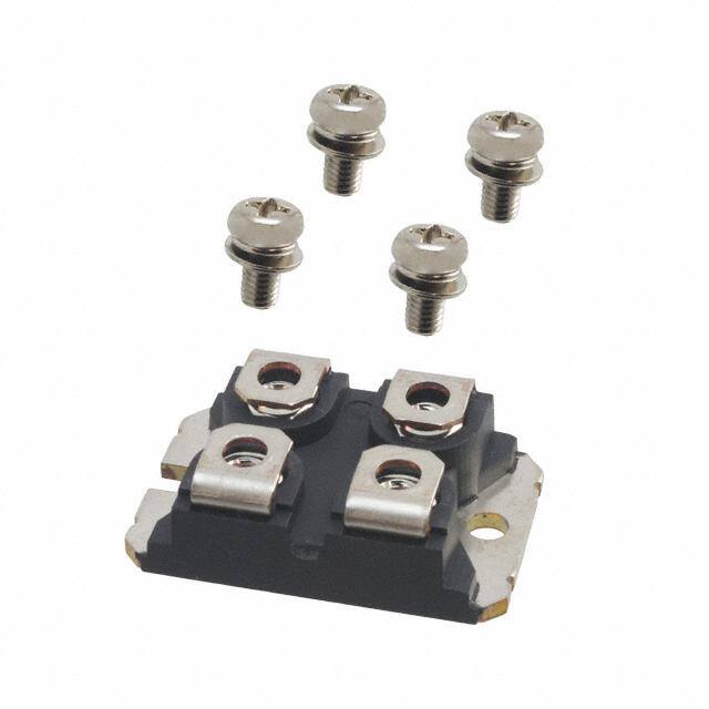
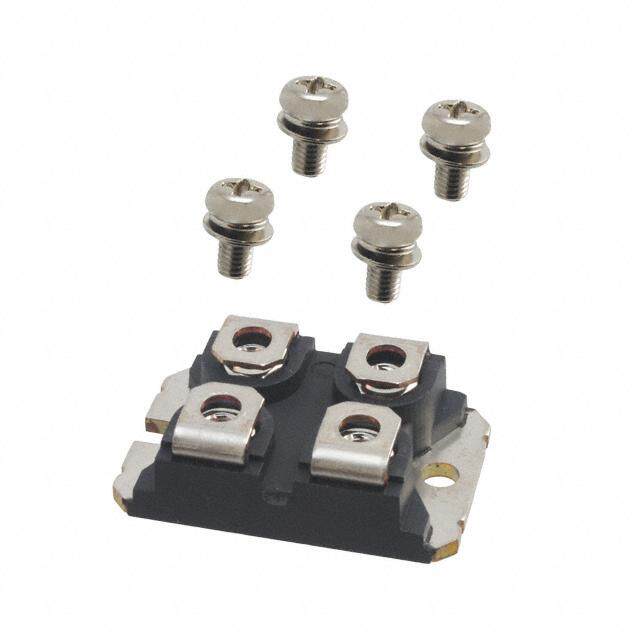
| 描述 | MOD THYRISTOR SGL 1200V SOT-227B |
| 产品分类 | SCR - 模块 |
| 品牌 | IXYS |
| 数据手册 | |
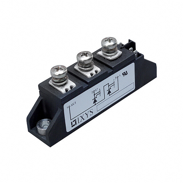
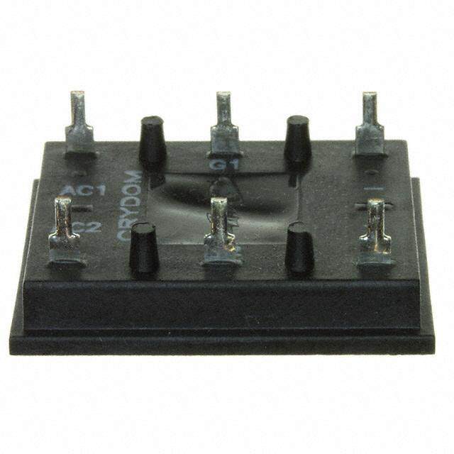
| 产品图片 |
|
| 产品型号 | MCO150-12IO1 |
| rohs | 无铅 / 符合限制有害物质指令(RoHS)规范要求 |
| SCR数,二极管 | 1 SCR |
| 产品系列 | - |
| 其它名称 | MCO15012IO1 |
| 包装 | 管件 |
| 安装类型 | 底座安装 |
| 封装/外壳 | SOT-227-4,miniBLOC |
| 标准包装 | 10 |
| 电压-断态 | 1200V |
| 电流-不重复浪涌50、60Hz(Itsm) | 2000A,2150A |
| 电流-保持(Ih)(最大值) | 200mA |
| 电流-栅极触发(Igt)(最大值) | 150mA |
| 电流-通态(It(AV))(最大值) | 149A |
| 电流-通态(It(RMS))(最大值) | 234A |
| 结构 | 单一 |


PDF Datasheet 数据手册内容提取
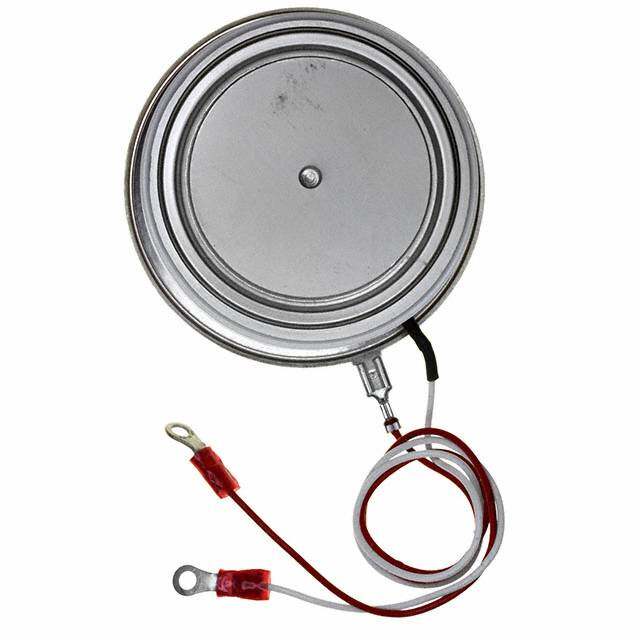
MCO150-12io1 Thyristor V = 1200V RRM I = 158A TAV V = 1,37V T Single Thyristor Part number MCO150-12io1 Backside: isolated 3 1/4 2 Features / Advantages: Applications: Package: SOT-227B (minibloc) ● Thyristor for line frequency ● Line rectifying 50/60 Hz ● Isolation Voltage: 3 0 0 0 V~ ● Planar passivated chip ● Softstart AC motor control ● Industry standard outline ● Long-term stability ● DC Motor control ● RoHS compliant ● Power converter ● Epoxy meets UL 94V-0 ● AC power control ● Base plate: Copper ● Lighting and temperature control internally DCB isolated ● Advanced power cycling Terms Conditions of usage: The data contained in this product data sheet is exclusively intended for technically trained staff. The user will have to evaluate the suitability of the product for the intended application and the completeness of the product data with respect to his application. The specifications of our components may not be considered as an assurance of component characteristics. The information in the valid application- and assembly notes must be considered. Should you require product information in excess of the data given in this product data sheet or which concerns the specific application of your product, please contact the sales office, which is responsible for you. Due to technical requirements our product may contain dangerous substances. For information on the types in question please contact the sales office, which is responsible for you. Should you intend to use the product in aviation, in health or live endangering or life support applications, please notify. For any such application we urgently recommend - to perform joint risk and quality assessments; - the conclusion of quality agreements; - to establish joint measures of an ongoing product survey, and that we may make delivery dependent on the realization of any such measures. IXYS reserves the right to change limits, conditions and dimensions. Data according to IEC 60747and per semiconductor unless otherwise specified 20150827b ©2015 IXYS all rights reserved
MCO150-12io1 Thyristor Ratings Symbol Definition Conditions min. typ. max. Unit V max. non-repetitive reverse/forward blocking voltage T = 25°C 1300 V RSM/DSM VJ V max. repetitive reverse/forward blocking voltage T = 25°C 1200 V RRM/DRM VJ I reverse current, drain current V = 1 2 0 0 V T = 25°C 100 µA R/D R/D VJ V = 1 2 0 0 V T = 1 2 5 °C 10 mA R/D VJ V forward voltage drop I = 1 5 0 A T = 25°C 1,37 V T T VJ I = 3 0 0 A 1,78 V T I = 1 5 0 A T = 1 2 5 °C 1,37 V T VJ I = 3 0 0 A 1,89 V T I average forward current T = 8 0 °C T = 1 5 0 °C 158 A TAV C VJ I RMS forward current 180° sine 250 A T(RMS) V threshold voltage T = 1 5 0 °C 0,84 V T0 VJ for power loss calculation only r slope resistance 3,5 mΩ T R thermal resistance junction to case 0,2 K/W thJC R thermal resistance case to heatsink 0,10 K/W thCH P total power dissipation T = 25°C 620 W tot C I max. forward surge current t = 10 ms; (50 Hz), sine T = 45°C 2,00 kA TSM VJ t = 8,3 ms; (60 Hz), sine V = 0 V 2,16 kA R t = 10 ms; (50 Hz), sine T = 1 5 0 °C 1,70 kA VJ t = 8,3 ms; (60 Hz), sine V = 0 V 1,84 kA R I²t value for fusing t = 10 ms; (50 Hz), sine T = 45°C 20,0 kA²s VJ t = 8,3 ms; (60 Hz), sine V = 0 V 19,4 kA²s R t = 10 ms; (50 Hz), sine T = 1 5 0 °C 14,5 kA²s VJ t = 8,3 ms; (60 Hz), sine V = 0 V 14,0 kA²s R C junction capacitance V = 4 0 0 V f = 1 MHz T = 25°C 119 pF J R VJ P max. gate power dissipation t = 30 µs T = 1 5 0 °C 10 W GM P C t = 300µs 5 W P P average gate power dissipation 0,5 W GAV (di/dt) critical rate of rise of current T =150°C; f = 50 Hz repetitive, I = 450A 150 A/µs cr VJ T t = 2 0 0 µs;di /dt=0,45 A/µs; P G I = 0,45A;V = ⅔ V non-repet., I = 150A 500 A/µs G DRM T (dv/dt) critical rate of rise of voltage V = ⅔ V T = 150°C 1000 V/µs cr DRM VJ R = ∞; method 1 (linear voltage rise) GK V gate trigger voltage V = 6 V T = 25°C 1,4 V GT D VJ T = -40°C 1,6 V VJ I gate trigger current V = 6 V T = 25°C 150 mA GT D VJ T = -40°C 200 mA VJ V gate non-trigger voltage V = ⅔ V T =150°C 0,2 V GD D DRM VJ I gate non-trigger current 10 mA GD I latching current t = 10 µs T = 25°C 450 mA L p VJ I = 0,45A; di /dt = 0,45A/µs G G I holding current V = 6 V R = ∞ T = 25°C 200 mA H D GK VJ t gate controlled delay time V = ½ V T = 25°C 2 µs gd D DRM VJ I = 0,45A; di /dt = 0,45A/µs G G t turn-off time V =100V; I =150A;V = ⅔ V T =125°C 150 µs q R T DRM VJ di/dt = 10A/µs dv/dt = 15V/µs t =200µs p IXYS reserves the right to change limits, conditions and dimensions. Data according to IEC 60747and per semiconductor unless otherwise specified 20150827b ©2015 IXYS all rights reserved
MCO150-12io1 Package SOT-227B (minibloc) Ratings Symbol Definition Conditions min. typ. max. Unit I RMS current per terminal 1) 150 A RMS T virtual junction temperature -40 150 °C VJ T operation temperature -40 125 °C op T storage temperature -40 150 °C stg Weight 30 g M mounting torque 1,1 1,5 Nm D M terminal torque 1,1 1,5 Nm T d terminal to terminal 10,5 3,2 mm Spp/App creepage distance on surface | striking distance through air d terminal to backside 8,6 6,8 mm Spb/Apb V isolation voltage t = 1 second 3000 V ISOL 50/60 Hz, RMS; II S O L ≤ 1 mA t = 1 minute 2500 V 1)IRMS is typically limited by the pin-to-chip resistance (1); or by the current capability of the chip (2). In case of (1) and a product with multiple pins for one chip-potential, the current capability can be increased by connecting the pins as one contact. Product Marking Part No. Logo XXXXX ® Zyyww abcd Assembly Line DateCode Assembly Code Ordering Ordering Number Marking on Product Delivery Mode Quantity Code No. Standard MCO150-12io1 MCO150-12io1 Tube 10 496332 Equivalent Circuits for Simulation * on die level T V J =150°C I V R Thyristor 0 0 V threshold voltage 0,84 V 0 max R slope resistance * 1,6 mΩ 0 max IXYS reserves the right to change limits, conditions and dimensions. Data according to IEC 60747and per semiconductor unless otherwise specified 20150827b ©2015 IXYS all rights reserved
MCO150-12io1 Outlines SOT-227B (minibloc) 3 1/4 2 IXYS reserves the right to change limits, conditions and dimensions. Data according to IEC 60747and per semiconductor unless otherwise specified 20150827b ©2015 IXYS all rights reserved
MCO150-12io1 Thyristor 300 1800 25000 50Hz,80%VRRM VR=0V 250 1600 20000 200 1400 I2t I ITSM TVJ=45°C 15000 T T =45°C 150 1200 [A2s] VJ [A] [A] 10000 100 1000 T =125°C VJ T =125°C VJ 125°C 5000 50 800 150°C T =25°C VJ 0 600 0 0,4 0,8 1,2 1,6 2,0 0,01 0,1 1 1 2 3 4 5 6 78910 V [V] t [s] t [ms] T Fig.1 Forwardcharacteristics Fig.2 Surgeoverloadcurrent Fig.3 I2tversus time(1-10ms) 10 1000 300 1:IGD,TVJ=125°C dc= 2:IGT,TVJ= 25°C 1 3:IGT,TVJ= -40°C 250 0.5 6 0.4 5 0.33 4 100 200 0.17 VG 23 tgd typ. Limit IT(AV)M 0.08 1 1 150 [V] [µs] [A] 10 100 TVJ=125°C 50 4:PGAV=0.5W IGD,TVJ=125°C 5:PGM= 5W 0,1 6:PGM= 10W 1 0 1 10 100 1000 10000 10 100 1000 0 25 50 75 100 125 150 I [mA] I [mA] T [°C] G G C Fig.4 Gate triggercharacteristics Fig.5 Gatecontrolleddelay time Fig.6 Max. forwardcurrent atcase temperature 350 dc= 300 1 RthHA 0,20 0.5 0.1 0.4 0.2 250 0.33 0.4 0.17 0.6 0,15 200 0.08 0.8 Z P 1.0 thJC (AV) 150 0,10 R [K/W] t [s] thi i [W] [K/W] 0.020 0.030 100 0.023 0.003 0,05 0.032 0.050 50 0.043 0.250 0.082 0.170 0 0,00 0 40 80 120 160 200 0 50 100 150 100 101 102 103 104 I [A] T [°C] t [ms] T(AV) amb Fig.7a Powerdissipationversusdirectoutputcurrent Fig.8 Transient thermalimpedancejunction tocase Fig.7b andambient temperature IXYS reserves the right to change limits, conditions and dimensions. Data according to IEC 60747and per semiconductor unless otherwise specified 20150827b ©2015 IXYS all rights reserved
Mouser Electronics Authorized Distributor Click to View Pricing, Inventory, Delivery & Lifecycle Information: I XYS: MCO150-12io1