ICGOO在线商城 > 集成电路(IC) > PMIC - 稳压器 - 线性 > MC79L05ACDR2G
 Datasheet下载
- 型号: MC79L05ACDR2G
- 制造商: ON Semiconductor
- 库位|库存: xxxx|xxxx
- 要求:
| 数量阶梯 | 香港交货 | 国内含税 |
| +xxxx | $xxxx | ¥xxxx |
查看当月历史价格
查看今年历史价格
MC79L05ACDR2G产品简介:
ICGOO电子元器件商城为您提供MC79L05ACDR2G由ON Semiconductor设计生产,在icgoo商城现货销售,并且可以通过原厂、代理商等渠道进行代购。 MC79L05ACDR2G价格参考¥0.63-¥0.63。ON SemiconductorMC79L05ACDR2G封装/规格:PMIC - 稳压器 - 线性, Linear Voltage Regulator IC Negative Fixed 1 Output -5V 100mA 8-SOIC。您可以下载MC79L05ACDR2G参考资料、Datasheet数据手册功能说明书,资料中有MC79L05ACDR2G 详细功能的应用电路图电压和使用方法及教程。
MC79L05ACDR2G 是由 ON Semiconductor(现为安森美半导体)生产的一款线性稳压器,属于 PMIC(电源管理集成电路)系列。该器件的主要应用场景包括:

1. 消费电子设备:如智能手机、平板电脑、便携式音频设备等。这些设备通常需要稳定的电压供应来确保内部电路的正常工作,MC79L05ACDR2G 可以为这些设备中的微控制器、传感器和其他低功耗组件提供稳定的 5V 输出电压。

2. 工业自动化和控制:在工业环境中,各种传感器、执行器和通信模块需要稳定可靠的电源。MC79L05ACDR2G 可以用于为这些模块供电,确保它们在复杂的工作环境下依然能够稳定运行。

3. 医疗设备:例如便携式医疗仪器、心率监测器、血糖仪等。这些设备对电源的稳定性和可靠性要求极高,MC79L05ACDR2G 的低噪声和高精度输出特性使其非常适合用于这些应用。

4. 汽车电子系统:如车载信息娱乐系统、导航设备、传感器等。汽车环境中的电源波动较大,MC79L05ACDR2G 的宽输入电压范围和良好的瞬态响应能力可以确保这些设备在不同工况下都能获得稳定的电源。

5. 物联网(IoT)设备:如智能家居设备、智能计量表、无线传感器节点等。这些设备通常需要长时间稳定工作,MC79L05ACDR2G 的低功耗特性和高效能使其成为理想的选择。

6. 嵌入式系统:在各种嵌入式控制系统中,MC79L05ACDR2G 可以为微处理器、内存芯片和其他外围设备提供稳定的电源,确保系统的可靠性和稳定性。

总之,MC79L05ACDR2G 由于其出色的性能和广泛的应用范围,成为了许多低功耗、高精度电源需求场景下的首选稳压器。
| 参数 | 数值 |
| 产品目录 | 集成电路 (IC)半导体 |
| 描述 | IC REG LDO -5V 0.1A 8SOIC线性稳压器 5V 100mA Negative |
| 产品分类 | |
| 品牌 | ON Semiconductor |
| 产品手册 | |
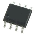
| 产品图片 |
|
| rohs | 符合RoHS无铅 / 符合限制有害物质指令(RoHS)规范要求 |
| 产品系列 | 电源管理 IC,线性稳压器,ON Semiconductor MC79L05ACDR2G- |
| 数据手册 | |
| 产品型号 | MC79L05ACDR2G |
| PCN组件/产地 | |
| PSRR/纹波抑制—典型值 | 49 dB |
| 产品目录页面 | |
| 产品种类 | |
| 供应商器件封装 | 8-SOIC N |
| 其它名称 | MC79L05ACDR2GOSTR |
| 包装 | 带卷 (TR) |
| 商标 | ON Semiconductor |
| 安装类型 | 表面贴装 |
| 安装风格 | SMD/SMT |
| 封装 | Reel |
| 封装/外壳 | 8-SOIC(0.154",3.90mm 宽) |
| 封装/箱体 | SOIC-8 |
| 工作温度 | 0°C ~ 125°C |
| 工厂包装数量 | 2500 |
| 最大工作温度 | + 125 C |
| 最大输入电压 | - 30 V |
| 最小工作温度 | 0 C |
| 最小输入电压 | - 7 V |
| 极性 | Negative |
| 标准包装 | 2,500 |
| 电压-跌落(典型值) | 1.7V @ 40mA |
| 电压-输入 | 可下调至 -30V |
| 电压-输出 | -5V |
| 电流-输出 | 100mA |
| 电流-限制(最小值) | - |
| 稳压器拓扑 | 负,固定式 |
| 稳压器数 | 1 |
| 系列 | MC79L05 |
| 线路调整率 | 150 mV |
| 负载调节 | 60 mV |
| 输出电压 | - 5 V |
| 输出电流 | 0.1 A |
| 输出端数量 | 1 |
| 输出类型 | Fixed |


- 商务部:美国ITC正式对集成电路等产品启动337调查
- 曝三星4nm工艺存在良率问题 高通将骁龙8 Gen1或转产台积电
- 太阳诱电将投资9.5亿元在常州建新厂生产MLCC 预计2023年完工
- 英特尔发布欧洲新工厂建设计划 深化IDM 2.0 战略
- 台积电先进制程称霸业界 有大客户加持明年业绩稳了
- 达到5530亿美元!SIA预计今年全球半导体销售额将创下新高
- 英特尔拟将自动驾驶子公司Mobileye上市 估值或超500亿美元
- 三星加码芯片和SET,合并消费电子和移动部门,撤换高东真等 CEO
- 三星电子宣布重大人事变动 还合并消费电子和移动部门
- 海关总署:前11个月进口集成电路产品价值2.52万亿元 增长14.8%


PDF Datasheet 数据手册内容提取
MC79L00A Series 100 mA Negative Voltage Regulators The MC79L00A Series negative voltage regulators are inexpensive, easy−to−use devices suitable for numerous applications requiring up to 100 mA. Like the higher powered MC7900 Series negative regulators, this series features thermal shutdown and current www.onsemi.com limiting, making them remarkably rugged. In most applications, no external components are required for operation. THREE−TERMINAL LOW The MC79L00A devices are useful for on−card regulation or any CURRENT NEGATIVE FIXED other application where a regulated negative voltage at a modest VOLTAGE REGULATORS current level is needed. These regulators offer substantial advantage over the common resistor/Zener diode approach. MARKING Features DIAGRAMS • No External Components Required • Pin 1.Vout Internal Short Circuit Current Limiting 2.Vin 8 • Internal Thermal Overload Protection 8 3.Vin 9Lxxx • Low Cost SOIC1−8 45..NGCND ALY(cid:2)Wy • Complementary Positive Regulators Offered (MC78L00 Series) D SUFFIX 6.Vin 1 • CASE 751 7.Vin Pb−Free Packages are Available 8.NC TO−92 P SUFFIX CASE 29 1 GND 123 2 3 R8 R6 STRAIGHT LEAD BENT LEAD R Q10 BULK PACK TAPE & REEL 5 Q5 R9 AMMO PACK R18 R17 R1 Q4 Pin 1.Ground R7 2.Input MC79L Q8 Q14 3.Output xxxxx ALYW(cid:2) Q9 R16 (cid:2) Q1 R4 Output R2 Q12 Q13 Z1 C Q2 xxx = Specific Device Code R3 Q6 Q7 Q11 A = Assembly Location R10 R11 R14 R15 L = Wafer Lot Y = Year Input W = Work Week *(cid:2)Automotive temperature range selections are available with special test conditions y = B or C and additional tests in 5, 12 and 15 V devices. Contact your local ON Semiconductor (cid:2) = Pb−Free Package sales office for information. (Note: Microdot may be in either location) Figure 1. Representative Schematic Diagram ORDERING INFORMATION See detailed ordering and shipping information in the package dimensions section on page 7 of this data sheet. © Semiconductor Components Industries, LLC, 1994 1 Publication Order Number: October, 2016 − Rev. 10 MC79L00/D
MC79L00A Series MAXIMUM RATINGS (TA = +25°C, unless otherwise noted.) Rating Symbol Value Unit Input Voltage (−5 V) VI −30 Vdc (−12, −15, −18 V) −35 (−24 V) −40 Power Dissipation Case 29 (TO−92 Type) TA = 25°C PD Internally Limited W Thermal Resistance, Junction−to−Ambient R(cid:2)JA 160 °C/W Thermal Resistance, Junction−to−Case R(cid:2)JC 83 °C/W Case 751 (SOIC−8 Type) (Note 1) TA = 25°C PD Internally Limited W Thermal Resistance, Junction−to−Ambient R(cid:2)JA 180 °C/W Thermal Resistance, Junction−to−Case R(cid:2)JC 45 °C/W Storage Temperature Range Tstg −65 to +150 °C Junction Temperature TJ +150 °C Stresses exceeding those listed in the Maximum Ratings table may damage the device. If any of these limits are exceeded, device functionality should not be assumed, damage may occur and reliability may be affected. 1. SOIC−8 Junction−to−Ambient Thermal Resistance is for minimum recommended pad size. Refer to Figure 9 for Thermal Resistance variation versus pad size. *This device series contains ESD protection and exceeds the following tests: Human Body Model 2000 V per MIL_STD_883, Method 3015 Machine Model Method 200 V. ELECTRICAL CHARACTERISTICS (VI = −10 V, IO = 40 mA, CI = 0.33 (cid:3)F, CO = 0.1 (cid:3)F, −40°C < TJ +125°C (for MC79LXXAB), 0°C < TJ < +125°C (for MC79LXXAC)). MC79L05AC, AB Characteristics Symbol Min Typ Max Unit Output Voltage (TJ = +25°C) VO −4.8 −5.0 −5.2 Vdc Input Regulation (TJ = +25°C) Regline mV −7.0 Vdc ≥ VI ≥ −20 Vdc − − 150 −8.0 Vdc ≥ VI ≥ −20 Vdc − − 100 Load Regulation Regload mV TJ = +25°C, 1.0 mA ≤ IO ≤ 100 mA − − 60 1.0 mA ≤ IO ≤ 40 mA − − 30 Output Voltage VO Vdc −7.0 Vdc ≥ VI ≥ −20 Vdc, 1.0 mA ≤ IO ≤ 40 mA −4.75 − −5.25 VI = −10 Vdc, 1.0 mA ≤ IO ≤ 70 mA −4.75 − −5.25 Input Bias Current IIB mA (TJ = +25°C) − − 6.0 (TJ = +125°C) − − 5.5 Input Bias Current Change IIB mA −8.0 Vdc ≥ VI ≥ −20 Vdc − − 1.5 1.0 mA ≤ IO ≤ 40 mA − − 0.1 Output Noise Voltage (TA = +25°C, 10 Hz ≤ f ≤ 100 kHz) Vn − 40 − (cid:3)V Ripple Rejection (−8.0 ≥ VI ≥ −18 Vdc, f = 120 Hz, TJ = +25°C) RR 41 49 − dB Dropout Voltage (IO = 40 mA, TJ = +25°C) |VI−VO| − 1.7 − Vdc Product parametric performance is indicated in the Electrical Characteristics for the listed test conditions, unless otherwise noted. Product performance may not be indicated by the Electrical Characteristics if operated under different conditions. www.onsemi.com 2
MC79L00A Series ELECTRICAL CHARACTERISTICS (VI = −19 V, IO = 40 mA, CI = 0.33 (cid:3)F, CO = 0.1 (cid:3)F, −40°C < TJ +125°C (for MC79LXXAB), 0°C < TJ < +125°C (for MC79LXXAC)). MC79L12AC, AB Characteristics Symbol Min Typ Max Unit Output Voltage (TJ = +25°C) VO −11.5 −12 −12.5 Vdc Input Regulation (TJ = +25°C) Regline mV −14.5 Vdc ≥ VI ≥ −27 Vdc − − 250 −16 Vdc ≥ VI ≥ −27 Vdc − − 200 Load Regulation Regload 100 mV TJ = +25°C, 1.0 mA ≤ IO ≤ 100 mA − − 50 1.0 mA ≤ IO ≤ 40 mA − − Output Voltage VO −11.4 −12.6 Vdc −14.5 Vdc ≥ VI ≥ −27 Vdc, 1.0 mA ≤ IO ≤ 40 mA −11.4 − −12.6 VI = −19 Vdc, 1.0 mA ≤ IO ≤ 70 mA − Input Bias Current IIB mA (TJ = +25°C) − − 6.5 (TJ = +125°C) − − 6.0 Input Bias Current Change IIB 1.5 mA −16 Vdc ≥ VI ≥ −27 Vdc − − 0.2 1.0 mA ≤ IO ≤ 40 mA − − Output Noise Voltage (TA = +25°C, 10 Hz ≤ f ≤ 100 kHz) Vn − 80 − (cid:3)V Ripple Rejection (−15 ≤ VI ≤ −25 Vdc, f = 120 Hz, TJ = +25°C) RR 37 42 − dB Dropout Voltage (IO = 40 mA, TJ = +25°C) |VI−VO| − 1.7 − Vdc Product parametric performance is indicated in the Electrical Characteristics for the listed test conditions, unless otherwise noted. Product performance may not be indicated by the Electrical Characteristics if operated under different conditions. ELECTRICAL CHARACTERISTICS (VI = −23 V, IO = 40 mA, CI = 0.33 (cid:3)F, CO = 0.1 (cid:3)F, −40°C < TJ +125°C (for MC79LXXAB), 0°C < TJ < +125°C (for MC79LXXAC)). MC79L15AC, AB Characteristics Symbol Min Typ Max Unit Output Voltage (TJ = +25°C) VO −14.4 −15 −15.6 Vdc Input Regulation (TJ = +25°C) Regline mV −17.5 Vdc ≥ VI ≥ −30 Vdc − − 300 −20 Vdc ≥ VI ≥ −30 Vdc − − 250 Load Regulation Regload mV TJ = +25°C, 1.0 mA ≤ IO ≤ 100 mA − − 150 1.0 mA ≤ IO ≤ 40 mA − − 75 Output Voltage VO Vdc −17.5 Vdc ≥ VI ≥ −Vdc, 1.0 mA ≤ IO ≤ 40 mA −14.25 − −15.75 VI = −23 Vdc, 1.0 mA ≤ IO ≤ 70 mA −14.25 − −15.75 Input Bias Current IIB mA (TJ = +25°C) − − 6.5 (TJ = +125°C) − − 6.0 Input Bias Current Change (cid:4)IIB mA −20 Vdc ≥ VI ≥ −30 Vdc − − 1.5 1.0 mA ≤ IO ≤ 40 mA − − 0.1 Output Noise Voltage (TA = +25°C, 10 Hz ≤ f ≤ 100 kHz) VN − 90 − (cid:3)V Ripple Rejection (−18.5 ≤ VI ≤ −28.5 Vdc, f = 120 Hz) RR 34 39 − dB Dropout Voltage IO = 40 mA, TJ = +25°C |VI−VO| − 1.7 − Vdc Product parametric performance is indicated in the Electrical Characteristics for the listed test conditions, unless otherwise noted. Product performance may not be indicated by the Electrical Characteristics if operated under different conditions. www.onsemi.com 3
MC79L00A Series ELECTRICAL CHARACTERISTICS (VI = −27 V, IO = 40 mA, CI = 0.33 (cid:3)F, CO = 0.1 (cid:3)F, −40°C < TJ +125°C (for MC79LXXAB), 0°C < TJ < +125°C (for MC79LXXAC), unless otherwise noted). MC79L18AC Characteristics Symbol Min Typ Max Unit Output Voltage (TJ = +25°C) VO −17.3 −18 −18.7 Vdc Input Regulation (TJ = +25°C) Regline mV −20.7 Vdc ≥ VI ≥ −33 Vdc − − 325 −21.4 Vdc ≥ VI ≥ −33 Vdc − − − −22 Vdc ≥ VI ≥ −33 Vdc − − − −21 Vdc ≥ VI ≥ −33 Vdc − − 275 Load Regulation Regload mV TJ = +25°C, 1.0 mA ≤ IO ≤ 100 mA − − 170 1.0 mA ≤ IO ≤ 40 mA − − 85 Output Voltage VO Vdc −20.7 Vdc ≥ VI ≥ −33 Vdc, 1.0 mA ≤ IO ≤ 40 mA −17.1 − −18.9 −21.4 Vdc ≥ VI ≥ −33 Vdc, 1.0 mA ≤ IO ≤ 40 mA − − − VI = −27 Vdc, 1.0 mA ≤ IO ≤ 70 mA −17.1 − −18.9 Input Bias Current IIB mA (TJ = +25°C) − − 6.5 (TJ = +125°C) − − 6.0 Input Bias Current Change IIB mA −21 Vdc ≥ VI ≥ −33 Vdc − − 1.5 −27 Vdc ≥ VI ≥ −33 Vdc − − − 1.0 mA ≤ IO ≤ 40 mA − − 0.1 Output Noise Voltage (TA = +25°C, 10 Hz ≤ f ≤ 100 kHz) Vn − 150 − (cid:3)V Ripple Rejection (−23 ≤ VI ≤ −33 Vdc, f = 120 Hz, TJ = +25°C) RR 33 48 − dB Dropout Voltage IO = 40 mA, TJ = +25°C |VI−VO| − 1.7 − Vdc Product parametric performance is indicated in the Electrical Characteristics for the listed test conditions, unless otherwise noted. Product performance may not be indicated by the Electrical Characteristics if operated under different conditions. ELECTRICAL CHARACTERISTICS (VI = −33 V, IO = 40 mA, CI = 0.33 (cid:3)F, CO = 0.1 (cid:3)F, −40°C < TJ +125°C (for MC79LXXAB), 0°C < TJ < +125°C (for MC79LXXAC), unless otherwise noted). MC79L24AC Characteristics Symbol Min Typ Max Unit Output Voltage (TJ = +25°C) VO −23 −24 −25 Vdc Input Regulation (TJ = +25°C) Regline mV −27 Vdc ≥ VI ≥ −38 Vdc − − 350 −27.5 Vdc ≥ VI ≥ −38 Vdc − − − −28 Vdc ≥ VI ≥ −38 Vdc − − 300 Load Regulation Regload mV TJ = +25°C, 1.0 mA ≤ IO ≤ 100 mA − − 200 1.0 mA ≤ IO ≤ 40 mA − − 100 Output Voltage VO Vdc −27 Vdc ≥ VI ≥ −38 V, 1.0 mA ≤ IO ≤ 40 mA −22.8 − −25.2 −28 Vdc ≥ VI ≥ −38 Vdc, 1.0 mA ≤ IO ≤ 40 mA − − − VI = −33 Vdc, 1.0 mA ≤ IO ≤ 70 mA −22.8 − −25.2 Input Bias Current IIB mA (TJ = +25°C) − − 6.5 (TJ = +125°C) − − 6.0 Input Bias Current Change (cid:4)IIB mA −28 Vdc ≥ VI ≥ −38 Vdc − − 1.5 1.0 mA ≤ IO ≤ 40 mA − − 0.1 Output Noise Voltage (TA = +25°C, 10 Hz ≤ f ≤ 100 kHz) Vn − 200 − (cid:3)V Ripple Rejection (−29 ≤ VI ≤ −35 Vdc, f = 120 Hz, TJ = +25°C) RR 31 47 − dB Dropout Voltage IO = 40 mA, TJ = +25°C |VI−VO| − 1.7 − Vdc Product parametric performance is indicated in the Electrical Characteristics for the listed test conditions, unless otherwise noted. Product performance may not be indicated by the Electrical Characteristics if operated under different conditions. www.onsemi.com 4
MC79L00A Series APPLICATIONS INFORMATION Design Considerations high−frequency characteristics to insure stable operation The MC79L00A Series of fixed voltage regulators are under all load conditions. A 0.33 (cid:3)F or larger tantalum, designed with Thermal Overload Protections that shuts mylar, or other capacitor having low internal impedance at down the circuit when subjected to an excessive power high frequencies should be chosen. The bypass capacitor overload condition, Internal Short Circuit Protection that should be mounted with the shortest possible leads directly limits the maximum current the circuit will pass. across the regulator’s input terminals. Normally good In many low current applications, compensation construction techniques should be used to minimize ground capacitors are not required. However, it is recommended loops and lead resistance drops since the regulator has no that the regulator input be bypassed with a capacitor if the external sense lead. Bypassing the output is also regulator is connected to the power supply filter with long recommended. wire length, or if the output load capacitance is large. An input bypass capacitor should be selected to provide good Input MC79LXX Output +Vin MC78LXX +VO C0.I3*3(cid:3)F C0.O1*(cid:3)*F 0.33(cid:3)F 0.1(cid:3)F 0.1(cid:3)F A common ground is required between the input and the output -Vin MC79LXX -VO voltages. The input voltage must remain typically 2.0 V above the output voltage even during the low point on the ripple voltage. 0.33(cid:3)F (cid:3)* CI is required if regulator is located an appreciable (cid:3)* distance from the power supply filter ** CO improves stability and transient response. Figure 2. Positive and Negative Regulator Figure 3. Standard Application www.onsemi.com 5
MC79L00A Series TYPICAL CHARACTERISTICS (T = +25°C, unless otherwise noted.) A 8.0 L -2.5 A TI MC79L05C N GE (V) 6.0 VTJO == 2-55°.C0 V FFERE -2.0 IO = 70 mA UT VOLTA 4.0 IO = 1.0 mA IO = 100 mA UTPUT DIGE (V) -1.5 IO = 1.0 mA IO = 40 mA , OUTPO NPUT/OVOLTA -1.0 Dropout of Regulation is V 2.0 IO = 40 mA , IVO -0.5 d(cid:4)eVfiOn e=d 2w%h eonf VO - I V 0 0 0 -2.0 -4.0 -6.0 -0.8 -10 0 25 50 75 100 125 Vin, INPUT VOLTAGE (V) TJ, JUNCTION TEMPERATURE (°C) Figure 4. Dropout Characteristics Figure 5. Dropout Voltage versus Junction Temperature 4.2 5.0 A) A) m 4.0 m T ( T ( 4.0 N N RE 3.8 RE R R CU 3.6 CU 3.0 S S MC79L05C A A UT BI 3.4 UT BI 2.0 VIOO = = 4 -05 m.0A V P MC79L05C P I, INIB3.2 VViOn == --150.0 V V I, INIB 1.0 3.0 IO = 40 mA 0 0 0 25 50 75 100 125 0 -5.0 -10 -15 -20 -25 -30 -35 -40 TA, AMBIENT TEMPERATURE (°C) Vin, INPUT VOLTAGE (V) Figure 6. Input Bias Current versus Figure 7. Input Bias Current versus Ambient Temperature Input Voltage 10,000 170 3.2 W) , POWER DISSIPATION (mW)PD1,01100000 RPD(cid:2)(JmAa =x) 2to0 02°5C°/CW = 625 mWNo Heatsink R, THERMAL RESISTANCEθJA°JUNCTION-TO-AIR (C/W)11135357910000000 R(cid:2)JA ÎÎGLrapÎÎhCP2 r.Doe0p(Lp mÎÎÎÎopraezex.sr) efonÎÎrt sT Asy =ÎÎÎÎm +m5e0ÎÎt°riCca3l ÎÎ.l0a ymoumt 0011222.......4826048P, MAXIMUM POWER DISSIPATION (D 25 50 75 100 125 150 0 10 20 30 40 50 TA, AMBIENT TEMPERATURE (°C) L, LENGTH OF COPPER (mm) Figure 8. Maximum Average Power Dissipation Figure 9. SOP−8 Thermal Resistance and Maximum versus Ambient Temperature (TO−92) Power Dissipation versus P.C.B. Copper Length www.onsemi.com 6
MC79L00A Series ORDERING INFORMATION Device Nominal Operating Temperature Package Shipping† Voltage Range MC79L05ABDG −5.0 V TJ = −40° to +125°C SOIC−8 98 Units / Rail (Pb−Free) MC79L05ABDR2G SOIC−8 2500 / Tape & Reel (Pb−Free) MC79L05ABPG TO−92 2000 Units / Bag (Pb−Free) MC79L05ABPRAG TO−92 2000 / Tape & Reel (Pb−Free) MC79L05ACDG TJ = 0° to +125°C SOIC−8 98 Units / Rail (Pb−Free) MC79L05ACDR2G SOIC−8 2500 / Tape & Reel (Pb−Free) MC79L05ACPG TO−92 2000 Units / Bag (Pb−Free) MC79L05ACPRAG TO−92 2000 / Tape & Reel (Pb−Free) MC79L05ACPRMG TO−92 2000 / Tape & Ammo Box (Pb−Free) MC79L05ACPRPG TO−92 2000 / Tape & Ammo Box (Pb−Free) MC79L12ABDG −12 V TJ = −40° to +125°C SOIC−8 98 Units / Rail (Pb−Free) MC79L12ABDR2G SOIC−8 2500 / Tape & Reel (Pb−Free) MC79L12ABPG TO−92 2000 Units / Bag (Pb−Free) MC79L12ABPRAG TO−92 2000 / Tape & Reel (Pb−Free) MC79L12ACDG −12 V TJ = 0° to +125°C SOIC−8 98 Units / Rail (Pb−Free) MC79L12ACDR2G SOIC−8 2500 / Tape & Reel (Pb−Free) MC79L12ACPG TO−92 2000 Units / Bag (Pb−Free) MC79L12ACPRAG TO−92 2000 / Tape & Reel (Pb−Free) MC79L12ACPRPG TO−92 2000 / Tape & Ammo Box (Pb−Free) www.onsemi.com 7
MC79L00A Series ORDERING INFORMATION (continued) Device Nominal Operating Temperature Package Shipping† Voltage Range MC79L15ABDG −15 V TJ = −40° to +125°C SOIC−8 98 Units / Rail (Pb−Free) MC79L15ABDR2G SOIC−8 2500 / Tape & Reel (Pb−Free) MC79L15ABPG TO−92 2000 Units / Bag (Pb−Free) MC79L15ABPRPG TO−92 2000 / Tape & Ammo Box (Pb−Free) MC79L15ACDG TJ = 0° to +125°C SOIC−8 98 Units / Rail (Pb−Free) MC79L15ACDR2G SOIC−8 2500 / Tape & Reel (Pb−Free) MC79L15ACPG TO−92 2000 Units / Bag (Pb−Free) MC79L15ACPRAG TO−92 2000 / Tape & Reel (Pb−Free) MC79L15ACPREG TO−92 2000 / Tape & Reel (Pb−Free) MC79L15ACPRPG TO−92 2000 / Tape & Ammo Box (Pb−Free) MC79L18ABPRPG −18 V TJ = −40° to +125°C TO−92 2000 / Tape & Ammo Box (Pb−Free) MC79L18ACPG TJ = 0° to +125°C TO−92 2000 Units / Bag (Pb−Free) MC79L24ABPG −24 V TJ = −40° to +125°C TO−92 2000 Units / Bag (Pb−Free) MC79L24ACPG TJ = 0° to +125°C TO−92 2000 Units / Bag (Pb−Free) MC79L24ACPRMG TO−92 2000 / Tape & Ammo Box (Pb−Free) MC79L24ACPRPG TO−92 2000 / Tape & Ammo Box (Pb−Free) †For information on tape and reel specifications, including part orientation and tape sizes, please refer to our Tape and Reel Packaging Specifications Brochure, BRD8011/D. www.onsemi.com 8
MC79L00A Series PACKAGE DIMENSIONS SOIC−8 NB CASE 751−07 ISSUE AK NOTES: −X− 1. DIMENSIONING AND TOLERANCING PER ANSI Y14.5M, 1982. A 2. CONTROLLING DIMENSION: MILLIMETER. 3. DIMENSION A AND B DO NOT INCLUDE MOLD PROTRUSION. 4. MAXIMUM MOLD PROTRUSION 0.15 (0.006) 8 5 PER SIDE. 5. DIMENSION D DOES NOT INCLUDE DAMBAR B S 0.25 (0.010) M Y M PROTRUSION. ALLOWABLE DAMBAR PROTRUSION SHALL BE 0.127 (0.005) TOTAL 1 IN EXCESS OF THE D DIMENSION AT −Y− 4 K 6. M75A1X−I0M1U TMH RMUA T7E51R−IA06L CAROEN DOIBTSIOONL.ETE. NEW STANDARD IS 751−07. G MILLIMETERS INCHES DIM MIN MAX MIN MAX A 4.80 5.00 0.189 0.197 C NX 45(cid:3) B 3.80 4.00 0.150 0.157 SEATING C 1.35 1.75 0.053 0.069 PLANE D 0.33 0.51 0.013 0.020 −Z− G 1.27 BSC 0.050 BSC H 0.10 0.25 0.004 0.010 0.10 (0.004) J 0.19 0.25 0.007 0.010 H D M J K 0.40 1.27 0.016 0.050 M 0 (cid:3) 8 (cid:3) 0 (cid:3) 8 (cid:3) N 0.25 0.50 0.010 0.020 0.25 (0.010)M Z Y S X S S 5.80 6.20 0.228 0.244 SOLDERING FOOTPRINT* 1.52 0.060 7.0 4.0 0.275 0.155 0.6 1.270 0.024 0.050 (cid:2) (cid:3) mm SCALE 6:1 inches *For additional information on our Pb−Free strategy and soldering details, please download the ON Semiconductor Soldering and Mounting Techniques Reference Manual, SOLDERRM/D. www.onsemi.com 9
MC79L00A Series PACKAGE DIMENSIONS TO−92 (TO−226) CASE 29−11 ISSUE AM A NOTES: B STRAIGHT LEAD 1. DIMENSIONING AND TOLERANCING PER ANSI BULK PACK Y14.5M, 1982. 2. CONTROLLING DIMENSION: INCH. R 3. CONTOUR OF PACKAGE BEYOND DIMENSION R IS UNCONTROLLED. P 4. LEAD DIMENSION IS UNCONTROLLED IN P AND BEYOND DIMENSION K MINIMUM. L SEATING INCHES MILLIMETERS PLANE K DIM MIN MAX MIN MAX A 0.175 0.205 4.45 5.20 B 0.170 0.210 4.32 5.33 C 0.125 0.165 3.18 4.19 D 0.016 0.021 0.407 0.533 X X D G 0.045 0.055 1.15 1.39 G H 0.095 0.105 2.42 2.66 J 0.015 0.020 0.39 0.50 H J K 0.500 --- 12.70 --- L 0.250 --- 6.35 --- V C N 0.080 0.105 2.04 2.66 P --- 0.100 --- 2.54 SECTION X−X R 0.115 --- 2.93 --- 1 N V 0.135 --- 3.43 --- N R A B BENT LEAD N1O.TEDSIM:ENSIONING AND TOLERANCING PER TAPE & REEL ASME Y14.5M, 1994. 2. CONTROLLING DIMENSION: AMMO PACK MILLIMETERS. 3. CONTOUR OF PACKAGE BEYOND P DIMENSION R IS UNCONTROLLED. 4. LEAD DIMENSION IS UNCONTROLLED IN T P AND BEYOND DIMENSION K MINIMUM. MILLIMETERS SPELAATNIENG K DIM MIN MAX A 4.45 5.20 B 4.32 5.33 C 3.18 4.19 D 0.40 0.54 X X D G 2.40 2.80 G J 0.39 0.50 K 12.70 --- J N 2.04 2.66 V P 1.50 4.00 C R 2.93 --- V 3.43 --- SECTION X−X 1 N ON Semiconductor and are trademarks of Semiconductor Components Industries, LLC dba ON Semiconductor or its subsidiaries in the United States and/or other countries. ON Semiconductor owns the rights to a number of patents, trademarks, copyrights, trade secrets, and other intellectual property. A listing of ON Semiconductor’s product/patent coverage may be accessed at www.onsemi.com/site/pdf/Patent−Marking.pdf. ON Semiconductor reserves the right to make changes without further notice to any products herein. ON Semiconductor makes no warranty, representation or guarantee regarding the suitability of its products for any particular purpose, nor does ON Semiconductor assume any liability arising out of the application or use of any product or circuit, and specifically disclaims any and all liability, including without limitation special, consequential or incidental damages. Buyer is responsible for its products and applications using ON Semiconductor products, including compliance with all laws, regulations and safety requirements or standards, regardless of any support or applications information provided by ON Semiconductor. “Typical” parameters which may be provided in ON Semiconductor data sheets and/or specifications can and do vary in different applications and actual performance may vary over time. All operating parameters, including “Typicals” must be validated for each customer application by customer’s technical experts. ON Semiconductor does not convey any license under its patent rights nor the rights of others. ON Semiconductor products are not designed, intended, or authorized for use as a critical component in life support systems or any FDA Class 3 medical devices or medical devices with a same or similar classification in a foreign jurisdiction or any devices intended for implantation in the human body. Should Buyer purchase or use ON Semiconductor products for any such unintended or unauthorized application, Buyer shall indemnify and hold ON Semiconductor and its officers, employees, subsidiaries, affiliates, and distributors harmless against all claims, costs, damages, and expenses, and reasonable attorney fees arising out of, directly or indirectly, any claim of personal injury or death associated with such unintended or unauthorized use, even if such claim alleges that ON Semiconductor was negligent regarding the design or manufacture of the part. ON Semiconductor is an Equal Opportunity/Affirmative Action Employer. This literature is subject to all applicable copyright laws and is not for resale in any manner. PUBLICATION ORDERING INFORMATION LITERATURE FULFILLMENT: N. American Technical Support: 800−282−9855 Toll Free ON Semiconductor Website: www.onsemi.com Literature Distribution Center for ON Semiconductor USA/Canada 19521 E. 32nd Pkwy, Aurora, Colorado 80011 USA Europe, Middle East and Africa Technical Support: Order Literature: http://www.onsemi.com/orderlit Phone: 303−675−2175 or 800−344−3860 Toll Free USA/Canada Phone: 421 33 790 2910 Fax: 303−675−2176 or 800−344−3867 Toll Free USA/Canada Japan Customer Focus Center For additional information, please contact your local Email: orderlit@onsemi.com Phone: 81−3−5817−1050 Sales Representative ◊ www.onsemi.com MC79L00/D 10