ICGOO在线商城 > 集成电路(IC) > PMIC - 稳压器 - 线性 > MC7915CD2TR4G
 Datasheet下载
- 型号: MC7915CD2TR4G
- 制造商: ON Semiconductor
- 库位|库存: xxxx|xxxx
- 要求:
| 数量阶梯 | 香港交货 | 国内含税 |
| +xxxx | $xxxx | ¥xxxx |
查看当月历史价格
查看今年历史价格
MC7915CD2TR4G产品简介:
ICGOO电子元器件商城为您提供MC7915CD2TR4G由ON Semiconductor设计生产,在icgoo商城现货销售,并且可以通过原厂、代理商等渠道进行代购。 MC7915CD2TR4G价格参考¥2.84-¥2.84。ON SemiconductorMC7915CD2TR4G封装/规格:PMIC - 稳压器 - 线性, Linear Voltage Regulator IC Negative Fixed 1 Output 1A D2PAK。您可以下载MC7915CD2TR4G参考资料、Datasheet数据手册功能说明书,资料中有MC7915CD2TR4G 详细功能的应用电路图电压和使用方法及教程。
ON Semiconductor(安森美)的MC7915CD2TR4G是一款负电压线性稳压器,属于PMIC中的线性稳压器类别。该器件可提供-15V的稳定输出电压,典型输出电流可达1.5A,具备低静态电流、过热和过流保护功能,采用DPAK-3封装,适合高可靠性与高效率要求的应用。

MC7915CD2TR4G广泛应用于需要稳定负电压供电的电子系统中。常见使用场景包括:音频放大电路,为运算放大器提供对称双电源(如±15V),提升音质表现;工业控制设备中的模拟信号处理模块,确保精密传感器和ADC/DAC转换器的稳定运行;通信设备中的电源管理单元,用于生成负偏置电压;以及测试测量仪器、电源适配器和嵌入式系统等需要可靠负压源的场合。

由于其内置保护机制和良好的热稳定性,MC7915CD2TR4G在恶劣工作环境下仍能保持稳定性能,适用于工业级温度范围(-40°C 至 +125°C)。此外,该器件符合RoHS环保标准,支持无铅生产,适用于现代绿色电子产品设计。

综上,MC7915CD2TR4G是一款高性能负压线性稳压器,特别适用于需稳定-15V输出的工业、通信和音频系统,具有高可靠性、安全保护完善和易于集成等优点。
| 参数 | 数值 |
| 产品目录 | 集成电路 (IC)半导体 |
| 描述 | IC REG LDO -15V 1A D2PAK线性稳压器 15V 1A Negative |
| 产品分类 | |
| 品牌 | ON Semiconductor |
| 产品手册 | |
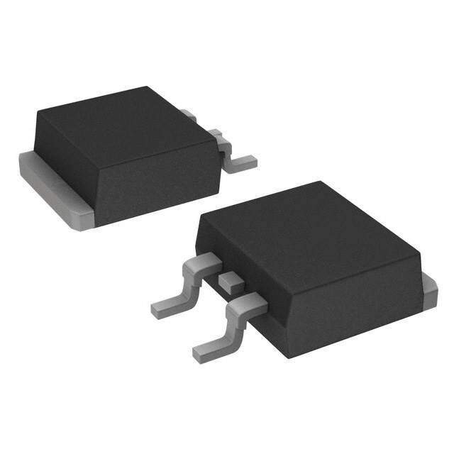
| 产品图片 |
|
| rohs | 符合RoHS无铅 / 符合限制有害物质指令(RoHS)规范要求 |
| 产品系列 | 电源管理 IC,线性稳压器,ON Semiconductor MC7915CD2TR4G- |
| 数据手册 | |
| 产品型号 | MC7915CD2TR4G |
| 产品种类 | |
| 供应商器件封装 | D2PAK |
| 其它名称 | MC7915CD2TR4GOSCT |
| 包装 | 剪切带 (CT) |
| 商标 | ON Semiconductor |
| 安装类型 | 表面贴装 |
| 安装风格 | SMD/SMT |
| 封装 | Reel |
| 封装/外壳 | TO-263-3,D²Pak(2 引线+接片),TO-263AB |
| 封装/箱体 | TO-263-3 (D2PAK) |
| 工作温度 | 0°C ~ 125°C |
| 工厂包装数量 | 800 |
| 最大工作温度 | + 125 C |
| 最大输入电压 | - 35 V |
| 最小工作温度 | 0 C |
| 最小输入电压 | - 35 V |
| 极性 | Negative |
| 标准包装 | 1 |
| 电压-跌落(典型值) | 1.3V @ 1A |
| 电压-输入 | 可下调至 -35V |
| 电压-输出 | -15V |
| 电流-输出 | 1A |
| 电流-限制(最小值) | - |
| 稳压器拓扑 | 负,固定式 |
| 稳压器数 | 1 |
| 系列 | MC7915 |
| 线路调整率 | 300 mV |
| 负载调节 | 300 mV |
| 输出电压 | - 15 V |
| 输出电流 | 1 A |
| 输出端数量 | 1 |
| 输出类型 | Fixed |


- 商务部:美国ITC正式对集成电路等产品启动337调查
- 曝三星4nm工艺存在良率问题 高通将骁龙8 Gen1或转产台积电
- 太阳诱电将投资9.5亿元在常州建新厂生产MLCC 预计2023年完工
- 英特尔发布欧洲新工厂建设计划 深化IDM 2.0 战略
- 台积电先进制程称霸业界 有大客户加持明年业绩稳了
- 达到5530亿美元!SIA预计今年全球半导体销售额将创下新高
- 英特尔拟将自动驾驶子公司Mobileye上市 估值或超500亿美元
- 三星加码芯片和SET,合并消费电子和移动部门,撤换高东真等 CEO
- 三星电子宣布重大人事变动 还合并消费电子和移动部门
- 海关总署:前11个月进口集成电路产品价值2.52万亿元 增长14.8%


PDF Datasheet 数据手册内容提取
MC7900 Series 1.0 A Negative Voltage Regulators The MC7900 series of fixed output negative voltage regulators are intended as complements to the popular MC7800 series devices. These negative regulators are available in the same seven−voltage options as the MC7800 devices. In addition, one extra voltage option http://onsemi.com commonly employed in MECL systems is also available in the negative MC7900 series. Available in fixed output voltage options from −5.0 V to −24 V, TO−220 these regulators employ current limiting, thermal shutdown, and T SUFFIX safe−area compensation − making them remarkably rugged under CASE 221AB most operating conditions. With adequate heatsinking they can deliver output currents in excess of 1.0 A. Heatsink surface • No External Components Required connected to Pin 2. 1 • Internal Thermal Overload Protection 2 3 • Internal Short Circuit Current Limiting Pin 1. Ground • Output Transistor Safe−Area Compensation 2. Input • 3. Output Available in 2% Voltage Tolerance (See Ordering Information) • Pb−Free Package May be Available. The G−Suffix Denotes a D2PAK Pb−Free Lead Finish D2T SUFFIX CASE 936 1 2 Gnd 3 2.4 k 14.7 k 2.0 k 2.0 k 8.0 k Heatsink surface (shown as terminal 4 in 25 case outline drawing) is connected to Pin 2. 3.6 k 1.0 k 4.0 k R1 0 k 1.2 k 12 k 1.0 k 4. 1.6 k STANDARD APPLICATION R2 Input MC79XX Output 10 k VO 0.33C (cid:2)inF* C1.O0* (cid:2)*F 20 pF 10 pF 10 k A common ground is required between the input 20 k 20 k 240 and the output voltages. The input voltage must 2.0 k 0.3 remain typically 2.0 V above more negative even 1.1 k during the high point of the input ripple voltage. 750 This device contains 26 active transistors. VI XX, These two digits of the type number indicate nominal voltage. ** Cin is required if regulator is located an Figure 1. Representative Schematic Diagram appreciable distance from power supply filter. ** CO improve stability and transient response. ORDERING INFORMATION See detailed ordering and shipping information in the package dimensions section on page 11 of this data sheet. DEVICE MARKING INFORMATION See general marking information in the device marking section on page 14 of this data sheet. © Semiconductor Components Industries, LLC, 2013 1 Publication Order Number: July, 2013 − Rev. 18 MC7900/D
MC7900 Series MAXIMUM RATINGS (TA = +25°C, unless otherwise noted.) Rating Symbol Value Unit Input Voltage (−5.0 V ≥ VO ≥ −18 V) VI −35 Vdc Input Voltage (24 V) −40 Power Dissipation Case 221A TA = +25°C PD Internally Limited W Thermal Resistance, Junction−to−Ambient (cid:3)JA 65 °C/W Thermal Resistance, Junction−to−Case (cid:3)JC 5.0 °C/W Case 936 (D2PAK) TA = +25°C PD Internally Limited W Thermal Resistance, Junction−to−Ambient (cid:3)JA 70 °C/W Thermal Resistance, Junction−to−Case (cid:3)JC 5.0 °C/W Storage Junction Temperature Range Tstg −65 to +150 °C Junction Temperature TJ +150 °C Stresses exceeding Maximum Ratings may damage the device. Maximum Ratings are stress ratings only. Functional operation above the Recommended Operating Conditions is not implied. Extended exposure to stresses above the Recommended Operating Conditions may affect device reliability. *This device series contains ESD protection and exceeds the following tests: Human Body Model 2000 V per MIL_STD_883, Method 3015 Machine Model Method 200 V MC7905B, MC7905C ELECTRICAL CHARACTERISTICS (VI = −10 V, IO = 500 mA, Tlow* < TJ < +125°C, unless otherwise noted.) Characteristics Symbol Min Typ Max Unit Output Voltage (TJ = +25°C) VO −4.8 −5.0 −5.2 Vdc Line Regulation (Note 1) Regline mV (TJ = +25°C, IO = 100 mA) −7.0 Vdc ≥ VI ≥ −25 Vdc − 7.0 50 −8.0 Vdc ≥ VI ≥ −12 Vdc − 2.0 25 (TJ = +25°C, IO = 500 mA) −7.0 Vdc ≥ VI ≥ −25 Vdc − 35 100 −8.0 Vdc ≥ VI ≥ −12 Vdc − 8.0 50 Load Regulation, TJ = +25°C (Note 1) Regload mV 5.0 mA ≤ IO ≤ 1.5 A − 11 100 250 mA ≤ IO ≤ 750 mA − 4.0 50 Output Voltage VO Vdc −7.0 Vdc ≥ VI ≥ −20 Vdc, 5.0 mA ≤ IO ≤ 1.0 A, P ≤ 15 W −(cid:2)4.75 − −(cid:2)5.25 Input Bias Current (TJ = +25°C) IIB − 4.3 8.0 mA Input Bias Current Change (cid:4)IIB mA −7.0 Vdc ≥ VI ≥ −25 Vdc − − 1.3 5.0 mA ≤ IO ≤ 1.5 A − − 0.5 Output Noise Voltage (TA = +25°C, 10 Hz ≤ f ≤ 100 kHz) Vn − 40 − (cid:2)V Ripple Rejection (IO = 20 mA, f = 120 Hz) RR − 70 − dB Dropout Voltage VI−VO Vdc IO = 1.0 A, TJ = +25°C − 1.3 − Average Temperature Coefficient of Output Voltage (cid:4)VO/(cid:4)T mV/°C IO = 5.0 mA, Tlow* ≤ TJ ≤ +125°C − −1.0 − 1. Load and line regulation are specified at constant junction temperature. Changes in VO due to heating effects must be taken into account separately. Pulse testing with low duty cycle is used. *Tlow = −40°C for MC7905B and Tlow = 0°C for MC7905C. http://onsemi.com 2
MC7900 Series MC7905AC ELECTRICAL CHARACTERISTICS (VI = −10 V, IO = 500 mA, 0°C < TJ < +125°C, unless otherwise noted.) Characteristics Symbol Min Typ Max Unit Output Voltage (TJ = +25°C) VO −4.9 −5.0 −5.1 Vdc Line Regulation (Note 2) Regline mV −8.0 Vdc ≥ VI ≥ −12 Vdc; IO = 1.0 A, TJ = +25°C − 2.0 25 −8.0 Vdc ≥ VI ≥ −12 Vdc; IO = 1.0 A − 7.0 50 −7.5 Vdc ≥ VI ≥ −25 Vdc; IO = 500 mA − 7.0 50 −7.0 Vdc ≥ VI ≥ −20 Vdc; IO = 1.0 A, TJ = +25°C − 6.0 50 Load Regulation (Note 2) Regload mV 5.0 mA ≤ IO ≤ 1.5 A, TJ = +25°C − 11 100 250 mA ≤ IO ≤ 750 mA − 4.0 50 5.0 mA ≤ IO ≤ 1.0 A − 9.0 100 Output Voltage VO Vdc −7.5 Vdc ≥ VI ≥ −20 Vdc, 5.0 mA ≤ IO ≤ 1.0 A, P ≤ 15 W −4.80 − −5.20 Input Bias Current IIB − 4.4 8.0 mA Input Bias Current Change (cid:4)IIB mA −7.5 Vdc ≥ VI ≥ −25 Vdc − − 1.3 5.0 mA ≤ IO ≤ 1.0 A − − 0.5 5.0 mA ≤ IO ≤ 1.5 A, TJ = +25°C − − 0.5 Output Noise Voltage (TA = +25°C, 10 Hz ≤ f ≤ 100 kHz) Vn − 40 − (cid:2)V Ripple Rejection (IO = mA, f = 120 Hz) RR − 70 − dB Dropout Voltage (IO = 1.0 A. TJ = +25°C) VI−VO − 1.3 − Vdc Average Temperature Coefficient of Output Voltage (cid:4)VO/(cid:4)T mV/°C IO = 5.0 A, 0°C ≤ TJ ≤ +125°C − −1.0 − MC7905.2C ELECTRICAL CHARACTERISTICS (VI = −10 V, IO = 500 mA, 0°C < TJ < +125°C, unless otherwise noted.) Characteristics Symbol Min Typ Max Unit Output Voltage (TJ = +25°C) VO −5.0 −5.2 −5.4 Vdc Line Regulation (Note 2) Regline mV (TJ = +25°C, IO = 100 mA) −7.2 Vdc ≥ VI ≥ −25 Vdc − 8.0 52 −8.0 Vdc ≥ VI ≥ −12 Vdc − 2.2 27 (TJ = +25°C, IO = 500 mA) −7.2 Vdc ≥ VI ≥ −25 Vdc − 37 105 −8.0 Vdc ≥ VI ≥ −12 Vdc − 8.5 52 Load Regulation, TJ = +25°C (Note 2) Regload mV 5.0 mA ≤ IO ≤ 1.5 A − 12 105 250 mA ≤ IO ≤ 750 mA − 4.5 52 Output Voltage VO Vdc −7.2 Vdc ≥ VI ≥ −20 Vdc, 5.0 mA ≤ IO ≤ 1.0 A, P ≤ 15 W −4.95 − −5.45 Input Bias Current (TJ = +25°C) IIB − 4.3 8.0 mA Input Bias Current Change (cid:4)IIB mA −7.2 Vdc ≥ VI ≥ −25 Vdc − − 1.3 5.0 mA ≤ IO ≤ 1.5 A − − 0.5 Output Noise Voltage (TA = +25°C, 10 Hz ≤ f ≤ 100 kHz) Vn − 42 − (cid:2)V Ripple Rejection (IO = 20 mA, f = 120 Hz) RR − 68 − dB Dropout Voltage (IO = 1.0 A, TJ = +25°C) VI−VO − 1.3 − Vdc Average Temperature Coefficient of Output Voltage (cid:4)VO/(cid:4)T mV/°C IO = 5.0 mA, 0°C ≤ TJ ≤ +125°C − −1.0 − 2. Load and line regulation are specified at constant junction temperature. Changes in VO due to heating effects must be taken into account separately. Pulse testing with low duty cycle is used. http://onsemi.com 3
MC7900 Series MC7906C ELECTRICAL CHARACTERISTICS (VI = −11 V, IO = 500 mA, 0°C < TJ < +125°C, unless otherwise noted.) Characteristics Symbol Min Typ Max Unit Output Voltage (TJ = +25°C) VO −5.75 −6.0 −6.25 Vdc Line Regulation (Note 3) Regline mV (TJ = +25°C, IO = 100 mA) −8.0 Vdc ≥ VI ≥ −25 Vdc − 9.0 60 −9.0 Vdc ≥ VI ≥ −13 Vdc − 3.0 30 (TJ = +25°C, IO = 500 mA) −8.0 Vdc ≥ VI ≥ −25 Vdc − 43 120 −9.0 Vdc ≥ VI ≥ −13 Vdc − 10 60 Load Regulation, TJ = +25°C (Note 3) Regload mV 5.0 mA ≤ IO ≤ 1.5 A − 13 120 250 mA ≤ IO ≤ 750 mA − 5.0 60 Output Voltage VO Vdc −8.0 Vdc ≥ VI ≥ −21 Vdc, 5.0 mA ≤ IO ≤ 1.0 A, P ≤ 15 W −5.7 − −6.3 Input Bias Current (TJ = +25°C) IIB − 4.3 8.0 mA Input Bias Current Change (cid:4)IIB mA −8.0 Vdc ≥ VI ≥ −25 Vdc − − 1.3 5.0 mA ≤ IO ≤ 1.5 A − − 0.5 Output Noise Voltage (TA = +25°C, 10 Hz ≤ f ≤ 100 kHz) Vn − 45 − (cid:2)V Ripple Rejection (IO = 20 mA, f = 120 Hz) RR − 65 − dB Dropout Voltage (IO = 1.0 A, TJ = +25°C) VI−VO − 1.3 − Vdc Average Temperature Coefficient of Output Voltage (cid:4)VO/(cid:4)T mV/°C IO = 5.0 A, 0°C ≤ TJ ≤ +125°C − −1.0 − MC7908C ELECTRICAL CHARACTERISTICS (VI = −14 V, IO = 500 mA, 0°C < TJ < +125°C, unless otherwise noted.) Characteristics Symbol Min Typ Max Unit Output Voltage (TJ = +25°C) VO −7.7 −8.0 −8.3 Vdc Line Regulation (Note 3) Regline mV (TJ = +25°C, IO = 100 mA) −10.5 Vdc ≥ VI ≥ −25 Vdc − 12 80 −11 Vdc ≥ VI ≥ −17 Vdc − 5.0 40 (TJ = +25°C, IO = 500 mA) −10.5 Vdc ≥ VI ≥ −25 Vdc − 50 160 −11 Vdc ≥ VI ≥ −17 Vdc − 22 80 Load Regulation, TJ = +25°C (Note 3) Regload mV 5.0 mA ≤ IO ≤ 1.5 A − 26 160 250 mA ≤ IO ≤ 750 mA − 9.0 80 Output Voltage VO Vdc −10.5 Vdc ≥ VI ≥ −23 Vdc, 5.0 mA ≤ IO ≤ 1.0 A, P ≤ 15 W −7.6 − −8.4 Input Bias Current (TJ = +25°C) IIB − 4.3 8.0 mA Input Bias Current Change (cid:4)IIB mA −10.5 Vdc ≥ VI ≥ −25 Vdc − − 1.0 5.0 mA ≤ IO ≤ 1.5 A − − 0.5 Output Noise Voltage (TA = +25°C, 10 Hz ≤ f ≤ 100 kHz) Vn − 52 − (cid:2)V Ripple Rejection (IO = 20 mA, f = 120 Hz) RR − 62 − dB Dropout Voltage (IO = 1.0 A, TJ = +25°C) VI−VO − 1.3 − Vdc Average Temperature Coefficient of Output Voltage (cid:4)VO/(cid:4)T mV/°C IO = 5.0 mA, 0°C ≤ TJ ≤ +125°C − −1.0 − 3. Load and line regulation are specified at constant junction temperature. Changes in VO due to heating effects must be taken into account separately. Pulse testing with low duty cycle is used. http://onsemi.com 4
MC7900 Series MC7912B, MC7912C ELECTRICAL CHARACTERISTICS (VI = −19 V, IO = 500 mA, Tlow* < TJ < +125°C, unless otherwise noted.) Characteristics Symbol Min Typ Max Unit Output Voltage (TJ = +25°C) VO −11.5 −12 −12.5 Vdc Line Regulation (Note 4) Regline mV (TJ = +25°C, IO = 100 mA) −14.5 Vdc ≥ VI ≥ −30 Vdc − 13 120 −16 Vdc ≥ VI ≥ −22 Vdc − 6.0 60 (TJ = +25°C, IO = 500 mA) −14.5 Vdc ≥ VI ≥ −30 Vdc − 55 240 −16 Vdc ≥ VI ≥ −22 Vdc − 24 120 Load Regulation, TJ = +25°C (Note 4) Regload mV 5.0 mA ≤ IO ≤ 1.5 A − 46 240 250 mA ≤ IO ≤ 750 mA − 17 120 Output Voltage VO Vdc −14.5 Vdc ≥ VI ≥ −27 Vdc, 5.0 mA ≤ IO ≤ 1.0 A, P ≤ 15 W −11.4 − −12.6 Input Bias Current (TJ = +25°C) IIB − 4.4 8.0 mA Input Bias Current Change (cid:4)IIB mA −14.5 Vdc ≥ VI ≥ −30 Vdc − − 1.0 5.0 mA ≤ IO ≤ 1.5 A − − 0.5 Output Noise Voltage (TA = +25°C, 10 Hz ≤ f ≤ 100 kHz) Vn − 75 − (cid:2)V Ripple Rejection (IO = 20 mA, f = 120 Hz) RR − 61 − dB Dropout Voltage (IO = 1.0 A, TJ = +25°C) VI−VO − 1.3 − Vdc Average Temperature Coefficient of Output Voltage (cid:4)VO/(cid:4)T mV/°C IO = 5.0 mA, Tlow* ≤ TJ ≤ +125°C − −1.0 − MC7912AC ELECTRICAL CHARACTERISTICS (VI = −19 V, IO = 500 mA, Tlow* < TJ < +125°C, unless otherwise noted.) Characteristics Symbol Min Typ Max Unit Output Voltage (TJ = +25°C) VO −11.75 −12 −12.25 Vdc Line Regulation (Note 4) Regline mV −16 Vdc ≥ VI ≥ −22 Vdc; IO = 1.0 A, TJ = +25°C − 6.0 60 −16 Vdc ≥ VI ≥ −22 Vdc; IO = 1.0 A − 24 120 −14.8 Vdc ≥ VI ≥ −30 Vdc; IO = 500 mA − 24 120 −14.5 Vdc ≥ VI ≥ −27 Vdc; IO = 1.0 A, TJ = +25°C − 13 120 Load Regulation (Note 4) Regload mV 5.0 mA ≤ IO ≤ 1.5 A, TJ = +25°C − 46 150 250 mA ≤ IO ≤ 750 mA − 17 75 5.0 mA ≤ IO ≤ 1.0 A − 35 150 Output Voltage VO Vdc −14.8 Vdc ≥ VI ≥ −27 Vdc, 5.0 mA ≤ IO ≤ 1.0 A, P ≤ 15 W −11.5 − −12.5 Input Bias Current IIB − 4.4 8.0 mA Input Bias Current Change (cid:4)IIB mA −15 Vdc ≥ VI ≥ −30 Vdc − − 0.8 5.0 mA ≤ IO ≤ 1.0 A − − 0.5 5.0 mA ≤ IO ≤ 1.5 A, TJ = +25°C − − 0.5 Output Noise Voltage (TA = +25°C, 10 Hz ≤ f ≤ 100 kHz) Vn − 75 − (cid:2)V Ripple Rejection (IO = 20 mA, f = 120 Hz) RR − 61 − dB Dropout Voltage (IO = 1.0 A, TJ = +25°C) VI−VO − 1.3 − Vdc Average Temperature Coefficient of Output Voltage (cid:4)VO/(cid:4)T mV/°C IO = 5.0 A, Tlow* ≤ TJ ≤ +125°C − −1.0 − 4. Load and line regulation are specified at constant junction temperature. Changes in VO due to heating effects must be taken into account separately. Pulse testing with low duty cycle is used. *Tlow = −40°C for MC7912B and Tlow = 0°C for MC7912C. http://onsemi.com 5
MC7900 Series MC7915B, MC7915C ELECTRICAL CHARACTERISTICS (VI = −23 V, IO = 500 mA, Tlow* < TJ < +125°C, unless otherwise noted.) Characteristics Symbol Min Typ Max Unit Output Voltage (TJ = +25°C) VO −14.4 −15 −15.6 Vdc Line Regulation (Note 5) Regline mV (TJ = +25°C, IO = 100 mA) −17.5 Vdc ≥ VI ≥ −30 Vdc − 14 150 −20 Vdc ≥ VI ≥ −26 Vdc − 6.0 75 (TJ = +25°C, IO = 500 mA) −17.5 Vdc ≥ VI ≥ −30 Vdc − 57 300 −20 Vdc ≥ VI ≥ −26 Vdc − 27 150 Load Regulation, TJ = +25°C (Note 5) Regload mV 5.0 mA ≤ IO ≤ 1.5 A − 68 300 250 mA ≤ IO ≤ 750 mA − 25 150 Output Voltage VO Vdc −17.5 Vdc ≥ VI ≥ −30 Vdc, 5.0 mA ≤ IO ≤ 1.0 A, P ≤ 15 W −14.25 − −15.75 Input Bias Current (TJ = +25°C) IIB − 4.4 8.0 mA Input Bias Current Change (cid:4)IIB mA −17.5 Vdc ≥ VI ≥ −30 Vdc − − 1.0 5.0 mA ≤ IO ≤ 1.5 A − − 0.5 Output Noise Voltage (TA = +25°C, 10 Hz ≤ f ≤ 100 kHz) Vn − 90 − (cid:2)V Ripple Rejection (IO = 20 mA, f = 120 Hz) RR − 60 − dB Dropout Voltage (IO = 1.0 A, TJ = +25°C) VI−VO − 1.3 − Vdc Average Temperature Coefficient of Output Voltage (cid:4)VO/(cid:4)T mV/°C IO = 5.0 A, Tlow* ≤ TJ ≤ +125°C − −1.0 − MC7915AC ELECTRICAL CHARACTERISTICS (VI = −23 V, IO = 500 mA, Tlow* < TJ < +125°C, unless otherwise noted.) Characteristics Symbol Min Typ Max Unit Output Voltage (TJ = +25°C) VO −14.7 −15 −15.3 Vdc Line Regulation (Note 5) Regline mV −20 Vdc ≥ VI ≥ −26 Vdc, IO = 1.0 A, TJ = +25°C − 27 75 −20 Vdc ≥ VI ≥ −26 Vdc, IO = 1.0 A, − 57 150 −17.9 Vdc ≥ VI ≥ −30 Vdc, IO = 500 mA − 57 150 −17.5 Vdc ≥ VI ≥ −30 Vdc, IO = 1.0 A, TJ = +25°C − 57 150 Load Regulation (Note 5) Regload mV 5.0 mA ≤ IO ≤ 1.5 A, TJ = +25°C − 68 150 250 mA ≤ IO ≤ 750 mA − 25 75 5.0 mA ≤ IO ≤ 1.0 A − 40 150 Output Voltage VO Vdc −17.9 Vdc ≥ VI ≥ −30 Vdc, 5.0 mA ≤ IO ≤ 1.0 A, P ≤ 15 W −14.4 − −15.6 Input Bias Current IIB − 4.4 8.0 mA Input Bias Current Change (cid:4)IIB mA −17.5 Vdc ≥ VI ≥ −30 Vdc − − 0.8 5.0 mA ≤ IO ≤ 1.0 A − − 0.5 5.0 mA ≤ IO ≤ 1.5 A, TJ = +25°C − − 0.5 Output Noise Voltage (TA = +25°C, 10 Hz ≤ f ≤ 100 kHz) Vn − 90 − (cid:2)V Ripple Rejection (IO = 20 mA, f = 120 Hz) RR − 60 − dB Dropout Voltage (IO = 1.0 A, TJ = +25°C) VI−VO − 1.3 − Vdc Average Temperature Coefficient of Output Voltage (cid:4)VO/(cid:4)T mV/°C IO = 5.0 mA, Tlow* ≤ TJ ≤ +125°C − −1.0 − 5. Load and line regulation are specified at constant junction temperature. Changes in VO due to heating effects must be taken into account separately. Pulse testing with low duty cycle is used. *Tlow = −40°C for MC7915B and Tlow = 0°C for MC7915C. http://onsemi.com 6
MC7900 Series MC7918C ELECTRICAL CHARACTERISTICS (VI = −27 V, IO = 500 mA, 0°C < TJ < +125°C, unless otherwise noted.) Characteristics Symbol Min Typ Max Unit Output Voltage (TJ = +25°C) VO −17.3 −18 −18.7 Vdc Line Regulation (Note 6) Regline mV (TJ = +25°C, IO = 100 mA) −21 Vdc ≥ VI ≥ −33 Vdc − 25 180 −24 Vdc ≥ VI ≥ −30 Vdc − 10 90 (TJ = +25°C, IO = 500 mA) −21 Vdc ≥ VI ≥ −33 Vdc − 90 360 −24 Vdc ≥ VI ≥ −30 Vdc − 50 180 Load Regulation, TJ = +25°C (Note 6) Regload mV 5.0 mA ≤ IO ≤ 1.5 A − 110 360 250 mA ≤ IO ≤ 750 mA − 55 180 Output Voltage VO Vdc −21 Vdc ≥ VI ≥ −33 Vdc, 5.0 mA ≤ IO ≤ 1.0 A, P ≤ 15 W −17.1 − −18.9 Input Bias Current (TJ = +25°C) IIB − 4.5 8.0 mA Input Bias Current Change (cid:4)IIB mA −21 Vdc ≥ VI ≥ −33 Vdc − − 1.0 5.0 mA ≤ IO ≤ 1.5 A − − 0.5 Output Noise Voltage (TA = +25°C, 10 Hz ≤ f ≤ 100 kHz) Vn − 110 − (cid:2)V Ripple Rejection (IO = 20 mA, f = 120 Hz) RR − 59 − dB Dropout Voltage (IO = 1.0 A, TJ = +25°C) VI−VO − 1.3 − Vdc Average Temperature Coefficient of Output Voltage (cid:4)VO/(cid:4)T mV/°C IO = 5.0 mA, 0°C ≤ TJ ≤ +125°C − −1.0 − MC7924B, MC7924C ELECTRICAL CHARACTERISTICS (VI = −33 V, IO = 500 mA, Tlow* < TJ < +125°C, unless otherwise noted.) Characteristics Symbol Min Typ Max Unit Output Voltage (TJ = +25°C) VO −23 −24 −25 Vdc Line Regulation (Note 6) Regline mV (TJ = +25°C, IO = 100 mA) −27 Vdc ≥ VI ≥ −38 Vdc − 31 240 −30 Vdc ≥ VI ≥ −36 Vdc − 14 120 (TJ = +25°C, IO = 500 mA) −27 Vdc ≥ VI ≥ −38 Vdc − 118 470 −30 Vdc ≥ VI ≥ −36 Vdc − 70 240 Load Regulation, TJ = +25°C (Note 6) Regload mV 5.0 mA ≤ IO ≤ 1.5 A − 150 480 250 mA ≤ IO ≤ 750 mA − 85 240 Output Voltage VO Vdc −27 Vdc ≥ VI ≥ −38 Vdc, 5.0 mA ≤ IO ≤ 1.0 A, P ≤ 15 W −22.8 − −25.2 Input Bias Current (TJ = +25°C) IIB − 4.6 8.0 mA Input Bias Current Change (cid:4)IIB mA −27 Vdc ≥ VI ≥ −38 Vdc − − 1.0 5.0 mA ≤ IO ≤ 1.5 A − − 0.5 Output Noise Voltage (TA = +25°C, 10 Hz ≤ f ≤ 100 kHz) Vn − 170 − (cid:2)V Ripple Rejection (IO = 20 mA, f = 120 Hz) RR − 56 − dB Dropout Voltage (IO = 1.0 A, TJ = +25°C) VI−VO − 1.3 − Vdc Average Temperature Coefficient of Output Voltage (cid:4)VO/(cid:4)T mV/°C IO = 5.0 mA, Tlow* ≤ TJ ≤ +125°C − −1.0 − 6. Load and line regulation are specified at constant junction temperature. Changes in VO due to heating effects must be taken into account separately. Pulse testing with low duty cycle is used. *Tlow = −40°C for MC7924B and Tlow = 0°C for MC7924C. http://onsemi.com 7
MC7900 Series 20 2.5 Infinite Heatsink 10 W) (cid:3)HS = 5°C/W A) 2.0 ON ( 54..00 (cid:3)HS = 15°C/W ENT ( TJ = +25°C TI 3.0 R A R 1.5 P 2.0 U SI C DIS No Heatsink UT WER 10..05 OUTP 1.0 PO 0.4 , O , PD 00..32 (cid:3)(cid:3)JJCA == 655°°CC/W/W I 0.5 0.1 PD(max) = 15W 0 25 50 75 100 125 150 0 3.0 6.0 9.0 12 15 18 21 24 27 30 TA, AMBIENT TEMPERATURE (°C) |VI -VO| INPUT-OUTPUT VOLTAGE DIFFERENTIAL (V) Figure 2. Worst Case Power Dissipation as a Figure 3. Peak Output Current as a Function Function of Ambient Temperature of Input−Output Differential Voltage 100 80 Vin = -11 V ECTION (dB) 8600 VIOO = = 2 -0(cid:2)6 m.0A V CTION (dB) 70 fI(cid:4)O =V =1in 22 =00 1Hm.z0A V(RMS) J E RE EJ 60 PLE 40 LE R P P RR, RI 20 R, RIP 50 R 0 40 10 100 1.0 k 10 k 100 k 2.0 4.0 6.0 8.0 10 12 14 16 18 20 22 f, FREQUENCY (Hz) VO, OUTPUT VOLTAGE (V) Figure 4. Ripple Rejection as a Figure 5. Ripple Rejection as a Function Function of Frequency of Output Voltage 6.26 5.2 GE (-V)6.22 ENT (mA)5.0 OLTA6.18 URR4.8 V C T S U A , OUTPVO66..1140 IVVOiDn = == 2 --0(cid:2)16 m1.0 AV V , INPUT BIB44..64 VVIOiOn = == 2 --01(cid:2)6 m1.0 AV V II 6.06 4.2 -25 0 25 50 75 100 125 150 175 0 25 50 75 100 125 TJ, JUNCTION TEMPERATURE (°C) TJ, JUNCTION TEMPERATURE (°C) Figure 6. Output Voltage as a Function Figure 7. Quiescent Current as a of Junction Temperature Function of Temperature http://onsemi.com 8
MC7900 Series APPLICATIONS INFORMATION Design Considerations -10 V 0.56 -(cid:2)5.0 V The MC7900 Series of fixed voltage regulators are Input Output 2N3055* 0.56 designed with Thermal overload Protection that shuts down or Equiv the circuit when subjected to an excessive power overload 0.56 condition. Internal Short Circuit Protection that limits the MJE200* maximum current the circuit will pass, and Output Transistor or Equiv MC7905* Safe−Area Compensation that reduces the output short circuit current as the voltage across the pass transistor is increased. In many low current applications, compensation 10 (cid:2)F 5.6 1.0 (cid:2)F 1.0 (cid:2)F capacitors are not required. However, it is recommended + + + Gnd Gnd that the regulator input be bypassed with a capacitor if the *Mounted on heatsink. regulator is connected to the power supply filter with long Figure 9. Current Boost Regulator wire lengths, or if the output load capacitance is large. An (−5.0 V @ 4.0 A, with 5.0 A Current Limiting) input bypass capacitor should be selected to provide good When a boost transistor is used, short circuit currents are high−frequency characteristics to insure stable operation equal to the sum of the series pass and regulator limits, which under all load conditions. A 0.33 (cid:2)F or larger tantalum, are measured at 3.2 A and 1.8 A respectively in this case. mylar, or other capacitor having low internal impedance at Series pass limiting is approximately equal to 0.6 V/R . SC high frequencies should be chosen. The capacitor chosen Operation beyond this point to the peak current capability of should have an equivalent series resistance of less than the MC7905C is possible if the regulator is mounted on a 0.7(cid:5)(cid:6). The bypass capacitor should be mounted with the heatsink; otherwise thermal shutdown will occur when the shortest possible leads directly across the regulators input additional load current is picked up by the regulator. terminals. Normally good construction techniques should be 1N4001G or Equiv used to minimize ground loops and lead resistance drops since the regulator has no external sense lead. Bypassing the +20 V +15 V output is also recommended. Input Output -20 V 10 IO = 200 mA MC7815 Clamp diode Input MC7905 + + R - 0.33 (cid:2)F 1.0 (cid:2)F 1.0 (cid:2)F 1N4001G VO ≤ 10 V or Equiv Gnd Gnd + + 1.0 (cid:2)F 1.0 (cid:2)F 1.0 (cid:2)F 1.0 (cid:2)F 1N4001G + + or Equiv Gnd Gnd MC7915 Figure 8. Current Regulator -(cid:2)20 V -15 V Input Output The MC7905, −5.0 V regulator can be used as a constant current source when connected as above. The output current 1N4001G or Equiv is the sum of resistor R current and quiescent bias current as Figure 10. Operational Amplifier Supply follows: The MC7815 and MC7915 positive and negative I (cid:2)5.0V(cid:3)I regulators may be connected as shown to obtain a dual O R B power supply for operational amplifiers. A clamp diode The quiescent current for this regulator is typically 4.3 should be used at the output of the MC7815 to prevent mA. The 5.0V regulator was chosen to minimize dissipation potential latch−up problems whenever the output of the and to allow the output voltage to operate to within 6.0 V positive regulator (MC7815) is drawn below ground with an below the input voltage. output current greater than 200 mA. http://onsemi.com 9
MC7900 Series Protection Diodes Diode D2 prevents output capacitor from discharging thru When external capacitors are used with MC7900 series the MC7915 during an input short circuit or fast switch off regulator it is sometimes necessary to add protection diodes of power supply. to prevent the capacitors from discharging through low Gnd Gnd current points into the regulator or from output polarity + + reversals. Generally, no protection diode is required for 1.0 (cid:2)F 1.0 (cid:2)F D1 MBRS140 or Equiv values of output capacitance less then 10(cid:2)F. Figure 11 shows MC7915 the MC7915 with the recommended protection diodes. -(cid:2)20 V -15 V • Input Output Opposite Polarity Protection Diode D1 protects the regulator from output polarity D2MBRS140 reversals during startup, power off and short-circuit or Equiv operation. Figure 11. Protection Diodes • Reverse-bias Protection DEFINITIONS Line Regulation − The change in output voltage for a Input Bias Current − That part of the input current that change in the input voltage. The measurement is made under is not delivered to the load. conditions of low dissipation or by using pulse techniques Output Noise Voltage − The rms AC voltage at the such that the average chip temperature is not significantly output, with constant load and no input ripple, measured affected. over a specified frequency range. Load Regulation − The change in output voltage for a Long Term Stability − Output voltage stability under change in load current at constant chip temperature. accelerated life test conditions with the maximum rated Maximum Power Dissipation − The maximum total voltage listed in the devices’ electrical characteristics and device dissipation for which the regulator will operate maximum power dissipation. within specifications. 80 3.5 W) PD(max) for TA = +50°C N ( E O , THERMAL RESISTANCθJA°JUNCTION‐TO‐AIR ( C/W) 45670000 VMFeroreuteicn aAtelildry MSiizneim Puamd L2.ÎÎÎÎ0 oz.ÎÎÎÎ CLoppÎÎÎÎer 1223....5050 AXIMUM POWER DISSIPATI R M R(cid:3)JA , D P 30 1.0 0 5.0 10 15 20 25 30 L, LENGTH OF COPPER (mm) Figure 12. D2PAK Thermal Resistance and Maximum Power Dissipation versus P.C.B. Copper Length http://onsemi.com 10
MC7900 Series ORDERING INFORMATION Nominal Output Voltage Operating Device Output Voltage Tolerance Package Temperature Range Shipping† MC7905ACD2T −5.0 V 2% D2PAK TJ = 0°C to +125°C 50 Units/Rail MC7905ACD2TG D2PAK 50 Units/Rail (Pb−Free) MC7905ACD2TR4 D2PAK 800 Tape & Reel MC7905ACD2TR4G D2PAK 800 Tape & Reel (Pb−Free) MC7905ACT TO−220 50 Units/Rail MC7905ACTG TO−220 50 Units/Rail (Pb−Free) MC7905BD2T 4% D2PAK TJ = −40°C to +125°C 50 Units/Rail MC7905BD2TG D2PAK 50 Units/Rail (Pb−Free) MC7905BD2TR4 D2PAK 800 Tape & Reel MC7905BD2TR4G D2PAK 800 Tape & Reel (Pb−Free) MC7905BT TO−220 50 Units/Rail MC7905BTG TO−220 50 Units/Rail (Pb−Free) MC7905CD2T D2PAK TJ = 0°C to +125°C 50 Units/Rail MC7905CD2TG D2PAK 50 Units/Rail (Pb−Free) MC7905CD2TR4 D2PAK 800 Tape & Reel MC7905CD2TR4G D2PAK 800 Tape & Reel (Pb−Free) MC7905CT TO−220 50 Units/Rail MC7905CTG TO−220 50 Units/Rail (Pb−Free) MC7905.2CT −5.2 V 4% TO−220 TJ = 0°C to +125°C 50 Units/Rail MC7905.2CTG TO−220 50 Units/Rail (Pb−Free) MC7906CD2T −6.0 V 4% D2PAK TJ = 0°C to +125°C 50 Units/Rail MC7906CD2TG D2PAK 50 Units/Rail (Pb−Free) MC7906CT TO−220 50 Units/Rail MC7906CTG TO−220 50 Units/Rail (Pb−Free) MC7908ACT −8.0 V 2% TO−220 TJ = 0°C to +125°C 50 Units/Rail MC7908ACTG TO−220 50 Units/Rail (Pb−Free) MC7908CD2T 4% D2PAK 50 Units/Rail MC7908CD2TG D2PAK 50 Units/Rail (Pb−Free) MC7908CD2TR4 D2PAK 800 Tape & Reel MC7908CD2TR4G D2PAK 800 Tape & Reel (Pb−Free) MC7908CT TO−220 50 Units/Rail MC7908CTG TO−220 50 Units/Rail (Pb−Free) http://onsemi.com 11
MC7900 Series Nominal Output Voltage Operating Device Output Voltage Tolerance Package Temperature Range Shipping† MC7912ACD2T −12 V 2% D2PAK TJ = 0°C to +125°C 50 Units/Rail MC7912ACD2TG D2PAK 50 Units/Rail (Pb−Free) MC7912ACD2TR4 D2PAK 800 Tape & Reel MC7912ACD2TR4G D2PAK 800 Tape & Reel (Pb−Free) MC7912ACT TO−220 50 Units/Rail MC7912ACTG TO−220 50 Units/Rail (Pb−Free) MC7912BD2T 4% D2PAK TJ = −40°C to +125°C 50 Units/Rail MC7912BD2TG D2PAK 50 Units/Rail (Pb−Free) MC7912BD2TR4 D2PAK 800 Tape & Reel MC7912BD2TR4G D2PAK 800 Tape & Reel (Pb−Free) MC7912BT TO−220 50 Units/Rail MC7912BTG TO−220 50 Units/Rail (Pb−Free) MC7912CD2T D2PAK TJ = 0°C to +125°C 50 Units/Rail MC7912CD2TG D2PAK 50 Units/Rail (Pb−Free) MC7912CD2TR4 D2PAK 800 Tape & Reel MC7912CD2TR4G D2PAK 800 Tape & Reel (Pb−Free) MC7912CT TO−220 50 Units/Rail MC7912CTG TO−220 50 Units/Rail (Pb−Free) http://onsemi.com 12
MC7900 Series Nominal Output Voltage Operating Device Output Voltage Tolerance Package Temperature Range Shipping† MC7915ACD2T − 15 V 2% D2PAK TJ = 0°C to +125°C 50 Units/Rail MC7915ACD2TG D2PAK 50 Units/Rail (Pb−Free) MC7915ACT TO−220 50 Units/Rail MC7915ACTG TO−220 50 Units/Rail (Pb−Free) MC7915BD2T 4% D2PAK TJ = −40°C to +125°C 50 Units/Rail MC7915BD2TG D2PAK 50 Units/Rail (Pb−Free) MC7915BT TO−220 50 Units/Rail MC7915BTG TO−220 50 Units/Rail (Pb−Free) MC7915BD2TR4G D2PAK 800 Tape & Reel (Pb−Free) MC7915CD2T D2PAK TJ = 0°C to +125°C 50 Units/Rail MC7915CD2TG D2PAK 50 Units/Rail (Pb−Free) MC7915CD2TR4 D2PAK 800 Tape & Reel MC7915CD2TR4G D2PAK 800 Tape & Reel (Pb−Free) MC7915CT TO−220 50 Units/Rail MC7915CTG TO−220 50 Units/Rail (Pb−Free) MC7918CT − 18 V 4% TO−220 TJ = 0°C to +125°C 50 Units/Rail MC7918CTG TO−220 50 Units/Rail (Pb−Free) MC7924BT − 24 V 4% TO−220 TJ = −40°C to +125°C 50 Units/Rail MC7924BTG TO−220 50 Units/Rail (Pb−Free) MC7924CD2T D2PAK TJ = 0°C to +125°C 50 Units/Rail MC7924CD2TG D2PAK 50 Units/Rail (Pb−Free) MC7924CT TO−220 50 Units/Rail MC7924CTG TO−220 50 Units/Rail (Pb−Free) †For information on tape and reel specifications, including part orientation and tape sizes, please refer to our Tape and Reel Packaging Specifications Brochure, BRD8011/D. http://onsemi.com 13
MC7900 Series MARKING DIAGRAMS TO−220 T SUFFIX CASE 221AB MC MC MC MC 79xxACT 7905.2CT 79xxBT 79xxCT AWLYWWG AWLYWWG AWLYWWG AWLYWWG 1 2 3 1 2 3 1 2 3 1 2 3 D2PAK D2T SUFFIX CASE 936 MC MC MC 79xxACD2T 79xxBD2T 79xxCD2T AWLYWWG AWLYWWG AWLYWWG 2 2 2 1 3 1 3 1 3 xx = Nominal Voltage A = Assembly Location WL = Wafer Lot Y = Year WW= Work Week G = Pb−Free Device http://onsemi.com 14
MC7900 Series PACKAGE DIMENSIONS D2PAK D2T SUFFIX CASE 936−03 ISSUE D NOTES: T T (cid:4)(cid:5)1. DIMENSIONING AND TOLERANCING PER ANSI TERMINAL 4 Y14.5M, 1982. K A OCHPATIMOFNCEARL ED U OCHPATIMOFNCEARL ES (cid:4)(cid:4)(cid:5)(cid:5)23..DIMCTEAONBNS CTIORONONSLT LOAINU AGRN DOD IPKMT.EIONNSAIOLN W: IINTHCIHNES. (cid:4)(cid:5)4. DIMENSIONS U AND V ESTABLISH A MINIMUM S MOUNTING SURFACE FOR TERMINAL 4. V (cid:4)(cid:5)5. DIMENSIONS A AND B DO NOT INCLUDE B MOLD FLASH OR GATE PROTRUSIONS. MOLD H DETAIL C DETAIL C FLASH AND GATE PROTRUSIONS NOT TO 1 2 3 EXCEED 0.025 (0.635) MAXIMUM. (cid:4)(cid:5)6. SINGLE GAUGE DESIGN WILL BE SHIPPED AFTER FPCN EXPIRATION IN OCTOBER 2011. J INCHES MILLIMETERS F SIDE VIEW BOTTOM VIEW SIDE VIEW DIM MIN MAX MIN MAX G DUAL GAUGE SINGLE GAUGE A 0.386 0.403 9.804 10.236 2XD CONSTRUCTION CONSTRUCTION BC 00..315760 00..316880 94..034128 94..354772 0.010 (0.254) M T D 0.026 0.036 0.660 0.914 TOP VIEW ED 0.045 0.055 1.143 1.397 ES 0.018 0.026 0.457 0.660 F 0.051 REF 1.295 REF G 0.100 BSC 2.540 BSC H 0.539 0.579 13.691 14.707 N T J 0.125 MAX 3.175 MAX M K 0.050 REF 1.270 REF L 0.000 0.010 0.000 0.254 M 0.088 0.102 2.235 2.591 SEATING N 0.018 0.026 0.457 0.660 P L PLANE P 0.058 0.078 1.473 1.981 R 5 (cid:2) REF 5 (cid:2) REF R DETAIL C BOTTOM VIEW S 0.116 REF 2.946 REF OPTIONAL CONSTRUCTIONS U 0.200 MIN 5.080 MIN V 0.250 MIN 6.350 MIN SOLDERING FOOTPRINT* 10.490 8.380 16.155 2X 3.504 2X1.016 5.080 PITCH DIMENSIONS: MILLIMETERS *For additional information on our Pb−Free strategy and soldering details, please download the ON Semiconductor Soldering and Mounting Techniques Reference Manual, SOLDERRM/D. http://onsemi.com 15
MC7900 Series PACKAGE DIMENSIONS TO−220, SINGLE GAUGE T SUFFIX CASE 221AB ISSUE A NOTES: 1. DIMENSIONING AND TOLERANCING PER ANSI Y14.5M, 1982. −T− SPELAATNIENG 23.. CDOIMNETNRSOIOLLNI NZG D DEFIMINEENSS IAO ZNO: INNEC WHEHSE.RE ALL BODY AND B F C LEAD IRREGULARITIES ARE ALLOWED. 4. PRODUCT SHIPPED PRIOR TO 2008 HAD DIMENSIONS T S S = 0.045 - 0.055 INCHES (1.143 - 1.397 MM) 4 INCHES MILLIMETERS DIM MIN MAX MIN MAX A 0.570 0.620 14.48 15.75 Q A B 0.380 0.405 9.66 10.28 C 0.160 0.190 4.07 4.82 1 2 3 U D 0.025 0.035 0.64 0.88 H F 0.142 0.147 3.61 3.73 G 0.095 0.105 2.42 2.66 K H 0.110 0.155 2.80 3.93 Z J 0.018 0.025 0.46 0.64 K 0.500 0.562 12.70 14.27 L 0.045 0.060 1.15 1.52 N 0.190 0.210 4.83 5.33 L R Q 0.100 0.120 2.54 3.04 R 0.080 0.110 2.04 2.79 V J S 0.020 0.024 0.508 0.61 G T 0.235 0.255 5.97 6.47 U 0.000 0.050 0.00 1.27 D V 0.045 --- 1.15 --- N Z --- 0.080 --- 2.04 ON Semiconductor and are registered trademarks of Semiconductor Components Industries, LLC (SCILLC). SCILLC owns the rights to a number of patents, trademarks, copyrights, trade secrets, and other intellectual property. A listing of SCILLC’s product/patent coverage may be accessed at www.onsemi.com/site/pdf/Patent−Marking.pdf. SCILLC reserves the right to make changes without further notice to any products herein. SCILLC makes no warranty, representation or guarantee regarding the suitability of its products for any particular purpose, nor does SCILLC assume any liability arising out of the application or use of any product or circuit, and specifically disclaims any and all liability, including without limitation special, consequential or incidental damages. “Typical” parameters which may be provided in SCILLC data sheets and/or specifications can and do vary in different applications and actual performance may vary over time. All operating parameters, including “Typicals” must be validated for each customer application by customer’s technical experts. SCILLC does not convey any license under its patent rights nor the rights of others. SCILLC products are not designed, intended, or authorized for use as components in systems intended for surgical implant into the body, or other applications intended to support or sustain life, or for any other application in which the failure of the SCILLC product could create a situation where personal injury or death may occur. Should Buyer purchase or use SCILLC products for any such unintended or unauthorized application, Buyer shall indemnify and hold SCILLC and its officers, employees, subsidiaries, affiliates, and distributors harmless against all claims, costs, damages, and expenses, and reasonable attorney fees arising out of, directly or indirectly, any claim of personal injury or death associated with such unintended or unauthorized use, even if such claim alleges that SCILLC was negligent regarding the design or manufacture of the part. SCILLC is an Equal Opportunity/Affirmative Action Employer. This literature is subject to all applicable copyright laws and is not for resale in any manner. PUBLICATION ORDERING INFORMATION LITERATURE FULFILLMENT: N. American Technical Support: 800−282−9855 Toll Free ON Semiconductor Website: www.onsemi.com Literature Distribution Center for ON Semiconductor USA/Canada P.O. Box 5163, Denver, Colorado 80217 USA Europe, Middle East and Africa Technical Support: Order Literature: http://www.onsemi.com/orderlit Phone: 303−675−2175 or 800−344−3860 Toll Free USA/Canada Phone: 421 33 790 2910 Fax: 303−675−2176 or 800−344−3867 Toll Free USA/Canada Japan Customer Focus Center For additional information, please contact your local Email: orderlit@onsemi.com Phone: 81−3−5817−1050 Sales Representative http://onsemi.com MC7900/D 16
Mouser Electronics Authorized Distributor Click to View Pricing, Inventory, Delivery & Lifecycle Information: O N Semiconductor: MC7905.2CTG MC7905ACD2TG MC7905ACD2TR4G MC7905ACTG MC7905BD2TG MC7905BD2TR4G MC7905BTG MC7905CD2TG MC7905CD2TR4G MC7905CTG MC7906CD2TG MC7906CTG MC7908ACTG MC7908CD2TG MC7908CD2TR4G MC7908CTG MC7912ACD2TG MC7912ACD2TR4G MC7912ACTG MC7912BD2TG MC7912BD2TR4G MC7912BTG MC7912CD2TG MC7912CD2TR4G MC7912CTG MC7915ACD2TG MC7915ACTG MC7915BD2TG MC7915BTG MC7915CD2TG MC7915CD2TR4G MC7915CTG MC7918CTG MC7924BTG MC7924CD2TG MC7924CTG