ICGOO在线商城 > 集成电路(IC) > PMIC - 稳压器 - 线性 > TPS7A4518DCQT
 Datasheet下载
- 型号: TPS7A4518DCQT
- 制造商: Texas Instruments
- 库位|库存: xxxx|xxxx
- 要求:
| 数量阶梯 | 香港交货 | 国内含税 |
| +xxxx | $xxxx | ¥xxxx |
查看当月历史价格
查看今年历史价格
TPS7A4518DCQT产品简介:
ICGOO电子元器件商城为您提供TPS7A4518DCQT由Texas Instruments设计生产,在icgoo商城现货销售,并且可以通过原厂、代理商等渠道进行代购。 TPS7A4518DCQT价格参考。Texas InstrumentsTPS7A4518DCQT封装/规格:PMIC - 稳压器 - 线性, Linear Voltage Regulator IC Positive Fixed 1 Output 1.8V 1.5A SOT-223-6。您可以下载TPS7A4518DCQT参考资料、Datasheet数据手册功能说明书,资料中有TPS7A4518DCQT 详细功能的应用电路图电压和使用方法及教程。
Texas Instruments的TPS7A4518DCQT是一款低噪声、低压差(LDO)线性稳压器,专为对噪声敏感的应用设计。其主要应用场景包括:

 1. 通信设备
   在无线通信设备中,如基站、路由器和无线模块,TPS7A4518DCQT可以为射频(RF)前端电路提供稳定的电源电压。由于其低噪声特性,能够有效减少电源噪声对射频信号的影响,提升通信质量和稳定性。

 2. 音频设备
   对于高保真音频设备,如耳机放大器、音响系统等,TPS7A4518DCQT可以为音频处理芯片供电。其低噪声性能有助于减少电源噪声对音频信号的干扰,确保输出音质清晰、纯净。

 3. 医疗设备
   医疗设备如心电图仪、超声波设备等对电源的稳定性和噪声要求极高。TPS7A4518DCQT能够为这些设备中的敏感传感器和信号处理单元提供低噪声、稳定的电源,确保测量结果的准确性。

 4. 工业自动化
   在工业自动化领域,如PLC(可编程逻辑控制器)、传感器和执行器等,TPS7A4518DCQT可以为微控制器和其他关键组件提供可靠的电源。其低压差特性使得它能够在较低输入电压下工作,适应复杂的工业环境。

 5. 便携式电子产品
   对于便携式设备如智能手机、平板电脑和可穿戴设备,TPS7A4518DCQT的高效能和低功耗特性使其成为理想的电源管理解决方案。它可以为摄像头、显示屏和其他传感器提供稳定的电源,延长电池寿命。

 6. 测试与测量仪器
   在精密测试仪器如示波器、频谱分析仪等中,TPS7A4518DCQT可以为模拟前端和数据采集系统供电。其低噪声和高精度特性确保了测量结果的准确性和可靠性。

总的来说,TPS7A4518DCQT凭借其低噪声、低压差和高精度的特点,广泛应用于对电源质量要求极高的各种电子设备中,特别是在需要保持信号完整性和稳定性的场景下表现出色。
| 参数 | 数值 |
| 产品目录 | 集成电路 (IC)半导体 |
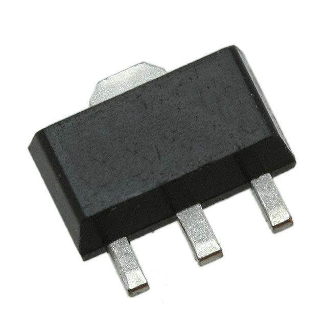
| 描述 | IC REG LDO 1.8V 1.5A SOT223-6低压差稳压器 Low-Noise Fast-Trans Resp 1.5A LDO Reg |
| DevelopmentKit | TPS7A4518EVM-385 |
| 产品分类 | |
| 品牌 | Texas Instruments |
| 产品手册 | |
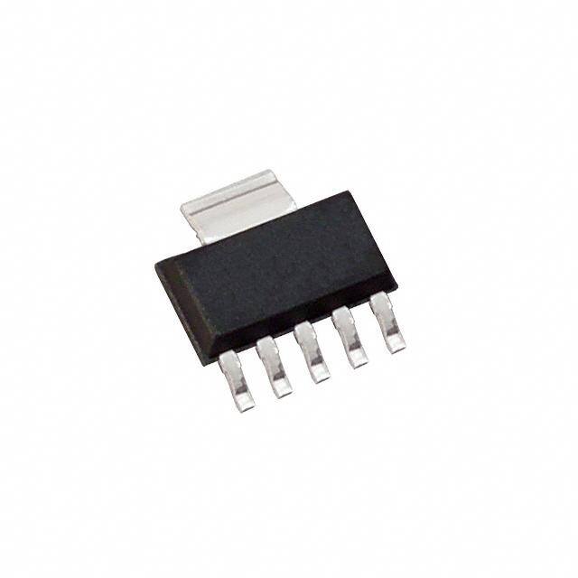
| 产品图片 |
|
| rohs | 符合RoHS无铅 / 符合限制有害物质指令(RoHS)规范要求 |
| 产品系列 | 电源管理 IC,低压差稳压器,Texas Instruments TPS7A4518DCQT- |
| 数据手册 | |
| 产品型号 | TPS7A4518DCQT |
| 产品种类 | 低压差稳压器 |
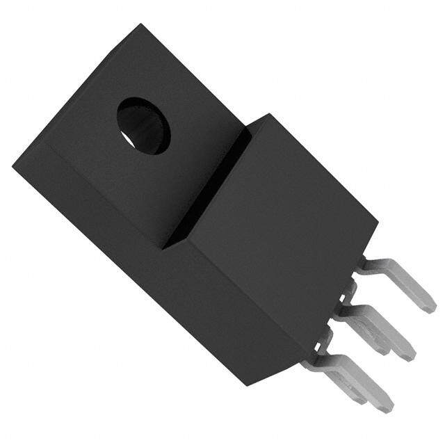
| 供应商器件封装 | SOT-223-6 |
| 包装 | 带卷 (TR) |
| 商标 | Texas Instruments |
| 回动电压—最大值 | 50 mV at 1 mA |
| 安装类型 | 表面贴装 |
| 封装 | Reel |
| 封装/外壳 | SOT-223-6 |
| 封装/箱体 | SOT-223-6 |
| 工作温度 | -40°C ~ 125°C |
| 工厂包装数量 | 250 |
| 最大工作温度 | + 125 C |
| 最大输入电压 | 20 V |
| 最小工作温度 | - 40 C |
| 最小输入电压 | 1.9 V |
| 标准包装 | 250 |
| 电压-跌落(典型值) | 0.3V @ 1.5A |
| 电压-输入 | 2.1 V ~ 20 V |
| 电压-输出 | 1.8V |
| 电压调节准确度 | 1 % |
| 电流-输出 | 1.5A |
| 电流-限制(最小值) | 1.6A |
| 稳压器拓扑 | 正,固定式 |
| 稳压器数 | 1 |
| 系列 | TPS7A4518 |
| 线路调整率 | 7 mV / V |
| 负载调节 | 10 mV |
| 输入偏压电流—最大 | 1 mA |
| 输出电压 | 1.8 V |
| 输出电流 | 1.5 A |
| 输出端数量 | 1 Output |
| 输出类型 | Fixed |


- 商务部:美国ITC正式对集成电路等产品启动337调查
- 曝三星4nm工艺存在良率问题 高通将骁龙8 Gen1或转产台积电
- 太阳诱电将投资9.5亿元在常州建新厂生产MLCC 预计2023年完工
- 英特尔发布欧洲新工厂建设计划 深化IDM 2.0 战略
- 台积电先进制程称霸业界 有大客户加持明年业绩稳了
- 达到5530亿美元!SIA预计今年全球半导体销售额将创下新高
- 英特尔拟将自动驾驶子公司Mobileye上市 估值或超500亿美元
- 三星加码芯片和SET,合并消费电子和移动部门,撤换高东真等 CEO
- 三星电子宣布重大人事变动 还合并消费电子和移动部门
- 海关总署:前11个月进口集成电路产品价值2.52万亿元 增长14.8%


PDF Datasheet 数据手册内容提取
Product Sample & Technical Tools & Support & Reference Folder Buy Documents Software Community Design TPS7A4501,TPS7A4515,TPS7A4518,TPS7A4525,TPS7A4533 SLVS720F–JUNE2008–REVISEDNOVEMBER2015 TPS7A45xx Low-Noise Fast-Transient-Response 1.5-A Low-Dropout Voltage Regulators 1 Features 3 Description • OptimizedforFastTransientResponse The TPS7A45xx devices are low-dropout (LDO) 1 regulators optimized for fast transient response. The • OutputCurrent:1.5A device can supply 1.5 A of output current with a • HighOutputVoltageAccuracy:1%at25°C dropout voltage of 300 mV. Operating quiescent • DropoutVoltage:300mV current is 1 mA, dropping to less than 1 μA in shutdown.Quiescentcurrentiswellcontrolled;itdoes • LowNoise:35 μV (10Hzto100kHz) RMS not rise in dropout as with many other regulators. In • HighRippleRejection:68dBat1kHz addition to fast transient response, the TPS7A45xx • 1-mAQuiescentCurrent regulators have very-low output noise, which makes themidealforsensitiveRFsupplyapplications. • NoProtectionDiodesNeeded • ControlledQuiescentCurrentinDropout Output voltage range is from 1.21 to 20 V. The TPS7A45xx regulators are stable with output • FixedOutputVoltages:1.5V,1.8V,2.5V,3.3V capacitance as low as 10 μF. Small ceramic • AdjustableOutputfrom1.21Vto20V capacitors can be used without the necessary (TPS7A4501Only) addition of ESR as is common with other regulators. • LessThan1-μAQuiescentCurrentinShutdown Internal protection circuitry includes reverse-battery protection, current limiting, thermal limiting, and • StableWith10-μFCeramicOutputCapacitor reverse-current protection. The devices are available • Reverse-BatteryProtection in fixed output voltages of 1.5 V, 1.8 V, 2.5 V, 3.3 V, • ReverseCurrentProtection and as an adjustable device with a 1.21-V reference voltage. 2 Applications DeviceInformation(1) • Industrial PARTNUMBER PACKAGE BODYSIZE(NOM) • WirelessInfrastructure SOT-223(6) 6.50mm×7.06mm • Radio-FrequencySystems TPS7A45xx TO-263(5) 10.16mm×15.24mm (1) For all available packages, see the orderable addendum at theendofthedatasheet. SimplifiedSchematic DropoutVoltagevsOutputCurrent 500 450 400 V 350 T =125°C m A – e 300 g a olt 250 V ut o 200 p o Dr 150 TA=25°C 100 50 0 0 0.2 0.4 0.6 0.8 1 1.2 1.4 1.6 OutputCurrent–A 1 An IMPORTANT NOTICE at the end of this data sheet addresses availability, warranty, changes, use in safety-critical applications, intellectualpropertymattersandotherimportantdisclaimers.PRODUCTIONDATA.
TPS7A4501,TPS7A4515,TPS7A4518,TPS7A4525,TPS7A4533 SLVS720F–JUNE2008–REVISEDNOVEMBER2015 www.ti.com Table of Contents 1 Features.................................................................. 1 8.4 DeviceFunctionalModes........................................16 2 Applications........................................................... 1 9 ApplicationandImplementation........................ 17 3 Description............................................................. 1 9.1 ApplicationInformation............................................17 4 RevisionHistory..................................................... 2 9.2 TypicalApplications................................................18 5 DeviceComparisonTable..................................... 3 10 PowerSupplyRecommendations..................... 22 6 PinConfigurationandFunctions......................... 3 11 Layout................................................................... 22 11.1 LayoutGuidelines.................................................22 7 Specifications......................................................... 4 11.2 LayoutExample....................................................23 7.1 AbsoluteMaximumRatings .....................................4 11.3 ThermalConsiderations........................................24 7.2 ESDRatings..............................................................4 12 DeviceandDocumentationSupport................. 26 7.3 RecommendedOperatingConditions.......................4 7.4 ThermalInformation..................................................5 12.1 RelatedLinks........................................................26 7.5 ElectricalCharacteristics...........................................5 12.2 CommunityResources..........................................26 7.6 TypicalCharacteristics..............................................8 12.3 Trademarks...........................................................26 12.4 ElectrostaticDischargeCaution............................26 8 DetailedDescription............................................ 13 12.5 Glossary................................................................26 8.1 Overview.................................................................13 13 Mechanical,Packaging,andOrderable 8.2 FunctionalBlockDiagram.......................................13 Information........................................................... 26 8.3 FeatureDescription.................................................13 4 Revision History NOTE:Pagenumbersforpreviousrevisionsmaydifferfrompagenumbersinthecurrentversion. ChangesfromRevisionE(August2014)toRevisionF Page • Correctedthebodysizeslistedforthepackages ................................................................................................................. 1 • MovedT toAbsoluteMaximumRatingstableandchangedHandlingRatingstoESDRatingstable............................... 4 stg • RelocatedThermalConsiderationsandCalculatingJunctionTemperaturetoLayout........................................................ 24 • AddedCommunityResources ............................................................................................................................................. 26 ChangesfromRevisionD(August2011)toRevisionE Page • AddedHandlingRatingtable,FeatureDescriptionsection,DeviceFunctionalModes,Applicationand Implementationsection,PowerSupplyRecommendationssection,Layoutsection,DeviceandDocumentation Supportsection,andMechanical,Packaging,andOrderableInformationsection ............................................................... 1 ChangesfromRevisionC(December2010)toRevisionD Page • ReplacedtheDissipationRatingstablewiththeThermalInformationtable.......................................................................... 5 2 SubmitDocumentationFeedback Copyright©2008–2015,TexasInstrumentsIncorporated ProductFolderLinks:TPS7A4501 TPS7A4515 TPS7A4518 TPS7A4525 TPS7A4533
TPS7A4501,TPS7A4515,TPS7A4518,TPS7A4525,TPS7A4533 www.ti.com SLVS720F–JUNE2008–REVISEDNOVEMBER2015 5 Device Comparison Table DEVICE OUTPUTVOLTAGE PIN5 TPS7A4501 Adjustable ADJ TPS7A4515 1.5V SENSE TPS7A4518 1.8V SENSE TPS7A4525 2.5V SENSE TPS7A4533 3.3V SENSE 6 Pin Configuration and Functions DCQPackage 6-PinSOT-223 KTTPackage TopView 6-PinTO-263 TopView 5 SENSE/ADJ 4 OUT 5 SENSE/ADJ D N 6 3 GND 4 OUT G 2 IN 3 GND 1 SHDN 2 IN 1 SHDN PinFunctions PIN DESCRIPTION NO. NAME Shutdown.SHDNisusedtoputtheTPS7A45xxregulatorsintoalow-powershutdownstate.Theoutputisoff whenSHDNispulledlow.SHDNcanbedrivenby5-Vlogic,3-Vlogicoropen-collectorlogicwithapullup 1 SHDN resistor.Thepullupresistorisrequiredtosupplythepullupcurrentoftheopen-collectorgate,normallyseveral microamperes,andSHDNcurrent,typically3μA.Ifunused,SHDNmustbeconnectedtoV .Thedeviceisin IN thelow-powershutdownstateifSHDNisnotconnected. Input.PowerissuppliedtothedevicethroughIN.Abypasscapacitorisrequiredonthispinifthedeviceismore thansixinchesawayfromthemaininputfiltercapacitor.Ingeneral,theoutputimpedanceofabatteryriseswith frequency,soitisadvisabletoincludeabypasscapacitorinbattery-poweredcircuits.Abypasscapacitor (ceramic)intherangeof1μFto10μFissufficient.TheTPS7A45xxregulatorsaredesignedtowithstand 2 IN reversevoltagesonINwithrespecttogroundandonOUT.Inthecaseofareverseinput,whichcanhappenifa batteryispluggedinbackwards,thedeviceactsasifthereisadiodeinserieswithitsinput.Thereisnoreverse currentflowintotheregulator,andnoreversevoltageappearsattheload.Thedeviceprotectsbothitselfand theload. Ground. 3 GND FortheKTTpackage,theexposedthermalpadisconnectedtoGNDandmustbesolderedtothePCBforrated thermalperformance. Output.Theoutputsuppliespowertotheload.Aminimumoutputcapacitor(ceramic)of10μFisrequiredto 4 OUT preventoscillations.Largeroutputcapacitorsarerequiredforapplicationswithlargetransientloadstolimitpeak voltagetransients. Adjust.Fortheadjustableversiononly(TPS7A4501),thisistheinputtotheerroramplifier.ADJisinternally 5 ADJ clampedto±7V.Ithasabiascurrentof3μAthatflowsintothepin.ADJvoltageis1.21Vreferencedtoground, andtheoutputvoltagerangeis1.21Vto20V. Sense.Forfixed-voltageversions(TPS7A4515,TPS7A4518,TPS7A4525,andTPS7A4533),SENSEisthe inputtotheerroramplifier.OptimumregulationisobtainedatthepointwhereSENSEisconnectedtotheOUT pinoftheregulator.Incriticalapplications,smallvoltagedropsarecausedbytheresistance(R )ofPCBtraces P betweentheregulatorandtheload.ThesemaybeeliminatedbyconnectingSENSEtotheoutputattheloadas 5 SENSE showninFigure32.NotethatthevoltagedropacrosstheexternalPCBtracesaddstothedropoutvoltageofthe regulator.SENSEbiascurrentis600μAattheratedoutputvoltage.SENSEcanbepulledbelowground(asina dualsupplysysteminwhichtheregulatorloadisreturnedtoanegativesupply)andstillallowthedevicetostart andoperate. 6 GND Ground.DCQpackageonly. Copyright©2008–2015,TexasInstrumentsIncorporated SubmitDocumentationFeedback 3 ProductFolderLinks:TPS7A4501 TPS7A4515 TPS7A4518 TPS7A4525 TPS7A4533
TPS7A4501,TPS7A4515,TPS7A4518,TPS7A4525,TPS7A4533 SLVS720F–JUNE2008–REVISEDNOVEMBER2015 www.ti.com 7 Specifications 7.1 Absolute Maximum Ratings overoperatingvirtual-junctiontemperaturerange(unlessotherwisenoted) (1) MIN MAX UNIT IN –20 20 OUT –20 20 Input-to-outputdifferential (2) –20 20 Inputvoltage,V V IN SENSE –20 20 ADJ –7 7 SHDN –20 20 Outputshort-circuitduration,t Indefinite short Maximumleadtemperature(10-ssolderingtime),T 300 °C lead Maximumjunctiontemperature,T 150 °C JMAX Storagetemperature,T –65 150 °C stg (1) StressesbeyondthoselistedunderAbsoluteMaximumRatingsmaycausepermanentdamagetothedevice.Thesearestressratings only,andfunctionaloperationofthedeviceattheseoranyotherconditionsbeyondthoseindicatedunderRecommendedOperating Conditionsisnotimplied.Exposuretoconditionsbeyondtherecommendedoperatingmaximumforextendedperiodsmayaffectdevice reliability. (2) Absolutemaximuminput-to-outputdifferentialvoltagecannotbeachievedwithallcombinationsofratedINpinandOUTpinvoltages. WiththeINpinat20V,theOUTpinmaynotbepulledbelow0V.ThetotalmeasuredvoltagefromINtoOUTcannotexceed±20V. 7.2 ESD Ratings VALUE UNIT Electrostatic Humanbodymodel(HBM),perANSI/ESDA/JEDECJS-001,allpins (1) ±2000 V V (ESD) discharge Chargeddevicemodel(CDM),perJEDECspecificationJESD22-C101,allpins (2) ±1000 (1) JEDECdocumentJEP155statesthat500-VHBMallowssafemanufacturingwithastandardESDcontrolprocess.Pinslistedas2000V mayactuallyhavehigherperformance. (2) JEDECdocumentJEP157statesthat250-VCDMallowssafemanufacturingwithastandardESDcontrolprocess.Pinslistedas1000V mayactuallyhavehigherperformance. 7.3 Recommended Operating Conditions overoperatingfree-airtemperaturerange(unlessotherwisenoted) MIN MAX UNIT V Inputvoltagerange(1) V +V 20 V IN OUT DO V SHDNhigh-levelinputvoltage 2 20 V IH V SHDNlow-levelinputvoltage 0.25 V IL T Recommendedoperatingjunctiontemperaturerange –40 125 °C J (1) TPS7A4501,TPS7A4515,andTPS7A4518mayrequireahigherminimuminputvoltageundersomeoutputvoltage/loadconditionsas indicatedunderElectricalCharacteristics. 4 SubmitDocumentationFeedback Copyright©2008–2015,TexasInstrumentsIncorporated ProductFolderLinks:TPS7A4501 TPS7A4515 TPS7A4518 TPS7A4525 TPS7A4533
TPS7A4501,TPS7A4515,TPS7A4518,TPS7A4525,TPS7A4533 www.ti.com SLVS720F–JUNE2008–REVISEDNOVEMBER2015 7.4 Thermal Information TPS7A45xx THERMALMETRIC (1) (2) KTT(TO-263) DCQ(SOT-223) UNIT 5PINS 6PINS R Junction-to-ambientthermalresistance 28.0 50.5 °C/W θJA R Junction-to-case(top)thermalresistance 43.0 31.1 °C/W θJC(top) R Junction-to-boardthermalresistance 17.4 5.1 °C/W θJB ψ Junction-to-topcharacterizationparameter 3.9 1.0 °C/W JT ψ Junction-to-boardcharacterizationparameter 9.4 5.0 °C/W JB R Junction-to-case(bottom)thermalresistance 0.3 — °C/W θJC(bot) (1) Formoreinformationabouttraditionalandnewthermalmetrics,seetheSemiconductorandICPackageThermalMetricsapplication report,SPRA953. (2) ForthermalestimatesofthisdevicebasedonPCBcopperarea,seetheTIPCBThermalCalculator. 7.5 Electrical Characteristics OverrecommendedoperatingtemperaturerangeT =–40to125°C(unlessotherwisenoted) (1) J PARAMETER TESTCONDITIONS T MIN TYP (2) MAX UNIT J I =0.5A 25°C 1.9 V Minimuminputvoltage (3) (4) LOAD V IN I =1.5A Fullrange 2.1 2.5 LOAD V =2.21V,I =1mA 25°C 1.485 1.5 1.515 IN LOAD TPS7A4515 V =2.5Vto20V, IN Fullrange 1.447 1.5 1.545 I =1mAto1.5A LOAD V =2.3V,I =1mA 25°C 1.782 1.8 1.818 IN LOAD TPS7A4518 V =2.8Vto20V, IN Fullrange 1.737 1.8 1.854 I =1mAto1.5A V Regulatedoutputvoltage (5) LOAD V OUT V =3V,I =1mA 25°C 2.475 2.5 2.525 IN LOAD TPS7A4525 V =3.5Vto20V, IN Fullrange 2.412 2.5 2.575 I =1mAto1.5A LOAD V =3.8V,I =1mA 25°C 3.266 3.3 3.333 IN LOAD TPS7A4533 V =4.3Vto20V, IN Fullrange 3.2 3.3 3.4 I =1mAto1.5A LOAD V =2.21V,I =1mA 25°C 1.197 1.21 1.222 IN LOAD VADJ ADJpinvoltage (3) (5) TPS7A4501 VIN=2.5Vto20V, Fullrange 1.174 1.21 1.246 V I =1mAto1.5A LOAD ΔV =2.21Vto20V, TPS7A4515 IN Fullrange 2 6 I =1mA LOAD ΔV =2.3Vto20V, TPS7A4518 IN Fullrange 2.5 7 I =1mA LOAD ΔV =3Vto20V, Lineregulation TPS7A4525 IN Fullrange 3 10 mV I =1mA LOAD ΔV =3.8Vto20V, TPS7A4533 IN Fullrange 3.5 10 I =1mA LOAD TPS7A4501 (3) ΔVIN=2.21Vto20V, Fullrange 1.5 3 I =1mA LOAD (1) TheTPS7A45xxregulatorsaretestedandspecifiedunderpulseloadconditionssuchthatT ≉T .TheyarefullytestedatT =25°C. J A A Performanceat–40and125°Cisspecifiedbydesign,characterization,andcorrelationwithstatisticalprocesscontrols. (2) Typicalvaluesrepresentthelikelyparametricnominalvaluesdeterminedatthetimeofcharacterization.Typicalvaluesdependonthe applicationandconfigurationandmayvaryovertime.Typicalvaluesarenotensuredonproductionmaterial. (3) TheTPS7A4501istestedandspecifiedfortheseconditionswiththeADJpinconnectedtotheOUTpin. (4) FortheTPS7A4501,TPS7A4515andTPS7A4518,dropoutvoltagesarelimitedbytheminimuminputvoltagespecificationundersome outputvoltage/loadconditions. (5) Operatingconditionsarelimitedbymaximumjunctiontemperature.Theregulatedoutputvoltagespecificationdoesnotapplyforall possiblecombinationsofinputvoltageandoutputcurrent.Whenoperatingatmaximuminputvoltage,theoutputcurrentrangemustbe limited.Whenoperatingatmaximumoutputcurrent,theinputvoltagerangemustbelimited. Copyright©2008–2015,TexasInstrumentsIncorporated SubmitDocumentationFeedback 5 ProductFolderLinks:TPS7A4501 TPS7A4515 TPS7A4518 TPS7A4525 TPS7A4533
TPS7A4501,TPS7A4515,TPS7A4518,TPS7A4525,TPS7A4533 SLVS720F–JUNE2008–REVISEDNOVEMBER2015 www.ti.com Electrical Characteristics (continued) OverrecommendedoperatingtemperaturerangeT =–40to125°C(unlessotherwisenoted)(1) J PARAMETER TESTCONDITIONS T MIN TYP (2) MAX UNIT J V =2.5V, 25°C 2 9 TPS7A4515 IN ΔILOAD=1mAto1.5A Fullrange 18 V =2.8V, 25°C 2 10 TPS7A4518 IN ΔILOAD=1mAto1.5A Fullrange 20 V =3.5V, 25°C 2.5 15 TPS7A4525 IN ΔILOAD=1mAto1.5A Fullrange 30 Loadregulation 25°C 3 20 mV V =4.3V, -40to+85 TPS7A4533 IN 30 ΔI =1mAto1.5A °C LOAD Fullrange 70 25°C 2 8 TPS7A4501 (3) VIN=2.5V, -40to+85 8 ΔI =1mAto1.5A °C LOAD Fullrange 18 25°C 0.02 0.05 I =1mA LOAD Fullrange 0.06 25°C 0.085 0.10 I =100mA LOAD Dropoutvoltage (4) (6) (7) Fullrange 0.13 V V DO VIN=VOUT(NOMINAL) 25°C 0.17 0.180 I =500mA LOAD Fullrange 0.250 25°C 0.300 0.350 I =1.5A LOAD Fullrange 0.450 I =0mA Fullrange 1 1.5 LOAD I =1mA Fullrange 1.1 1.6 LOAD GNDpincurrent (7) (8) I I =100mA Fullrange 3.3 3.5 mA GND V =V +1 LOAD IN OUT(NOMINAL) I =500mA Fullrange 15 17 LOAD I =1.5A Fullrange 80 90 LOAD C =10μF,I =1.5A, e Outputvoltagenoise OUT LOAD 25°C 35 μV N B =10Hzto100kHz RMS W I ADJpinbiascurrent (3) (9) 25°C 3 7 μA ADJ V =OFFtoON Fullrange 0.9 2 OUT Shutdownthreshold V V =ONtoOFF Fullrange 0.25 0.75 OUT V =0V 25°C 0.01 1 SHDN I SHDNpincurrent μA SHDN V =20V 25°C 3 20 SHDN Quiescentcurrentinshutdown V =6V,V =0V 25°C 0.01 1 μA IN SHDN V –V =1.5V(avg),V =0.5V , Ripplerejection IN OUT RIPPLE P-P 25°C 68 dB f =120Hz,I =0.75A RIPPLE LOAD V =7V,V =0V 25°C 2 IN OUT I Currentlimit A LIMIT V =V +1 Fullrange 1.6 IN OUT(NOMINAL) I Inputreverseleakagecurrent V =–20V,V =0V Fullrange 300 μA IL IN OUT (6) Dropoutvoltageistheminimuminputtooutputvoltagedifferentialneededtomaintainregulationataspecifiedoutputcurrent.In dropout,theoutputvoltageisequalto:V –V . IN DROPOUT (7) Tosatisfyrequirementsforminimuminputvoltage,theTPS7A4501istestedandspecifiedfortheseconditionswithanexternalresistor divider(two4.12-kΩresistors)foranoutputvoltageof2.4V.Theexternalresistordivideraddsa300-µADCloadontheoutput. (8) GNDpincurrentistestedwithV =(V +1V)andacurrentsourceload.TheGNDpincurrentdecreasesathigherinput IN OUT(NOMINAL) voltages. (9) ADJpinbiascurrentflowsintotheADJpin. 6 SubmitDocumentationFeedback Copyright©2008–2015,TexasInstrumentsIncorporated ProductFolderLinks:TPS7A4501 TPS7A4515 TPS7A4518 TPS7A4525 TPS7A4533
TPS7A4501,TPS7A4515,TPS7A4518,TPS7A4525,TPS7A4533 www.ti.com SLVS720F–JUNE2008–REVISEDNOVEMBER2015 Electrical Characteristics (continued) OverrecommendedoperatingtemperaturerangeT =–40to125°C(unlessotherwisenoted)(1) J PARAMETER TESTCONDITIONS T MIN TYP (2) MAX UNIT J TPS7A4515 V =1.5V,V <1.5V 25°C 600 1000 OUT IN TPS7A4518 V =1.8V,V <1.8V 25°C 600 1000 OUT IN I Reverseoutputcurrent (10) TPS7A4525 V =2.5V,V <2.5V 25°C 600 1000 μA RO OUT IN TPS7A4533 V =3.3V,V <3.3V 25°C 600 1000 OUT IN TPS7A4501 V =1.21V,V <1.21V 25°C 300 500 OUT IN (10) ReverseoutputcurrentistestedwiththeINpingroundedandtheOUTpinforcedtotheratedoutputvoltage.Thiscurrentflowsintothe OUTpinandouttheGNDpin. Copyright©2008–2015,TexasInstrumentsIncorporated SubmitDocumentationFeedback 7 ProductFolderLinks:TPS7A4501 TPS7A4515 TPS7A4518 TPS7A4525 TPS7A4533
TPS7A4501,TPS7A4515,TPS7A4518,TPS7A4525,TPS7A4533 SLVS720F–JUNE2008–REVISEDNOVEMBER2015 www.ti.com 7.6 Typical Characteristics TypicalcharacteristicsapplytoallTPS7A45xxdevicesunlessotherwisenoted. 500 480 450 IOUT=1.5A 400 360 mV350 TA=125°C mV DropoutVoltage–122350500000 TA=25°C DropoutVoltage–240 IOUT=0.5A 120 IOUT=100mA 100 50 IOUT=1mA 0 0 0 0.2 0.4 0.6 0.8 1 1.2 1.4 1.6 -50 -25 0 25 50 75 100 125 OutputCurrent–A TA–Free-AirTemperature–°C Figure1.DropoutVoltagevsOutputCurrent Figure2.DropoutVoltagevsTemperature V =6V I =0A V =VIN I =1mA TPS7A4518 IN OUT SHDN OUT Figure3.QuiescentCurrentvsTemperature Figure4.TPS7A4518OutputVoltagevsTemperature I =1mA TPS7A4525 I =1mA TPS7A4533 OUT OUT Figure5.TPS7A4525OutputVoltagevsTemperature Figure6.TPS7A4533OutputVoltagevsTemperature 8 SubmitDocumentationFeedback Copyright©2008–2015,TexasInstrumentsIncorporated ProductFolderLinks:TPS7A4501 TPS7A4515 TPS7A4518 TPS7A4525 TPS7A4533
TPS7A4501,TPS7A4515,TPS7A4518,TPS7A4525,TPS7A4533 www.ti.com SLVS720F–JUNE2008–REVISEDNOVEMBER2015 Typical Characteristics (continued) TypicalcharacteristicsapplytoallTPS7A45xxdevicesunlessotherwisenoted. 1.23 1.2 1.225 1 1.22 A) Output Voltage (V) 111..22.201155 Quiescent Current (m 000...468 1.2 0.2 1.195 0 1.19 0 2 4 6 8 10 12 14 16 18 20 -50 -25 0 25 50 75 100 125 Input Voltage (V) D021 Free-Air Temperature (qC) T =25°C R =4.3kΩ D020 J OUT IOUT=1mA VIN=6V VSHDN=VIN Figure7.TPS7A4501OutputVoltagevsTemperature Figure8.QuiescentCurrentvsInputVoltage 10 9 IIOOUUTT == 1100 0m mAA 8 IOUT = 300 mA A) 7 m nt ( 6 e urr 5 C d 4 n u Gro 3 2 1 0 0 1 2 3 4 5 6 7 8 9 10 Input Voltage (V) D022 TJ=25°C VOUT=1.21V TJ=25°C VOUT=1.21V VSHDN=VIN VSHDN=VIN Figure9.TPS7A4501GroundCurrentvsInputVoltage Figure10.TPS7A4501GroundCurrentvsInputVoltage T =25°C V =V T =25°C V =V J SHDN IN J SHDN IN Figure12.TPS7A4533GroundCurrentvsInputVoltage Figure11.TPS7A4533GroundCurrentvsInputVoltage Copyright©2008–2015,TexasInstrumentsIncorporated SubmitDocumentationFeedback 9 ProductFolderLinks:TPS7A4501 TPS7A4515 TPS7A4518 TPS7A4525 TPS7A4533
TPS7A4501,TPS7A4515,TPS7A4518,TPS7A4525,TPS7A4533 SLVS720F–JUNE2008–REVISEDNOVEMBER2015 www.ti.com Typical Characteristics (continued) TypicalcharacteristicsapplytoallTPS7A45xxdevicesunlessotherwisenoted. VIN=VOUT(nom)+1 VSHDN=0V Figure13.GroundCurrentvsOutputCurrent Figure14.QuiescentCurrentinShutdownvsInputVoltage 2.5 2.25 2 A µ1.75 – ent 1.5 urr C1.25 ut p In 1 N D H0.75 S 0.5 0.25 0 0 2 4 6 8 10 12 14 16 18 20 SHDNInputVoltage–V V =0V SHON Figure15. SHDNPinCurrent(ISHDN)vsTemperature Figure16. SHDNPinCurrent(ISHDN)vsSHDNInputVoltage I =1mA I =1mA OUT OUT Figure18. SHDNThreshold(ONtoOFF)vsTemperature Figure17. SHDNThreshold(OFFtoON)vsTemperature 10 SubmitDocumentationFeedback Copyright©2008–2015,TexasInstrumentsIncorporated ProductFolderLinks:TPS7A4501 TPS7A4515 TPS7A4518 TPS7A4525 TPS7A4533
TPS7A4501,TPS7A4515,TPS7A4518,TPS7A4525,TPS7A4533 www.ti.com SLVS720F–JUNE2008–REVISEDNOVEMBER2015 Typical Characteristics (continued) TypicalcharacteristicsapplytoallTPS7A45xxdevicesunlessotherwisenoted. 5 4.5 4 A3.5 µ – Current2.53 Bias 2 DJ A1.5 1 0.5 0 -50 -25 0 25 50 75 100 125 TA–Free-AirTemperature–°C ΔV =100mV OUT Figure19.ADJBiasCurrentvsTemperature Figure20.CurrentLimitvsInput-to-OutputDifferential Voltage T =25°C V =0V J IN VIN=7V VOUT=0V CurrentflowsintoOUTpin Figure21.CurrentLimitvsTemperature Figure22.ReverseOutputCurrentvsOutputVoltage V =0.05V C =0 T =25°C RIPPLE PP IN A V =0V V =2.7V C =10µF(ceramic) IN IN OUT Figure23.ReverseOutputCurrentvsTemperature Figure24.RippleRejectionvsFrequency Copyright©2008–2015,TexasInstrumentsIncorporated SubmitDocumentationFeedback 11 ProductFolderLinks:TPS7A4501 TPS7A4515 TPS7A4518 TPS7A4525 TPS7A4533
TPS7A4501,TPS7A4515,TPS7A4518,TPS7A4525,TPS7A4533 SLVS720F–JUNE2008–REVISEDNOVEMBER2015 www.ti.com Typical Characteristics (continued) TypicalcharacteristicsapplytoallTPS7A45xxdevicesunlessotherwisenoted. I =1.5A OUT C =10µF I =1.5A OUT OUT (ceramic) Figure25.LoadRegulationvsTemperature Figure26.OutputNoiseVoltagevsFrequency V =4.3V C =10µF V =4.3V C =10µF IN IN IN IN C =10µF(ceramic) C =10µF(ceramic) OUT OUT Figure27.LoadTransientResponse Figure28.LoadTransientResponse I =1.5A C =10µF OUT IN C =10µF(ceramic) OUT Figure29.LineTransientResponse 12 SubmitDocumentationFeedback Copyright©2008–2015,TexasInstrumentsIncorporated ProductFolderLinks:TPS7A4501 TPS7A4515 TPS7A4518 TPS7A4525 TPS7A4533
TPS7A4501,TPS7A4515,TPS7A4518,TPS7A4525,TPS7A4533 www.ti.com SLVS720F–JUNE2008–REVISEDNOVEMBER2015 8 Detailed Description 8.1 Overview The TPS7A45xx series are 1.5-A low-dropout regulators optimized for fast transient response. The devices are capable of supplying 1.5 A at a dropout voltage of 300 mV. The low operating quiescent current (1 mA) drops to less than 1 μA in shutdown. In addition to the low quiescent current, the TPS7A45xx regulators incorporate several protection features that make them ideal for use in battery-powered systems. The devices are protected against both reverse input and reverse output voltages. In battery-backup applications where the output can be held up by a backup battery when the input is pulled to ground, the TPS7A45xx acts as if it has a diode in series with its output and prevents reverse current flow. Additionally, in dual-supply applications where the regulator loadisreturnedtoanegativesupply,theoutputcanbepulledbelowgroundbyasmuchas(20V – VIN)andstill allowthedevicetostartandoperate. 8.2 Functional Block Diagram Reverse Pass Current IN Current OUT Element Limit Protection SHDN Error Amplifier + Thermal SENSE/ADJ Overload + Voltage Reference Reverse Voltage Protection GND 8.3 Feature Description 8.3.1 AdjustableOperation The TPS7A4501 has an adjustable output voltage range of 1.21 V to 20 V. The output voltage is set by the ratio of two external resistors as shown in Figure 30. The device maintains the voltage at the ADJ pin at 1.21 V referenced to ground. The current in R1 is then equal to (1.21 V/R1), and the current in R2 is the current in R1 plus the ADJ pin bias current. The ADJ pin bias current, 3 μA at 25°C, flows through R2 into the ADJ pin. The output voltage can be calculated using the formula shown in Equation 1. The value of R1 should be less than 4.17 kΩ to minimize errors in the output voltage caused by the ADJ pin bias current. Note that in shutdown the outputisturnedoff,andthedividercurrentiszero. Copyright©2008–2015,TexasInstrumentsIncorporated SubmitDocumentationFeedback 13 ProductFolderLinks:TPS7A4501 TPS7A4515 TPS7A4518 TPS7A4525 TPS7A4533
TPS7A4501,TPS7A4515,TPS7A4518,TPS7A4525,TPS7A4533 SLVS720F–JUNE2008–REVISEDNOVEMBER2015 www.ti.com Figure30. AdjustableOperation Theoutputvoltagecanbesetusingthefollowingequations: R2 V =1.21V(1+ )+I ´R2 OUT ADJ R1 (1) V =1.21V (2) ADJ I =3µAat25°C (3) ADJ OutputRange=1.21to20V (4) 8.3.2 FixedOperation The TPS7A45xx can be used in a fixed voltage configuration. The SENSE/ADJ pin should be connected to OUT for proper operation. An example of this is shown in Figure 31. The TPS7A4501 can also be used in this configurationforafixedoutputvoltageof1.21V. IN OUT 2.5V at 1.5 A 10 µF 10 µF TPS7A4525 VIN> 3V (ceramic) (ceramic) SHDN SENSE GND Figure31. 3.3to2.5VRegulator During fixed voltage operation, the SENSE/ADJ pin can be used for a Kelvin connection if routed separately to the load. This allows the regulator to compensate for voltage drop across parasitic resistances (RP) between the outputandtheload.Thisbecomesmorecrucialwithhigherloadcurrents. R P IN OUT TPS7A4501 VIN SHDN SENSE Load GND R P Figure32. KelvinSenseConnection 14 SubmitDocumentationFeedback Copyright©2008–2015,TexasInstrumentsIncorporated ProductFolderLinks:TPS7A4501 TPS7A4515 TPS7A4518 TPS7A4525 TPS7A4533
TPS7A4501,TPS7A4515,TPS7A4518,TPS7A4525,TPS7A4533 www.ti.com SLVS720F–JUNE2008–REVISEDNOVEMBER2015 8.3.3 OverloadRecovery Like many IC power regulators, the TPS7A45xx has safe operating area protection. The safe area protection decreases the current limit as input-to-output voltage increases and keeps the power transistor inside a safe operating region for all values of input-to-output voltage. The protection is designed to provide some output currentatallvaluesofinput-to-outputvoltageuptothedevicebreakdown. When power is first turned on, as the input voltage rises, the output follows the input, allowing the regulator to start up into very heavy loads. During start up, as the input voltage is rising, the input-to-output voltage differential is small, allowing the regulator to supply large output currents. With a high input voltage, a problem can occur wherein removal of an output short does not allow the output voltage to recover. Other regulators also exhibitthisphenomenon,soitisnotuniquetotheTPS7A45xx. The problem occurs with a heavy output load when the input voltage is high and the output voltage is low. Common situations occur immediately after the removal of a short circuit or when the shutdown pin is pulled high after the input voltage has already been turned on. The load line for such a load may intersect the output current curve at two points. If this happens, there are two stable output operating points for the regulator. With this double intersection, the input power supply may need to be cycled down to zero and brought up again to make theoutputrecover. 8.3.4 OutputVoltageNoise The TPS7A45xx regulators have been designed to provide low output voltage noise over the 10-Hz to 100-kHz bandwidth while operating at full load. Output voltage noise is typically 35 nV/√Hz over this frequency bandwidth for the TPS7A4501 (adjustable version). For higher output voltages (generated by using a resistor divider), the output voltage noise is gained up accordingly. This results in RMS noise over the 10-Hz to 100-kHz bandwidth of 14μV fortheTPS7A4501,increasingto38 μV fortheTPS7A4533. RMS RMS Higher values of output voltage noise may be measured when care is not exercised with regard to circuit layout and testing. Crosstalk from nearby traces can induce unwanted noise onto the output of the TPS7A45xx. Power- supply ripple rejection must also be considered; the TPS7A45xx regulators do not have unlimited power-supply rejectionandpassasmallportionoftheinputnoisethroughtotheoutput. 8.3.5 ProtectionFeatures The TPS7A45xx regulators incorporate several protection features which make them ideal for use in battery- powered circuits. In addition to the normal protection features associated with monolithic regulators, such as current limiting and thermal limiting, the devices are protected against reverse input voltages, reverse output voltagesandreversevoltagesfromoutputtoinput. Current limit protection and thermal overload protection are intended to protect the device against current overloadconditionsattheoutputofthedevice.Fornormaloperation,thejunctiontemperatureshouldnotexceed 125°C. The input of the device withstands reverse voltages of 20 V. Current flow into the device is limited to less than 1 mA (typically less than 100 μA), and no negative voltage appears at the output. The device protects both itself andtheload.Thisprovidesprotectionagainstbatteriesthatcanbepluggedinbackward. The output of the TPS7A45xx can be pulled below ground without damaging the device. If the input is left open circuit or grounded, the output can be pulled below ground by 20 V. For fixed voltage versions, the output acts like a large resistor, typically 5 kΩ or higher, limiting current flow to typically less than 600 μA. For adjustable versions, the output acts like an open circuit; no current flows out of the pin. If the input is powered by a voltage source, the output sources the short-circuit current of the device and protects itself by thermal limiting. In this case,groundingtheSHDNpinturnsoffthedeviceandstopstheoutputfromsourcingtheshort-circuitcurrent. The ADJ pin of the adjustable device can be pulled above or below ground by as much as 7 V without damaging the device. If the input is left open circuit or grounded, the ADJ pin acts like an open circuit when pulled below groundandlikealargeresistor(typically5kΩ)inserieswithadiodewhenpulledaboveground. In situations where the ADJ pin is connected to a resistor divider that would pull the ADJ pin above its 7-V clamp voltage if the output is pulled high, the ADJ pin input current must be limited to less than 5 mA. For example, a resistordividerisusedtoprovidearegulated1.5-Voutputfromthe1.21-Vreferencewhentheoutputisforcedto 20 V. The top resistor of the resistor divider must be chosen to limit the current into the ADJ pin to less than 5 mA when the ADJ pin is at 7 V. The 13-V difference between OUT and ADJ divided by the 5-mA maximum currentintotheADJpinyieldsaminimumtopresistorvalueof2.6kΩ. Copyright©2008–2015,TexasInstrumentsIncorporated SubmitDocumentationFeedback 15 ProductFolderLinks:TPS7A4501 TPS7A4515 TPS7A4518 TPS7A4525 TPS7A4533
TPS7A4501,TPS7A4515,TPS7A4518,TPS7A4525,TPS7A4533 SLVS720F–JUNE2008–REVISEDNOVEMBER2015 www.ti.com In circuits where a backup battery is required, several different input/output conditions can occur. The output voltage may be held up while the input is either pulled to ground, pulled to some intermediate voltage, or is left opencircuit. When the IN pin of the TPS7A45xx is forced below the OUT pin or the OUT pin is pulled above the IN pin, input current typically drops to less than 2 μA. This can happen if the input of the device is connected to a discharged (low voltage) battery and the output is held up by either a backup battery or a second regulator circuit. The state oftheSHDNpinhasnoeffectonthereverseoutputcurrentwhentheoutputispulledabovetheinput. 8.4 Device Functional Modes Table1showsthefunctionalmodesfortheTPS7A45xx. Table1.DeviceModes SHDN DEVICESTATE H Regulatedvoltage L Shutdown 16 SubmitDocumentationFeedback Copyright©2008–2015,TexasInstrumentsIncorporated ProductFolderLinks:TPS7A4501 TPS7A4515 TPS7A4518 TPS7A4525 TPS7A4533
TPS7A4501,TPS7A4515,TPS7A4518,TPS7A4525,TPS7A4533 www.ti.com SLVS720F–JUNE2008–REVISEDNOVEMBER2015 9 Application and Implementation NOTE Information in the following applications sections is not part of the TI component specification, and TI does not warrant its accuracy or completeness. TI’s customers are responsible for determining suitability of components for their purposes. Customers should validateandtesttheirdesignimplementationtoconfirmsystemfunctionality. 9.1 Application Information Thissectionhighlightssomedesignconsiderationsforimplementingthisdeviceinvariousapplications. 9.1.1 OutputCapacitanceandTransientResponse The TPS7A45xx regulators are designed to be stable with a wide range of output capacitors. The ESR of the output capacitor affects stability, most notably with small capacitors. A minimum output capacitor of 10 μF with anESRof3Ω orlessisrecommendedtopreventoscillations.Largervaluesofoutputcapacitancecandecrease the peak deviations and provide improved transient response for larger load current changes. Bypass capacitors, used to decouple individual components powered by the TPS7A45xx, increase the effective output capacitor value. Extra consideration must be given to the use of ceramic capacitors. Ceramic capacitors are manufactured with a variety of dielectrics, each with different behavior over temperature and applied voltage. The most common dielectrics used are Z5U, Y5V, X5R and X7R. The Z5U and Y5V dielectrics are good for providing high capacitances in a small package, but exhibit strong voltage and temperature coefficients. When used with a 5-V regulator, a 10-μF Y5V capacitor can exhibit an effective value as low as 1 μF to 2 μF over the operating temperature range. The X5R and X7R dielectrics result in more stable characteristics and are more suitable for use as the output capacitor. The X7R type has better stability across temperature, while the X5R is less expensiveandisavailableinhighervalues. Voltage and temperature coefficients are not the only sources of problems. Some ceramic capacitors have a piezoelectric response. A piezoelectric device generates voltage across its terminals due to mechanical stress, similar to the way a piezoelectric accelerometer or microphone works. For a ceramic capacitor, the stress can be inducedbyvibrationsinthesystemorthermaltransients. Copyright©2008–2015,TexasInstrumentsIncorporated SubmitDocumentationFeedback 17 ProductFolderLinks:TPS7A4501 TPS7A4515 TPS7A4518 TPS7A4525 TPS7A4533
TPS7A4501,TPS7A4515,TPS7A4518,TPS7A4525,TPS7A4533 SLVS720F–JUNE2008–REVISEDNOVEMBER2015 www.ti.com 9.2 Typical Applications 9.2.1 AdjustableOutputOperation IN OUT 2.5 V at 1 A R2 V = 5 V + C1 4.22 k(cid:13) C2 IN 10 PF TPS7A4501 10 PF SHDN ADJ GND R1 4 k(cid:13) NOTE: Allcapacitorsareceramic. Figure33. AdjustableOutputVoltageOperation 9.2.1.1 DesignRequirements Table2showsthedesignrequirements. Table2.DesignParameters DESIGNPARAMETER EXAMPLEVALUE Inputvoltage(V ) 5.0V IN Outputvoltage(V ) 2.5V OUT Outputcurrent(I ) 0to1A OUT Loadregulation 1% 9.2.1.2 DetailedDesignProcedure The TPS7A4501 has an adjustable output voltage range of 1.21 to 20 V. The output voltage is set by the ratio of two external resistors R1 and R2 as shown in Figure 33. The device maintains the voltage at the ADJ pin at 1.21 V referenced to ground. The current in R1 is then equal to (1.21 V/R1), and the current in R2 is the current in R1 plus the ADJ pin bias current. The ADJ pin bias current, 3 µA at 25°C, flows through R2 into the ADJ pin. The outputvoltagecanbecalculatedusingEquation5. R2 V =1.21V(1+ )+I ´R2 OUT ADJ R1 (5) The value of R1 should be less than 4.17 kΩ to minimize errors in the output voltage caused by the ADJ pin bias current. Note that in shutdown the output is turned off, and the divider current is zero. For an output voltage of 2.50V,R1willbesetto4.0kΩ.R2isthenfoundtobe4.22kΩ usingtheequationabove. 4.22kW V =1.21V(1+ )+3µA´4.22kW OUT 4.0kW (6) V =2.50V (7) OUT The adjustable device is tested and specified with the ADJ pin tied to the OUT pin for an output voltage of 1.21 V.Specificationsforoutputvoltagesgreaterthan1.21Vareproportionaltotheratioofthedesiredoutputvoltage to1.21V:V /1.21V.Forexample,loadregulationforanoutputcurrentchangeof1mAto1.5Ais –2mV(typ) OUT atV =1.21V.AtV =2.50V,thetypicalloadregulationis: OUT OUT (2.50V/1.21V)(–2mV)=–4.13mV (8) Figure 34 shows the actual change in output is about 3 mV for a 1-A load step. The maximum load regulation at 25°Cis–8mV.AtV =2.50V,themaximumloadregulationis: OUT (2.50V/1.21V)(–8mV)=–16.53mV (9) Because 16.53 mV is only 0.7% of the 2.5 V output voltage, the load regulation will meet the design requirements. 18 SubmitDocumentationFeedback Copyright©2008–2015,TexasInstrumentsIncorporated ProductFolderLinks:TPS7A4501 TPS7A4515 TPS7A4518 TPS7A4525 TPS7A4533
TPS7A4501,TPS7A4515,TPS7A4518,TPS7A4525,TPS7A4533 www.ti.com SLVS720F–JUNE2008–REVISEDNOVEMBER2015 9.2.1.3 ApplicationCurve Figure34. 1-ALoadTransientResponse Copyright©2008–2015,TexasInstrumentsIncorporated SubmitDocumentationFeedback 19 ProductFolderLinks:TPS7A4501 TPS7A4515 TPS7A4518 TPS7A4525 TPS7A4533
TPS7A4501,TPS7A4515,TPS7A4518,TPS7A4525,TPS7A4533 SLVS720F–JUNE2008–REVISEDNOVEMBER2015 www.ti.com 9.2.2 ParallelingRegulatorsforHigherOutputCurrent NOTE: Allcapacitorsareceramic. Figure35. ParallelingRegulatorsforHigherOutputCurrent 9.2.2.1 DesignRequirements Table3showsthedesignrequirements. Table3.DesignRequirements DESIGNPARAMETER EXAMPLEVALUE Inputvoltage(V ) 6.0V IN Outputvoltage(V ) 3.3V OUT Outputcurrent(I ) 3.0A OUT 9.2.2.2 DetailedDesignProcedure In an application requiring higher output current, an adjustable output regular can be placed in parallel with a fixed output regulator to increase the current capacity. Two sense resistors and a comparator can be used to controlthefeedbackloopoftheadjustableregulatorinordertobalancethecurrentbetweenthetworegulators. In Figure 35 resistors R1 and R2 are used to sense the current flowing into each regulator and should have a very low resistance to avoid unnecessary power loss. R1 and R2 should have the same value and a tolerance of 1% or better so the current is shared equally between the regulators. For this example, a value of 0.01 Ω will be used. 20 SubmitDocumentationFeedback Copyright©2008–2015,TexasInstrumentsIncorporated ProductFolderLinks:TPS7A4501 TPS7A4515 TPS7A4518 TPS7A4525 TPS7A4533
TPS7A4501,TPS7A4515,TPS7A4518,TPS7A4525,TPS7A4533 www.ti.com SLVS720F–JUNE2008–REVISEDNOVEMBER2015 The TLV3691 rail-to-rail nanopower comparator output will alternate between VIN and GND depending on the currents flowing into each of the two regulators. To design this control circuit, begin by looking at the case where the two output currents are approximately equal and the comparator output is low. In this case, the output of the TPS7A4501 should be set the same as the fixed voltage regulator. The TPS7A4533 has a 3.3 V fixed output, so this will be the set point for the adjustable regulator. Begin by selecting a R7 value less than 4.17 kΩ. In this example, 3.3 kΩ will be used. R5 will need to have a high resistance to satisfy Equation 14, for this example 100 kΩ was chosen. Then find the parallel resistance of R5 and R7 since they are both connected from the ADJ pin toGNDusingEquation10. R5´R7 (R5||R7)= =3.19kΩ R5+R7 (10) OncetheR5andR7parallelresistanceincalculated,thevalueforR6canbefoundusingEquation11. V R6= OUT (R5||R7)-(R5||R7) 1.22V (11) 3.3V R6= (3.19kW)-(3.19kW) 1.22V (12) R6=5.45kΩ (13) InthecasewheretheTPS7A4533issourcingmorecurrentthanTPS7A4501,thecomparatoroutputwillgohigh. This will lower the voltage at the ADJ pin causing the TPS7A4501 to try and raise the output voltage by sourcing more current. The TPS7A4533 will then react by sourcing less current to try and keep the output from rising. When the current through the TPS7A4533 becomes less than the TPS7A4501, the comparator output will return toGND.Inorderforthistohappen,Equation14mustbesatisfied: æ R7 ö æ R6 ö VINçèR5+R7÷ø+(VIN-VOUT)çèR5+R6÷ø< Vref (14) æ 3.3kW ö æ 5.45kW ö 6Vç ÷+(2.7V)ç ÷ <1.21V è100kW+3.3kWø è100kW+5.45kWø (15) 0.19V+0.14V<1.21V (16) 0.33V<1.21V (17) 9.2.2.3 ApplicationCurve Figure36. ParallelRegulatorsSharingLoadCurrent Copyright©2008–2015,TexasInstrumentsIncorporated SubmitDocumentationFeedback 21 ProductFolderLinks:TPS7A4501 TPS7A4515 TPS7A4518 TPS7A4525 TPS7A4533
TPS7A4501,TPS7A4515,TPS7A4518,TPS7A4525,TPS7A4533 SLVS720F–JUNE2008–REVISEDNOVEMBER2015 www.ti.com 10 Power Supply Recommendations The device is designed to operate with an input voltage supply up to 20 V. The minimum input voltage should provideadequateheadroomgreaterthanthedropoutvoltageinorderforthedevicetohavearegulatedoutput.If the input supply is noisy, additional input capacitors with low ESR can help improve the output noise performance. 11 Layout 11.1 Layout Guidelines 1. Forbestperformance,alltracesshouldbeasshortaspossible. 2. UsewidetracesforIN,OUT,andGNDtominimizetheparasiticelectricaleffects. 3. A minimum output capacitor of 10 μF with an ESR of 3 Ω or less is recommended to prevent oscillations. X5RandX7Rdielectricsarepreferred. 4. PlacetheOutputCapacitorascloseaspossibletotheOUTpinofthedevice. 5. ThetaboftheDCQpackageshouldbeconnectedtoground. 6. The exposed thermal pad of the KTT package should be connected to a wide ground plane for effective heat dissipation. 22 SubmitDocumentationFeedback Copyright©2008–2015,TexasInstrumentsIncorporated ProductFolderLinks:TPS7A4501 TPS7A4515 TPS7A4518 TPS7A4525 TPS7A4533
TPS7A4501,TPS7A4515,TPS7A4518,TPS7A4525,TPS7A4533 www.ti.com SLVS720F–JUNE2008–REVISEDNOVEMBER2015 11.2 Layout Example Figure37. TO-263LayoutExample(KTT) Copyright©2008–2015,TexasInstrumentsIncorporated SubmitDocumentationFeedback 23 ProductFolderLinks:TPS7A4501 TPS7A4515 TPS7A4518 TPS7A4525 TPS7A4533
TPS7A4501,TPS7A4515,TPS7A4518,TPS7A4525,TPS7A4533 SLVS720F–JUNE2008–REVISEDNOVEMBER2015 www.ti.com Layout Example (continued) Figure38. SOT-223LayoutExample(DCQ) 11.3 Thermal Considerations The power handling capability of the device is limited by the recommended maximum operating junction temperature(125°C).Thepowerdissipatedbythedeviceismadeupoftwocomponents: 1. Outputcurrentmultipliedbytheinput/outputvoltagedifferential:I (V –V ) OUT IN OUT 2. GNDpincurrentmultipliedbytheinputvoltage:I V GND IN The GND pin current can be found using the GND pin current graphs in Typical Characteristics. Power dissipationisequaltothesumofthetwocomponentslistedabove. The TPS7A45xx series regulators have internal thermal limiting designed to protect the device during overload conditions. For continuous normal conditions, the recommended maximum operating junction temperature is 125°C. It is important to give careful consideration to all sources of thermal resistance from junction to ambient. Additionalheatsourcesmountednearbymustalsobeconsidered. Forsurface-mountdevices,heatsinkingisaccomplishedbyusingtheheat-spreadingcapabilitiesofthePCBand its copper traces. Copper board stiffeners and plated through-holes can also be used to spread the heat generatedbypowerdevices. 24 SubmitDocumentationFeedback Copyright©2008–2015,TexasInstrumentsIncorporated ProductFolderLinks:TPS7A4501 TPS7A4515 TPS7A4518 TPS7A4525 TPS7A4533
TPS7A4501,TPS7A4515,TPS7A4518,TPS7A4525,TPS7A4533 www.ti.com SLVS720F–JUNE2008–REVISEDNOVEMBER2015 Thermal Considerations (continued) Table 4 lists thermal resistance for several different board sizes and copper areas. All measurements were taken instillairon1/16-inchFR-4boardwith1-ozcopper. Table4.ThermalData(KTTPackage,5-PinTO-263) COPPERAREA THERMALRESISTANCE BOARDAREA TOPSIDE (1) BACKSIDE (JUNCTIONTOAMBIENT) 2500mm2 2500mm2 2500mm2 23°C/W 1000mm2 2500mm2 2500mm2 25°C/W 125mm2 2500mm2 2500mm2 33°C/W (1) Deviceismountedontopside. 11.3.1 CalculatingJunctionTemperature Example: Given an output voltage of 3.3 V, an input voltage range of 4 to 6 V, an output current range of 0 to 500mA,andamaximumambienttemperatureof50°C,whatistheoperatingjunctiontemperature? Thepowerdissipatedbythedeviceisequalto: I (V –V )+I (V ) OUT(MAX) IN(MAX) OUT GND IN(MAX) where • I =500mA OUT(MAX) • V =6V IN(MAX) • I at(I =500mA,V =6V)=10mA (18) GND OUT IN So, P=500mA×(6V–3.3V)+10mA×6V=1.41W (19) Using a KTT package, the thermal resistance is in the range of 23°C/W to 33°C/W, depending on the copper area.Sothejunctiontemperatureriseaboveambientisapproximatelyequalto: 1.41W×28°C/W=39.5°C (20) The junction temperature rise can then be added to the maximum ambient temperature to find the operating junctiontemperature(T ): J T =50°C+39.5°C=89.5°C (21) J Copyright©2008–2015,TexasInstrumentsIncorporated SubmitDocumentationFeedback 25 ProductFolderLinks:TPS7A4501 TPS7A4515 TPS7A4518 TPS7A4525 TPS7A4533
TPS7A4501,TPS7A4515,TPS7A4518,TPS7A4525,TPS7A4533 SLVS720F–JUNE2008–REVISEDNOVEMBER2015 www.ti.com 12 Device and Documentation Support 12.1 Related Links The table below lists quick access links. Categories include technical documents, support and community resources,toolsandsoftware,andquickaccesstosampleorbuy. Table5.RelatedLinks TECHNICAL TOOLS& SUPPORT& PARTS PRODUCTFOLDER SAMPLE&BUY DOCUMENTS SOFTWARE COMMUNITY TPS7A4501 Clickhere Clickhere Clickhere Clickhere Clickhere TPS7A4515 Clickhere Clickhere Clickhere Clickhere Clickhere TPS7A4518 Clickhere Clickhere Clickhere Clickhere Clickhere TPS7A4525 Clickhere Clickhere Clickhere Clickhere Clickhere TPS7A4533 Clickhere Clickhere Clickhere Clickhere Clickhere 12.2 Community Resources The following links connect to TI community resources. Linked contents are provided "AS IS" by the respective contributors. They do not constitute TI specifications and do not necessarily reflect TI's views; see TI's Terms of Use. TIE2E™OnlineCommunity TI'sEngineer-to-Engineer(E2E)Community.Createdtofostercollaboration amongengineers.Ate2e.ti.com,youcanaskquestions,shareknowledge,exploreideasandhelp solveproblemswithfellowengineers. DesignSupport TI'sDesignSupport QuicklyfindhelpfulE2Eforumsalongwithdesignsupporttoolsand contactinformationfortechnicalsupport. 12.3 Trademarks E2EisatrademarkofTexasInstruments. Allothertrademarksarethepropertyoftheirrespectiveowners. 12.4 Electrostatic Discharge Caution Thesedeviceshavelimitedbuilt-inESDprotection.Theleadsshouldbeshortedtogetherorthedeviceplacedinconductivefoam duringstorageorhandlingtopreventelectrostaticdamagetotheMOSgates. 12.5 Glossary SLYZ022—TIGlossary. Thisglossarylistsandexplainsterms,acronyms,anddefinitions. 13 Mechanical, Packaging, and Orderable Information The following pages include mechanical, packaging, and orderable information. This information is the most current data available for the designated devices. This data is subject to change without notice and revision of thisdocument.Forbrowser-basedversionsofthisdatasheet,refertotheleft-handnavigation. 26 SubmitDocumentationFeedback Copyright©2008–2015,TexasInstrumentsIncorporated ProductFolderLinks:TPS7A4501 TPS7A4515 TPS7A4518 TPS7A4525 TPS7A4533
PACKAGE OPTION ADDENDUM www.ti.com 6-Feb-2020 PACKAGING INFORMATION Orderable Device Status Package Type Package Pins Package Eco Plan Lead/Ball Finish MSL Peak Temp Op Temp (°C) Device Marking Samples (1) Drawing Qty (2) (6) (3) (4/5) TPS7A4501DCQR ACTIVE SOT-223 DCQ 6 2500 Green (RoHS NIPDAU Level-2-260C-1 YEAR -40 to 125 PS7A4501 & no Sb/Br) TPS7A4501DCQT ACTIVE SOT-223 DCQ 6 250 Green (RoHS NIPDAU Level-2-260C-1 YEAR -40 to 125 PS7A4501 & no Sb/Br) TPS7A4501KTTR ACTIVE DDPAK/ KTT 5 500 Green (RoHS SN Level-3-245C-168 HR -40 to 125 TPS7A4501 TO-263 & no Sb/Br) TPS7A4515DCQR ACTIVE SOT-223 DCQ 6 2500 Green (RoHS NIPDAU Level-2-260C-1 YEAR -40 to 125 PS7A4515 & no Sb/Br) TPS7A4515DCQT ACTIVE SOT-223 DCQ 6 250 Green (RoHS NIPDAU Level-2-260C-1 YEAR PS7A4515 & no Sb/Br) TPS7A4515KTTR ACTIVE DDPAK/ KTT 5 500 Green (RoHS SN Level-3-245C-168 HR -40 to 125 TPS7A4515 TO-263 & no Sb/Br) TPS7A4518DCQR ACTIVE SOT-223 DCQ 6 2500 Green (RoHS NIPDAU Level-2-260C-1 YEAR -40 to 125 PS7A4518 & no Sb/Br) TPS7A4518DCQT ACTIVE SOT-223 DCQ 6 250 Green (RoHS NIPDAU Level-2-260C-1 YEAR PS7A4518 & no Sb/Br) TPS7A4518KTTR ACTIVE DDPAK/ KTT 5 500 Green (RoHS SN Level-3-245C-168 HR -40 to 125 TPS7A4518 TO-263 & no Sb/Br) TPS7A4518KTTRG3 ACTIVE DDPAK/ KTT 5 500 Green (RoHS SN Level-3-245C-168 HR -40 to 125 TPS7A4518 TO-263 & no Sb/Br) TPS7A4525DCQR ACTIVE SOT-223 DCQ 6 2500 Green (RoHS NIPDAU Level-2-260C-1 YEAR -40 to 125 PS7A4525 & no Sb/Br) TPS7A4525DCQT ACTIVE SOT-223 DCQ 6 250 Green (RoHS NIPDAU Level-2-260C-1 YEAR PS7A4525 & no Sb/Br) TPS7A4525KTTR ACTIVE DDPAK/ KTT 5 500 Green (RoHS SN Level-3-245C-168 HR -40 to 125 TPS7A4525 TO-263 & no Sb/Br) TPS7A4533DCQR ACTIVE SOT-223 DCQ 6 2500 Green (RoHS NIPDAU Level-2-260C-1 YEAR -40 to 125 PS7A4533 & no Sb/Br) TPS7A4533DCQT ACTIVE SOT-223 DCQ 6 250 Green (RoHS NIPDAU Level-2-260C-1 YEAR -40 to 125 PS7A4533 & no Sb/Br) TPS7A4533KTTR ACTIVE DDPAK/ KTT 5 500 Green (RoHS SN Level-3-245C-168 HR -40 to 125 TPS7A4533 TO-263 & no Sb/Br) (1) The marketing status values are defined as follows: ACTIVE: Product device recommended for new designs. Addendum-Page 1
PACKAGE OPTION ADDENDUM www.ti.com 6-Feb-2020 LIFEBUY: TI has announced that the device will be discontinued, and a lifetime-buy period is in effect. NRND: Not recommended for new designs. Device is in production to support existing customers, but TI does not recommend using this part in a new design. PREVIEW: Device has been announced but is not in production. Samples may or may not be available. OBSOLETE: TI has discontinued the production of the device. (2) RoHS: TI defines "RoHS" to mean semiconductor products that are compliant with the current EU RoHS requirements for all 10 RoHS substances, including the requirement that RoHS substance do not exceed 0.1% by weight in homogeneous materials. Where designed to be soldered at high temperatures, "RoHS" products are suitable for use in specified lead-free processes. TI may reference these types of products as "Pb-Free". RoHS Exempt: TI defines "RoHS Exempt" to mean products that contain lead but are compliant with EU RoHS pursuant to a specific EU RoHS exemption. Green: TI defines "Green" to mean the content of Chlorine (Cl) and Bromine (Br) based flame retardants meet JS709B low halogen requirements of <=1000ppm threshold. Antimony trioxide based flame retardants must also meet the <=1000ppm threshold requirement. (3) MSL, Peak Temp. - The Moisture Sensitivity Level rating according to the JEDEC industry standard classifications, and peak solder temperature. (4) There may be additional marking, which relates to the logo, the lot trace code information, or the environmental category on the device. (5) Multiple Device Markings will be inside parentheses. Only one Device Marking contained in parentheses and separated by a "~" will appear on a device. If a line is indented then it is a continuation of the previous line and the two combined represent the entire Device Marking for that device. (6) Lead/Ball Finish - Orderable Devices may have multiple material finish options. Finish options are separated by a vertical ruled line. Lead/Ball Finish values may wrap to two lines if the finish value exceeds the maximum column width. Important Information and Disclaimer:The information provided on this page represents TI's knowledge and belief as of the date that it is provided. TI bases its knowledge and belief on information provided by third parties, and makes no representation or warranty as to the accuracy of such information. Efforts are underway to better integrate information from third parties. TI has taken and continues to take reasonable steps to provide representative and accurate information but may not have conducted destructive testing or chemical analysis on incoming materials and chemicals. TI and TI suppliers consider certain information to be proprietary, and thus CAS numbers and other limited information may not be available for release. In no event shall TI's liability arising out of such information exceed the total purchase price of the TI part(s) at issue in this document sold by TI to Customer on an annual basis. Addendum-Page 2
PACKAGE MATERIALS INFORMATION www.ti.com 25-May-2018 TAPE AND REEL INFORMATION *Alldimensionsarenominal Device Package Package Pins SPQ Reel Reel A0 B0 K0 P1 W Pin1 Type Drawing Diameter Width (mm) (mm) (mm) (mm) (mm) Quadrant (mm) W1(mm) TPS7A4501DCQR SOT-223 DCQ 6 2500 330.0 12.4 7.1 7.45 1.88 8.0 12.0 Q3 TPS7A4501DCQT SOT-223 DCQ 6 250 177.8 12.4 7.1 7.45 1.88 8.0 12.0 Q3 TPS7A4501KTTR DDPAK/ KTT 5 500 330.0 24.4 10.8 16.3 5.11 16.0 24.0 Q2 TO-263 TPS7A4515DCQR SOT-223 DCQ 6 2500 330.0 12.4 7.1 7.45 1.88 8.0 12.0 Q3 TPS7A4515DCQT SOT-223 DCQ 6 250 177.8 12.4 7.1 7.45 1.88 8.0 12.0 Q3 TPS7A4515KTTR DDPAK/ KTT 5 500 330.0 24.4 10.8 16.3 5.11 16.0 24.0 Q2 TO-263 TPS7A4518DCQR SOT-223 DCQ 6 2500 330.0 12.4 7.1 7.45 1.88 8.0 12.0 Q3 TPS7A4518DCQT SOT-223 DCQ 6 250 177.8 12.4 7.1 7.45 1.88 8.0 12.0 Q3 TPS7A4518KTTR DDPAK/ KTT 5 500 330.0 24.4 10.8 16.3 5.11 16.0 24.0 Q2 TO-263 TPS7A4525DCQR SOT-223 DCQ 6 2500 330.0 12.4 7.1 7.45 1.88 8.0 12.0 Q3 TPS7A4525DCQT SOT-223 DCQ 6 250 177.8 12.4 7.1 7.45 1.88 8.0 12.0 Q3 TPS7A4525KTTR DDPAK/ KTT 5 500 330.0 24.4 10.8 16.3 5.11 16.0 24.0 Q2 TO-263 TPS7A4533DCQR SOT-223 DCQ 6 2500 330.0 12.4 7.1 7.45 1.88 8.0 12.0 Q3 TPS7A4533DCQT SOT-223 DCQ 6 250 177.8 12.4 7.1 7.45 1.88 8.0 12.0 Q3 TPS7A4533KTTR DDPAK/ KTT 5 500 330.0 24.4 10.8 16.3 5.11 16.0 24.0 Q2 PackMaterials-Page1
PACKAGE MATERIALS INFORMATION www.ti.com 25-May-2018 Device Package Package Pins SPQ Reel Reel A0 B0 K0 P1 W Pin1 Type Drawing Diameter Width (mm) (mm) (mm) (mm) (mm) Quadrant (mm) W1(mm) TO-263 *Alldimensionsarenominal Device PackageType PackageDrawing Pins SPQ Length(mm) Width(mm) Height(mm) TPS7A4501DCQR SOT-223 DCQ 6 2500 346.0 346.0 29.0 TPS7A4501DCQT SOT-223 DCQ 6 250 223.0 270.0 35.0 TPS7A4501KTTR DDPAK/TO-263 KTT 5 500 340.0 340.0 38.0 TPS7A4515DCQR SOT-223 DCQ 6 2500 346.0 346.0 29.0 TPS7A4515DCQT SOT-223 DCQ 6 250 180.0 180.0 85.0 TPS7A4515KTTR DDPAK/TO-263 KTT 5 500 340.0 340.0 38.0 TPS7A4518DCQR SOT-223 DCQ 6 2500 346.0 346.0 41.0 TPS7A4518DCQT SOT-223 DCQ 6 250 223.0 270.0 35.0 TPS7A4518KTTR DDPAK/TO-263 KTT 5 500 340.0 340.0 38.0 TPS7A4525DCQR SOT-223 DCQ 6 2500 346.0 346.0 41.0 TPS7A4525DCQT SOT-223 DCQ 6 250 180.0 180.0 85.0 TPS7A4525KTTR DDPAK/TO-263 KTT 5 500 340.0 340.0 38.0 TPS7A4533DCQR SOT-223 DCQ 6 2500 346.0 346.0 29.0 TPS7A4533DCQT SOT-223 DCQ 6 250 180.0 180.0 85.0 TPS7A4533KTTR DDPAK/TO-263 KTT 5 500 340.0 340.0 38.0 PackMaterials-Page2
None
None
None
None
IMPORTANTNOTICEANDDISCLAIMER TI PROVIDES TECHNICAL AND RELIABILITY DATA (INCLUDING DATASHEETS), DESIGN RESOURCES (INCLUDING REFERENCE DESIGNS), APPLICATION OR OTHER DESIGN ADVICE, WEB TOOLS, SAFETY INFORMATION, AND OTHER RESOURCES “AS IS” AND WITH ALL FAULTS, AND DISCLAIMS ALL WARRANTIES, EXPRESS AND IMPLIED, INCLUDING WITHOUT LIMITATION ANY IMPLIED WARRANTIES OF MERCHANTABILITY, FITNESS FOR A PARTICULAR PURPOSE OR NON-INFRINGEMENT OF THIRD PARTY INTELLECTUAL PROPERTY RIGHTS. These resources are intended for skilled developers designing with TI products. You are solely responsible for (1) selecting the appropriate TI products for your application, (2) designing, validating and testing your application, and (3) ensuring your application meets applicable standards, and any other safety, security, or other requirements. These resources are subject to change without notice. TI grants you permission to use these resources only for development of an application that uses the TI products described in the resource. Other reproduction and display of these resources is prohibited. No license is granted to any other TI intellectual property right or to any third party intellectual property right. TI disclaims responsibility for, and you will fully indemnify TI and its representatives against, any claims, damages, costs, losses, and liabilities arising out of your use of these resources. TI’s products are provided subject to TI’s Terms of Sale (www.ti.com/legal/termsofsale.html) or other applicable terms available either on ti.com or provided in conjunction with such TI products. TI’s provision of these resources does not expand or otherwise alter TI’s applicable warranties or warranty disclaimers for TI products. Mailing Address: Texas Instruments, Post Office Box 655303, Dallas, Texas 75265 Copyright © 2020, Texas Instruments Incorporated