ICGOO在线商城 > 集成电路(IC) > PMIC - 稳压器 - 线性 > MC78M15ACTG
 Datasheet下载
- 型号: MC78M15ACTG
- 制造商: ON Semiconductor
- 库位|库存: xxxx|xxxx
- 要求:
| 数量阶梯 | 香港交货 | 国内含税 |
| +xxxx | $xxxx | ¥xxxx |
查看当月历史价格
查看今年历史价格
MC78M15ACTG产品简介:
ICGOO电子元器件商城为您提供MC78M15ACTG由ON Semiconductor设计生产,在icgoo商城现货销售,并且可以通过原厂、代理商等渠道进行代购。 MC78M15ACTG价格参考¥1.33-¥2.00。ON SemiconductorMC78M15ACTG封装/规格:PMIC - 稳压器 - 线性, Linear Voltage Regulator IC Positive Fixed 1 Output 15V 500mA TO-220AB。您可以下载MC78M15ACTG参考资料、Datasheet数据手册功能说明书,资料中有MC78M15ACTG 详细功能的应用电路图电压和使用方法及教程。
ON Semiconductor的MC78M15ACTG是一款线性稳压器,属于PMIC(电源管理集成电路)系列。它广泛应用于需要稳定电压输出的电子设备中,尤其适用于对噪声敏感的应用场景。以下是该型号的具体应用场景:

 1. 消费电子产品
   MC78M15ACTG常用于各种消费电子产品中,如智能手机、平板电脑、便携式媒体播放器等。这些设备通常需要多个电压轨来为不同的组件供电,而MC78M15ACTG可以提供稳定的1.5V输出电压,确保这些设备在不同工作状态下都能保持性能稳定。此外,其低噪声特性有助于减少音频和视频信号中的干扰。

 2. 通信设备
   在通信设备中,如路由器、调制解调器和无线接入点,MC78M15ACTG可以为射频(RF)模块、微控制器和其他关键组件提供稳定的电源。由于其良好的瞬态响应和低噪声特性,它可以有效提高通信质量,减少误码率和信号失真。

 3. 工业自动化
   在工业自动化系统中,MC78M15ACTG可用于为传感器、执行器和控制系统中的微处理器供电。其高可靠性和宽温度范围(-40°C至+125°C)使其能够在恶劣的工业环境中稳定工作,确保系统的长期可靠性。

 4. 医疗设备
   医疗设备对电源的要求非常严格,尤其是那些需要高精度和低噪声的应用,如心电图机、超声波设备和便携式医疗仪器。MC78M15ACTG的低噪声和高稳定性特性使其成为这些应用的理想选择,能够确保测量结果的准确性。

 5. 汽车电子
   在汽车电子系统中,MC78M15ACTG可用于为车载娱乐系统、导航系统、传感器和控制单元供电。其宽输入电压范围(2.7V至16V)使其能够适应汽车电池电压的波动,同时其内置的过热保护和短路保护功能增强了系统的安全性。

 总结
MC78M15ACTG凭借其低噪声、高稳定性和广泛的输入电压范围,适用于多种应用场景,尤其是在对电源质量要求较高的领域。无论是消费电子、通信设备、工业自动化还是医疗和汽车电子,这款线性稳压器都能提供可靠的电源解决方案。
| 参数 | 数值 |
| 产品目录 | 集成电路 (IC)半导体 |
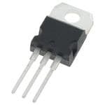
| 描述 | IC REG LDO 15V 0.5A TO220AB线性稳压器 15V 500mA Positive |
| 产品分类 | |
| 品牌 | ON Semiconductor |
| 产品手册 | |
| 产品图片 |
|
| rohs | 符合RoHS无铅 / 符合限制有害物质指令(RoHS)规范要求 |
| 产品系列 | 电源管理 IC,线性稳压器,ON Semiconductor MC78M15ACTG- |
| 数据手册 | |
| 产品型号 | MC78M15ACTG |
| PSRR/纹波抑制—典型值 | 70 dB |
| 产品种类 | |
| 供应商器件封装 | TO-220AB |
| 包装 | 管件 |
| 商标 | ON Semiconductor |
| 安装类型 | 通孔 |
| 安装风格 | Through Hole |
| 封装 | Tube |
| 封装/外壳 | TO-220-3 |
| 封装/箱体 | TO-220-3 |
| 工作温度 | 0°C ~ 125°C |
| 工厂包装数量 | 50 |
| 最大工作温度 | + 125 C |
| 最大输入电压 | 35 V |
| 最小工作温度 | 0 C |
| 最小输入电压 | 17 V |
| 极性 | Positive |
| 标准包装 | 50 |
| 电压-跌落(典型值) | 2V @ 350mA |
| 电压-输入 | 最高 35V |
| 电压-输出 | 15V |
| 电流-输出 | 500mA |
| 电流-限制(最小值) | - |
| 稳压器拓扑 | 正,固定式 |
| 稳压器数 | 1 |
| 系列 | MC78M15A |
| 线路调整率 | 50 mV |
| 负载调节 | 300 mV |
| 输出电压 | 15 V |
| 输出电流 | 0.5 A |
| 输出端数量 | 1 |
| 输出类型 | Fixed |


- 商务部:美国ITC正式对集成电路等产品启动337调查
- 曝三星4nm工艺存在良率问题 高通将骁龙8 Gen1或转产台积电
- 太阳诱电将投资9.5亿元在常州建新厂生产MLCC 预计2023年完工
- 英特尔发布欧洲新工厂建设计划 深化IDM 2.0 战略
- 台积电先进制程称霸业界 有大客户加持明年业绩稳了
- 达到5530亿美元!SIA预计今年全球半导体销售额将创下新高
- 英特尔拟将自动驾驶子公司Mobileye上市 估值或超500亿美元
- 三星加码芯片和SET,合并消费电子和移动部门,撤换高东真等 CEO
- 三星电子宣布重大人事变动 还合并消费电子和移动部门
- 海关总署:前11个月进口集成电路产品价值2.52万亿元 增长14.8%


PDF Datasheet 数据手册内容提取
MC78M00, MC78M00A, NCV78M00 Series 500 mA Positive Voltage Regulators The MC78M00/MC78M00A Series positive voltage regulators are identical to the popular MC7800 Series devices, except that they are www.onsemi.com specified for only half the output current. Like the MC7800 devices, the MC78M00 three−terminal regulators are intended for local, MARKING DIAGRAMS on−card voltage regulation. Internal current limiting, thermal shutdown circuitry and safe−area compensation for the internal pass transistor combine to make these TO−220 devices remarkably rugged under most operating conditions. T SUFFIX MC Maximum output current, with adequate heatsinking is 500 mA. CASE 221AB 78MxxXXT AWLYWWG Heatsink surface Features connected to Pin 2. • 1 No External Components Required 2 • 3 Internal Thermal Overload Protection xx = Voltage Option • Internal Short Circuit Current Limiting XX = Appropriate Suffix Options • Output Transistor Safe−Area Compensation A = Assembly Location • MC78M00A High Accuracy (±2%) WL = Wafer Lot Y = Year Available for 5.0 V, 8.0 V, 12 V and 15 V WW= Work Week • G = Pb−Free Package NCV Prefix for Automotive and Other Applications Requiring Unique Site and Control Change Requirements; AEC−Q100 4 Qualified and PPAP Capable DPAK−3 xxxxxG • These are Pb−Free Devices DT SUFFIX ALYWW 1 2 CASE 369C 3 Input 1.0 k 1.0 k 210 Heatsink surface (shown as terminal 4 in case outline drawing) is connected to Pin 2. 6.7 V 16 k xxxxx = Device Type and Voltage Option Code 100 A = Assembly Location 300 1.0 k 200 L = Wafer Lot Y = Year 3.6 k 3.0 k WW = Work Week 6.4 pF 300 G = Pb−Free Package k 5.6 k 10 0.24 Pin 1.Input 13 2.Ground 3.Output 20 50 200 Output 5 40 pF 6 k 6.0 k ORDERING INFORMATION 2. See detailed ordering and shipping information in the package 2.0 k 3.9 k dimensions section on page 10−14 of this data sheet. DEVICE MARKING INFORMATION 6.0 2.8 k k GND See general marking information in the device marking section on page 10 of this data sheet. This device contains 28 active transistors. Figure 1. Representative Schematic Diagram © Semiconductor Components Industries, LLC, 2016 1 Publication Order Number: March, 2016 − Rev. 28 MC78M00/D
MC78M00, MC78M00A, NCV78M00 Series MAXIMUM RATINGS (TA = 25°C, unless otherwise noted) (Note 1) Rating Symbol Value Unit Input Voltage VI Vdc (5.0 V−18 V) 35 (20 V−24V) 40 Power Dissipation (Package Limitation) °C/W Plastic Package, T Suffix TA = 25°C PD Internally Limited Thermal Resistance, Junction-to-Air (cid:2) 70 JA Thermal Resistance, Junction-to-Case (cid:2) 5.0 JC Plastic Package, DT Suffix TA = 25°C PD Internally Limited Thermal Resistance, Junction-to-Air (cid:2) 92 JA Thermal Resistance, Junction-to-Case (cid:2) 5.0 JC Operating Junction Temperature Range TJ +150 °C Storage Temperature Range Tstg −65 to +150 °C Stresses exceeding those listed in the Maximum Ratings table may damage the device. If any of these limits are exceeded, device functionality should not be assumed, damage may occur and reliability may be affected. 1. This device series contains ESD protection and exceeds the following tests: Human Body Model 2000 V per MIL−STD−883, Method 3015. Machine Model Method 200 V. MC78M05C/AC/B/AB, NCV78M05AB/B ELECTRICAL CHARACTERISTICS (VI = 10 V, IO = 350 mA, TJ = Tlow to Thigh, PD ≤ 5 W, unless otherwise noted) (Note 2) Characteristics Symbol Min Typ Max Unit Output Voltage (TJ = 25°C) VO Vdc MC78M05B/MC78M05C/NCV78M05B 4.8 5.0 5.2 MC78M05AB/MC78M05AC/NCV78M05AB 4.9 5.0 5.1 Output Voltage Variation (7.0 Vdc ≤ VI ≤ 20 Vdc, 5.0 mA ≤ IO ≤ 350 mA) VO Vdc MC78M05B/MC78M05C/NCV78M05B 4.75 − 5.25 MC78M05AB/MC78M05AC/NCV78M05AB 4.80 − 5.20 Line Regulation (TJ = 25°C, 7.0 Vdc ≤ VI ≤ 25 Vdc, IO = 200 mA) Regline − 3.0 50 mV Load Regulation Regload mV (TJ = 25°C, 5.0 mA ≤ IO ≤ 500 mA) − 20 100 (TJ = 25°C, 5.0 mA ≤ IO ≤ 200 mA) − 10 50 Input Bias Current (TJ = 25°C) IIB − 3.2 6.0 mA Quiescent Current Change (cid:3)IIB mA (8.0 Vdc ≤ VI ≤ 25 Vdc, IO = 200 mA) − − 0.8 (5.0 mA ≤ IO ≤ 350 mA) − − 0.5 Output Noise Voltage (TA = 25°C, 10 Hz ≤ f ≤ 100 kHz) Vn − 40 − (cid:4)V Ripple Rejection RR dB (IO = 100 mA, f = 120 Hz, 8.0 V ≤VI ≤ 18 V) 62 − − (IO = 300 mA, f = 120 Hz, 8.0 ≤ VI ≤ 18 V, TJ = 25°C) 62 80 − Dropout Voltage (TJ = 25°C) VI−VO − 2.0 − Vdc Short Circuit Current Limit (TJ = 25°C, VI = 35 V) IOS − 350 − mA Average Temperature Coefficient of Output Voltage (IO = 5.0 mA) (cid:3)VO/(cid:3)T − ±0.2 − mV/°C Peak Output Current (TJ = 25°C) IO − 700 − mA 2. Tlow= 0°C for MC78MxxAC, C = −40°C for MC78MxxAB, B, NCV78MxxAB, B Thigh = +125°C for MC78MxxAB, AC, B, C, NCV78MxxAB, B www.onsemi.com 2
MC78M00, MC78M00A, NCV78M00 Series MC78M06C/B ELECTRICAL CHARACTERISTICS (VI = 11 V, IO = 350 mA, TJ = Tlow to Thigh, PD ≤ 5.0 W, unless otherwise noted) (Note 3) Characteristics Symbol Min Typ Max Unit Output Voltage (TJ = 25°C) VO 5.75 6.0 6.25 Vdc Output Voltage Variation (8.0 Vdc ≤ VI ≤ 21 Vdc, 5.0 mA ≤ IO ≤ 350 mA) VO 5.7 − 6.3 Vdc Line Regulation (TJ = 25°C, 8.0 Vdc ≤ VI ≤ 25 Vdc, IO = 200 mA) Regline − 5.0 50 mV Load Regulation Regload mV (TJ = 25°C, 5.0 mA ≤ IO ≤ 500 Ma) − 20 120 (TJ = 25°C, 5.0 mA ≤ IO ≤ 200 mA) − 10 60 Input Bias Current (TJ = 25°C) IIB − 3.2 6.0 mA Quiescent Current Change (cid:3)IIB mA (9.0 Vdc ≤ VI ≤ 25 Vdc, IO = 200 mA) − − 0.8 (5.0 mA ≤ IO ≤ 350 mA) − − 0.5 Output Noise Voltage (TA = 25°C, 10 Hz ≤ f ≤ 100 kHz) Vn − 45 − (cid:4)V Ripple Rejection RR dB (IO = 100 mA, f = 120 Hz, 9.0 V ≤VI ≤ 19 V) 59 − − (IO = 300 mA, f = 120 Hz, 9.0 V ≤VI ≤ 19 V, TJ = 25°C) 59 80 − Dropout Voltage (TJ = 25°C) VI − VO − 2.0 − Vdc Short Circuit Current Limit (TJ = 25°C, VI = 35 V) IOS − 350 − mA Average Temperature Coefficient of Output Voltage (IO = 5.0 mA) (cid:3)VO/(cid:3)T − ±0.2 − mV/°C Peak Output Current (TJ = 25°C) IO − 700 − mA MC78M08C/AC/B/AB, NCV78M08B ELECTRICAL CHARACTERISTICS (VI = 14 V, IO = 350 mA, TJ = Tlow to Thigh, PD ≤ 5 W, unless otherwise noted) (Note 3) Characteristics Symbol Min Typ Max Unit Output Voltage (TJ = 25°C) VO Vdc MC78M08B/MC78M08C/NCV78M08B 7.70 8.0 8.30 MC78M08AB/MC78M08AC 7.84 8.0 8.16 Output Voltage Variation (10.5 Vdc ≤ VI ≤ 23 Vdc, 5.0 mA ≤ IO ≤ 350 mA) VO Vdc MC78M08B/MC78M08C/NCV78M08B 7.6 − 8.4 MC78M08AB/MC78M08AC 7.7 − 8.3 Line Regulation (TJ = 25°C, 10.5 Vdc ≤ VI ≤ 25 Vdc, IO = 200 mA) Regline − 6.0 50 mV Load Regulation Regload mV (TJ = 25°C, 5.0 mA ≤ IO ≤ 500 mA) − 25 160 (TJ = 25°C, 5.0 mA ≤ IO ≤ 200 mA) − 10 80 Input Bias Current (TJ = 25°C) IIB − 3.2 6.0 mA Quiescent Current Change (cid:3)IIB mA (10.5 Vdc ≤ VI ≤ 25 Vdc, IO = 200 mA) − − 0.8 (5.0 mA ≤ IO ≤ 350 mA) − − 0.5 Output Noise Voltage (TA = 25°C, 10 Hz ≤ f ≤ 100 kHz) Vn − 52 − (cid:4)V Ripple Rejection RR dB (IO = 100 mA, f = 120 Hz, 11.5 V ≤VI ≤ 21.5 V) 56 − − (IO = 300 mA, f = 120 Hz, 11.5 V ≤VI ≤ 21.5 V, TJ = 25°C) 56 80 − Dropout Voltage (TJ = 25°C) VI−VO − 2.0 − Vdc Short Circuit Current Limit (TJ = 25°C, VI = 35 V) IOS − 350 − mA Average Temperature Coefficient of Output Voltage (IO = 5.0 mA) (cid:3)VO/(cid:3)T − ±0.2 − mV/°C Peak Output Current (TJ = 25°C) IO − 700 − mA 3. Tlow= 0°C for MC78MxxAC, C = −40°C for MC78MxxAB, B, NCV78MxxAB, B Thigh = +125°C for MC78MxxAB, AC, B, C, NCV78MxxAB, B www.onsemi.com 3
MC78M00, MC78M00A, NCV78M00 Series MC78M09C/B, NCV78M09B ELECTRICAL CHARACTERISTICS (VI = 15 V, IO = 350 mA, TJ = Tlow to Thigh, PD ≤ 5.0 W, unless otherwise noted) (Note 4) Characteristics Symbol Min Typ Max Unit Output Voltage (TJ = 25°C) VO 8.64 9.0 9.45 Vdc Output Voltage Variation (11.5 Vdc ≤ VI ≤ 23 Vdc, 5.0 mA ≤ IO ≤ 350 mA) VO 8.55 − 9.45 Vdc Line Regulation (TJ = 25°C, 11.5 Vdc ≤ VI ≤ 25 Vdc, IO = 200 mA) Regline − 6.0 50 mV Load Regulation Regload mV (TJ = 25°C, 5.0 mA ≤ IO ≤ 500 mA) − 25 180 (TJ = 25°C, 5.0 mA ≤ IO ≤ 200 mA) − 10 90 Input Bias Current (TJ = 25°C) IIB − 3.2 6.0 mA Quiescent Current Change (cid:3)IIB mA (11.5 Vdc ≤ VI ≤ 25 Vdc, IO = 200 mA) − − 0.8 (5.0 mA ≤ IO ≤ 350 mA) − − 0.5 Output Noise Voltage (TA = 25°C, 10 Hz ≤ f ≤ 100 kHz) Vn − 52 − (cid:4)V Ripple Rejection RR dB (IO = 100 mA, f = 120 Hz, 12.5 V ≤VI ≤ 22.5 V) 56 − − (IO = 300 mA, f = 120 Hz, 12.5 V ≤VI ≤ 22.5 V, TJ = 25°C) 56 80 − Dropout Voltage (TJ = 25°C) VI−VO − 2.0 − Vdc Short Circuit Current Limit (TJ = 25°C, VI = 35 V) IOS − 350 − mA Average Temperature Coefficient of Output Voltage (IO = 5.0 mA) (cid:3)VO/(cid:3)T − ±0.2 − mV/°C Peak Output Current (TJ = 25°C) IO − 700 − mA MC78M12C/AC/B/AB, NCV78M12B ELECTRICAL CHARACTERISTICS (VI = 19 V, IO = 350 mA, TJ = Tlow to Thigh, PD ≤ 5 W, unless otherwise noted) (Note 4) Characteristics Symbol Min Typ Max Unit Output Voltage (TJ = 25°C) VO Vdc MC78M12B/MC78M12C/NCV78M12B 11.50 12 12.50 MC78M12AB/MC78M12AC 11.76 12 12.24 Output Voltage Variation (14.5 Vdc ≤ VI ≤ 27 Vdc, 5.0 mA ≤ IO ≤ 350 mA) VO Vdc MC78M12B/MC78M12C/NCV78M12B 11.4 − 12.6 MC78M12AB/MC78M12AC 11.5 − 12.5 Line Regulation (TJ = 25°C, 14.5 Vdc ≤ VI ≤ 30 Vdc, IO = 200 mA) Regline − 8.0 50 mV Load Regulation Regload mV (TJ = 25°C, 5.0 mA ≤ IO ≤ 500 mA) − 25 240 (TJ = 25°C, 5.0 mA ≤ IO ≤ 200 mA) − 10 120 Input Bias Current (TJ = 25°C) IIB − 3.2 6.0 mA Quiescent Current Change (cid:3)IIB mA (14.5 Vdc ≤ VI ≤ 30 Vdc, IO = 200 mA) − − 0.8 (5.0 mA ≤ IO ≤ 350 mA) − − 0.5 Output Noise Voltage (TA = 25°C, 10 Hz ≤ f ≤ 100 kHz) Vn − 75 − (cid:4)V Ripple Rejection RR dB (IO = 100 mA, f = 120 Hz, 15 V ≤VI ≤ 25 V) 55 − − (IO = 300 mA, f = 120 Hz, 15 V ≤VI ≤ 25 V, TJ = 25°C) 55 80 − Dropout Voltage (TJ = 25°C) VI−VO − 2.0 − Vdc Short Circuit Current Limit (TJ = 25°C, VI = 35 V) IOS − 350 − mA Average Temperature Coefficient of Output Voltage (IO = 5.0 mA) (cid:3)VO/(cid:3)T − ±0.3 − mV/°C Peak Output Current (TJ = 25°C) IO − 700 − mA 4. Tlow= 0°C for MC78MxxAC, C = −40°C for MC78MxxAB, B, NCV78MxxAB, B Thigh = +125°C for MC78MxxAB, AC, B, C, NCV78MxxAB, B www.onsemi.com 4
MC78M00, MC78M00A, NCV78M00 Series MC78M15C/AC/B/AB, NCV78M15B ELECTRICAL CHARACTERISTICS (VI = 23 V, IO = 350 mA, TJ = Tlow to Thigh, PD ≤ 5 W, unless otherwise noted) (Note 5) Characteristics Symbol Min Typ Max Unit Output Voltage (TJ = 25°C) VO Vdc MC78M15B/MC78M15C/NCV78M15B 14.4 15 15.6 MC78M15AB/MC78M15AC 14.7 15 15.3 Output Voltage Variation (17.5 Vdc ≤ VI ≤ 30 Vdc, 5.0 mA ≤ IO ≤ 350 mA) VO Vdc MC78M15B/MC78M15C/NCV78M15B 14.25 − 15.75 MC78M15AB/MC78M15AC 14.40 − 15.60 Input Regulation (TJ = 25°C, 17.5 Vdc ≤ VI ≤ 30 Vdc, IO = 200 mA) Regline − 10 50 mV Load Regulation Regload mV (TJ = 25°C, 5.0 mA ≤ IO ≤ 500 mA) − 25 300 (TJ = 25°C, 5.0 mA ≤ IO ≤ 200 mA) − 10 150 Input Bias Current (TJ = 25°C) IIB − 3.2 6.0 mA Quiescent Current Change (cid:3)IIB mA (17.5 Vdc ≤ VI ≤ 30 Vdc, IO = 200 mA) − − 0.8 (5.0 mA ≤ IO ≤ 350 mA) − − 0.5 Output Noise Voltage (TA = 25°C, 10 Hz ≤ f ≤ 100 kHz) Vn − 90 − (cid:4)V Ripple Rejection RR dB (IO = 100 mA, f = 120 Hz, 18.5 V ≤VI ≤ 28.5 V) 54 − − (IO = 300 mA, f = 120 Hz, 18.5 V ≤VI ≤ 28.5 V, TJ = 25°C) 54 70 − Dropout Voltage (TJ = 25°C) VI−VO − 2.0 − Vdc Short Circuit Current Limit (TJ = 25°C, VI = 35 V) IOS − 350 − mA Average Temperature Coefficient of Output Voltage (IO = 5.0 mA) (cid:3)VO/(cid:3)T − ±0.3 − mV/°C Peak Output Current (TJ = 25°C) IO − 700 − mA MC78M18C/B ELECTRICAL CHARACTERISTICS (VI = 27 V, IO = 350 mA, TJ = Tlow to Thigh, PD ≤ 5 W, unless otherwise noted) (Note 5) Characteristics Symbol Min Typ Max Unit Output Voltage (TJ = 25°C) VO 17.3 18 18.7 Vdc Output Voltage Variation (21 Vdc ≤ VI ≤ 33 Vdc, 5.0 mA ≤ IO ≤ 350 mA) VO 17.1 − 18.9 Vdc Line Regulation (TJ = 25°C, 21 Vdc ≤ VI ≤ 33 Vdc, IO = 200 mA) Regline − 10 50 mV Load Regulation Regload mV (TJ = 25°C, 5.0 mA ≤ IO ≤ 500 mA) − 30 360 (TJ = 25°C, 5.0 mA ≤ IO ≤ 200 mA) − 10 180 Input Bias Current (TJ = 25°C) IIB − 3.2 6.5 mA Quiescent Current Change (cid:3)IIB mA (21 Vdc ≤ VI ≤ 33 Vdc, IO = 200 mA) − − 0.8 (5.0 mA ≤ IO ≤ 350 mA) − − 0.5 Output Noise Voltage (TA = 25°C, 10 Hz ≤ f ≤ 100 kHz) Vn − 100 − (cid:4)V Ripple Rejection RR dB (IO = 100 mA, f = 120 Hz, 22 V ≤VI ≤ 32 V) 53 − − (IO = 300 mA, f = 120 Hz, 22 V ≤VI ≤ 32 V, TJ = 25°C) 53 70 − Dropout Voltage (TJ = 25°C) VI−VO − 2.0 − Vdc Short Circuit Current Limit (TJ = 25°C, VI = 35 V) IOS − 350 − mA Average Temperature Coefficient of Output Voltage (IO = 5.0 mA) (cid:3)VO/(cid:3)T − ±0.3 − mV/°C Peak Output Current (TJ = 25°C) IO − 700 − mA 5. Tlow= 0°C for MC78MxxAC, C = −40°C for MC78MxxAB, B, NCV78MxxAB, B Thigh = +125°C for MC78MxxAB, AC, B, C, NCV78MxxAB, B www.onsemi.com 5
MC78M00, MC78M00A, NCV78M00 Series MC78M20C/B ELECTRICAL CHARACTERISTICS (VI = 29 V, IO = 350 mA, TJ = Tlow to Thigh, PD ≤ 5.0 W, unless otherwise noted) (Note 6) Characteristics Symbol Min Typ Max Unit Output Voltage (TJ = 25°C) VO 19.2 20 20.8 Vdc Output Voltage Variation (23 Vdc ≤ VI ≤ 35 Vdc, 5.0 mA ≤ IO ≤ 350 mA) VO 19 − 21 Vdc Line Regulation (TJ = 25°C, 23 Vdc ≤ VI ≤ 35 Vdc, IO = 200 mA) Regline − 10 50 mV Load Regulation Regload mV (TJ = 25°C, 5.0 mA ≤ IO ≤ 500 mA) − 30 400 (TJ = 25°C, 5.0 mA ≤ IO ≤ 200 mA) − 10 200 Input Bias Current (TJ = 25°C) IIB − 3.2 6.5 mA Quiescent Current Change (cid:3)IIB mA (23 Vdc ≤ VI ≤ 35 Vdc, IO = 200 mA) − − 0.8 (5.0 mA ≤ IO ≤ 350 mA) − − 0.5 Output Noise Voltage (TA = 25°C, 10 Hz ≤ f ≤ 100 kHz) Vn − 110 − (cid:4)V Ripple Rejection RR dB (IO = 100 mA, f = 120 Hz, 24 V ≤VI ≤ 34 V) 52 − − (IO = 300 mA, f = 120 Hz, 24 V ≤VI ≤ 34 V, TJ = 25°C) 52 70 − Dropout Voltage (TJ = 25°C) VI−VO − 2.0 − Vdc Short Circuit Current Limit (TJ = 25°C, VI = 35 V) IOS − 350 − mA Average Temperature Coefficient of Output Voltage (IO = 5.0 mA) (cid:3)VO/(cid:3)T − ±0.5 − mV/°C Peak Output Current (TJ = 25°C) IO − 700 − mA MC78M24C/B ELECTRICAL CHARACTERISTICS (VI = 33 V, IO = 350 mA, TJ = Tlow to Thigh, PD ≤ 5.0 W, unless otherwise noted) (Note 6) Characteristics Symbol Min Typ Max Unit Output Voltage (TJ = 25°C) VO 23 24 25 Vdc Output Voltage Variation (27 Vdc ≤ VI ≤ 38 Vdc, 5.0 mA ≤ IO ≤ 350 mA) VO 22.8 − 25.2 Vdc Line Regulation (TJ = 25°C, 27 Vdc ≤ VI ≤ 38 Vdc, IO = 200 mA) Regline − 10 50 mV Load Regulation Regload mV (TJ = 25°C, 5.0 mA ≤ IO ≤ 500 mA) − 30 480 (TJ = 25°C, 5.0 mA ≤ IO ≤ 200 mA) − 10 240 Input Bias Current (TJ = 25°C) IIB − 3.2 7.0 mA Quiescent Current Change (cid:3)IIB mA (27 Vdc ≤ VI ≤ 38 Vdc, IO = 200 mA) − − 0.8 (5.0 mA ≤ IO ≤ 350 mA) − − 0.5 Output Noise Voltage (TA = 25°C, 10 Hz ≤ f ≤ 100 kHz) Vn − 170 − (cid:4)V Ripple Rejection RR dB (IO = 100 mA, f = 120 Hz, 28 V ≤VI ≤ 38 V) 50 − − (IO = 300 mA, f = 120 Hz, 28 V ≤VI ≤ 38 V, TJ = 25°C) 50 70 − Dropout Voltage (TJ = 25°C) VI−VO − 2.0 − Vdc Short Circuit Current Limit (TJ = 25°C) IOS − 350 − mA Average Temperature Coefficient of Output Voltage (IO = 5.0 mA) (cid:3)VO/(cid:3)T − ±0.5 − mV/°C Peak Output Current (TJ = 25°C) IO − 700 − mA 6. Tlow= 0°C for MC78MxxAC, C = −40°C for MC78MxxAB, B Thigh = +125°C for MC78MxxAB, AC, B, C www.onsemi.com 6
MC78M00, MC78M00A, NCV78M00 Series DEFINITIONS Line Regulation − The change in output voltage for a Input Bias Current − That part of the input current that change in the input voltage. The measurement is made under is not delivered to the load. conditions of low dissipation or by using pulse techniques Output Noise Voltage − The rms AC voltage at the such that the average chip temperature is not significantly output, with constant load and no input ripple, measured affected. over a specified frequency range. Load Regulation − The change in output voltage for a Long Term Stability − Output voltage stability under change in load current at constant chip temperature. accelerated life test conditions with the maximum rated Maximum Power Dissipation − The maximum total voltage listed in the devices’ electrical characteristics and device dissipation for which the regulator will operate maximum power dissipation. within specifications. 100 Free Air PD(max) for TA = 50°C 2.4 N (W) NCE W) 90 VMeoruticnatelldy 2.0 PATIO RESISTA°AIR ( C/ 80 Minimum Î2.0 oÎz. CLoÎpperÎ1.6 ER DISSI , THERMAL θJAJUNCTION-TO- 567000 Size Pad ÎÎL ÎÎÎÎÎÎ001...482 MAXIMUM POW R R(cid:2)JA P, D 40 0 0 5.0 10 15 20 25 30 L, LENGTH OF COPPER (mm) Figure 2. DPAK Thermal Resistance and Maximum Power Dissipation versus P.C.B. Copper Length 10 Infinite Heat (cid:2)HS = 10°C/W Sink W) 5.0 ON ( 3.0 (cid:2)HS = 20°C/W ATI 2.0 SIP No Heat Sink S DI 1.0 R E W 0.5 O P , D 0.3 P 0.2 (cid:2)JC = 5°C/W PD(max) = 7.52 W 0.1 25 50 75 100 125 150 TA, AMBIENT TEMPERATURE (°C) Figure 3. Worst Case Power Dissipation versus Ambient Temperature (TO−220) www.onsemi.com 7
MC78M00, MC78M00A, NCV78M00 Series 1.0 2.5 0.9 V) ENT (A) 00..87 TJ = 25°C OLTAGE ( 2.0 IO = 500 mA , OUTPUT CURRIO 00000.....65432 TJ = 125°C , DROPOUT V-VO110...505 (cid:3)VO = 100 mV IIOO == 11000 m mAA 0.1 VI 0 0 0 5.0 10 15 20 25 30 35 40 0 25 50 75 100 125 150 VI - VO, DROPOUT VOLTAGE (V) TJ, JUNCTION TEMPERATURE (°C) Figure 4. Peak Output Current versus Figure 5. Dropout Voltage versus Dropout Voltage Junction Temperature 100 100 Iout = 500 mA B) B) d d N ( 80 N ( 80 O O TI TI C C E E EJ 60 Iout = 500 mA EJ RR, RIPPLE R 40 VVCTJoiOn u = t== = 2 10 550°. 0CV V RR, RIPPLE R 60 VVCfT =JoiOn u = 1t== 2= 2 100 550 °H. 0CVz V 40 20 30 1.0 10 100 1.0 k 10 k 100 k 1.0 M 10 M 100 M 0.01 0.1 0.5 1.0 10 f, FREQUENCY (Hz) IO, OUTPUT CURRENT (A) Figure 6. Ripple Rejection versus Frequency Figure 7. Ripple Rejection versus Output Current 4.0 5.0 TJ = 25°C A) 3.0 A) 4.0 TJ = 25°C m m T ( T ( EN EN 3.0 URR 2.0 TJ = 125°C URR C C S S 2.0 , BIAIB 1.0 TJT =J 1=2 255°°CC VIOO = = 0 5.5.0 A V , BIAIB 1.0 TJ = 125°C VI-VO = 5.0 V 0 0 0 5.0 10 15 20 25 30 35 40 0.01 0.1 0.5 1.0 10 VI, INPUT VOLTAGE (Vdc) IO, OUTPUT CURRENT (A) Figure 8. Bias Current versus Input Voltage Figure 9. Bias Current versus Output Current www.onsemi.com 8
MC78M00, MC78M00A, NCV78M00 Series APPLICATIONS INFORMATION Design Considerations regulator is connected to the power supply filter with long wire lengths, or if the output load capacitance is large. An The MC78M00/MC78M00A Series of fixed voltage input bypass capacitor should be selected to provide good regulators are designed with Thermal Overload Protection high frequency characteristics to insure stable operation that shuts down the circuit when subjected to an excessive under all load conditions. A 0.33 (cid:4)F or larger tantalum, power overload condition, Internal Short Circuit Protection mylar, or other capacitor having low internal impedance at that limits the maximum current the circuit will pass, and high frequencies should be chosen. The bypass capacitor Output Transistor Safe−Area Compensation that reduces the should be mounted with the shortest possible leads directly output short circuit current as the voltage across the pass across the regulator’s input terminals. Normally good transistor is increased. construction techniques should be used to minimize ground In many low current applications, compensation loops and lead resistance drops since the regulator has no capacitors are not required. However, it is recommended external sense lead. that the regulator input be bypassed with a capacitor if the Input MC78M05C VViOn-, V7.o0u tV ≥ t o2 .200 V V 0.33 (cid:4)F R Constant Output Current to MC78M05C Grounded Input IO Load 7 2 (cid:2) The MC78M00 regulators can also be used as a current source 0.33 (cid:4)F 6 0.1 (cid:4)F when connected as above. In order to minimize dissipation the MC78M05C is chosen in this application. Resistor R determines 3 + 10 k the current as follows: 1.0 k 4 MC1741 5.0 V IO = R + IIB IIB = 1.5 mA over line and load changes. The addition of an operational amplifier allows adjustment to higher For example, a 500 mA current source would require R to be a or intermediate values while retaining regulation characteristics. 10(cid:2)(cid:5), 10 W resistor and the output voltage compliance would be The minimum voltage obtainable with this arrangement is 2.0 V the input voltage less 7.0 V. greater than the regulator voltage. Figure 10. Current Regulator Figure 11. Adjustable Output Regulator MJ2955 or Equiv. MJ2955 or Equiv. Input RSC Input R MC78MXXC Output 2N6049 or Equiv. R MC78MXXC 1.0 (cid:4)F 1.0 (cid:4)F Output 1.0 (cid:4)F XX = 2 digits of type number indicating voltage. XX = 2 digits of type number indicating voltage. The MC78M00 series can be current boosted with a PNP The circuit of Figure 12 can be modified to provide supply protection transistor. The MJ2955 provides current to 5.0 A. Resistor R in against short circuits by adding a short circuit sense resistor, Rsc, conjunction with the VBE of the PNP determines when the pass and an additional PNP transistor. The current sensing PNP must be transistor begins conducting; this circuit is not short circuit able to handle the short circuit current of the three-terminal proof. Input-output differential voltage minimum is increased regulator .Therefore, a 4.0 A plastic power transistor is specified. by VBE of the pass transistor. Figure 12. Current Boost Regulator Figure 13. Current Boost with Short Circuit Protection www.onsemi.com 9
MC78M00, MC78M00A, NCV78M00 Series ORDERING INFORMATION Output Device Voltage Temperature Range Package Marking Shipping† MC78M05CDTG 5.0 V TJ = 0° to +125°C DPAK−3 78M05 75 Units / Rail (Pb−Free) MC78M05CDTT5G 5.0 V TJ = 0° to +125°C DPAK−3 78M05 2500 / Tape & Reel (Pb−Free) MC78M05CDTRKG 5.0 V TJ = 0° to +125°C DPAK−3 78M05 2500 / Tape & Reel (Pb−Free) MC78M05ACDTG 5.0 V TJ = 0° to +125°C DPAK−3 8M05D 75 Units / Rail (Pb−Free) MC78M05ACDTRKG 5.0 V TJ = 0° to +125°C DPAK−3 8M05D 2500 / Tape & Reel (Pb−Free) MC78M05CTG 5.0 V TJ = 0° to +125°C TO−220 78M05CT 50 Units / Rail (Pb−Free) MC78M05ACTG 5.0 V TJ = 0° to +125°C TO−220 78M05ACT 50 Units / Rail (Pb−Free) MC78M05ABDTG 5.0 V TJ = −40° to +125°C DPAK−3 8M05A 75 Units / Rail (Pb−Free) MC78M05ABDTRKG 5.0 V TJ = −40° to +125°C DPAK−3 8M05A 2500 / Tape & Reel (Pb−Free) NCV78M05ABDTRKG* 5.0 V TJ = −40° to +125°C DPAK−3 8M05A 2500 / Tape & Reel (Pb−Free) MC78M05ABTG 5.0 V TJ = −40° to +125°C TO−220 78M05ABT 50 Units / Rail (Pb−Free) MC78M05BDTG 5.0 V TJ = −40° to +125°C DPAK−3 8M05B 75 Units / Rail (Pb−Free) MC78M05BDTT5G 5.0 V TJ = −40° to +125°C DPAK−3 8M05B 2500 / Tape & Reel (Pb−Free) MC78M05BDTRKG 5.0 V TJ = −40° to +125°C DPAK−3 8M05B 2500 / Tape & Reel (Pb−Free) NCV78M05BDTRKG* 5.0 V TJ = −40° to +125°C DPAK−3 8M05B 2500 / Tape & Reel (Pb−Free) MC78M05BTG 5.0 V TJ = −40° to +125°C TO−220 78M05BT 50 Units / Rail (Pb−Free) NCV78M05BTG* 5.0 V TJ = −40° to +125°C TO−220 78M05BT 50 Units / Rail (Pb−Free) MC78M06CDTG 6.0 V TJ = 0° to +125°C DPAK−3 78M06 75 Units / Rail (Pb−Free) MC78M06CDTRKG 6.0 V TJ = 0° to +125°C DPAK−3 78M06 2500 / Tape & Reel (Pb−Free) MC78M06CTG 6.0 V TJ = 0° to +125°C TO−220 78M06CT 50 Units / Rail (Pb−Free) MC78M06BTG 6.0 V TJ = −40° to +125°C TO−220 78M06BT 50 Units / Rail (Pb−Free) MC78M06BDTRKG 6.0 V TJ = −40° to +125°C DPAK−3 8M06B 2500 / Tape & Reel (Pb−Free) MC78M08CDTG 8.0 V TJ = 0° to +125°C DPAK−3 78M08 75 Units / Rail (Pb−Free) †For information on tape and reel specifications, including part orientation and tape sizes, please refer to our Tape and Reel Packaging Specifications Brochure, BRD8011/D. *NCV devices: Tlow = −40°C, Thigh = +125°C. Guaranteed by design. NCV Prefix for Automotive and Other Applications Requiring Unique Site and Control Change Requirements; AEC−Q100 Qualified and PPAP Capable. www.onsemi.com 10
MC78M00, MC78M00A, NCV78M00 Series ORDERING INFORMATION (continued) OOuuttppuutt DDeevviiccee VVoollttaaggee TTeemmppeerraattuurree RRaannggee PPaacckkaaggee MMaarrkkiinngg SShhiippppiinngg†† MC78M08CDTRKG 8.0 V TJ = 0° to +125°C DPAK−3 78M08 2500 Units / Tape & Reel (Pb−Free) MC78M08ACDTG 8.0 V TJ = 0° to +125°C DPAK−3 8M08D 75 Units / Rail (Pb−Free) MC78M08ACDTRKG 8.0 V TJ = 0° to +125°C DPAK−3 8M08D 2500 Units / Tape & Reel (Pb−Free) MC78M08CTG 8.0 V TJ = 0° to +125°C TO−220 78M08CT 50 Units / Rail (Pb−Free) MC78M08ACTG 8.0 V TJ = 0° to +125°C TO−220 78M08ACT 50 Units / Rail (Pb−Free) MC78M08ABDTG 8.0 V TJ = −40° to +125°C DPAK−3 8M08A 75 Units / Rail (Pb−Free) MC78M08ABDTRKG 8.0 V TJ = −40° to +125°C DPAK−3 8M08A 2500 Units / Tape & Reel (Pb−Free) MC78M08ABTG 8.0 V TJ = −40° to +125°C TO−220 78M08ABT 50 Units / Rail (Pb−Free) MC78M08BDTG 8.0 V TJ = −40° to +125°C DPAK−3 8M08B 75 Units / Rail (Pb−Free) MC78M08BDTRKG 8.0 V TJ = −40° to +125°C DPAK−3 8M08B 2500 Units / Tape & Reel (Pb−Free) NCV78M08BDTRKG* 8.0 V TJ = −40° to +125°C DPAK−3 8M08B 2500 Units / Tape & Reel (Pb−Free) MC78M08BTG 8.0 V TJ = −40° to +125°C TO−220 78M08BT 50 Units / Rail (Pb−Free) MC78M09CDTG 9.0 V TJ = 0° to +125°C DPAK−3 78M09 75 Units / Rail (Pb−Free) MC78M09CDTRKG 9.0 V TJ = 0° to +125°C DPAK−3 78M09 2500 Units / Tape & Reel (Pb−Free) MC78M09CTG 9.0 V TJ = 0° to +125°C TO−220 78M09CT 50 Units / Rail (Pb−Free) MC78M09BDTG 9.0 V TJ = −40° to +125°C DPAK−3 8M09B 75 Units / Rail (Pb−Free) MC78M09BDTRKG 9.0 V TJ = −40° to +125°C DPAK−3 8M09B 2500 Units / Tape & Reel (Pb−Free) NCV78M09BDTRKG* 9.0 V TJ = −40° to +125°C DPAK−3 8M09B 2500 Units / Tape & Reel (Pb−Free) MC78M12CDTG 12 V TJ = 0° to +125°C DPAK−3 78M12 75 Units / Rail (Pb−Free) MC78M12CDTT5G 12 V TJ = 0° to +125°C DPAK−3 78M12 2500 Units / Tape & Reel (Pb−Free) MC78M12CDTRKG 12 V TJ = 0° to +125°C DPAK−3 78M12 2500 Units / Tape & Reel (Pb−Free) MC78M12ACDTG 12 V TJ = 0° to +125°C DPAK−3 8M12D 75 Units / Rail (Pb−Free) MC78M12ACDTRKG 12 V TJ = 0° to +125°C DPAK−3 8M12D 2500 Units / Tape & Reel (Pb−Free) †For information on tape and reel specifications, including part orientation and tape sizes, please refer to our Tape and Reel Packaging Specifications Brochure, BRD8011/D. *NCV devices: Tlow = −40°C, Thigh = +125°C. Guaranteed by design. NCV Prefix for Automotive and Other Applications Requiring Unique Site and Control Change Requirements; AEC−Q100 Qualified and PPAP Capable. www.onsemi.com 11
MC78M00, MC78M00A, NCV78M00 Series ORDERING INFORMATION (continued) OOuuttppuutt DDeevviiccee VVoollttaaggee TTeemmppeerraattuurree RRaannggee PPaacckkaaggee MMaarrkkiinngg SShhiippppiinngg†† MC78M12CTG 12 V TJ = 0° to +125°C TO−220 78M12CT 50 Units / Rail (Pb−Free) MC78M12ACTG 12 V TJ = 0° to +125°C TO−220 78M12ACT 50 Units / Rail (Pb−Free) MC78M12ABDTG 12 V TJ = −40° to +125°C DPAK−3 8M12A 75 Units / Rail (Pb−Free) MC78M12ABDTRKG 12 V TJ = −40° to +125°C DPAK−3 8M12A 2500 Units / Tape & Reel (Pb−Free) MC78M12ABTG 12 V TJ = −40° to +125°C TO−220 78M12ABT 50 Units / Rail (Pb−Free) MC78M12BDTG 12 V TJ = −40° to +125°C DPAK−3 8M12B 75 Units / Rail (Pb−Free) MC78M12BDTRKG 12 V TJ = −40° to +125°C DPAK−3 8M12B 2500 Units / Tape & Reel (Pb−Free) NCV78M12BDTRKG* 12 V TJ = −40° to +125°C DPAK−3 8M12B 2500 Units / Tape & Reel (Pb−Free) MC78M12BTG 12 V TJ = −40° to +125°C TO−220 78M12BT 50 Units / Rail (Pb−Free) MC78M15CDTG 15 V TJ = 0° to +125°C DPAK−3 78M15 75 Units / Rail (Pb−Free) MC78M15CDTT5G 15 V TJ = 0° to +125°C DPAK−3 78M15 2500 Units / Tape & Reel (Pb−Free) MC78M15CDTRKG 15 V TJ = 0° to +125°C DPAK−3 78M15 2500 Units / Tape & Reel (Pb−Free) MC78M15ACDTG 15 V TJ = 0° to +125°C DPAK−3 8M15D 75 Units / Rail (Pb−Free) MC78M15ACDTRKG 15 V TJ = 0° to +125°C DPAK−3 8M15D 2500 Units / Tape & Reel (Pb−Free) MC78M15CTG 15 V TJ = 0° to +125°C TO−220 78M15CT 50 Units / Rail (Pb−Free) MC78M15ACTG 15 V TJ = 0° to +125°C TO−220 78M15ACT 50 Units / Rail (Pb−Free) MC78M15ABDTG 15 V TJ = −40° to +125°C DPAK−3 8M15A 75 Units / Rail (Pb−Free) MC78M15ABDTRKG 15 V TJ = −40° to +125°C DPAK−3 8M15A 2500 Units / Tape & Reel (Pb−Free) MC78M15ABTG 15 V TJ = −40° to +125°C TO−220 78M15ABT 50 Units / Rail (Pb−Free) MC78M15BDTG 15 V TJ = −40° to +125°C DPAK−3 8M15B 75 Units / Rail (Pb−Free) NCV78M15BDTG* 15 V TJ = −40° to +125°C DPAK−3 8M15B 75 Units / Rail (Pb−Free) MC78M15BDTRKG 15 V TJ = −40° to +125°C DPAK−3 8M15B 2500 Units / Tape & Reel (Pb−Free) NCV78M15BDTRKG* 15 V TJ = −40° to +125°C DPAK−3 8M15B 2500 Units / Tape & Reel (Pb−Free) †For information on tape and reel specifications, including part orientation and tape sizes, please refer to our Tape and Reel Packaging Specifications Brochure, BRD8011/D. *NCV devices: Tlow = −40°C, Thigh = +125°C. Guaranteed by design. NCV Prefix for Automotive and Other Applications Requiring Unique Site and Control Change Requirements; AEC−Q100 Qualified and PPAP Capable. www.onsemi.com 12
MC78M00, MC78M00A, NCV78M00 Series ORDERING INFORMATION (continued) OOuuttppuutt DDeevviiccee VVoollttaaggee TTeemmppeerraattuurree RRaannggee PPaacckkaaggee MMaarrkkiinngg SShhiippppiinngg†† MC78M15BTG 15 V TJ = −40° to +125°C TO−220 78M15BT 50 Units / Rail (Pb−Free) MC78M18CDTG 18 V TJ = 0° to +125°C DPAK−3 78M18 75 Units / Rail (Pb−Free) MC78M18CDTRKG 18 V TJ = 0° to +125°C DPAK−3 78M18 2500 Units / Tape & Reel (Pb−Free) MC78M18CTG 18 V TJ = 0° to +125°C TO−220 78M18CT 50 Units / Rail (Pb−Free) MC78M18BTG 18 V TJ = −40° to +125°C TO−220 78M18BT 50 Units / Rail (Pb−Free) MC78M20CTG 20 V TJ = 0° to +125°C TO−220 78M20CT 50 Units / Rail (Pb−Free) MC78M24CTG 24 V TJ = 0° to +125°C TO−220 78M24CT 50 Units / Rail (Pb−Free) MC78M24BTG 24 V TJ = −40° to +125°C TO−220 78M24BT 50 Units / Rail (Pb−Free) †For information on tape and reel specifications, including part orientation and tape sizes, please refer to our Tape and Reel Packaging Specifications Brochure, BRD8011/D. *NCV devices: Tlow = −40°C, Thigh = +125°C. Guaranteed by design. NCV Prefix for Automotive and Other Applications Requiring Unique Site and Control Change Requirements; AEC−Q100 Qualified and PPAP Capable. www.onsemi.com 13
MC78M00, MC78M00A, NCV78M00 Series PACKAGE DIMENSIONS DPAK−3 DT SUFFIX CASE 369C ISSUE F NOTES: A 1.DIMENSIONING AND TOLERANCING PER ASME Y14.5M, 1994. E C 2.CONTROLLING DIMENSION: INCHES. A 3.THERMAL PAD CONTOUR OPTIONAL WITHIN DI- b3 B MENSIONS b3, L3 and Z. c2 4.DIMENSIONS D AND E DO NOT INCLUDE MOLD FLASH, PROTRUSIONS, OR BURRS. MOLD FLASH, PROTRUSIONS, OR GATE BURRS SHALL 4 NOT EXCEED 0.006 INCHES PER SIDE. L3 Z 5.DIMENSIONS D AND E ARE DETERMINED AT THE D DETAIL A H 6.DOAUTTUEMRSM OA SATN EDX BT RAERME EDSE OTEFR TMHIEN EPDLA ASTT DICA TBUOMDY. 1 2 3 PLANE H. 7.OPTIONAL MOLD FEATURE. L4 INCHES MILLIMETERS NOTE 7 b2 c BOTTOM VIEW DIM MIN MAX MIN MAX A 0.086 0.094 2.18 2.38 e SIDE VIEW A1 0.000 0.005 0.00 0.13 b b 0.025 0.035 0.63 0.89 0.005 (0.13) M C b2 0.028 0.045 0.72 1.14 TOP VIEW b3 0.180 0.215 4.57 5.46 c 0.018 0.024 0.46 0.61 c2 0.018 0.024 0.46 0.61 H Z Z D 0.235 0.245 5.97 6.22 E 0.250 0.265 6.35 6.73 e 0.090 BSC 2.29 BSC L2 GPLAAUNGEE C SPELAATNIENG HL 00..035750 00..047100 19..4400 101..4718 L1 0.114 REF 2.90 REF L2 0.020 BSC 0.51 BSC L A1 BOTTOM VIEW L3 0.035 0.050 0.89 1.27 L1 ALTERNATE L4 −−− 0.040 −−− 1.01 CONSTRUCTIONS Z 0.155 −−− 3.93 −−− DETAIL A ROTATED 90(cid:2) CW SOLDERING FOOTPRINT* 6.20 3.00 0.244 0.118 2.58 0.102 5.80 1.60 6.17 0.228 0.063 0.243 (cid:3) (cid:4) mm SCALE 3:1 inches *For additional information on our Pb−Free strategy and soldering details, please download the ON Semiconductor Soldering and Mounting Techniques Reference Manual, SOLDERRM/D. www.onsemi.com 14
MC78M00, MC78M00A, NCV78M00 Series PACKAGE DIMENSIONS TO−220, SINGLE GAUGE CASE 221AB ISSUE A NOTES: 1. DIMENSIONING AND TOLERANCING PER ANSI Y14.5M, 1982. −T− SPELAATNIENG 23.. CDOIMNETNRSOIOLLNI NZG D DEFIMINEENSS IAO ZNO: INNEC WHEHSE.RE ALL BODY AND B F C LEAD IRREGULARITIES ARE ALLOWED. 4. PRODUCT SHIPPED PRIOR TO 2008 HAD DIMENSIONS T S S = 0.045 - 0.055 INCHES (1.143 - 1.397 MM) 4 INCHES MILLIMETERS DIM MIN MAX MIN MAX Q A A 0.570 0.620 14.48 15.75 B 0.380 0.405 9.66 10.28 C 0.160 0.190 4.07 4.82 1 2 3 U D 0.025 0.035 0.64 0.88 H F 0.142 0.147 3.61 3.73 G 0.095 0.105 2.42 2.66 K H 0.110 0.155 2.80 3.93 Z J 0.018 0.025 0.46 0.64 K 0.500 0.562 12.70 14.27 L 0.045 0.060 1.15 1.52 N 0.190 0.210 4.83 5.33 L R Q 0.100 0.120 2.54 3.04 V J R 0.080 0.110 2.04 2.79 S 0.020 0.024 0.508 0.61 G T 0.235 0.255 5.97 6.47 U 0.000 0.050 0.00 1.27 D V 0.045 --- 1.15 --- N Z --- 0.080 --- 2.04 ON Semiconductor and the are registered trademarks of Semiconductor Components Industries, LLC (SCILLC) or its subsidiaries in the United States and/or other countries. SCILLC owns the rights to a number of patents, trademarks, copyrights, trade secrets, and other intellectual property. A listing of SCILLC’s product/patent coverage may be accessed at www.onsemi.com/site/pdf/Patent−Marking.pdf. SCILLC reserves the right to make changes without further notice to any products herein. SCILLC makes no warranty, representation or guarantee regarding the suitability of its products for any particular purpose, nor does SCILLC assume any liability arising out of the application or use of any product or circuit, and specifically disclaims any and all liability, including without limitation special, consequential or incidental damages. “Typical” parameters which may be provided in SCILLC data sheets and/or specifications can and do vary in different applications and actual performance may vary over time. All operating parameters, including “Typicals” must be validated for each customer application by customer’s technical experts. SCILLC does not convey any license under its patent rights nor the rights of others. SCILLC products are not designed, intended, or authorized for use as components in systems intended for surgical implant into the body, or other applications intended to support or sustain life, or for any other application in which the failure of the SCILLC product could create a situation where personal injury or death may occur. Should Buyer purchase or use SCILLC products for any such unintended or unauthorized application, Buyer shall indemnify and hold SCILLC and its officers, employees, subsidiaries, affiliates, and distributors harmless against all claims, costs, damages, and expenses, and reasonable attorney fees arising out of, directly or indirectly, any claim of personal injury or death associated with such unintended or unauthorized use, even if such claim alleges that SCILLC was negligent regarding the design or manufacture of the part. SCILLC is an Equal Opportunity/Affirmative Action Employer. This literature is subject to all applicable copyright laws and is not for resale in any manner. PUBLICATION ORDERING INFORMATION LITERATURE FULFILLMENT: N. American Technical Support: 800−282−9855 Toll Free ON Semiconductor Website: www.onsemi.com Literature Distribution Center for ON Semiconductor USA/Canada 19521 E. 32nd Pkwy, Aurora, Colorado 80011 USA Europe, Middle East and Africa Technical Support: Order Literature: http://www.onsemi.com/orderlit Phone: 303−675−2175 or 800−344−3860 Toll Free USA/Canada Phone: 421 33 790 2910 Fax: 303−675−2176 or 800−344−3867 Toll Free USA/Canada Japan Customer Focus Center For additional information, please contact your local Email: orderlit@onsemi.com Phone: 81−3−5817−1050 Sales Representative www.onsemi.com MC78M00/D 15